EP3312900B1 - Display device - Google Patents
Display device Download PDFInfo
- Publication number
- EP3312900B1 EP3312900B1 EP17192152.1A EP17192152A EP3312900B1 EP 3312900 B1 EP3312900 B1 EP 3312900B1 EP 17192152 A EP17192152 A EP 17192152A EP 3312900 B1 EP3312900 B1 EP 3312900B1
- Authority
- EP
- European Patent Office
- Prior art keywords
- adhesive layer
- optical film
- layer
- display device
- phase retarder
- Prior art date
- Legal status (The legal status is an assumption and is not a legal conclusion. Google has not performed a legal analysis and makes no representation as to the accuracy of the status listed.)
- Active
Links
Images




Classifications
-
- B—PERFORMING OPERATIONS; TRANSPORTING
- B32—LAYERED PRODUCTS
- B32B—LAYERED PRODUCTS, i.e. PRODUCTS BUILT-UP OF STRATA OF FLAT OR NON-FLAT, e.g. CELLULAR OR HONEYCOMB, FORM
- B32B27/00—Layered products comprising a layer of synthetic resin
- B32B27/28—Layered products comprising a layer of synthetic resin comprising synthetic resins not wholly covered by any one of the sub-groups B32B27/30 - B32B27/42
- B32B27/281—Layered products comprising a layer of synthetic resin comprising synthetic resins not wholly covered by any one of the sub-groups B32B27/30 - B32B27/42 comprising polyimides
-
- B—PERFORMING OPERATIONS; TRANSPORTING
- B32—LAYERED PRODUCTS
- B32B—LAYERED PRODUCTS, i.e. PRODUCTS BUILT-UP OF STRATA OF FLAT OR NON-FLAT, e.g. CELLULAR OR HONEYCOMB, FORM
- B32B15/00—Layered products comprising a layer of metal
- B32B15/04—Layered products comprising a layer of metal comprising metal as the main or only constituent of a layer, which is next to another layer of the same or of a different material
- B32B15/08—Layered products comprising a layer of metal comprising metal as the main or only constituent of a layer, which is next to another layer of the same or of a different material of synthetic resin
-
- B—PERFORMING OPERATIONS; TRANSPORTING
- B32—LAYERED PRODUCTS
- B32B—LAYERED PRODUCTS, i.e. PRODUCTS BUILT-UP OF STRATA OF FLAT OR NON-FLAT, e.g. CELLULAR OR HONEYCOMB, FORM
- B32B15/00—Layered products comprising a layer of metal
- B32B15/20—Layered products comprising a layer of metal comprising aluminium or copper
-
- B—PERFORMING OPERATIONS; TRANSPORTING
- B32—LAYERED PRODUCTS
- B32B—LAYERED PRODUCTS, i.e. PRODUCTS BUILT-UP OF STRATA OF FLAT OR NON-FLAT, e.g. CELLULAR OR HONEYCOMB, FORM
- B32B23/00—Layered products comprising a layer of cellulosic plastic substances, i.e. substances obtained by chemical modification of cellulose, e.g. cellulose ethers, cellulose esters, viscose
-
- B—PERFORMING OPERATIONS; TRANSPORTING
- B32—LAYERED PRODUCTS
- B32B—LAYERED PRODUCTS, i.e. PRODUCTS BUILT-UP OF STRATA OF FLAT OR NON-FLAT, e.g. CELLULAR OR HONEYCOMB, FORM
- B32B23/00—Layered products comprising a layer of cellulosic plastic substances, i.e. substances obtained by chemical modification of cellulose, e.g. cellulose ethers, cellulose esters, viscose
- B32B23/04—Layered products comprising a layer of cellulosic plastic substances, i.e. substances obtained by chemical modification of cellulose, e.g. cellulose ethers, cellulose esters, viscose comprising such cellulosic plastic substance as the main or only constituent of a layer, which is next to another layer of the same or of a different material
-
- B—PERFORMING OPERATIONS; TRANSPORTING
- B32—LAYERED PRODUCTS
- B32B—LAYERED PRODUCTS, i.e. PRODUCTS BUILT-UP OF STRATA OF FLAT OR NON-FLAT, e.g. CELLULAR OR HONEYCOMB, FORM
- B32B27/00—Layered products comprising a layer of synthetic resin
- B32B27/06—Layered products comprising a layer of synthetic resin as the main or only constituent of a layer, which is next to another layer of the same or of a different material
-
- B—PERFORMING OPERATIONS; TRANSPORTING
- B32—LAYERED PRODUCTS
- B32B—LAYERED PRODUCTS, i.e. PRODUCTS BUILT-UP OF STRATA OF FLAT OR NON-FLAT, e.g. CELLULAR OR HONEYCOMB, FORM
- B32B27/00—Layered products comprising a layer of synthetic resin
- B32B27/28—Layered products comprising a layer of synthetic resin comprising synthetic resins not wholly covered by any one of the sub-groups B32B27/30 - B32B27/42
- B32B27/286—Layered products comprising a layer of synthetic resin comprising synthetic resins not wholly covered by any one of the sub-groups B32B27/30 - B32B27/42 comprising polysulphones; polysulfides
-
- B—PERFORMING OPERATIONS; TRANSPORTING
- B32—LAYERED PRODUCTS
- B32B—LAYERED PRODUCTS, i.e. PRODUCTS BUILT-UP OF STRATA OF FLAT OR NON-FLAT, e.g. CELLULAR OR HONEYCOMB, FORM
- B32B27/00—Layered products comprising a layer of synthetic resin
- B32B27/30—Layered products comprising a layer of synthetic resin comprising vinyl (co)polymers; comprising acrylic (co)polymers
- B32B27/308—Layered products comprising a layer of synthetic resin comprising vinyl (co)polymers; comprising acrylic (co)polymers comprising acrylic (co)polymers
-
- B—PERFORMING OPERATIONS; TRANSPORTING
- B32—LAYERED PRODUCTS
- B32B—LAYERED PRODUCTS, i.e. PRODUCTS BUILT-UP OF STRATA OF FLAT OR NON-FLAT, e.g. CELLULAR OR HONEYCOMB, FORM
- B32B27/00—Layered products comprising a layer of synthetic resin
- B32B27/36—Layered products comprising a layer of synthetic resin comprising polyesters
-
- B—PERFORMING OPERATIONS; TRANSPORTING
- B32—LAYERED PRODUCTS
- B32B—LAYERED PRODUCTS, i.e. PRODUCTS BUILT-UP OF STRATA OF FLAT OR NON-FLAT, e.g. CELLULAR OR HONEYCOMB, FORM
- B32B27/00—Layered products comprising a layer of synthetic resin
- B32B27/36—Layered products comprising a layer of synthetic resin comprising polyesters
- B32B27/365—Layered products comprising a layer of synthetic resin comprising polyesters comprising polycarbonates
-
- B—PERFORMING OPERATIONS; TRANSPORTING
- B32—LAYERED PRODUCTS
- B32B—LAYERED PRODUCTS, i.e. PRODUCTS BUILT-UP OF STRATA OF FLAT OR NON-FLAT, e.g. CELLULAR OR HONEYCOMB, FORM
- B32B3/00—Layered products comprising a layer with external or internal discontinuities or unevennesses, or a layer of non-planar shape; Layered products comprising a layer having particular features of form
- B32B3/26—Layered products comprising a layer with external or internal discontinuities or unevennesses, or a layer of non-planar shape; Layered products comprising a layer having particular features of form characterised by a particular shape of the outline of the cross-section of a continuous layer; characterised by a layer with cavities or internal voids ; characterised by an apertured layer
- B32B3/28—Layered products comprising a layer with external or internal discontinuities or unevennesses, or a layer of non-planar shape; Layered products comprising a layer having particular features of form characterised by a particular shape of the outline of the cross-section of a continuous layer; characterised by a layer with cavities or internal voids ; characterised by an apertured layer characterised by a layer comprising a deformed thin sheet, i.e. the layer having its entire thickness deformed out of the plane, e.g. corrugated, crumpled
-
- B—PERFORMING OPERATIONS; TRANSPORTING
- B32—LAYERED PRODUCTS
- B32B—LAYERED PRODUCTS, i.e. PRODUCTS BUILT-UP OF STRATA OF FLAT OR NON-FLAT, e.g. CELLULAR OR HONEYCOMB, FORM
- B32B7/00—Layered products characterised by the relation between layers; Layered products characterised by the relative orientation of features between layers, or by the relative values of a measurable parameter between layers, i.e. products comprising layers having different physical, chemical or physicochemical properties; Layered products characterised by the interconnection of layers
- B32B7/02—Physical, chemical or physicochemical properties
-
- B—PERFORMING OPERATIONS; TRANSPORTING
- B32—LAYERED PRODUCTS
- B32B—LAYERED PRODUCTS, i.e. PRODUCTS BUILT-UP OF STRATA OF FLAT OR NON-FLAT, e.g. CELLULAR OR HONEYCOMB, FORM
- B32B7/00—Layered products characterised by the relation between layers; Layered products characterised by the relative orientation of features between layers, or by the relative values of a measurable parameter between layers, i.e. products comprising layers having different physical, chemical or physicochemical properties; Layered products characterised by the interconnection of layers
- B32B7/04—Interconnection of layers
- B32B7/12—Interconnection of layers using interposed adhesives or interposed materials with bonding properties
-
- H—ELECTRICITY
- H10—SEMICONDUCTOR DEVICES; ELECTRIC SOLID-STATE DEVICES NOT OTHERWISE PROVIDED FOR
- H10K—ORGANIC ELECTRIC SOLID-STATE DEVICES
- H10K50/00—Organic light-emitting devices
- H10K50/80—Constructional details
- H10K50/84—Passivation; Containers; Encapsulations
- H10K50/842—Containers
- H10K50/8426—Peripheral sealing arrangements, e.g. adhesives, sealants
-
- H—ELECTRICITY
- H10—SEMICONDUCTOR DEVICES; ELECTRIC SOLID-STATE DEVICES NOT OTHERWISE PROVIDED FOR
- H10K—ORGANIC ELECTRIC SOLID-STATE DEVICES
- H10K50/00—Organic light-emitting devices
- H10K50/80—Constructional details
- H10K50/84—Passivation; Containers; Encapsulations
- H10K50/844—Encapsulations
-
- H—ELECTRICITY
- H10—SEMICONDUCTOR DEVICES; ELECTRIC SOLID-STATE DEVICES NOT OTHERWISE PROVIDED FOR
- H10K—ORGANIC ELECTRIC SOLID-STATE DEVICES
- H10K50/00—Organic light-emitting devices
- H10K50/80—Constructional details
- H10K50/84—Passivation; Containers; Encapsulations
- H10K50/844—Encapsulations
- H10K50/8445—Encapsulations multilayered coatings having a repetitive structure, e.g. having multiple organic-inorganic bilayers
-
- H—ELECTRICITY
- H10—SEMICONDUCTOR DEVICES; ELECTRIC SOLID-STATE DEVICES NOT OTHERWISE PROVIDED FOR
- H10K—ORGANIC ELECTRIC SOLID-STATE DEVICES
- H10K50/00—Organic light-emitting devices
- H10K50/80—Constructional details
- H10K50/86—Arrangements for improving contrast, e.g. preventing reflection of ambient light
-
- H—ELECTRICITY
- H10—SEMICONDUCTOR DEVICES; ELECTRIC SOLID-STATE DEVICES NOT OTHERWISE PROVIDED FOR
- H10K—ORGANIC ELECTRIC SOLID-STATE DEVICES
- H10K59/00—Integrated devices, or assemblies of multiple devices, comprising at least one organic light-emitting element covered by group H10K50/00
- H10K59/30—Devices specially adapted for multicolour light emission
- H10K59/38—Devices specially adapted for multicolour light emission comprising colour filters or colour changing media [CCM]
-
- H—ELECTRICITY
- H10—SEMICONDUCTOR DEVICES; ELECTRIC SOLID-STATE DEVICES NOT OTHERWISE PROVIDED FOR
- H10K—ORGANIC ELECTRIC SOLID-STATE DEVICES
- H10K59/00—Integrated devices, or assemblies of multiple devices, comprising at least one organic light-emitting element covered by group H10K50/00
- H10K59/80—Constructional details
- H10K59/8791—Arrangements for improving contrast, e.g. preventing reflection of ambient light
-
- H—ELECTRICITY
- H10—SEMICONDUCTOR DEVICES; ELECTRIC SOLID-STATE DEVICES NOT OTHERWISE PROVIDED FOR
- H10K—ORGANIC ELECTRIC SOLID-STATE DEVICES
- H10K77/00—Constructional details of devices covered by this subclass and not covered by groups H10K10/80, H10K30/80, H10K50/80 or H10K59/80
- H10K77/10—Substrates, e.g. flexible substrates
- H10K77/111—Flexible substrates
-
- B—PERFORMING OPERATIONS; TRANSPORTING
- B32—LAYERED PRODUCTS
- B32B—LAYERED PRODUCTS, i.e. PRODUCTS BUILT-UP OF STRATA OF FLAT OR NON-FLAT, e.g. CELLULAR OR HONEYCOMB, FORM
- B32B2255/00—Coating on the layer surface
- B32B2255/06—Coating on the layer surface on metal layer
-
- B—PERFORMING OPERATIONS; TRANSPORTING
- B32—LAYERED PRODUCTS
- B32B—LAYERED PRODUCTS, i.e. PRODUCTS BUILT-UP OF STRATA OF FLAT OR NON-FLAT, e.g. CELLULAR OR HONEYCOMB, FORM
- B32B2255/00—Coating on the layer surface
- B32B2255/26—Polymeric coating
-
- B—PERFORMING OPERATIONS; TRANSPORTING
- B32—LAYERED PRODUCTS
- B32B—LAYERED PRODUCTS, i.e. PRODUCTS BUILT-UP OF STRATA OF FLAT OR NON-FLAT, e.g. CELLULAR OR HONEYCOMB, FORM
- B32B2255/00—Coating on the layer surface
- B32B2255/28—Multiple coating on one surface
-
- B—PERFORMING OPERATIONS; TRANSPORTING
- B32—LAYERED PRODUCTS
- B32B—LAYERED PRODUCTS, i.e. PRODUCTS BUILT-UP OF STRATA OF FLAT OR NON-FLAT, e.g. CELLULAR OR HONEYCOMB, FORM
- B32B2307/00—Properties of the layers or laminate
- B32B2307/40—Properties of the layers or laminate having particular optical properties
- B32B2307/402—Coloured
-
- B—PERFORMING OPERATIONS; TRANSPORTING
- B32—LAYERED PRODUCTS
- B32B—LAYERED PRODUCTS, i.e. PRODUCTS BUILT-UP OF STRATA OF FLAT OR NON-FLAT, e.g. CELLULAR OR HONEYCOMB, FORM
- B32B2307/00—Properties of the layers or laminate
- B32B2307/40—Properties of the layers or laminate having particular optical properties
- B32B2307/416—Reflective
-
- B—PERFORMING OPERATIONS; TRANSPORTING
- B32—LAYERED PRODUCTS
- B32B—LAYERED PRODUCTS, i.e. PRODUCTS BUILT-UP OF STRATA OF FLAT OR NON-FLAT, e.g. CELLULAR OR HONEYCOMB, FORM
- B32B2457/00—Electrical equipment
- B32B2457/20—Displays, e.g. liquid crystal displays, plasma displays
- B32B2457/206—Organic displays, e.g. OLED
-
- G—PHYSICS
- G02—OPTICS
- G02B—OPTICAL ELEMENTS, SYSTEMS OR APPARATUS
- G02B5/00—Optical elements other than lenses
- G02B5/30—Polarising elements
- G02B5/3025—Polarisers, i.e. arrangements capable of producing a definite output polarisation state from an unpolarised input state
- G02B5/3033—Polarisers, i.e. arrangements capable of producing a definite output polarisation state from an unpolarised input state in the form of a thin sheet or foil, e.g. Polaroid
- G02B5/3041—Polarisers, i.e. arrangements capable of producing a definite output polarisation state from an unpolarised input state in the form of a thin sheet or foil, e.g. Polaroid comprising multiple thin layers, e.g. multilayer stacks
-
- G—PHYSICS
- G09—EDUCATION; CRYPTOGRAPHY; DISPLAY; ADVERTISING; SEALS
- G09F—DISPLAYING; ADVERTISING; SIGNS; LABELS OR NAME-PLATES; SEALS
- G09F9/00—Indicating arrangements for variable information in which the information is built-up on a support by selection or combination of individual elements
- G09F9/30—Indicating arrangements for variable information in which the information is built-up on a support by selection or combination of individual elements in which the desired character or characters are formed by combining individual elements
- G09F9/301—Indicating arrangements for variable information in which the information is built-up on a support by selection or combination of individual elements in which the desired character or characters are formed by combining individual elements flexible foldable or roll-able electronic displays, e.g. thin LCD, OLED
-
- H—ELECTRICITY
- H10—SEMICONDUCTOR DEVICES; ELECTRIC SOLID-STATE DEVICES NOT OTHERWISE PROVIDED FOR
- H10K—ORGANIC ELECTRIC SOLID-STATE DEVICES
- H10K2102/00—Constructional details relating to the organic devices covered by this subclass
- H10K2102/301—Details of OLEDs
- H10K2102/311—Flexible OLED
-
- H—ELECTRICITY
- H10—SEMICONDUCTOR DEVICES; ELECTRIC SOLID-STATE DEVICES NOT OTHERWISE PROVIDED FOR
- H10K—ORGANIC ELECTRIC SOLID-STATE DEVICES
- H10K50/00—Organic light-emitting devices
- H10K50/80—Constructional details
- H10K50/868—Arrangements for polarized light emission
-
- H—ELECTRICITY
- H10—SEMICONDUCTOR DEVICES; ELECTRIC SOLID-STATE DEVICES NOT OTHERWISE PROVIDED FOR
- H10K—ORGANIC ELECTRIC SOLID-STATE DEVICES
- H10K59/00—Integrated devices, or assemblies of multiple devices, comprising at least one organic light-emitting element covered by group H10K50/00
- H10K59/10—OLED displays
- H10K59/12—Active-matrix OLED [AMOLED] displays
-
- H—ELECTRICITY
- H10—SEMICONDUCTOR DEVICES; ELECTRIC SOLID-STATE DEVICES NOT OTHERWISE PROVIDED FOR
- H10K—ORGANIC ELECTRIC SOLID-STATE DEVICES
- H10K59/00—Integrated devices, or assemblies of multiple devices, comprising at least one organic light-emitting element covered by group H10K50/00
- H10K59/80—Constructional details
- H10K59/87—Passivation; Containers; Encapsulations
- H10K59/871—Self-supporting sealing arrangements
-
- H—ELECTRICITY
- H10—SEMICONDUCTOR DEVICES; ELECTRIC SOLID-STATE DEVICES NOT OTHERWISE PROVIDED FOR
- H10K—ORGANIC ELECTRIC SOLID-STATE DEVICES
- H10K59/00—Integrated devices, or assemblies of multiple devices, comprising at least one organic light-emitting element covered by group H10K50/00
- H10K59/80—Constructional details
- H10K59/87—Passivation; Containers; Encapsulations
- H10K59/871—Self-supporting sealing arrangements
- H10K59/8722—Peripheral sealing arrangements, e.g. adhesives, sealants
-
- H—ELECTRICITY
- H10—SEMICONDUCTOR DEVICES; ELECTRIC SOLID-STATE DEVICES NOT OTHERWISE PROVIDED FOR
- H10K—ORGANIC ELECTRIC SOLID-STATE DEVICES
- H10K59/00—Integrated devices, or assemblies of multiple devices, comprising at least one organic light-emitting element covered by group H10K50/00
- H10K59/80—Constructional details
- H10K59/87—Passivation; Containers; Encapsulations
- H10K59/873—Encapsulations
- H10K59/8731—Encapsulations multilayered coatings having a repetitive structure, e.g. having multiple organic-inorganic bilayers
-
- Y—GENERAL TAGGING OF NEW TECHNOLOGICAL DEVELOPMENTS; GENERAL TAGGING OF CROSS-SECTIONAL TECHNOLOGIES SPANNING OVER SEVERAL SECTIONS OF THE IPC; TECHNICAL SUBJECTS COVERED BY FORMER USPC CROSS-REFERENCE ART COLLECTIONS [XRACs] AND DIGESTS
- Y02—TECHNOLOGIES OR APPLICATIONS FOR MITIGATION OR ADAPTATION AGAINST CLIMATE CHANGE
- Y02E—REDUCTION OF GREENHOUSE GAS [GHG] EMISSIONS, RELATED TO ENERGY GENERATION, TRANSMISSION OR DISTRIBUTION
- Y02E10/00—Energy generation through renewable energy sources
- Y02E10/50—Photovoltaic [PV] energy
- Y02E10/549—Organic PV cells
Definitions
- aspects of one or more embodiments relate to a display device.
- a display device includes a display unit over a substrate and displaying an image. At least a portion of the display device may be bent or folded, and thus the display device may be viewed at various angles and portability of the display device may be improved by reducing the volume of the display device.
- the display device may include an optical film which may prevent external light reflection.
- the optical film may improve visibility and contrast of an image by preventing light incident to the display device from being reflected by a metallic layer, etc. of the display device and being viewed by a user.
- An optical film of a bendable or foldable display device of the related art, preventing external light reflection may receive tensile force or compressive force occurring while the display device is bent or folded.
- tensile force or compressive force occurring while the display device is bent or folded.
- layers between layers of the optical film and/or adjacent to the optical film are floated, and moisture penetrates into the optical film via the floated region, and thus a polarizer of the optical film is denaturalized. That is, at least a portion of the optical film may not prevent external light reflection and thus quality of an image produced by the display device may deteriorate.
- US 2016/0293895 A1 discloses a display device including a display panel, a polarizer on the display panel, an adhesion layer on the polarizer, and a window on the adhesion layer, the window including a light transmissive window base, a light shielding layer on the window base and a protrusion on the light shielding layer.
- US 2011/0007391 A1 concerns a display apparatus with protection plate and a manufacturing method thereof.
- US 2012/0012828 A1 concerns an organic light-emitting device including a substrate, an encapsulation substrate, an organic light-emitting unit interposed between the substrate and the encapsulation substrate, and a layer having an UV shielding capability interposed between the encapsulation substrate and the organic light-emitting unit.
- a display device has improved quality of a produced image by preventing or reducing penetration of moisture into an optical film.
- this aspect is provided as an example and the scope of the disclosure is not limited thereto.
- a display device comprises the features of claim 1.
- a display device includes: a display panel to display an image; an optical film over the display panel and including at least one phase retarder and a polarizer; a first adhesive layer between the display panel and the optical film and contacting a first surface of the optical film; and a second adhesive layer on the optical film and contacting a second surface of the optical film opposite the first surface, wherein the first adhesive layer and the second adhesive layer contact each other.
- the at least one phase retarder comprises a 1/4 wavelength phase retarder, and a pressure sensitive adhesive or an adhesive is between the 1/4 wavelength phase retarder and the polarizer, wherein the at least one phase retarder further comprises a 1/2 wavelength phase retarder adjacent to the 1/4 wavelength phase and over the display panel, and the pressure sensitive adhesive or the adhesive is between the 1/4 wavelength phase retarder and the 1/2 wavelength phase retarder and between the 1/2 wavelength phase retarder and the polarizer, wherein the 1/4 wavelength phase retarder includes a reactive liquid crystal, wherein the reactive liquid crystal is a discotic liquid crystal or a nematic liquid crystal.
- At least one of the first adhesive layer and the second adhesive layer includes a respective protrusion region protruding toward an outside of the optical film.
- the protrusion region may surround a perimeter of the optical film.
- the display panel may include a bending area bent around a bending axis extending in a direction, at least a portion of the optical film being in the bending area.
- the protrusion region may include a first protrusion region and a second protrusion region spaced apart from each other in the direction in which the bending axis extends.
- the first adhesive layer and the second adhesive layer may include a same material.
- the display panel may include a display area and a non-display area, the display panel having an area greater than that of the optical film, and the optical film completely covering the display area.
- the display device may further include: a window over the optical film; and a colored layer along an edge region of an inner surface of the window.
- At least one of the first adhesive layer and the second adhesive layer may cover at least a portion of the colored layer.
- the protrusion region of the at least one of the first adhesive layer and the second adhesive layer may have a thickness about three times to about fifty times greater than a thickness of the colored layer.
- the second adhesive layer may include the protrusion region, the protrusion region covering an end of the optical film and an end of the first adhesive layer.
- the first adhesive layer may have a same area as that of the optical film.
- the first adhesive layer may include the protrusion region, the protrusion region covering an end of the optical film and an end of the second adhesive layer.
- the second adhesive layer may have a same area as that of the optical film.
- Each of the first adhesive layer and the second adhesive layer may include the protrusion region, the protrusion region of the first adhesive layer contacting the protrusion region of the second adhesive layer at an outer edge of the optical film.
- the display panel may include: a flexible substrate; and an organic light-emitting device over the flexible substrate and including a pixel electrode, an intermediate layer, and an opposite electrode, the intermediate layer including an organic emission layer.
- the display panel may further include: a protective film below the flexible substrate; and an encapsulation layer over the flexible substrate, covering the organic light-emitting device, and including at least one inorganic encapsulation layer and at least one organic encapsulation layer.
- a display device includes: a display panel to display an image; an optical film over the display panel and including at least one phase retarder and a polarizer; a first adhesive layer between the display panel and the optical film and contacting a first surface of the optical film; and a second adhesive layer on the optical film and contacting a second surface of the optical film opposite the first surface, wherein at least one of the first adhesive layer and the second adhesive layer includes a protrusion region protruding toward an outside of the optical film, and the protrusion region covers an end of the optical film.
- the display device includes: a display panel according to claim 1 to display an image and including a bending area bent around a bending axis extending in a direction; and wherein at least a portion of the protrusion region is over the bending area of the display panel.
- a display device prevents or reduces quality deterioration of a produced image due to moisture penetrating into an optical film and at least a portion of the optical film losing an external light reflection prevention function.
- the scope of the disclosure is not limited to this effect.
- An embodiment of an inventive display combines the features of any of FIGs. 1 , 6 , 7 or 9 with the ones of FIG. 5 .
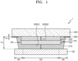
- a display device 1 includes a display panel 100 displaying an image, an optical film 200 over the display panel 100 and including at least one phase retarder 210 and a polarizer 220, a first adhesive layer 310 between the display panel 100 and the optical film 200 and contacting a first surface 200S1 of the optical film 200, and a second adhesive layer 320 on the optical film 200 and contacting a second surface 200S2 of the optical film 200, the first adhesive layer 310 contacting the second adhesive layer 320.
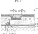
- the display panel 100 may include a substrate 120 and an organic light-emitting device (OLED) 130 over the substrate 120.
- the substrate 120 may be a flexible substrate.
- the substrate 120 may include a polymer resin, such as polyethersulfone (PES), polyacrylate (PAR), polyetherimide (PEI), polyethylene naphthalate (PEN), polyethylene terephthalate (PET), polyphenylene sulfide (PPS), polyallylate, polyimide (PI), polycarbonate (PC), or cellulose acetate propionate (CAP).
- PES polyethersulfone
- PAR polyacrylate
- PEI polyetherimide
- PEN polyethylene naphthalate
- PET polyethylene terephthalate
- PPS polyphenylene sulfide
- PI polyimide
- PC polycarbonate
- CAP cellulose acetate propionate
- a thin film transistor (TFT) electrically connected to the OLED 130 may be over the substrate 120.
- the TFT may include a semiconductor layer 122 including amorphous silicon, polycrystalline silicon, or an organic semiconductor material, a gate electrode 124, a source electrode 126S, and a drain electrode 126D.
- a gate insulating layer 123 may be between the semiconductor layer 122 and the gate electrode 124, the gate insulating layer 123 including an inorganic material, such as silicon oxide, silicon nitride, and/or silicon oxynitride.
- An interlayer insulating layer 125 may be on the gate electrode 124, the interlayer insulating layer 125 including an inorganic material, such as silicon oxide, silicon nitride, and/or silicon oxynitride.
- the source electrode 126S and the drain electrode 126D may be on the interlayer insulating layer 125.
- the insulating layers including an inorganic material may be formed by chemical vapor deposition (CVD) or atomic layer deposition (ALD).
- a buffer layer 121 may be between the substrate 120 and the TFT having the above structure, the buffer layer 121 including an inorganic material, such as silicon oxide, silicon nitride, and/or silicon oxynitride.
- the buffer layer 121 may increase planarization of the upper surface of the substrate 120, or prevent or minimize penetration of impurities from the substrate 120 into the semiconductor layer 122 of the TFT.
- a planarization layer 127 may be on the TFT.
- the planarization layer 127 may substantially planarize the TFT.
- the planarization layer 127 may include an organic material, such as PI, benzocyclobutene (BCB), or hexamethyldisiloxane (HMDSO).
- PI PI
- benzocyclobutene BCB
- HMDSO hexamethyldisiloxane
- the planarization layer 127 is shown as a single layer in FIG. 3 , the planarization layer 127 may be a multi-layer and variously selected.
- the OLED 130 may be on the planarization layer 127, the OLED 130 including a pixel electrode 131, an opposite electrode 135, and an intermediate layer 133 between the pixel electrode 131 and the opposite electrode 135, the intermediate layer 133 including an emission layer.
- the pixel electrode 131 is electrically connected to the TFT by contacting one of the source electrode 126S and the drain electrode 126D via an opening of the planarization layer 127.
- the pixel electrode 131 may be a reflective electrode including a reflective layer.
- the reflective layer may include at least one of Ag, Mg, Al, Pt, Pd, Au, Ni, Nd, Ir, and Cr.
- a transparent or semi-transparent electrode layer may be further over the reflective layer, the transparent or semi-transparent electrode layer including at least one of indium tin oxide (ITO), indium zinc oxide (IZO), zinc oxide (ZnO), indium oxide (In 2 O 3 ), indium gallium oxide (IGO), and aluminum zinc oxide (AZO).
- ITO indium tin oxide
- IZO indium zinc oxide
- ZnO zinc oxide
- IGO indium gallium oxide
- AZO aluminum zinc oxide
- the pixel electrode 131 may include three layers including ITO/Ag/ITO.
- a pixel-defining layer 129 may be on the planarization layer 127.
- the pixel-defining layer 129 defines a pixel by including an opening corresponding to each subpixel, that is, an opening exposing at least a central portion of the pixel electrode 131.
- the pixel-defining layer 129 may prevent an arc, etc. from occurring at an edge of the pixel electrode 131 by increasing a distance between the edge of the pixel electrode 131 and the opposite electrode 135 over the pixel electrode 131.
- the pixel-defining layer 129 may include an organic material, such as PI or HMDSO.
- the intermediate layer 133 of the OLED 130 may include an organic emission layer.
- the intermediate layer 133 may further include at least one of a hole injection layer (HIL), a hole transport layer (HTL), an electron transport layer (ETL), and an electron injection layer (EIL).
- HIL hole injection layer
- HTL hole transport layer
- ETL electron transport layer
- EIL electron injection layer
- the embodiment is not limited thereto and the intermediate layer 133 may further include any of various functional layers.
- the intermediate layer 133 is not limited to the above described layers and may have any of various structures. Also, the intermediate layer 133 may include a layer which is one body over a plurality of pixel electrodes 131 or include a layer patterned to respectively correspond to the pixel electrodes 131.
- the organic emission layer may have a multi-layered structure in which a red emission layer, a green emission layer, and a blue emission layer are stacked, or may have a single-layered structure including a red emission material, a green emission material, and a blue emission material.
- the OLED 130 including the organic emission layer may emit full colors by additionally including a red color filter, a green color filter, and a blue color filter.
- the opposite electrode 135 may be a (semi)-transparent electrode.
- the opposite electrode 135 may include at least one of Ag, Al, Mg, Li, Ca, Cu, LiF/Ca, MgAg, and CaAg.
- the opposite electrode 135 may include a thin layer which may transmit light, the thin layer having a thickness in a range from about several nm to about tens of nm.
- an encapsulation layer 140 may cover and protect the OLED.
- the encapsulation layer 140 may include a first inorganic encapsulation layer 141, an organic encapsulation layer 142, and a second inorganic encapsulation layer 143.
- the first inorganic encapsulation layer 141 may cover the opposite electrode 135 and include silicon oxide, silicon nitride, and/or silicon oxynitride. When needed, one or more other layers, such as a capping layer or a LiF layer, may be between the first inorganic encapsulation layer 141 and the opposite electrode 135. Since the first inorganic encapsulation layer 141 is along a structure therebeneath, the upper surface of the first inorganic encapsulation layer 141 is not planarized, as illustrated in FIG. 3 .
- the organic encapsulation layer 142 may cover the first inorganic encapsulation layer 141.
- the upper surface of the organic encapsulation layer 142 may be planarized.
- the organic encapsulation layer 142 may include at least one of PET, PEN, PC, PI, polyethylene sulfonate, polyoxymethylene, polyallylate, and HMDSO.
- the second inorganic encapsulation layer 143 may cover the organic encapsulation layer 142 and include silicon oxide, silicon nitride, and/or silicon oxynitride. The second inorganic encapsulation layer 143 may prevent the organic encapsulation layer 142 from being exposed to the outside by contacting the first inorganic encapsulation layer 141 in an edge region of the display panel 100.
- the encapsulation layer 140 includes the first inorganic encapsulation layer 141, the organic encapsulation layer 142, and the second inorganic encapsulation layer 143.
- the crack may not be connected between the first inorganic encapsulation layer 141 and the organic encapsulation layer 142 or between the organic encapsulation layer 142 and the second inorganic encapsulation layer 143.
- forming of a path via which external moisture or oxygen penetrates into the OLED 130 may be prevented or reduced.
- the display panel 100 includes a protective film 110 on a lower surface of the substrate 120, which is a surface in an opposite direction to a direction in which the OLED 130 is arranged.
- the protective film 110 may include PET or PI.
- the protective film 110 may be attached to the lower surface of the substrate 120 by using an adhesive layer (not shown).
- a hard carrier substrate may be below the parent substrate.
- a circuit portion including a TFT, a plurality of OLEDs 130, and the encapsulation layer 140 encapsulating them are formed over the parent substrate.
- the carrier substrate may be separated from the parent substrate.
- the carrier substrate may be separated from the parent substrate.
- a plurality of display panels 100 may be obtained by, after separating the carrier substrate from the parent substrate, attaching the protective film 110 on a surface of the parent substrate, and then cutting the parent substrate and the protective film.
- the substrate 120 may be understood as meaning the above-described cut parent substrate.
- the optical film 200 may be attached to the encapsulation layer 140. If a touch electrode or a touch protective layer is over the encapsulation layer 140, the optical film 200 is over these elements.
- the display panels 100 may not be simultaneously obtained by using the parent substrate, and one display unit may be formed over one substrate 120. Even in this case, to facilitate handling of the substrate 120 having a flexible characteristic during a manufacturing process, a hard carrier substrate may be below the substrate 120. After a display element such as the OLED 130, a circuit portion including a TFT, and the encapsulation layer 140 encapsulating them are formed over the substrate 120, the carrier substrate may be separated from the substrate 120. Also, after a touch electrode and/or a touch protective layer for protecting the touch electrode are formed over the encapsulation layer 140, the carrier substrate may be separated from the substrate 120.
- the protective film 110 may be attached on a lower surface of the substrate 120.
- the optical film 200 may be attached on the encapsulation layer 140 or the touch protective layer, and, if needed, a printed circuit substrate (not shown) or an electronic chip (not shown) may be attached to an edge region of the display panel 100.
- FIG. 3 illustrates a case in which the display panel 100 has a flexible characteristic
- the substrate 120 of the display panel 100 may not have a flexible characteristic and may be a rigid substrate including any of various materials, such as glass or metal.
- the protective film 110 may be omitted.
- the display panel 100 includes a display area DA displaying an image and a non-display area NA outside the display area DA and not displaying an image.
- a plurality of pixels is in the display area DA and may produce an image through a combination of light emitted respectively from the pixels.
- Wirings transferring signals to the pixels, and a circuit portion and a pad portion controlling electrical signals applied to the display area DA may be in the non-display area NA.
- the optical film 200 is over the display panel 100.
- the optical film 200 may cover at least the display area DA of the display panel 100.
- the display panel 100 may have an area that is greater than that of the optical film 200.
- the optical film 200 may be manufactured less than the display panel 100 by taking into account an alignment tolerance while the optical film 200 is attached to the display panel 100.
- a distance between an end of the display panel 100 and an end of the optical film 200 may be from about 0.5 mm to about 2 mm.
- the optical film 200 may improve visibility of the display device 1 by preventing or substantially preventing external light reflection. If the optical film 200 does not cover a portion of the display area DA, visibility of the display device 1 may deteriorate. Therefore, in an embodiment, the optical film 200 may completely cover the display area DA.
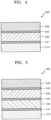
- the optical film 200' may include the 1/4 wavelength ( ⁇ /4) phase retarder 210' and the polarizer 220' sequentially over the display panel 100.
- the optical film 200' may further include a protective base member 230' supporting and protecting the polarizer 220'.
- a pressure sensitive adhesive (PSA) or an adhesive 241' may be between the 1/4 wavelength phase retarder 210' and the polarizer 220'.
- the PSA may be an acryl-based adhesive or a silicon-based adhesive.
- the adhesive may be a polyvinyl alcohol-based adhesive or an epoxy-based adhesive.
- the protective base member 230' may be a cyclo-olefin polymer (COP) film, a tri-acetyl cellulose (TAC) film, or an acrylic film.
- An adhesive 242' may be between the polarizer 220' and the protective base member 230'.
- the adhesive 242' may be a water-based or ultraviolet (UV) adhesive.
- the PSA or adhesive 241' or 242' may be omitted depending on a method of forming the 1/4 wavelength phase retarder 210' and the polarizer 220'.
- the adhesive has adhesion and heat resistance greater than those of the PSA and may have a thickness that is less than that of the PSA.
- the adhesive since the adhesive has a thickness ranging from about 1 ⁇ m to about 5 ⁇ m and has a liquid state, the adhesive may be formed by applying moisture or irradiating light and hardening the liquid adhesive after a coating process.
- the PSA has a thickness ranging from about 5 ⁇ m to about 500 ⁇ m, does not require a coating process, and may be simply formed by only a transfer process. Also, the adhesive cannot be detached after hardening, and when the adhesive is forcibly detached by applying external force, adhesion thereof disappears. On the other hand, the PSA is detachable.
- the 1/4 wavelength phase retarder 210' may be a coated-type phase retarder. That is, the 1/4 wavelength phase retarder 210' may include a reactive liquid crystal.
- the reactive liquid crystal may be a discotic liquid crystal or a nematic liquid crystal.
- the optical film 200' may have a minimized or reduced thickness to facilitate bending or folding. Therefore, the 1/4 wavelength phase retarder 210' may include a coated-type phase retarder having a thickness less than that of a film-type phase retarder.
- the 1/4 wavelength phase retarder 210' may further include an alignment layer for aligning the reactive liquid crystals.
- the polarizer 220' may be polyvinyl acetate (PVA) elongated in a direction (e.g., a predetermined direction) and may transmit only light polarized in a specific direction.
- PVA polyvinyl acetate
- An angle between a slow axis of the 1/4 wavelength phase retarder 210' and an absorption axis of the polarizer 220' may be about 45°, and a combination of the 1/4 wavelength phase retarder 210' and the polarizer 220' may prevent or substantially prevent external light reflection.
- Light incident to the optical film 200' from outside of the display device becomes polarized light by being polarized in a direction (e.g., a predetermined direction) while passing through the polarizer 220', and the polarized light may become circularly polarized light while passing through the 1/4 wavelength phase retarder 210'.
- the circularly polarized light may be reflected to the optical film 200' by the pixel electrode 131, the opposite electrode 135, or a metallic layer of the TFT of the display panel 100.
- FIG. 4 illustrates an example in which the optical film 200' includes only one phase retarder
- the embodiment is not limited thereto. That is, the phase retarder 210' may include a plurality of phase retarders so as to prevent or substantially prevent external light reflection in cooperation with the polarizer 220'.
- a material forming the polarizer 220' may be deformed by the moisture and, thus, at least a portion of the polarizer 220' may lose a function as the polarizer. That is, the polarizer 220' loses a function of transmitting only light polarized in a specific direction and thus the deformed region of the polarizer 220' loses an external light reflection prevention function.
- the first adhesive layer 310 is between the display panel 100 and the optical film 200, and the second adhesive layer 320 is on the optical film 200.
- the first adhesive layer 310 and the second adhesive layer 320 directly contact the first surface 200S1 and the second surface 200S2 opposite the first surface 200S1 of the optical film 200, respectively.
- the optical film 200 is completely surrounded by the first adhesive layer 310 and the second adhesive layer 320. That is, the first adhesive layer 310 and the second adhesive layer 320 seal the optical film 200 in addition to a function of coupling the optical film 200 to a layer under the first adhesive layer 310 and a layer on the second adhesive layer 320.
- external foreign substances such as moisture cannot penetrate into the optical film 200 and, thus, a problem in which the optical film 200 loses the function of preventing external light reflection due to moisture may be reduced or prevented.
- the first adhesive layer 310 and the second adhesive layer 320 include a same material and may have a thickness in a range from about 10 ⁇ m to about 500 ⁇ m. That is, a thickness t 310 of the first adhesive layer 310 and a thickness t 320 of the second adhesive layer 320 may each be in a range from about 10 ⁇ m to about 500 ⁇ m.
- the first adhesive layer 310 and the second adhesive layer 320 may include a PSA as defined above and do not include an adhesive.
- the adhesive requires coating and hardening processes. However, these processes are complicated or performing these processes on the display panel 100 and a window 400 may not be possible.
- the adhesive has a thickness in a range from about 1 ⁇ m to about 5 ⁇ m, it is difficult for the adhesive to cover an end of the optical film 200 and the adhesive cannot planarize a colored layer 500 on an inner surface of the window 400 having a thickness (e.g., a predetermined thickness) as described below.
- the second adhesive layer 320 may have substantially a same area as that of the optical film 200.
- the first adhesive layer 310 may include a protrusion region PR covering an end of the optical film 200 and an end of the second adhesive layer 320. That is, the first adhesive layer 310 may contact the end of the second adhesive layer 320 and seal the optical film 200 in cooperation with the second adhesive layer 320.
- the first adhesive layer 310 including the protrusion region PR may have an area that is greater than that of the optical film 200.
- the protrusion region PR may completely surround a perimeter of the optical film 200 including the end of the optical film 200. Through this configuration, moisture, etc. may not penetrate into the optical film 200. That is, the optical film 200 may be sealed by using the first adhesive layer 310 and the second adhesive layer 320 respectively under and on the optical film 200 without having to perform a separate process of sealing the optical film 200.
- the protrusion region PR may surround a portion of the optical film 200, as described below.
- the window 400 may be on the second adhesive layer 320.
- the window 400 may include transparent glass or plastic and may protect the display panel 100, etc.
- the colored layer 500 having a color may be on the inner surface of the window 400, that is, a surface of the window 400 facing in a direction in which the display panel 100 is arranged.
- the colored layer 500 may have a form of a frame around an edge region of the inner surface of the window 400.
- the colored layer 500 may be a black matrix including a black or an organic material layer having a color (e.g., a predetermined color).
- the colored layer 500 may include a printed letter or a design, for example.
- the first adhesive layer 310 may cover at least a portion of the colored layer 500. That is, the first adhesive layer 310 may include the protrusion region PR protruding from a region arranged under the optical film 200, and the protrusion region PR may cover at least a portion of the colored layer 500.
- a thickness t 500 of the colored layer 500 may be in a range from about 1.0 ⁇ m to about 50 ⁇ m.
- a thickness t PR of the protrusion region PR of the first adhesive layer 310 may be in a range from about 3 times to about 50 times greater than the thickness t 500 of the colored layer 500.
- the optical film 200 may not be completely sealed by the first adhesive layer 310 due to a step difference by the colored layer 500.
- a total thickness of the display device 1 may increase excessively. Due to the excessive increase of the total thickness of the display device 1, in the case in which the display device 1 is implemented as a flexible display device 1, flexibility may be reduced.
- the optical film 200 is sealed by the first adhesive layer 310 and the second adhesive layer 320, moisture does not penetrate into the optical film 200 and a problem in which at least a portion of the polarizer 220 of the optical film 200 loses a function and cannot prevent external light reflection may be prevented or reduced. Therefore, quality of an image produced by the display device 1 may be improved.
- FIG. 5 is a schematic cross-sectional view of a configuration of an optical film of the display device of FIG. 1 .
- An embodiment of the inventive display combines the features of figures 1 with the optical film 200 of figure 5 .
- an optical film 200 includes a 1/4 wavelength phase retarder 210, a 1/2 wavelength phase retarder 250, and a polarizer 220 sequentially (i.e., adjacent to one another) arranged from the display panel 100 (see FIG. 1 ). That is, the optical film 200 of FIG. 5 includes two phase retarders 210 and 250.
- the optical film 200 may further include a protective base member 230 supporting and protecting the polarizer 220.
- APSA or an adhesive 241 or 243 is between the 1/4 wavelength phase retarder 210 and the 1/2 wavelength phase retarder 250 and between the 1/2 wavelength phase retarder 250 and the polarizer 220.
- the PSA may be an acryl-based adhesive or a silicon-based adhesive.
- the adhesive may be a polyvinyl alcohol-based adhesive or an epoxy-based adhesive.
- the protective base member 230 may be a COP film, a TAC film, or an acrylic film.
- An adhesive 242 may be between the polarizer 220 and the protective base member 230.
- the adhesive 242 may be a water-based or UV adhesive.
- the 1/4 wavelength phase retarder 210 and the 1/2 wavelength phase retarder 250 are coated-type phase retarders. That is, the 1/4 wavelength phase retarder 210 includes a reactive liquid crystal.
- the reactive liquid crystal may be a discotic liquid crystal or a nematic liquid crystal.
- the optical film 200 may have a minimized or reduced thickness to facilitate bending or folding. Therefore, the 1/4 wavelength phase retarder 210 and the 1/2 wavelength phase retarder 250 may include a coated-type phase retarder having a thickness that is less than that of a film-type phase retarder.
- the polarizer 220 may be PVA elongated in a direction (e.g., a predetermined direction) and transmit only light polarized in a specific direction.
- an external light reflection prevention performance may deteriorate depending on a wavelength or an angle at which the display device 1 is viewed due to wavelength dependency of the 1/4 wavelength phase retarder 210'.
- the display device 1 is a bendable or foldable display device, since a direction of an optical axis of the 1/4 wavelength phase retarder 210' is changed by tensile force occurring while the display device is bent or folded and an external light reflection prevention performance deteriorates, the color of an image produced by the display device 1 may differ from an intended color.
- the optical film 200 of FIG. 5 includes at least two phase retarders 210 and 250 and the polarizer 220 and may include, for example, the 1/4 wavelength phase retarder 210, the 1/2 wavelength phase retarder 250, and the polarizer 220 sequentially on the display panel 100.
- the 1/2 wavelength phase retarder 250 only changes a polarization direction of polarized light.
- An external light reflection prevention function may be performed by the same principle as that of the optical film 200' including only the 1/4 wavelength phase retarder 210' and the polarizer 220' illustrated in FIG.
- FIG. 6 is a schematic cross-sectional view of a portion of a display device according to another embodiment. Herein, differences between the display device of FIG. 6 and the display device 1 of FIG. 1 are mainly described.
- a display device 2 includes the display panel 100 (see FIG. 1 ) displaying an image, the optical film 200 over the display panel 100, the first adhesive layer 310 between the display panel 100 and the optical film 200 and contacting the first surface 200S1 of the optical film 200, and the second adhesive layer 320 on the optical film 200 and contacting the second surface 200S2 of the optical film 200.
- the first adhesive layer 310 contacts the second adhesive layer 320 and the second adhesive layer 320 comprises a protrusion protruding towards the outside of the optical film 200 and covering an end of the optical film 200.
- An inventive display is formed by combining the features of figure 6 with the optical film 200 of figure 5 .
- various layers such as a touch layer (not shown) between the display panel 100 and the first adhesive layer 310 may be below the first adhesive layer 310.
- layers below the first adhesive layer 310 and contacting the first adhesive layer 310 are referred to as lower layers LL.
- various layers such as a touch layer (not shown) between the second adhesive layer 320 and the window 400 may be over the second adhesive layer 320.
- Layers over the second adhesive layer 320 and contacting the second adhesive layer 320 are referred to as upper layers UL. That is, the lower layers LL and the upper layers UL may be any layers performing various functions as well as an uppermost layer and the window 400 of the display panel 100.
- the window 400 may be a glass window or a film window including plastic.
- the first adhesive layer 310 may have substantially a same area as that of the optical film 200.
- the second adhesive layer 320 may include the protrusion region PR covering an end of the optical film 200 and an end of the first adhesive layer 310. That is, the second adhesive layer 320 may contact an end of the first adhesive layer 310 and seal at least a portion of the optical film 200 in cooperation with the first adhesive layer 310.
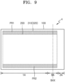
- the protrusion region PR of the second adhesive layer 320 may completely surround a perimeter of the optical film 200, as illustrated in FIG. 2 , or may surround only a portion of a perimeter of the optical film 200, as illustrated in FIGS. 9 and 11 , for example. Through this configuration, a problem in which moisture penetrates into the optical film 200, and thus an external light reflection prevention function of the optical film 200 is lost, may be reduced or prevented.
- the protrusion region PR of the second adhesive layer 320 may extend from the second adhesive layer 320 on the second surface 200S2 of the optical film 200 and contact the lower layers LL under the first adhesive layer 310.
- Thicknesses of the first adhesive layer 310 and the second adhesive layer 320 may have a value in a range from about 10 ⁇ m to about 500 ⁇ m.
- the first adhesive layer 310 and the second adhesive layer 320 may have a thickness about 3 times to about 50 times greater than a height corresponding to a maximum step difference.
- the upper layers UL may be the window 400 (see FIG. 1 ) and the colored layer 500 (see FIG. 1 ) on the inner surface of the window 400.
- the protrusion region PR of the second adhesive layer 320 may have a thickness t PR that is about 3 times to about 50 times greater than the thickness t 500 (see FIG. 1 ) of the colored layer 500.
- FIG. 7 is a schematic cross-sectional view of a portion of a display device according to another embodiment. Herein, differences between the display device of FIG. 7 and the display device 1 of FIG. 1 are mainly described.
- a display device 3 includes the display panel 100 (see FIG. 1 ) displaying an image, the optical film 200 over the display panel 100, the first adhesive layer 310 between the display panel 100 and the optical film 200 and contacting the first surface 200S1 of the optical film 200, and the second adhesive layer 320 on the optical film 200 and contacting the second surface 200S2 of the optical film 200.
- the first adhesive layer 310 contacts the second adhesive layer 320.
- An inventive display is formed when combining the features of figure 7 with the optical film 200 of figure 5 .
- a lower layer LL may be under the first adhesive layer 310.
- the lower layer LL may be an uppermost layer of the display panel 100 or a touch layer (not shown).
- An upper layer UL may be on the second adhesive layer 320.
- the upper layer UL may be the window 400 (see FIG. 1 ) or a touch layer (not shown). That is, the touch layer (not shown) may be on or under the optical film 200.
- the first adhesive layer 310 and the second adhesive layer 320 respectively include protrusion regions PR 310 and PR 320 .
- the protrusion region PR 310 of the first adhesive layer 310 contacts the protrusion region PR 320 of the second adhesive layer 320 at an outer edge of the optical film 200.
- the protrusion region PR 310 of the first adhesive layer 310 and the protrusion region PR 320 of the second adhesive layer 320 each contact at least a portion of the optical film 200 and seal at least a portion of the optical film 200.
- the protrusion region PR 310 of the first adhesive layer 310 and the protrusion region PR 320 of the second adhesive layer 320 may completely surround a perimeter of the optical film 200, as illustrated in FIG. 2 , or may surround a portion of a perimeter of the optical film 200, as illustrated in FIGS. 9 and 11 , for example.
- Thicknesses of the first adhesive layer 310 and the second adhesive layer 320 may have a value in a range from about 10 ⁇ m to about 500 ⁇ m.
- the first adhesive layer 310 and the second adhesive layer 320 may have a thickness about 3 times to about 50 times greater than a height corresponding to a maximum step difference.
- the upper layer UL may include the window 400 (see FIG. 1 ) and the colored layer 500 (see FIG. 1 ) on the inner surface of the window 400.
- the protrusion region PR 320 of the second adhesive layer 320 may have a thickness t PR320 that is about 3 times to about 50 times greater than the thickness t 500 (see FIG. 1 ) of the colored layer 500.
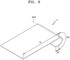
- FIG. 8 is a schematic perspective view of a display device according to another embodiment; and FIG. 9 is a schematic plan view of the display device of FIG. 8 .
- a display device 4 includes the display panel 100 displaying an image, the optical film 200 over the display panel 100, the first adhesive layer 310 between the display panel 100 and the optical film 200, and the second adhesive layer 320 on the optical film 200.
- the first adhesive layer 310 may contact the second adhesive layer 320.
- the display panel 100 includes a first area 1A, a second area 2A, and a bending area BA between the first area 1A and the second area 2A, the bending area being bent or bendable around a bending axis BAX.
- the display panel 100 may include various kinds of display elements over a flexible substrate.
- the first area 1A includes a display area displaying an image.
- the first area 1A may include a portion of a non-display area outside the display area.
- the display area may extend to the bending area BA if desired.
- the bending axis BAX may be defined as an axis corresponding to a central axis of the bending area BA of the display panel 100.
- the optical film 200 may be over at least a portion of the bending area BA.
- the display device 4 may be formed by forming the optical film 200 with the display panel 100 not bent and then bending the display panel 100 and the optical film 200. However, while the optical film 200 is bent, a space between layers of the optical film 200 and/or a layer adjacent to the optical film 200 may be formed, and moisture may penetrate into the optical film 200 via a gap generated by the formed space. A characteristic of the polarizer 220' (see FIG. 4 ) of the optical film may change due to the penetrated moisture and thus at least a portion of the optical film 200' may lose an external light reflection prevention function.
- the optical film 200 may be prevented or substantially prevented by sealing the optical film 200 with the first adhesive layer 310 and the second adhesive layer 320 respectively contacting both surfaces of the optical film 200.
- the first adhesive layer 310 and the second adhesive layer 320 respectively contacting both surfaces of the optical film 200.
- At least one of the first adhesive layer 310 and the second adhesive layer 320 includes protrusion regions PR1 and PR2 covering ends of the optical film 200.
- the protrusion regions PR1 and PR2 may include the first protrusion region PR1 and the second protrusion region PR2 spaced apart from each other in a direction in which the bending axis BAX extends.
- protrusion regions may not be in both edge regions along both directions from the bending axis BAX of the display panel 100, but protrusion regions may be respectively in both other edge regions at least partially included in the bending area BA. That is, since a portion of the optical film 200 in the edge regions not including the bending area BA of the display panel 100 is not bent, moisture may not penetrate into the optical film 200 through this portion. However, since a portion of the optical film 200 in the edge regions including the bending area BA is bent concurrently or simultaneously with the display panel 100, moisture may otherwise easily penetrate into the optical film 200 through this portion. Therefore, at least one of the first adhesive layer 310 and the second adhesive layer 320 in the portion into which moisture otherwise could easily penetrate includes the protrusion regions PR1 and PR2. That is, the first adhesive layer 310 may contact the second adhesive layer 320 in a portion corresponding to the opposite edges that are spaced apart in the direction in which the bending axis BAX extends.
- An inventive display is formed when combining the features of figure 9 with the optical film 200 of figure 5 .
- FIG. 10 is a schematic perspective view of a display device; and FIG. 11 is a schematic plan view of the display device of FIG. 10 .
- a display device 5 is the same as the display device 4 of FIGS. 8 and 9 , except that a short side and a long side of the display panel 100 are changed.
- the first protrusion region PR1 and the second protrusion region PR2 may correspond to both edge regions corresponding to the long side of the display panel 100.
- the first protrusion region PR1 and the second protrusion region PR2 may correspond to both edge regions corresponding to the short side of the display panel 100.
- the display panel 100 of the display device 5 includes the first area 1A, the second area 2A, and the bending area BA between the first area 1A and the second area 2A, the bending area BA being bent or bendable around the bending axis BAX.
- the bending axis BAX may extend in a direction substantially parallel to the long side of the display panel 100. Therefore, penetration of moisture into the optical film 200 may be prevented or reduced by respectively arranging the protrusion regions PR1 and PR2 included in at least one of the first adhesive layer 310 and the second adhesive layer 320 in two edge regions including the bending area BA, and allowing the first adhesive layer 310 to contact the second adhesive layer 320.
- the first protrusion region PR1 and the second protrusion region PR2 may be the protrusion region from the first adhesive layer 310 as illustrated in FIG. 1 , the protrusion region from the second adhesive layer 320 as illustrated in FIG. 6 , or the protrusion regions respectively from the first adhesive layer 310 and the second adhesive layer 320 as illustrated in FIG. 7 .
- a display device may include at least two bending areas. That is, the display panel may have a form including a plurality of regions that are bent. In this case, the edge region corresponding to the bending area of the optical film may be sealed by allowing the first adhesive layer to contact the second adhesive layer.
- the display devices 1, 2, 3, 4, and 5 may prevent or reduce a problem in which moisture penetrates into the optical film 200, at least a portion of the optical film 200 loses an external light reflection prevention function, and in which quality of a produced image is deteriorated.
Landscapes
- Physics & Mathematics (AREA)
- Optics & Photonics (AREA)
- Chemical & Material Sciences (AREA)
- Inorganic Chemistry (AREA)
- Electroluminescent Light Sources (AREA)
Description
- This application claims priority to and the benefit of
Korean Patent Application No. 10-2016-0138641, filed on October 24, 2016 - Aspects of one or more embodiments relate to a display device.
- Generally, a display device includes a display unit over a substrate and displaying an image. At least a portion of the display device may be bent or folded, and thus the display device may be viewed at various angles and portability of the display device may be improved by reducing the volume of the display device.
- Also, the display device may include an optical film which may prevent external light reflection. The optical film may improve visibility and contrast of an image by preventing light incident to the display device from being reflected by a metallic layer, etc. of the display device and being viewed by a user.
- An optical film of a bendable or foldable display device of the related art, preventing external light reflection may receive tensile force or compressive force occurring while the display device is bent or folded. By this force, layers between layers of the optical film and/or adjacent to the optical film are floated, and moisture penetrates into the optical film via the floated region, and thus a polarizer of the optical film is denaturalized. That is, at least a portion of the optical film may not prevent external light reflection and thus quality of an image produced by the display device may deteriorate.
-
US 2016/0293895 A1 discloses a display device including a display panel, a polarizer on the display panel, an adhesion layer on the polarizer, and a window on the adhesion layer, the window including a light transmissive window base, a light shielding layer on the window base and a protrusion on the light shielding layer. -
US 2011/0007391 A1 concerns a display apparatus with protection plate and a manufacturing method thereof. -
US 2012/0012828 A1 concerns an organic light-emitting device including a substrate, an encapsulation substrate, an organic light-emitting unit interposed between the substrate and the encapsulation substrate, and a layer having an UV shielding capability interposed between the encapsulation substrate and the organic light-emitting unit. - According to an aspect of one or more embodiments, a display device has improved quality of a produced image by preventing or reducing penetration of moisture into an optical film. However, this aspect is provided as an example and the scope of the disclosure is not limited thereto.
- Additional aspects will be set forth, in part, in the description which follows and, in part, will be apparent from the description, or may be learned by practice of the presented embodiments.
- According to the invention, a display device comprises the features of
claim 1. According to one or more embodiments, a display device includes: a display panel to display an image; an optical film over the display panel and including at least one phase retarder and a polarizer; a first adhesive layer between the display panel and the optical film and contacting a first surface of the optical film; and a second adhesive layer on the optical film and contacting a second surface of the optical film opposite the first surface, wherein the first adhesive layer and the second adhesive layer contact each other. The at least one phase retarder comprises a 1/4 wavelength phase retarder, and a pressure sensitive adhesive or an adhesive is between the 1/4 wavelength phase retarder and the polarizer, wherein the at least one phase retarder further comprises a 1/2 wavelength phase retarder adjacent to the 1/4 wavelength phase and over the display panel, and the pressure sensitive adhesive or the adhesive is between the 1/4 wavelength phase retarder and the 1/2 wavelength phase retarder and between the 1/2 wavelength phase retarder and the polarizer, wherein the 1/4 wavelength phase retarder includes a reactive liquid crystal, wherein the reactive liquid crystal is a discotic liquid crystal or a nematic liquid crystal. - At least one of the first adhesive layer and the second adhesive layer includes a respective protrusion region protruding toward an outside of the optical film.
- The protrusion region may surround a perimeter of the optical film.
- The display panel may include a bending area bent around a bending axis extending in a direction, at least a portion of the optical film being in the bending area.
- The protrusion region may include a first protrusion region and a second protrusion region spaced apart from each other in the direction in which the bending axis extends.
- The first adhesive layer and the second adhesive layer may include a same material.
- The display panel may include a display area and a non-display area, the display panel having an area greater than that of the optical film, and the optical film completely covering the display area.
- The display device may further include: a window over the optical film; and a colored layer along an edge region of an inner surface of the window.
- At least one of the first adhesive layer and the second adhesive layer may cover at least a portion of the colored layer.
- The protrusion region of the at least one of the first adhesive layer and the second adhesive layer may have a thickness about three times to about fifty times greater than a thickness of the colored layer.
- The second adhesive layer may include the protrusion region, the protrusion region covering an end of the optical film and an end of the first adhesive layer.
- The first adhesive layer may have a same area as that of the optical film.
- The first adhesive layer may include the protrusion region, the protrusion region covering an end of the optical film and an end of the second adhesive layer.
- The second adhesive layer may have a same area as that of the optical film.
- Each of the first adhesive layer and the second adhesive layer may include the protrusion region, the protrusion region of the first adhesive layer contacting the protrusion region of the second adhesive layer at an outer edge of the optical film.
- The display panel may include: a flexible substrate; and an organic light-emitting device over the flexible substrate and including a pixel electrode, an intermediate layer, and an opposite electrode, the intermediate layer including an organic emission layer.
- The display panel may further include: a protective film below the flexible substrate; and an encapsulation layer over the flexible substrate, covering the organic light-emitting device, and including at least one inorganic encapsulation layer and at least one organic encapsulation layer.
- According to one or more embodiments, a display device includes: a display panel to display an image; an optical film over the display panel and including at least one phase retarder and a polarizer; a first adhesive layer between the display panel and the optical film and contacting a first surface of the optical film; and a second adhesive layer on the optical film and contacting a second surface of the optical film opposite the first surface, wherein at least one of the first adhesive layer and the second adhesive layer includes a protrusion region protruding toward an outside of the optical film, and the protrusion region covers an end of the optical film.
- According to one or more embodiments, the display device includes: a display panel according to
claim 1 to display an image and including a bending area bent around a bending axis extending in a direction; and wherein at least a portion of the protrusion region is over the bending area of the display panel. - According to an aspect of one or more embodiments, a display device prevents or reduces quality deterioration of a produced image due to moisture penetrating into an optical film and at least a portion of the optical film losing an external light reflection prevention function. However, the scope of the disclosure is not limited to this effect.
- These and/or other aspects will become apparent and more readily appreciated from the following description of some embodiments, taken in conjunction with the accompanying drawings in which:
-
FIG. 1 is a schematic cross-sectional view of a display; -
FIG. 2 is a schematic plan view of the display device ofFIG. 1 ; -
FIG. 3 is a schematic cross-sectional view of a portion of a display panel of the display device ofFIG. 1 ; -
FIG. 4 is a schematic cross-sectional view of a configuration of an optical film of the display device ofFIG. 1 , according to an embodiment not forming part of the present invention; -
FIG. 5 is a schematic cross-sectional view of a configuration of an optical film of the display device ofFIG. 1 ; -
FIG. 6 is a schematic cross-sectional view of a portion of a display device; -
FIG. 7 is a schematic cross-sectional view of a portion of a display device; -
FIG. 8 is a schematic perspective view of a display device; -
FIG. 9 is a schematic plan view of the display device ofFIG. 8 ; -
FIG. 10 is a schematic perspective view of a display device; and -
FIG. 11 is a schematic plan view of the display device ofFIG. 10 . - An embodiment of an inventive display combines the features of any of
FIGs. 1 ,6 ,7 or9 with the ones ofFIG. 5 . - Although the disclosure allows for various changes and numerous embodiments, some exemplary embodiments will be illustrated in the drawings and described in further detail in the following description. Effects and characteristics of the disclosure, and a method of accomplishing these will be apparent when referring to some embodiments described with reference to the drawings. This disclosure may, however, be embodied in many different forms and should not be construed as limited to the exemplary embodiments set forth herein.
- As used herein, the term "and/or" includes any and all combinations of one or more of the associated listed items.
- Expressions such as "at least one of" when preceding a list of elements, modify the entire list of elements and do not modify the individual elements of the list.
- Hereinafter, the disclosure will be described more fully with reference to the accompanying drawings, in which some exemplary embodiments of the disclosure are shown. When description is made with reference to the drawings, like reference numerals in the drawings denote like or corresponding elements, and repeated description thereof will be omitted.
- It is to be understood that when a layer, region, or component is referred to as being "formed on" another layer, region, or component, it can be directly or indirectly formed on the other layer, region, or component. That is, for example, intervening layers, regions, or components may be present. Sizes of elements in the drawings may be exaggerated for convenience of explanation. In other words, since sizes and thicknesses of components in the drawings may be arbitrarily illustrated for convenience of explanation, embodiments are not limited thereto.
- Hereinafter, some embodiments will be described with reference to the accompanying drawings.
- Referring to
FIGS. 1 to 4 , adisplay device 1 includes adisplay panel 100 displaying an image, anoptical film 200 over thedisplay panel 100 and including at least onephase retarder 210 and apolarizer 220, a firstadhesive layer 310 between thedisplay panel 100 and theoptical film 200 and contacting a first surface 200S1 of theoptical film 200, and a secondadhesive layer 320 on theoptical film 200 and contacting a second surface 200S2 of theoptical film 200, the firstadhesive layer 310 contacting the secondadhesive layer 320. - With reference to
FIG. 3 , thedisplay panel 100 may include asubstrate 120 and an organic light-emitting device (OLED) 130 over thesubstrate 120. Thesubstrate 120 may be a flexible substrate. For example, thesubstrate 120 may include a polymer resin, such as polyethersulfone (PES), polyacrylate (PAR), polyetherimide (PEI), polyethylene naphthalate (PEN), polyethylene terephthalate (PET), polyphenylene sulfide (PPS), polyallylate, polyimide (PI), polycarbonate (PC), or cellulose acetate propionate (CAP). - A thin film transistor (TFT) electrically connected to the
OLED 130 may be over thesubstrate 120. The TFT may include asemiconductor layer 122 including amorphous silicon, polycrystalline silicon, or an organic semiconductor material, agate electrode 124, asource electrode 126S, and adrain electrode 126D. To secure insulation between thesemiconductor layer 122 and thegate electrode 124, agate insulating layer 123 may be between thesemiconductor layer 122 and thegate electrode 124, thegate insulating layer 123 including an inorganic material, such as silicon oxide, silicon nitride, and/or silicon oxynitride. An interlayer insulatinglayer 125 may be on thegate electrode 124, theinterlayer insulating layer 125 including an inorganic material, such as silicon oxide, silicon nitride, and/or silicon oxynitride. The source electrode 126S and thedrain electrode 126D may be on theinterlayer insulating layer 125. The insulating layers including an inorganic material may be formed by chemical vapor deposition (CVD) or atomic layer deposition (ALD). - A
buffer layer 121 may be between thesubstrate 120 and the TFT having the above structure, thebuffer layer 121 including an inorganic material, such as silicon oxide, silicon nitride, and/or silicon oxynitride. Thebuffer layer 121 may increase planarization of the upper surface of thesubstrate 120, or prevent or minimize penetration of impurities from thesubstrate 120 into thesemiconductor layer 122 of the TFT. - A
planarization layer 127 may be on the TFT. For example, in the case where theOLED 130 is over the TFT, theplanarization layer 127 may substantially planarize the TFT. Theplanarization layer 127 may include an organic material, such as PI, benzocyclobutene (BCB), or hexamethyldisiloxane (HMDSO). Although theplanarization layer 127 is shown as a single layer inFIG. 3 , theplanarization layer 127 may be a multi-layer and variously selected. TheOLED 130 may be on theplanarization layer 127, theOLED 130 including apixel electrode 131, anopposite electrode 135, and anintermediate layer 133 between thepixel electrode 131 and theopposite electrode 135, theintermediate layer 133 including an emission layer. Thepixel electrode 131 is electrically connected to the TFT by contacting one of thesource electrode 126S and thedrain electrode 126D via an opening of theplanarization layer 127. - The
pixel electrode 131 may be a reflective electrode including a reflective layer. For example, the reflective layer may include at least one of Ag, Mg, Al, Pt, Pd, Au, Ni, Nd, Ir, and Cr. A transparent or semi-transparent electrode layer may be further over the reflective layer, the transparent or semi-transparent electrode layer including at least one of indium tin oxide (ITO), indium zinc oxide (IZO), zinc oxide (ZnO), indium oxide (In2O3), indium gallium oxide (IGO), and aluminum zinc oxide (AZO). - The
pixel electrode 131 may include three layers including ITO/Ag/ITO. - A pixel-defining
layer 129 may be on theplanarization layer 127. The pixel-defininglayer 129 defines a pixel by including an opening corresponding to each subpixel, that is, an opening exposing at least a central portion of thepixel electrode 131. The pixel-defininglayer 129 may prevent an arc, etc. from occurring at an edge of thepixel electrode 131 by increasing a distance between the edge of thepixel electrode 131 and theopposite electrode 135 over thepixel electrode 131. The pixel-defininglayer 129 may include an organic material, such as PI or HMDSO. - The
intermediate layer 133 of theOLED 130 may include an organic emission layer. In addition, theintermediate layer 133 may further include at least one of a hole injection layer (HIL), a hole transport layer (HTL), an electron transport layer (ETL), and an electron injection layer (EIL). However, the embodiment is not limited thereto and theintermediate layer 133 may further include any of various functional layers. - The
intermediate layer 133 is not limited to the above described layers and may have any of various structures. Also, theintermediate layer 133 may include a layer which is one body over a plurality ofpixel electrodes 131 or include a layer patterned to respectively correspond to thepixel electrodes 131. - To emit white light, the organic emission layer may have a multi-layered structure in which a red emission layer, a green emission layer, and a blue emission layer are stacked, or may have a single-layered structure including a red emission material, a green emission material, and a blue emission material. The
OLED 130 including the organic emission layer may emit full colors by additionally including a red color filter, a green color filter, and a blue color filter. - The
opposite electrode 135 may be a (semi)-transparent electrode. For example, theopposite electrode 135 may include at least one of Ag, Al, Mg, Li, Ca, Cu, LiF/Ca, MgAg, and CaAg. Theopposite electrode 135 may include a thin layer which may transmit light, the thin layer having a thickness in a range from about several nm to about tens of nm. - Since the OLED may be easily damaged by external moisture or oxygen, an
encapsulation layer 140 may cover and protect the OLED. Theencapsulation layer 140 may include a firstinorganic encapsulation layer 141, anorganic encapsulation layer 142, and a secondinorganic encapsulation layer 143. - The first
inorganic encapsulation layer 141 may cover theopposite electrode 135 and include silicon oxide, silicon nitride, and/or silicon oxynitride. When needed, one or more other layers, such as a capping layer or a LiF layer, may be between the firstinorganic encapsulation layer 141 and theopposite electrode 135. Since the firstinorganic encapsulation layer 141 is along a structure therebeneath, the upper surface of the firstinorganic encapsulation layer 141 is not planarized, as illustrated inFIG. 3 . Theorganic encapsulation layer 142 may cover the firstinorganic encapsulation layer 141. Unlike the firstinorganic encapsulation layer 141, the upper surface of theorganic encapsulation layer 142 may be planarized. Theorganic encapsulation layer 142 may include at least one of PET, PEN, PC, PI, polyethylene sulfonate, polyoxymethylene, polyallylate, and HMDSO. The secondinorganic encapsulation layer 143 may cover theorganic encapsulation layer 142 and include silicon oxide, silicon nitride, and/or silicon oxynitride. The secondinorganic encapsulation layer 143 may prevent theorganic encapsulation layer 142 from being exposed to the outside by contacting the firstinorganic encapsulation layer 141 in an edge region of thedisplay panel 100. - As described above, the
encapsulation layer 140 includes the firstinorganic encapsulation layer 141, theorganic encapsulation layer 142, and the secondinorganic encapsulation layer 143. Through the above multi-layered structure, even when a crack occurs inside theencapsulation layer 140, the crack may not be connected between the firstinorganic encapsulation layer 141 and theorganic encapsulation layer 142 or between theorganic encapsulation layer 142 and the secondinorganic encapsulation layer 143. Through this structure, forming of a path via which external moisture or oxygen penetrates into theOLED 130 may be prevented or reduced. - The
display panel 100 includes aprotective film 110 on a lower surface of thesubstrate 120, which is a surface in an opposite direction to a direction in which theOLED 130 is arranged. Theprotective film 110 may include PET or PI. Theprotective film 110 may be attached to the lower surface of thesubstrate 120 by using an adhesive layer (not shown). - For example, in a case of forming a plurality of display units over one parent substrate, to facilitate handling of the parent substrate having a flexible or bendable characteristic during a manufacturing process, a hard carrier substrate may be below the parent substrate. With the parent substrate supported by the carrier substrate, a circuit portion including a TFT, a plurality of
OLEDs 130, and theencapsulation layer 140 encapsulating them are formed over the parent substrate. After theOLEDs 130 are formed over the parent substrate, the carrier substrate may be separated from the parent substrate. Also, after a touch electrode and/or a touch protective layer for protecting the touch electrode are formed, the carrier substrate may be separated from the parent substrate. In any case, a plurality ofdisplay panels 100 may be obtained by, after separating the carrier substrate from the parent substrate, attaching theprotective film 110 on a surface of the parent substrate, and then cutting the parent substrate and the protective film. Thesubstrate 120 may be understood as meaning the above-described cut parent substrate. - After the
display panels 100 are obtained by cutting the parent substrate and theprotective film 110, theoptical film 200 may be attached to theencapsulation layer 140. If a touch electrode or a touch protective layer is over theencapsulation layer 140, theoptical film 200 is over these elements. - Also, the
display panels 100 may not be simultaneously obtained by using the parent substrate, and one display unit may be formed over onesubstrate 120. Even in this case, to facilitate handling of thesubstrate 120 having a flexible characteristic during a manufacturing process, a hard carrier substrate may be below thesubstrate 120. After a display element such as theOLED 130, a circuit portion including a TFT, and theencapsulation layer 140 encapsulating them are formed over thesubstrate 120, the carrier substrate may be separated from thesubstrate 120. Also, after a touch electrode and/or a touch protective layer for protecting the touch electrode are formed over theencapsulation layer 140, the carrier substrate may be separated from thesubstrate 120. - In any case, after the carrier substrate is separated from the parent substrate, the
protective film 110 may be attached on a lower surface of thesubstrate 120. After that, theoptical film 200 may be attached on theencapsulation layer 140 or the touch protective layer, and, if needed, a printed circuit substrate (not shown) or an electronic chip (not shown) may be attached to an edge region of thedisplay panel 100. - Although
FIG. 3 illustrates a case in which thedisplay panel 100 has a flexible characteristic, embodiments are not limited thereto. For example, in another embodiment, thesubstrate 120 of thedisplay panel 100 may not have a flexible characteristic and may be a rigid substrate including any of various materials, such as glass or metal. In an embodiment, theprotective film 110 may be omitted. - The
display panel 100 includes a display area DA displaying an image and a non-display area NA outside the display area DA and not displaying an image. A plurality of pixels is in the display area DA and may produce an image through a combination of light emitted respectively from the pixels. Wirings transferring signals to the pixels, and a circuit portion and a pad portion controlling electrical signals applied to the display area DA may be in the non-display area NA. - The
optical film 200 is over thedisplay panel 100. Theoptical film 200 may cover at least the display area DA of thedisplay panel 100. As illustrated inFIG. 2 , thedisplay panel 100 may have an area that is greater than that of theoptical film 200. For example, theoptical film 200 may be manufactured less than thedisplay panel 100 by taking into account an alignment tolerance while theoptical film 200 is attached to thedisplay panel 100. A distance between an end of thedisplay panel 100 and an end of theoptical film 200 may be from about 0.5 mm to about 2 mm. - The
optical film 200 may improve visibility of thedisplay device 1 by preventing or substantially preventing external light reflection. If theoptical film 200 does not cover a portion of the display area DA, visibility of thedisplay device 1 may deteriorate. Therefore, in an embodiment, theoptical film 200 may completely cover the display area DA. - Referring to
FIG. 4 , the optical film 200' according to an embodiment not forming part of the present invention may include the 1/4 wavelength (λ/4) phase retarder 210' and the polarizer 220' sequentially over thedisplay panel 100. The optical film 200' may further include a protective base member 230' supporting and protecting the polarizer 220'. A pressure sensitive adhesive (PSA) or an adhesive 241' may be between the 1/4 wavelength phase retarder 210' and the polarizer 220'. For example, the PSA may be an acryl-based adhesive or a silicon-based adhesive. The adhesive may be a polyvinyl alcohol-based adhesive or an epoxy-based adhesive. The protective base member 230' may be a cyclo-olefin polymer (COP) film, a tri-acetyl cellulose (TAC) film, or an acrylic film. An adhesive 242' may be between the polarizer 220' and the protective base member 230'. The adhesive 242' may be a water-based or ultraviolet (UV) adhesive. The PSA or adhesive 241' or 242' may be omitted depending on a method of forming the 1/4 wavelength phase retarder 210' and the polarizer 220'. - The PSA and the adhesive are described further below. That is, the adhesive has adhesion and heat resistance greater than those of the PSA and may have a thickness that is less than that of the PSA. For example, since the adhesive has a thickness ranging from about 1 µm to about 5 µm and has a liquid state, the adhesive may be formed by applying moisture or irradiating light and hardening the liquid adhesive after a coating process. In contrast, the PSA has a thickness ranging from about 5 µm to about 500 µm, does not require a coating process, and may be simply formed by only a transfer process. Also, the adhesive cannot be detached after hardening, and when the adhesive is forcibly detached by applying external force, adhesion thereof disappears. On the other hand, the PSA is detachable.
- According to this embodiment, the 1/4 wavelength phase retarder 210' may be a coated-type phase retarder. That is, the 1/4 wavelength phase retarder 210' may include a reactive liquid crystal. The reactive liquid crystal may be a discotic liquid crystal or a nematic liquid crystal. In the case in which the display device has a flexible characteristic, the optical film 200' may have a minimized or reduced thickness to facilitate bending or folding. Therefore, the 1/4 wavelength phase retarder 210' may include a coated-type phase retarder having a thickness less than that of a film-type phase retarder. Though not shown, in addition to the reactive liquid crystal, the 1/4 wavelength phase retarder 210' may further include an alignment layer for aligning the reactive liquid crystals.
- The polarizer 220' may be polyvinyl acetate (PVA) elongated in a direction (e.g., a predetermined direction) and may transmit only light polarized in a specific direction.
- An angle between a slow axis of the 1/4 wavelength phase retarder 210' and an absorption axis of the polarizer 220' may be about 45°, and a combination of the 1/4 wavelength phase retarder 210' and the polarizer 220' may prevent or substantially prevent external light reflection. Light incident to the optical film 200' from outside of the display device becomes polarized light by being polarized in a direction (e.g., a predetermined direction) while passing through the polarizer 220', and the polarized light may become circularly polarized light while passing through the 1/4 wavelength phase retarder 210'. The circularly polarized light may be reflected to the optical film 200' by the
pixel electrode 131, theopposite electrode 135, or a metallic layer of the TFT of thedisplay panel 100. - When light is reflected by a metallic layer, etc., circularly polarized light in a clockwise direction is converted into circularly polarized light in a counterclockwise direction, and circularly polarized light in a counterclockwise direction is converted into circularly polarized light in a clockwise direction. Light of which the rotation direction has been converted becomes light polarized in a direction (e.g., a predetermined direction) while passing through the 1/4 wavelength phase retarder 210'. However, a polarization direction of light which has passed through the 1/4 wavelength phase retarder 210' after reflection is different, by about 90°, from a polarization direction of light incident to the 1/4 wavelength phase retarder 210' before reflection. Therefore, incident external light is not emitted to an outside of the display device and thus is not visible to a user. By this, visibility and contrast of the
display device 1 may be improved. - Although
FIG. 4 illustrates an example in which the optical film 200' includes only one phase retarder, the embodiment is not limited thereto. That is, the phase retarder 210' may include a plurality of phase retarders so as to prevent or substantially prevent external light reflection in cooperation with the polarizer 220'. - In a case in which moisture penetrates into the polarizer 220' of the optical film 200', a material forming the polarizer 220' may be deformed by the moisture and, thus, at least a portion of the polarizer 220' may lose a function as the polarizer. That is, the polarizer 220' loses a function of transmitting only light polarized in a specific direction and thus the deformed region of the polarizer 220' loses an external light reflection prevention function.
- As illustrated in
FIG. 1 , the firstadhesive layer 310 is between thedisplay panel 100 and theoptical film 200, and the secondadhesive layer 320 is on theoptical film 200. The firstadhesive layer 310 and the secondadhesive layer 320 directly contact the first surface 200S1 and the second surface 200S2 opposite the first surface 200S1 of theoptical film 200, respectively. - The
optical film 200 is completely surrounded by the firstadhesive layer 310 and the secondadhesive layer 320. That is, the firstadhesive layer 310 and the secondadhesive layer 320 seal theoptical film 200 in addition to a function of coupling theoptical film 200 to a layer under the firstadhesive layer 310 and a layer on the secondadhesive layer 320. Through this configuration, external foreign substances such as moisture cannot penetrate into theoptical film 200 and, thus, a problem in which theoptical film 200 loses the function of preventing external light reflection due to moisture may be reduced or prevented. - The first
adhesive layer 310 and the secondadhesive layer 320 include a same material and may have a thickness in a range from about 10 µm to about 500 µm. That is, a thickness t310 of the firstadhesive layer 310 and a thickness t320 of the secondadhesive layer 320 may each be in a range from about 10 µm to about 500 µm. In an embodiment, the firstadhesive layer 310 and the secondadhesive layer 320 may include a PSA as defined above and do not include an adhesive. The adhesive requires coating and hardening processes. However, these processes are complicated or performing these processes on thedisplay panel 100 and awindow 400 may not be possible. Also, since the adhesive has a thickness in a range from about 1 µm to about 5 µm, it is difficult for the adhesive to cover an end of theoptical film 200 and the adhesive cannot planarize acolored layer 500 on an inner surface of thewindow 400 having a thickness (e.g., a predetermined thickness) as described below. - The second
adhesive layer 320 may have substantially a same area as that of theoptical film 200. The firstadhesive layer 310 may include a protrusion region PR covering an end of theoptical film 200 and an end of the secondadhesive layer 320. That is, the firstadhesive layer 310 may contact the end of the secondadhesive layer 320 and seal theoptical film 200 in cooperation with the secondadhesive layer 320. - The first
adhesive layer 310 including the protrusion region PR may have an area that is greater than that of theoptical film 200. The protrusion region PR may completely surround a perimeter of theoptical film 200 including the end of theoptical film 200. Through this configuration, moisture, etc. may not penetrate into theoptical film 200. That is, theoptical film 200 may be sealed by using the firstadhesive layer 310 and the secondadhesive layer 320 respectively under and on theoptical film 200 without having to perform a separate process of sealing theoptical film 200. However, embodiments are not limited thereto. The protrusion region PR may surround a portion of theoptical film 200, as described below. - The
window 400 may be on the secondadhesive layer 320. Thewindow 400 may include transparent glass or plastic and may protect thedisplay panel 100, etc. - The
colored layer 500 having a color (e.g., a predetermined color) may be on the inner surface of thewindow 400, that is, a surface of thewindow 400 facing in a direction in which thedisplay panel 100 is arranged. Thecolored layer 500 may have a form of a frame around an edge region of the inner surface of thewindow 400. For example, thecolored layer 500 may be a black matrix including a black or an organic material layer having a color (e.g., a predetermined color). Thecolored layer 500 may include a printed letter or a design, for example. - The first
adhesive layer 310 may cover at least a portion of thecolored layer 500. That is, the firstadhesive layer 310 may include the protrusion region PR protruding from a region arranged under theoptical film 200, and the protrusion region PR may cover at least a portion of thecolored layer 500. For example, a thickness t500 of thecolored layer 500 may be in a range from about 1.0 µm to about 50 µm. A thickness tPR of the protrusion region PR of the firstadhesive layer 310 may be in a range from about 3 times to about 50 times greater than the thickness t500 of thecolored layer 500. When the thickness tPR of the protrusion region PR of the firstadhesive layer 310 is less than the lower value of the above-described range, theoptical film 200 may not be completely sealed by the firstadhesive layer 310 due to a step difference by thecolored layer 500. When the thickness tPR of the protrusion region PR of the firstadhesive layer 310 is greater than the upper value of the above-described range, a total thickness of thedisplay device 1 may increase excessively. Due to the excessive increase of the total thickness of thedisplay device 1, in the case in which thedisplay device 1 is implemented as aflexible display device 1, flexibility may be reduced. - As described above, since the
optical film 200 is sealed by the firstadhesive layer 310 and the secondadhesive layer 320, moisture does not penetrate into theoptical film 200 and a problem in which at least a portion of thepolarizer 220 of theoptical film 200 loses a function and cannot prevent external light reflection may be prevented or reduced. Therefore, quality of an image produced by thedisplay device 1 may be improved. -
FIG. 5 is a schematic cross-sectional view of a configuration of an optical film of the display device ofFIG. 1 , An embodiment of the inventive display combines the features offigures 1 with theoptical film 200 offigure 5 . - Referring to
FIG. 5 , anoptical film 200 according to an embodiment includes a 1/4wavelength phase retarder 210, a 1/2wavelength phase retarder 250, and apolarizer 220 sequentially (i.e., adjacent to one another) arranged from the display panel 100 (seeFIG. 1 ). That is, theoptical film 200 ofFIG. 5 includes twophase retarders optical film 200 may further include aprotective base member 230 supporting and protecting thepolarizer 220. APSA or an adhesive 241 or 243 is between the 1/4wavelength phase retarder 210 and the 1/2wavelength phase retarder 250 and between the 1/2wavelength phase retarder 250 and thepolarizer 220. For example, the PSA may be an acryl-based adhesive or a silicon-based adhesive. The adhesive may be a polyvinyl alcohol-based adhesive or an epoxy-based adhesive. Theprotective base member 230 may be a COP film, a TAC film, or an acrylic film. An adhesive 242 may be between thepolarizer 220 and theprotective base member 230. The adhesive 242 may be a water-based or UV adhesive. - The 1/4
wavelength phase retarder 210 and the 1/2wavelength phase retarder 250 are coated-type phase retarders. That is, the 1/4wavelength phase retarder 210 includes a reactive liquid crystal. The reactive liquid crystal may be a discotic liquid crystal or a nematic liquid crystal. In the case in which the display device has a flexible characteristic, theoptical film 200 may have a minimized or reduced thickness to facilitate bending or folding. Therefore, the 1/4wavelength phase retarder 210 and the 1/2wavelength phase retarder 250 may include a coated-type phase retarder having a thickness that is less than that of a film-type phase retarder. - The
polarizer 220 may be PVA elongated in a direction (e.g., a predetermined direction) and transmit only light polarized in a specific direction. - As illustrated in
FIG. 4 , in the case in which the optical film 200' includes only one 1/4 wavelength phase retarder 210', an external light reflection prevention performance may deteriorate depending on a wavelength or an angle at which thedisplay device 1 is viewed due to wavelength dependency of the 1/4 wavelength phase retarder 210'. Also, in the case in which thedisplay device 1 is a bendable or foldable display device, since a direction of an optical axis of the 1/4 wavelength phase retarder 210' is changed by tensile force occurring while the display device is bent or folded and an external light reflection prevention performance deteriorates, the color of an image produced by thedisplay device 1 may differ from an intended color. - The
optical film 200 ofFIG. 5 includes at least twophase retarders polarizer 220 and may include, for example, the 1/4wavelength phase retarder 210, the 1/2wavelength phase retarder 250, and thepolarizer 220 sequentially on thedisplay panel 100. The 1/2wavelength phase retarder 250 only changes a polarization direction of polarized light. An external light reflection prevention function may be performed by the same principle as that of the optical film 200' including only the 1/4 wavelength phase retarder 210' and the polarizer 220' illustrated inFIG. 4 , and a problem in which the external light reflection prevention performance changes depending on a wavelength and an angle at which the display device is viewed, may be minimized or reduced by properly setting an angle between an absorption axis of thepolarizer 220 and optical axes of the 1/4wavelength phase retarder 210 and the 1/2wavelength phase retarder 250. -
FIG. 6 is a schematic cross-sectional view of a portion of a display device according to another embodiment. Herein, differences between the display device ofFIG. 6 and thedisplay device 1 ofFIG. 1 are mainly described. - Referring to
FIG. 6 , adisplay device 2 according to another embodiment includes the display panel 100 (seeFIG. 1 ) displaying an image, theoptical film 200 over thedisplay panel 100, the firstadhesive layer 310 between thedisplay panel 100 and theoptical film 200 and contacting the first surface 200S1 of theoptical film 200, and the secondadhesive layer 320 on theoptical film 200 and contacting the second surface 200S2 of theoptical film 200. The firstadhesive layer 310 contacts the secondadhesive layer 320 and the secondadhesive layer 320 comprises a protrusion protruding towards the outside of theoptical film 200 and covering an end of theoptical film 200. - An inventive display is formed by combining the features of
figure 6 with theoptical film 200 offigure 5 . - Besides the
display panel 100, various layers such as a touch layer (not shown) between thedisplay panel 100 and the firstadhesive layer 310 may be below the firstadhesive layer 310. InFIG. 6 , layers below the firstadhesive layer 310 and contacting the firstadhesive layer 310 are referred to as lower layers LL. Likewise, besides the window 400 (seeFIG. 1 ), various layers such as a touch layer (not shown) between the secondadhesive layer 320 and thewindow 400 may be over the secondadhesive layer 320. Layers over the secondadhesive layer 320 and contacting the secondadhesive layer 320 are referred to as upper layers UL. That is, the lower layers LL and the upper layers UL may be any layers performing various functions as well as an uppermost layer and thewindow 400 of thedisplay panel 100. In an embodiment, thewindow 400 may be a glass window or a film window including plastic. - The first
adhesive layer 310 may have substantially a same area as that of theoptical film 200. The secondadhesive layer 320 may include the protrusion region PR covering an end of theoptical film 200 and an end of the firstadhesive layer 310. That is, the secondadhesive layer 320 may contact an end of the firstadhesive layer 310 and seal at least a portion of theoptical film 200 in cooperation with the firstadhesive layer 310. The protrusion region PR of the secondadhesive layer 320 may completely surround a perimeter of theoptical film 200, as illustrated inFIG. 2 , or may surround only a portion of a perimeter of theoptical film 200, as illustrated inFIGS. 9 and11 , for example. Through this configuration, a problem in which moisture penetrates into theoptical film 200, and thus an external light reflection prevention function of theoptical film 200 is lost, may be reduced or prevented. - The protrusion region PR of the second
adhesive layer 320 may extend from the secondadhesive layer 320 on the second surface 200S2 of theoptical film 200 and contact the lower layers LL under the firstadhesive layer 310. - Thicknesses of the first
adhesive layer 310 and the secondadhesive layer 320 may have a value in a range from about 10 µm to about 500 µm. In a case in which the lower layers LL and the upper layers UL include a step difference, the firstadhesive layer 310 and the secondadhesive layer 320 may have a thickness about 3 times to about 50 times greater than a height corresponding to a maximum step difference. For example, the upper layers UL may be the window 400 (seeFIG. 1 ) and the colored layer 500 (seeFIG. 1 ) on the inner surface of thewindow 400. The protrusion region PR of the secondadhesive layer 320 may have a thickness tPR that is about 3 times to about 50 times greater than the thickness t500 (seeFIG. 1 ) of thecolored layer 500. -
FIG. 7 is a schematic cross-sectional view of a portion of a display device according to another embodiment. Herein, differences between the display device ofFIG. 7 and thedisplay device 1 ofFIG. 1 are mainly described. - Referring to
FIG. 7 , adisplay device 3 according to another embodiment includes the display panel 100 (seeFIG. 1 ) displaying an image, theoptical film 200 over thedisplay panel 100, the firstadhesive layer 310 between thedisplay panel 100 and theoptical film 200 and contacting the first surface 200S1 of theoptical film 200, and the secondadhesive layer 320 on theoptical film 200 and contacting the second surface 200S2 of theoptical film 200. The firstadhesive layer 310 contacts the secondadhesive layer 320. An inventive display is formed when combining the features offigure 7 with theoptical film 200 offigure 5 . - A lower layer LL may be under the first
adhesive layer 310. For example, the lower layer LL may be an uppermost layer of thedisplay panel 100 or a touch layer (not shown). An upper layer UL may be on the secondadhesive layer 320. For example, the upper layer UL may be the window 400 (seeFIG. 1 ) or a touch layer (not shown). That is, the touch layer (not shown) may be on or under theoptical film 200. - According to this embodiment, the first
adhesive layer 310 and the secondadhesive layer 320 respectively include protrusion regions PR310 and PR320. The protrusion region PR310 of the firstadhesive layer 310 contacts the protrusion region PR320 of the secondadhesive layer 320 at an outer edge of theoptical film 200. - That is, the protrusion region PR310 of the first
adhesive layer 310 and the protrusion region PR320 of the secondadhesive layer 320 each contact at least a portion of theoptical film 200 and seal at least a portion of theoptical film 200. The protrusion region PR310 of the firstadhesive layer 310 and the protrusion region PR320 of the secondadhesive layer 320 may completely surround a perimeter of theoptical film 200, as illustrated inFIG. 2 , or may surround a portion of a perimeter of theoptical film 200, as illustrated inFIGS. 9 and11 , for example. Through this configuration, a problem in which moisture penetrates into theoptical film 200, and thus an external light reflection prevention function of theoptical film 200 is lost, may be reduced or prevented. - Thicknesses of the first
adhesive layer 310 and the secondadhesive layer 320 may have a value in a range from about 10 µm to about 500 µm. In a case in which the lower layer LL and the upper layer UL include a step difference, the firstadhesive layer 310 and the secondadhesive layer 320 may have a thickness about 3 times to about 50 times greater than a height corresponding to a maximum step difference. For example, the upper layer UL may include the window 400 (seeFIG. 1 ) and the colored layer 500 (seeFIG. 1 ) on the inner surface of thewindow 400. The protrusion region PR320 of the secondadhesive layer 320 may have a thickness tPR320 that is about 3 times to about 50 times greater than the thickness t500 (seeFIG. 1 ) of thecolored layer 500. -
FIG. 8 is a schematic perspective view of a display device according to another embodiment; andFIG. 9 is a schematic plan view of the display device ofFIG. 8 . - Referring to
FIGS. 8 and9 , adisplay device 4 according to another embodiment includes thedisplay panel 100 displaying an image, theoptical film 200 over thedisplay panel 100, the firstadhesive layer 310 between thedisplay panel 100 and theoptical film 200, and the secondadhesive layer 320 on theoptical film 200. The firstadhesive layer 310 may contact the secondadhesive layer 320. - The
display panel 100 includes afirst area 1A, asecond area 2A, and a bending area BA between thefirst area 1A and thesecond area 2A, the bending area being bent or bendable around a bending axis BAX. For example, thedisplay panel 100 may include various kinds of display elements over a flexible substrate. In an embodiment, thefirst area 1A includes a display area displaying an image. In addition to the display area, thefirst area 1A may include a portion of a non-display area outside the display area. The display area may extend to the bending area BA if desired. Here, the bending axis BAX may be defined as an axis corresponding to a central axis of the bending area BA of thedisplay panel 100. - The
optical film 200 may be over at least a portion of the bending area BA. Thedisplay device 4 may be formed by forming theoptical film 200 with thedisplay panel 100 not bent and then bending thedisplay panel 100 and theoptical film 200. However, while theoptical film 200 is bent, a space between layers of theoptical film 200 and/or a layer adjacent to theoptical film 200 may be formed, and moisture may penetrate into theoptical film 200 via a gap generated by the formed space. A characteristic of the polarizer 220' (seeFIG. 4 ) of the optical film may change due to the penetrated moisture and thus at least a portion of the optical film 200' may lose an external light reflection prevention function. - However, penetration of moisture, etc. into the
optical film 200 may be prevented or substantially prevented by sealing theoptical film 200 with the firstadhesive layer 310 and the secondadhesive layer 320 respectively contacting both surfaces of theoptical film 200. As described above, since moisture may otherwise easily penetrate into theoptical film 200 while theoptical film 200 is bent, a portion of theoptical film 200 corresponding to an area of theoptical film 200 where a space between layers may be formed while theoptical film 200 is bent is sealed. - As illustrated in
FIG. 9 , at least one of the firstadhesive layer 310 and the secondadhesive layer 320 includes protrusion regions PR1 and PR2 covering ends of theoptical film 200. The protrusion regions PR1 and PR2 may include the first protrusion region PR1 and the second protrusion region PR2 spaced apart from each other in a direction in which the bending axis BAX extends. - In an embodiment, protrusion regions may not be in both edge regions along both directions from the bending axis BAX of the
display panel 100, but protrusion regions may be respectively in both other edge regions at least partially included in the bending area BA. That is, since a portion of theoptical film 200 in the edge regions not including the bending area BA of thedisplay panel 100 is not bent, moisture may not penetrate into theoptical film 200 through this portion. However, since a portion of theoptical film 200 in the edge regions including the bending area BA is bent concurrently or simultaneously with thedisplay panel 100, moisture may otherwise easily penetrate into theoptical film 200 through this portion. Therefore, at least one of the firstadhesive layer 310 and the secondadhesive layer 320 in the portion into which moisture otherwise could easily penetrate includes the protrusion regions PR1 and PR2. That is, the firstadhesive layer 310 may contact the secondadhesive layer 320 in a portion corresponding to the opposite edges that are spaced apart in the direction in which the bending axis BAX extends. - Through this configuration, penetration of moisture into the
optical film 200 may be prevented or reduced. An inventive display is formed when combining the features offigure 9 with theoptical film 200 offigure 5 . -
FIG. 10 is a schematic perspective view of a display device; andFIG. 11 is a schematic plan view of the display device ofFIG. 10 . - Referring to
FIGS. 10 and11 , adisplay device 5 is the same as thedisplay device 4 ofFIGS. 8 and9 , except that a short side and a long side of thedisplay panel 100 are changed. - That is, in the
display device 4 ofFIGS. 8 and9 , the first protrusion region PR1 and the second protrusion region PR2 may correspond to both edge regions corresponding to the long side of thedisplay panel 100. In contrast, in thedisplay device 5 ofFIGS. 10 and11 , the first protrusion region PR1 and the second protrusion region PR2 may correspond to both edge regions corresponding to the short side of thedisplay panel 100. - That is, the
display panel 100 of thedisplay device 5 includes thefirst area 1A, thesecond area 2A, and the bending area BA between thefirst area 1A and thesecond area 2A, the bending area BA being bent or bendable around the bending axis BAX. The bending axis BAX may extend in a direction substantially parallel to the long side of thedisplay panel 100. Therefore, penetration of moisture into theoptical film 200 may be prevented or reduced by respectively arranging the protrusion regions PR1 and PR2 included in at least one of the firstadhesive layer 310 and the secondadhesive layer 320 in two edge regions including the bending area BA, and allowing the firstadhesive layer 310 to contact the secondadhesive layer 320. - The first protrusion region PR1 and the second protrusion region PR2 may be the protrusion region from the first
adhesive layer 310 as illustrated inFIG. 1 , the protrusion region from the secondadhesive layer 320 as illustrated inFIG. 6 , or the protrusion regions respectively from the firstadhesive layer 310 and the secondadhesive layer 320 as illustrated inFIG. 7 . - Though not shown, a display device according to an embodiment may include at least two bending areas. That is, the display panel may have a form including a plurality of regions that are bent. In this case, the edge region corresponding to the bending area of the optical film may be sealed by allowing the first adhesive layer to contact the second adhesive layer.
- The
display devices optical film 200, at least a portion of theoptical film 200 loses an external light reflection prevention function, and in which quality of a produced image is deteriorated.
Claims (12)
- A display device (1) comprising:a display panel (100) to display an image;an optical film (200) over the display panel (100) and comprising at least one phase retarder (210) and a polarizer (220);a first adhesive layer (310) between the display panel (100) and the optical film (200) and contacting a first surface (200S1) of the optical film (200); anda second adhesive layer (320) on the optical film (200) and contacting a second surface (200S2) of the optical film (200) opposite the first surface (200S1),wherein the first adhesive layer (310) and the second adhesive layer (320) contact each other, and at least one of the first adhesive layer (310) and the second adhesive layer (320) comprises a respective protrusion region (PR, PR310, PR320) protruding toward the outside of the optical film (200) and covering an end of the optical film (200), andwherein the at least one phase retarder (210) comprises a 1/4 wavelength phase retarder (210) and a pressure sensitive adhesive or an adhesive (241, 241', 242, 242') is between the 1/4 wavelength phase retarder (210) and the polarizer (220);characterized in thatthe at least one phase retarder (210) further comprises a 1/2 wavelength phase retarder (250) sequentially with the 1/4 wavelength phase retarder (210) and over the display panel (100), and a pressure sensitive adhesive or an adhesive (241, 243) is between the 1/4 wavelength phase retarder (210) and the 1/2 wavelength phase retarder (250) and between the 1/2 wavelength phase retarder (250) and the polarizer (220),wherein the 1/4 wavelength phase retarder (210) and the 1/2 wavelength phase retarder (250) are coated-type phase retarders, wherein the 1/4 wavelength phase retarder (210) includes a reactive liquid crystal, andwherein the reactive liquid crystal is a discotic liquid crystal or a nematic liquid crystal.
- The display device of claim 1, wherein the protrusion region (PR, PR310, PR320) surrounds a perimeter of the optical film (200).
- The display device of claim 1 or 2, wherein the display panel (100) comprises a bending area (BA) bent around a bending axis (BAX) extending in a direction, at least a portion of the optical film (200) being in the bending area (BA).
- The display device of claim 3, wherein the protrusion region (PR, PR310, PR320) comprises a first protrusion region (PR1) and a second protrusion region (PR2) spaced apart from each other in the direction in which the bending axis (BAX) extends.
- The display device of any one of the preceding claims, further comprising:a window (400) over the optical film (200); anda colored layer (500) along an edge region of an inner surface of the window (400).
- The display device of claim 5, wherein at least one of the first adhesive layer (310) and the second adhesive layer (320) covers at least a portion of the colored layer (500).
- The display device of claim 6, wherein the protrusion region (PR, PR310, PR320) of the at least one of the first adhesive layer (310) and the second adhesive layer (320) has a thickness about three times to about fifty times greater than a thickness of the colored layer (500).
- The display device of any one of the preceding claims, wherein one of the first adhesive layer (310) and the second adhesive layer (320) comprises the protrusion region (PR310, PR320), the protrusion region (PR310, PR320) further covering an end of the other of the first adhesive layer (310) and the second adhesive layer (320).
- The display device of claim 8, wherein the one of first adhesive layer (310) and the second adhesive layer (320) has a same area as that of the optical film (200).
- The display device of any one of the preceding claims, wherein each of the first adhesive layer (310) and the second adhesive layer (320) comprises the protrusion region (PR310, PR320), the protrusion region (PR310) of the first adhesive layer (310) contacting the protrusion region (PR320) of the second adhesive layer (320) at an outer edge of the optical film (200).
- The display device of any one of the preceding claims, wherein the first adhesive layer (310) and the second adhesive layer (320) comprise a same material.
- The display device of any one of the preceding claims, wherein the display panel (100) comprises a display area (DA) and a non-display area (NDA), the display panel (100) having an area greater than that of the optical film (200), and the optical film (200) completely covers the display area (DA).
Applications Claiming Priority (1)
| Application Number | Priority Date | Filing Date | Title |
|---|---|---|---|
| KR1020160138641A KR102720611B1 (en) | 2016-10-24 | 2016-10-24 | Display apparatus |
Publications (2)
| Publication Number | Publication Date |
|---|---|
| EP3312900A1 EP3312900A1 (en) | 2018-04-25 |
| EP3312900B1 true EP3312900B1 (en) | 2023-05-10 |
Family
ID=59923332
Family Applications (1)
| Application Number | Title | Priority Date | Filing Date |
|---|---|---|---|
| EP17192152.1A Active EP3312900B1 (en) | 2016-10-24 | 2017-09-20 | Display device |
Country Status (4)
| Country | Link |
|---|---|
| US (1) | US11127928B2 (en) |
| EP (1) | EP3312900B1 (en) |
| KR (1) | KR102720611B1 (en) |
| CN (1) | CN107978621B (en) |
Families Citing this family (10)
| Publication number | Priority date | Publication date | Assignee | Title |
|---|---|---|---|---|
| US12216353B2 (en) | 2016-11-28 | 2025-02-04 | Samsung Display Co., Ltd. | Flexible display apparatus |
| KR101995977B1 (en) | 2016-11-28 | 2019-07-04 | 삼성디스플레이 주식회사 | Flexible display apparatus |
| KR102693850B1 (en) * | 2016-12-22 | 2024-08-08 | 엘지디스플레이 주식회사 | Foldable display device |
| KR102517092B1 (en) * | 2017-08-02 | 2023-04-04 | 삼성전자주식회사 | An electronic device comprising a flexible display panel |
| TW202030084A (en) * | 2019-02-12 | 2020-08-16 | 日商住友化學股份有限公司 | Laminated body and image display device |
| KR102898728B1 (en) * | 2019-08-08 | 2025-12-12 | 삼성전자주식회사 | Display module, display panel, and display apparatus |
| KR20210064475A (en) * | 2019-11-25 | 2021-06-03 | 삼성디스플레이 주식회사 | Display device |
| US20210257582A1 (en) * | 2020-02-14 | 2021-08-19 | Samsung Display Co., Ltd. | Display device |
| CN111725270A (en) * | 2020-06-08 | 2020-09-29 | 武汉华星光电半导体显示技术有限公司 | Flexible display panel and preparation method thereof |
| CN115440131B (en) | 2021-06-01 | 2025-04-15 | 群创光电股份有限公司 | Rollable display device |
Citations (4)
| Publication number | Priority date | Publication date | Assignee | Title |
|---|---|---|---|---|
| WO2006006358A1 (en) * | 2004-07-12 | 2006-01-19 | Nitto Denko Corporation | Optical film with pressure-sensitive adhesive and image display device |
| US20060292314A1 (en) * | 2005-06-24 | 2006-12-28 | Sumitomo Chemical Company, Limited | Coating liquid for coating a retardation film, retardation film and composite polarizing plate using the coating liquid and method for producing retardation film, and liquid crystal display device |
| US20150346408A1 (en) * | 2012-12-10 | 2015-12-03 | Nitto Denko Corporation | Optical film with pressure sensitive adhesive on both sides and method for producing image display device using same |
| US20160152896A1 (en) * | 2014-12-01 | 2016-06-02 | Samsung Electronics Co., Ltd. | Composition for optical film and films and display device |
Family Cites Families (20)
| Publication number | Priority date | Publication date | Assignee | Title |
|---|---|---|---|---|
| JP2004020701A (en) * | 2002-06-13 | 2004-01-22 | Nippon Zeon Co Ltd | Optical laminate |
| JP2011017813A (en) | 2009-07-08 | 2011-01-27 | Casio Computer Co Ltd | Display apparatus with protection plate and manufacturing method thereof |
| JP4888532B2 (en) * | 2009-07-14 | 2012-02-29 | カシオ計算機株式会社 | Electronic member with protective plate |
| KR20110051612A (en) * | 2009-11-10 | 2011-05-18 | 삼성모바일디스플레이주식회사 | Organic light emitting display |
| KR20120008359A (en) | 2010-07-16 | 2012-01-30 | 삼성모바일디스플레이주식회사 | An organic light emitting device including a layer having a blocking property such as an encapsulation substrate and an organic light emitting part |
| JP5511730B2 (en) | 2010-09-03 | 2014-06-04 | 日東電工株式会社 | Continuous manufacturing method and apparatus for optical panel assembly |
| JP6033543B2 (en) * | 2010-12-15 | 2016-11-30 | 日東電工株式会社 | Optical adhesive sheet |
| KR101243828B1 (en) | 2011-06-22 | 2013-03-18 | 엘지디스플레이 주식회사 | Organic light emitting device |
| KR20130086701A (en) * | 2012-01-26 | 2013-08-05 | 삼성디스플레이 주식회사 | Polarization structures, methods of manufacturing polarization structures and organic light emitting display devices having polarization structures |
| KR101401406B1 (en) | 2012-04-26 | 2014-05-30 | 삼성디스플레이 주식회사 | flexible touch screen panel and flexible display device with the same |
| KR102117890B1 (en) | 2012-12-28 | 2020-06-02 | 엘지디스플레이 주식회사 | Flexible display device and method for manufacturing the same |
| JP6167725B2 (en) | 2013-07-25 | 2017-07-26 | 大日本印刷株式会社 | Optical film transfer body, optical film manufacturing method, and optical film transfer body manufacturing method |
| KR102076615B1 (en) | 2013-07-31 | 2020-02-12 | 엘지디스플레이 주식회사 | Liquid crystal display having a narrow bezel |
| TWI586533B (en) * | 2013-12-25 | 2017-06-11 | 日東電工股份有限公司 | Polarizing plate and method of producing polarizing plate |
| KR102204756B1 (en) * | 2013-12-31 | 2021-01-19 | 삼성디스플레이 주식회사 | Display device and manufacturing method of the same |
| KR102324027B1 (en) * | 2014-07-08 | 2021-11-08 | 엘지디스플레이 주식회사 | Flexible organic light emitting display device and method for manufacturing the same |
| KR102222400B1 (en) | 2014-09-02 | 2021-03-04 | 삼성디스플레이 주식회사 | Display device |
| JP6152127B2 (en) * | 2015-02-16 | 2017-06-21 | 日東電工株式会社 | Polarizer, polarizing plate and image display device |
| KR102403224B1 (en) | 2015-04-03 | 2022-05-30 | 삼성디스플레이 주식회사 | Window and display device comprising the same |
| KR102651055B1 (en) | 2016-03-24 | 2024-03-26 | 삼성디스플레이 주식회사 | Optical film and display apparatus |
-
2016
- 2016-10-24 KR KR1020160138641A patent/KR102720611B1/en active Active
-
2017
- 2017-06-30 US US15/639,760 patent/US11127928B2/en active Active
- 2017-09-20 EP EP17192152.1A patent/EP3312900B1/en active Active
- 2017-10-23 CN CN201710990995.4A patent/CN107978621B/en active Active
Patent Citations (4)
| Publication number | Priority date | Publication date | Assignee | Title |
|---|---|---|---|---|
| WO2006006358A1 (en) * | 2004-07-12 | 2006-01-19 | Nitto Denko Corporation | Optical film with pressure-sensitive adhesive and image display device |
| US20060292314A1 (en) * | 2005-06-24 | 2006-12-28 | Sumitomo Chemical Company, Limited | Coating liquid for coating a retardation film, retardation film and composite polarizing plate using the coating liquid and method for producing retardation film, and liquid crystal display device |
| US20150346408A1 (en) * | 2012-12-10 | 2015-12-03 | Nitto Denko Corporation | Optical film with pressure sensitive adhesive on both sides and method for producing image display device using same |
| US20160152896A1 (en) * | 2014-12-01 | 2016-06-02 | Samsung Electronics Co., Ltd. | Composition for optical film and films and display device |
Also Published As
| Publication number | Publication date |
|---|---|
| US11127928B2 (en) | 2021-09-21 |
| US20180114950A1 (en) | 2018-04-26 |
| EP3312900A1 (en) | 2018-04-25 |
| KR20180045108A (en) | 2018-05-04 |
| KR102720611B1 (en) | 2024-10-24 |
| CN107978621A (en) | 2018-05-01 |
| CN107978621B (en) | 2024-03-05 |
Similar Documents
| Publication | Publication Date | Title |
|---|---|---|
| US11127928B2 (en) | Display device | |
| US10243031B2 (en) | Display device | |
| KR102651055B1 (en) | Optical film and display apparatus | |
| KR20160130071A (en) | Organic light emitting diode display | |
| KR102378361B1 (en) | Flexible display device and method of manufacturing the same | |
| US10217958B2 (en) | Method of manufacturing curved display device | |
| KR20180120310A (en) | Display apparatus | |
| KR20180007723A (en) | Organic light emitting display apparatus | |
| KR20120035040A (en) | Organic light emitting diode display apparatus and manufacturing method thereof | |
| US10680198B2 (en) | Display device and method of manufacturing the same | |
| CN104377224A (en) | Organic light-emitting display apparatus and method of manufacturing the same | |
| KR20190027412A (en) | Method of manufacturing display apparatus and display apparatus | |
| KR102811428B1 (en) | Display apparatus and method of manufacturing the same | |
| KR20180049469A (en) | Display apparatus | |
| US11221438B2 (en) | Polarizing film and display apparatus employing the same | |
| KR102503218B1 (en) | Organic light emitting display device | |
| KR102373440B1 (en) | Display panel and display apparatus comprising the same | |
| KR20190048391A (en) | Display device having a black matrix | |
| US11335738B2 (en) | Display device and method of manufacturing the same | |
| US11302767B2 (en) | Display panel with shielded signal lines routed around an opening area in the display panel | |
| US12364145B2 (en) | Display device and method of manufacturing display device | |
| US20230371347A1 (en) | Display apparatus | |
| KR102968577B1 (en) | Display device and method of manufacturing the same | |
| EP4280842B1 (en) | Display apparatus including a polarization film | |
| KR102806408B1 (en) | Organic light emitting display apparatus |
Legal Events
| Date | Code | Title | Description |
|---|---|---|---|
| PUAI | Public reference made under article 153(3) epc to a published international application that has entered the european phase |
Free format text: ORIGINAL CODE: 0009012 |
|
| STAA | Information on the status of an ep patent application or granted ep patent |
Free format text: STATUS: THE APPLICATION HAS BEEN PUBLISHED |
|
| AK | Designated contracting states |
Kind code of ref document: A1 Designated state(s): AL AT BE BG CH CY CZ DE DK EE ES FI FR GB GR HR HU IE IS IT LI LT LU LV MC MK MT NL NO PL PT RO RS SE SI SK SM TR |
|
| AX | Request for extension of the european patent |
Extension state: BA ME |
|
| STAA | Information on the status of an ep patent application or granted ep patent |
Free format text: STATUS: REQUEST FOR EXAMINATION WAS MADE |
|
| 17P | Request for examination filed |
Effective date: 20181018 |
|
| RBV | Designated contracting states (corrected) |
Designated state(s): AL AT BE BG CH CY CZ DE DK EE ES FI FR GB GR HR HU IE IS IT LI LT LU LV MC MK MT NL NO PL PT RO RS SE SI SK SM TR |
|
| STAA | Information on the status of an ep patent application or granted ep patent |
Free format text: STATUS: EXAMINATION IS IN PROGRESS |
|
| 17Q | First examination report despatched |
Effective date: 20201102 |
|
| GRAP | Despatch of communication of intention to grant a patent |
Free format text: ORIGINAL CODE: EPIDOSNIGR1 |
|
| RIC1 | Information provided on ipc code assigned before grant |
Ipc: G02B 5/30 20060101ALN20221025BHEP Ipc: G09F 9/30 20060101ALN20221025BHEP Ipc: B32B 7/12 20060101ALI20221025BHEP Ipc: H01L 51/52 20060101AFI20221025BHEP |
|
| STAA | Information on the status of an ep patent application or granted ep patent |
Free format text: STATUS: GRANT OF PATENT IS INTENDED |
|
| RIC1 | Information provided on ipc code assigned before grant |
Ipc: G02B 5/30 20060101ALN20221108BHEP Ipc: G09F 9/30 20060101ALN20221108BHEP Ipc: B32B 7/12 20060101ALI20221108BHEP Ipc: H01L 51/52 20060101AFI20221108BHEP |
|
| RIC1 | Information provided on ipc code assigned before grant |
Ipc: G02B 5/30 20060101ALN20221117BHEP Ipc: G09F 9/30 20060101ALN20221117BHEP Ipc: B32B 7/12 20060101ALI20221117BHEP Ipc: H01L 51/52 20060101AFI20221117BHEP |
|
| INTG | Intention to grant announced |
Effective date: 20221201 |
|
| RAP3 | Party data changed (applicant data changed or rights of an application transferred) |
Owner name: SAMSUNG DISPLAY CO., LTD. |
|
| RIC1 | Information provided on ipc code assigned before grant |
Ipc: G02B 5/30 20060101ALN20221123BHEP Ipc: G09F 9/30 20060101ALN20221123BHEP Ipc: B32B 7/12 20060101ALI20221123BHEP Ipc: H01L 51/52 20060101AFI20221123BHEP |
|
| GRAS | Grant fee paid |
Free format text: ORIGINAL CODE: EPIDOSNIGR3 |
|
| GRAA | (expected) grant |
Free format text: ORIGINAL CODE: 0009210 |
|
| STAA | Information on the status of an ep patent application or granted ep patent |
Free format text: STATUS: THE PATENT HAS BEEN GRANTED |
|
| AK | Designated contracting states |
Kind code of ref document: B1 Designated state(s): AL AT BE BG CH CY CZ DE DK EE ES FI FR GB GR HR HU IE IS IT LI LT LU LV MC MK MT NL NO PL PT RO RS SE SI SK SM TR |
|
| REG | Reference to a national code |
Ref country code: GB Ref legal event code: FG4D |
|
| REG | Reference to a national code |
Ref country code: AT Ref legal event code: REF Ref document number: 1567609 Country of ref document: AT Kind code of ref document: T Effective date: 20230515 Ref country code: CH Ref legal event code: EP |
|
| REG | Reference to a national code |
Ref country code: DE Ref legal event code: R096 Ref document number: 602017068532 Country of ref document: DE |
|
| REG | Reference to a national code |
Ref country code: IE Ref legal event code: FG4D |
|
| P01 | Opt-out of the competence of the unified patent court (upc) registered |
Effective date: 20230516 |
|
| REG | Reference to a national code |
Ref country code: NL Ref legal event code: FP |
|
| REG | Reference to a national code |
Ref country code: LT Ref legal event code: MG9D |
|
| REG | Reference to a national code |
Ref country code: AT Ref legal event code: MK05 Ref document number: 1567609 Country of ref document: AT Kind code of ref document: T Effective date: 20230510 |
|
| PG25 | Lapsed in a contracting state [announced via postgrant information from national office to epo] |
Ref country code: SE Free format text: LAPSE BECAUSE OF FAILURE TO SUBMIT A TRANSLATION OF THE DESCRIPTION OR TO PAY THE FEE WITHIN THE PRESCRIBED TIME-LIMIT Effective date: 20230510 Ref country code: PT Free format text: LAPSE BECAUSE OF FAILURE TO SUBMIT A TRANSLATION OF THE DESCRIPTION OR TO PAY THE FEE WITHIN THE PRESCRIBED TIME-LIMIT Effective date: 20230911 Ref country code: NO Free format text: LAPSE BECAUSE OF FAILURE TO SUBMIT A TRANSLATION OF THE DESCRIPTION OR TO PAY THE FEE WITHIN THE PRESCRIBED TIME-LIMIT Effective date: 20230810 Ref country code: ES Free format text: LAPSE BECAUSE OF FAILURE TO SUBMIT A TRANSLATION OF THE DESCRIPTION OR TO PAY THE FEE WITHIN THE PRESCRIBED TIME-LIMIT Effective date: 20230510 Ref country code: AT Free format text: LAPSE BECAUSE OF FAILURE TO SUBMIT A TRANSLATION OF THE DESCRIPTION OR TO PAY THE FEE WITHIN THE PRESCRIBED TIME-LIMIT Effective date: 20230510 |
|
| PG25 | Lapsed in a contracting state [announced via postgrant information from national office to epo] |
Ref country code: RS Free format text: LAPSE BECAUSE OF FAILURE TO SUBMIT A TRANSLATION OF THE DESCRIPTION OR TO PAY THE FEE WITHIN THE PRESCRIBED TIME-LIMIT Effective date: 20230510 Ref country code: PL Free format text: LAPSE BECAUSE OF FAILURE TO SUBMIT A TRANSLATION OF THE DESCRIPTION OR TO PAY THE FEE WITHIN THE PRESCRIBED TIME-LIMIT Effective date: 20230510 Ref country code: LV Free format text: LAPSE BECAUSE OF FAILURE TO SUBMIT A TRANSLATION OF THE DESCRIPTION OR TO PAY THE FEE WITHIN THE PRESCRIBED TIME-LIMIT Effective date: 20230510 Ref country code: LT Free format text: LAPSE BECAUSE OF FAILURE TO SUBMIT A TRANSLATION OF THE DESCRIPTION OR TO PAY THE FEE WITHIN THE PRESCRIBED TIME-LIMIT Effective date: 20230510 Ref country code: IS Free format text: LAPSE BECAUSE OF FAILURE TO SUBMIT A TRANSLATION OF THE DESCRIPTION OR TO PAY THE FEE WITHIN THE PRESCRIBED TIME-LIMIT Effective date: 20230910 Ref country code: HR Free format text: LAPSE BECAUSE OF FAILURE TO SUBMIT A TRANSLATION OF THE DESCRIPTION OR TO PAY THE FEE WITHIN THE PRESCRIBED TIME-LIMIT Effective date: 20230510 Ref country code: GR Free format text: LAPSE BECAUSE OF FAILURE TO SUBMIT A TRANSLATION OF THE DESCRIPTION OR TO PAY THE FEE WITHIN THE PRESCRIBED TIME-LIMIT Effective date: 20230811 |
|
| PG25 | Lapsed in a contracting state [announced via postgrant information from national office to epo] |
Ref country code: FI Free format text: LAPSE BECAUSE OF FAILURE TO SUBMIT A TRANSLATION OF THE DESCRIPTION OR TO PAY THE FEE WITHIN THE PRESCRIBED TIME-LIMIT Effective date: 20230510 |
|
| PG25 | Lapsed in a contracting state [announced via postgrant information from national office to epo] |
Ref country code: SK Free format text: LAPSE BECAUSE OF FAILURE TO SUBMIT A TRANSLATION OF THE DESCRIPTION OR TO PAY THE FEE WITHIN THE PRESCRIBED TIME-LIMIT Effective date: 20230510 |
|
| PG25 | Lapsed in a contracting state [announced via postgrant information from national office to epo] |
Ref country code: SM Free format text: LAPSE BECAUSE OF FAILURE TO SUBMIT A TRANSLATION OF THE DESCRIPTION OR TO PAY THE FEE WITHIN THE PRESCRIBED TIME-LIMIT Effective date: 20230510 Ref country code: SK Free format text: LAPSE BECAUSE OF FAILURE TO SUBMIT A TRANSLATION OF THE DESCRIPTION OR TO PAY THE FEE WITHIN THE PRESCRIBED TIME-LIMIT Effective date: 20230510 Ref country code: RO Free format text: LAPSE BECAUSE OF FAILURE TO SUBMIT A TRANSLATION OF THE DESCRIPTION OR TO PAY THE FEE WITHIN THE PRESCRIBED TIME-LIMIT Effective date: 20230510 Ref country code: EE Free format text: LAPSE BECAUSE OF FAILURE TO SUBMIT A TRANSLATION OF THE DESCRIPTION OR TO PAY THE FEE WITHIN THE PRESCRIBED TIME-LIMIT Effective date: 20230510 Ref country code: DK Free format text: LAPSE BECAUSE OF FAILURE TO SUBMIT A TRANSLATION OF THE DESCRIPTION OR TO PAY THE FEE WITHIN THE PRESCRIBED TIME-LIMIT Effective date: 20230510 Ref country code: CZ Free format text: LAPSE BECAUSE OF FAILURE TO SUBMIT A TRANSLATION OF THE DESCRIPTION OR TO PAY THE FEE WITHIN THE PRESCRIBED TIME-LIMIT Effective date: 20230510 |
|
| REG | Reference to a national code |
Ref country code: DE Ref legal event code: R097 Ref document number: 602017068532 Country of ref document: DE |
|
| PLBE | No opposition filed within time limit |
Free format text: ORIGINAL CODE: 0009261 |
|
| STAA | Information on the status of an ep patent application or granted ep patent |
Free format text: STATUS: NO OPPOSITION FILED WITHIN TIME LIMIT |
|
| 26N | No opposition filed |
Effective date: 20240213 |
|
| REG | Reference to a national code |
Ref country code: CH Ref legal event code: PL |
|
| PG25 | Lapsed in a contracting state [announced via postgrant information from national office to epo] |
Ref country code: SI Free format text: LAPSE BECAUSE OF FAILURE TO SUBMIT A TRANSLATION OF THE DESCRIPTION OR TO PAY THE FEE WITHIN THE PRESCRIBED TIME-LIMIT Effective date: 20230510 |
|
| PG25 | Lapsed in a contracting state [announced via postgrant information from national office to epo] |
Ref country code: LU Free format text: LAPSE BECAUSE OF NON-PAYMENT OF DUE FEES Effective date: 20230920 |
|
| REG | Reference to a national code |
Ref country code: BE Ref legal event code: MM Effective date: 20230930 |
|
| PG25 | Lapsed in a contracting state [announced via postgrant information from national office to epo] |
Ref country code: SI Free format text: LAPSE BECAUSE OF FAILURE TO SUBMIT A TRANSLATION OF THE DESCRIPTION OR TO PAY THE FEE WITHIN THE PRESCRIBED TIME-LIMIT Effective date: 20230510 Ref country code: LU Free format text: LAPSE BECAUSE OF NON-PAYMENT OF DUE FEES Effective date: 20230920 Ref country code: IT Free format text: LAPSE BECAUSE OF FAILURE TO SUBMIT A TRANSLATION OF THE DESCRIPTION OR TO PAY THE FEE WITHIN THE PRESCRIBED TIME-LIMIT Effective date: 20230510 Ref country code: MC Free format text: LAPSE BECAUSE OF FAILURE TO SUBMIT A TRANSLATION OF THE DESCRIPTION OR TO PAY THE FEE WITHIN THE PRESCRIBED TIME-LIMIT Effective date: 20230510 |
|
| REG | Reference to a national code |
Ref country code: IE Ref legal event code: MM4A |
|
| PG25 | Lapsed in a contracting state [announced via postgrant information from national office to epo] |
Ref country code: IE Free format text: LAPSE BECAUSE OF NON-PAYMENT OF DUE FEES Effective date: 20230920 |
|
| PG25 | Lapsed in a contracting state [announced via postgrant information from national office to epo] |
Ref country code: CH Free format text: LAPSE BECAUSE OF NON-PAYMENT OF DUE FEES Effective date: 20230930 |
|
| PG25 | Lapsed in a contracting state [announced via postgrant information from national office to epo] |
Ref country code: IE Free format text: LAPSE BECAUSE OF NON-PAYMENT OF DUE FEES Effective date: 20230920 Ref country code: CH Free format text: LAPSE BECAUSE OF NON-PAYMENT OF DUE FEES Effective date: 20230930 |
|
| PG25 | Lapsed in a contracting state [announced via postgrant information from national office to epo] |
Ref country code: BE Free format text: LAPSE BECAUSE OF NON-PAYMENT OF DUE FEES Effective date: 20230930 |
|
| PG25 | Lapsed in a contracting state [announced via postgrant information from national office to epo] |
Ref country code: BG Free format text: LAPSE BECAUSE OF FAILURE TO SUBMIT A TRANSLATION OF THE DESCRIPTION OR TO PAY THE FEE WITHIN THE PRESCRIBED TIME-LIMIT Effective date: 20230510 |
|
| PG25 | Lapsed in a contracting state [announced via postgrant information from national office to epo] |
Ref country code: BG Free format text: LAPSE BECAUSE OF FAILURE TO SUBMIT A TRANSLATION OF THE DESCRIPTION OR TO PAY THE FEE WITHIN THE PRESCRIBED TIME-LIMIT Effective date: 20230510 |
|
| PG25 | Lapsed in a contracting state [announced via postgrant information from national office to epo] |
Ref country code: CY Free format text: LAPSE BECAUSE OF FAILURE TO SUBMIT A TRANSLATION OF THE DESCRIPTION OR TO PAY THE FEE WITHIN THE PRESCRIBED TIME-LIMIT; INVALID AB INITIO Effective date: 20170920 |
|
| PG25 | Lapsed in a contracting state [announced via postgrant information from national office to epo] |
Ref country code: HU Free format text: LAPSE BECAUSE OF FAILURE TO SUBMIT A TRANSLATION OF THE DESCRIPTION OR TO PAY THE FEE WITHIN THE PRESCRIBED TIME-LIMIT; INVALID AB INITIO Effective date: 20170920 |
|
| PGFP | Annual fee paid to national office [announced via postgrant information from national office to epo] |
Ref country code: NL Payment date: 20250821 Year of fee payment: 9 |
|
| PGFP | Annual fee paid to national office [announced via postgrant information from national office to epo] |
Ref country code: DE Payment date: 20250820 Year of fee payment: 9 |
|
| PGFP | Annual fee paid to national office [announced via postgrant information from national office to epo] |
Ref country code: GB Payment date: 20250820 Year of fee payment: 9 |
|
| PGFP | Annual fee paid to national office [announced via postgrant information from national office to epo] |
Ref country code: FR Payment date: 20250821 Year of fee payment: 9 |
|
| PG25 | Lapsed in a contracting state [announced via postgrant information from national office to epo] |
Ref country code: TR Free format text: LAPSE BECAUSE OF FAILURE TO SUBMIT A TRANSLATION OF THE DESCRIPTION OR TO PAY THE FEE WITHIN THE PRESCRIBED TIME-LIMIT Effective date: 20230510 |