EP3312668A1 - Array substrate and method for manufacturing same, and display device - Google Patents
Array substrate and method for manufacturing same, and display device Download PDFInfo
- Publication number
- EP3312668A1 EP3312668A1 EP15874424.3A EP15874424A EP3312668A1 EP 3312668 A1 EP3312668 A1 EP 3312668A1 EP 15874424 A EP15874424 A EP 15874424A EP 3312668 A1 EP3312668 A1 EP 3312668A1
- Authority
- EP
- European Patent Office
- Prior art keywords
- spacer
- electrode
- sub
- array substrate
- pixel
- Prior art date
- Legal status (The legal status is an assumption and is not a legal conclusion. Google has not performed a legal analysis and makes no representation as to the accuracy of the status listed.)
- Granted
Links
Images





Classifications
-
- G—PHYSICS
- G02—OPTICS
- G02F—OPTICAL DEVICES OR ARRANGEMENTS FOR THE CONTROL OF LIGHT BY MODIFICATION OF THE OPTICAL PROPERTIES OF THE MEDIA OF THE ELEMENTS INVOLVED THEREIN; NON-LINEAR OPTICS; FREQUENCY-CHANGING OF LIGHT; OPTICAL LOGIC ELEMENTS; OPTICAL ANALOGUE/DIGITAL CONVERTERS
- G02F1/00—Devices or arrangements for the control of the intensity, colour, phase, polarisation or direction of light arriving from an independent light source, e.g. switching, gating or modulating; Non-linear optics
- G02F1/01—Devices or arrangements for the control of the intensity, colour, phase, polarisation or direction of light arriving from an independent light source, e.g. switching, gating or modulating; Non-linear optics for the control of the intensity, phase, polarisation or colour
- G02F1/13—Devices or arrangements for the control of the intensity, colour, phase, polarisation or direction of light arriving from an independent light source, e.g. switching, gating or modulating; Non-linear optics for the control of the intensity, phase, polarisation or colour based on liquid crystals, e.g. single liquid crystal display cells
- G02F1/133—Constructional arrangements; Operation of liquid crystal cells; Circuit arrangements
- G02F1/1333—Constructional arrangements; Manufacturing methods
- G02F1/1339—Gaskets; Spacers; Sealing of cells
- G02F1/13394—Gaskets; Spacers; Sealing of cells spacers regularly patterned on the cell subtrate, e.g. walls, pillars
-
- G—PHYSICS
- G02—OPTICS
- G02F—OPTICAL DEVICES OR ARRANGEMENTS FOR THE CONTROL OF LIGHT BY MODIFICATION OF THE OPTICAL PROPERTIES OF THE MEDIA OF THE ELEMENTS INVOLVED THEREIN; NON-LINEAR OPTICS; FREQUENCY-CHANGING OF LIGHT; OPTICAL LOGIC ELEMENTS; OPTICAL ANALOGUE/DIGITAL CONVERTERS
- G02F1/00—Devices or arrangements for the control of the intensity, colour, phase, polarisation or direction of light arriving from an independent light source, e.g. switching, gating or modulating; Non-linear optics
- G02F1/01—Devices or arrangements for the control of the intensity, colour, phase, polarisation or direction of light arriving from an independent light source, e.g. switching, gating or modulating; Non-linear optics for the control of the intensity, phase, polarisation or colour
- G02F1/13—Devices or arrangements for the control of the intensity, colour, phase, polarisation or direction of light arriving from an independent light source, e.g. switching, gating or modulating; Non-linear optics for the control of the intensity, phase, polarisation or colour based on liquid crystals, e.g. single liquid crystal display cells
- G02F1/133—Constructional arrangements; Operation of liquid crystal cells; Circuit arrangements
- G02F1/136—Liquid crystal cells structurally associated with a semi-conducting layer or substrate, e.g. cells forming part of an integrated circuit
- G02F1/1362—Active matrix addressed cells
- G02F1/136286—Wiring, e.g. gate line, drain line
-
- G—PHYSICS
- G02—OPTICS
- G02F—OPTICAL DEVICES OR ARRANGEMENTS FOR THE CONTROL OF LIGHT BY MODIFICATION OF THE OPTICAL PROPERTIES OF THE MEDIA OF THE ELEMENTS INVOLVED THEREIN; NON-LINEAR OPTICS; FREQUENCY-CHANGING OF LIGHT; OPTICAL LOGIC ELEMENTS; OPTICAL ANALOGUE/DIGITAL CONVERTERS
- G02F1/00—Devices or arrangements for the control of the intensity, colour, phase, polarisation or direction of light arriving from an independent light source, e.g. switching, gating or modulating; Non-linear optics
- G02F1/01—Devices or arrangements for the control of the intensity, colour, phase, polarisation or direction of light arriving from an independent light source, e.g. switching, gating or modulating; Non-linear optics for the control of the intensity, phase, polarisation or colour
- G02F1/13—Devices or arrangements for the control of the intensity, colour, phase, polarisation or direction of light arriving from an independent light source, e.g. switching, gating or modulating; Non-linear optics for the control of the intensity, phase, polarisation or colour based on liquid crystals, e.g. single liquid crystal display cells
- G02F1/133—Constructional arrangements; Operation of liquid crystal cells; Circuit arrangements
- G02F1/1333—Constructional arrangements; Manufacturing methods
- G02F1/133345—Insulating layers
-
- G—PHYSICS
- G02—OPTICS
- G02F—OPTICAL DEVICES OR ARRANGEMENTS FOR THE CONTROL OF LIGHT BY MODIFICATION OF THE OPTICAL PROPERTIES OF THE MEDIA OF THE ELEMENTS INVOLVED THEREIN; NON-LINEAR OPTICS; FREQUENCY-CHANGING OF LIGHT; OPTICAL LOGIC ELEMENTS; OPTICAL ANALOGUE/DIGITAL CONVERTERS
- G02F1/00—Devices or arrangements for the control of the intensity, colour, phase, polarisation or direction of light arriving from an independent light source, e.g. switching, gating or modulating; Non-linear optics
- G02F1/01—Devices or arrangements for the control of the intensity, colour, phase, polarisation or direction of light arriving from an independent light source, e.g. switching, gating or modulating; Non-linear optics for the control of the intensity, phase, polarisation or colour
- G02F1/13—Devices or arrangements for the control of the intensity, colour, phase, polarisation or direction of light arriving from an independent light source, e.g. switching, gating or modulating; Non-linear optics for the control of the intensity, phase, polarisation or colour based on liquid crystals, e.g. single liquid crystal display cells
- G02F1/133—Constructional arrangements; Operation of liquid crystal cells; Circuit arrangements
- G02F1/1333—Constructional arrangements; Manufacturing methods
- G02F1/1339—Gaskets; Spacers; Sealing of cells
-
- G—PHYSICS
- G02—OPTICS
- G02F—OPTICAL DEVICES OR ARRANGEMENTS FOR THE CONTROL OF LIGHT BY MODIFICATION OF THE OPTICAL PROPERTIES OF THE MEDIA OF THE ELEMENTS INVOLVED THEREIN; NON-LINEAR OPTICS; FREQUENCY-CHANGING OF LIGHT; OPTICAL LOGIC ELEMENTS; OPTICAL ANALOGUE/DIGITAL CONVERTERS
- G02F1/00—Devices or arrangements for the control of the intensity, colour, phase, polarisation or direction of light arriving from an independent light source, e.g. switching, gating or modulating; Non-linear optics
- G02F1/01—Devices or arrangements for the control of the intensity, colour, phase, polarisation or direction of light arriving from an independent light source, e.g. switching, gating or modulating; Non-linear optics for the control of the intensity, phase, polarisation or colour
- G02F1/13—Devices or arrangements for the control of the intensity, colour, phase, polarisation or direction of light arriving from an independent light source, e.g. switching, gating or modulating; Non-linear optics for the control of the intensity, phase, polarisation or colour based on liquid crystals, e.g. single liquid crystal display cells
- G02F1/133—Constructional arrangements; Operation of liquid crystal cells; Circuit arrangements
- G02F1/1333—Constructional arrangements; Manufacturing methods
- G02F1/1343—Electrodes
- G02F1/134309—Electrodes characterised by their geometrical arrangement
-
- G—PHYSICS
- G02—OPTICS
- G02F—OPTICAL DEVICES OR ARRANGEMENTS FOR THE CONTROL OF LIGHT BY MODIFICATION OF THE OPTICAL PROPERTIES OF THE MEDIA OF THE ELEMENTS INVOLVED THEREIN; NON-LINEAR OPTICS; FREQUENCY-CHANGING OF LIGHT; OPTICAL LOGIC ELEMENTS; OPTICAL ANALOGUE/DIGITAL CONVERTERS
- G02F1/00—Devices or arrangements for the control of the intensity, colour, phase, polarisation or direction of light arriving from an independent light source, e.g. switching, gating or modulating; Non-linear optics
- G02F1/01—Devices or arrangements for the control of the intensity, colour, phase, polarisation or direction of light arriving from an independent light source, e.g. switching, gating or modulating; Non-linear optics for the control of the intensity, phase, polarisation or colour
- G02F1/13—Devices or arrangements for the control of the intensity, colour, phase, polarisation or direction of light arriving from an independent light source, e.g. switching, gating or modulating; Non-linear optics for the control of the intensity, phase, polarisation or colour based on liquid crystals, e.g. single liquid crystal display cells
- G02F1/133—Constructional arrangements; Operation of liquid crystal cells; Circuit arrangements
- G02F1/136—Liquid crystal cells structurally associated with a semi-conducting layer or substrate, e.g. cells forming part of an integrated circuit
- G02F1/1362—Active matrix addressed cells
- G02F1/136227—Through-hole connection of the pixel electrode to the active element through an insulation layer
-
- G—PHYSICS
- G02—OPTICS
- G02F—OPTICAL DEVICES OR ARRANGEMENTS FOR THE CONTROL OF LIGHT BY MODIFICATION OF THE OPTICAL PROPERTIES OF THE MEDIA OF THE ELEMENTS INVOLVED THEREIN; NON-LINEAR OPTICS; FREQUENCY-CHANGING OF LIGHT; OPTICAL LOGIC ELEMENTS; OPTICAL ANALOGUE/DIGITAL CONVERTERS
- G02F1/00—Devices or arrangements for the control of the intensity, colour, phase, polarisation or direction of light arriving from an independent light source, e.g. switching, gating or modulating; Non-linear optics
- G02F1/01—Devices or arrangements for the control of the intensity, colour, phase, polarisation or direction of light arriving from an independent light source, e.g. switching, gating or modulating; Non-linear optics for the control of the intensity, phase, polarisation or colour
- G02F1/13—Devices or arrangements for the control of the intensity, colour, phase, polarisation or direction of light arriving from an independent light source, e.g. switching, gating or modulating; Non-linear optics for the control of the intensity, phase, polarisation or colour based on liquid crystals, e.g. single liquid crystal display cells
- G02F1/133—Constructional arrangements; Operation of liquid crystal cells; Circuit arrangements
- G02F1/136—Liquid crystal cells structurally associated with a semi-conducting layer or substrate, e.g. cells forming part of an integrated circuit
- G02F1/1362—Active matrix addressed cells
- G02F1/13624—Active matrix addressed cells having more than one switching element per pixel
-
- G—PHYSICS
- G02—OPTICS
- G02F—OPTICAL DEVICES OR ARRANGEMENTS FOR THE CONTROL OF LIGHT BY MODIFICATION OF THE OPTICAL PROPERTIES OF THE MEDIA OF THE ELEMENTS INVOLVED THEREIN; NON-LINEAR OPTICS; FREQUENCY-CHANGING OF LIGHT; OPTICAL LOGIC ELEMENTS; OPTICAL ANALOGUE/DIGITAL CONVERTERS
- G02F1/00—Devices or arrangements for the control of the intensity, colour, phase, polarisation or direction of light arriving from an independent light source, e.g. switching, gating or modulating; Non-linear optics
- G02F1/01—Devices or arrangements for the control of the intensity, colour, phase, polarisation or direction of light arriving from an independent light source, e.g. switching, gating or modulating; Non-linear optics for the control of the intensity, phase, polarisation or colour
- G02F1/13—Devices or arrangements for the control of the intensity, colour, phase, polarisation or direction of light arriving from an independent light source, e.g. switching, gating or modulating; Non-linear optics for the control of the intensity, phase, polarisation or colour based on liquid crystals, e.g. single liquid crystal display cells
- G02F1/133—Constructional arrangements; Operation of liquid crystal cells; Circuit arrangements
- G02F1/136—Liquid crystal cells structurally associated with a semi-conducting layer or substrate, e.g. cells forming part of an integrated circuit
- G02F1/1362—Active matrix addressed cells
- G02F1/1368—Active matrix addressed cells in which the switching element is a three-electrode device
-
- G—PHYSICS
- G02—OPTICS
- G02F—OPTICAL DEVICES OR ARRANGEMENTS FOR THE CONTROL OF LIGHT BY MODIFICATION OF THE OPTICAL PROPERTIES OF THE MEDIA OF THE ELEMENTS INVOLVED THEREIN; NON-LINEAR OPTICS; FREQUENCY-CHANGING OF LIGHT; OPTICAL LOGIC ELEMENTS; OPTICAL ANALOGUE/DIGITAL CONVERTERS
- G02F1/00—Devices or arrangements for the control of the intensity, colour, phase, polarisation or direction of light arriving from an independent light source, e.g. switching, gating or modulating; Non-linear optics
- G02F1/01—Devices or arrangements for the control of the intensity, colour, phase, polarisation or direction of light arriving from an independent light source, e.g. switching, gating or modulating; Non-linear optics for the control of the intensity, phase, polarisation or colour
- G02F1/13—Devices or arrangements for the control of the intensity, colour, phase, polarisation or direction of light arriving from an independent light source, e.g. switching, gating or modulating; Non-linear optics for the control of the intensity, phase, polarisation or colour based on liquid crystals, e.g. single liquid crystal display cells
- G02F1/133—Constructional arrangements; Operation of liquid crystal cells; Circuit arrangements
- G02F1/1333—Constructional arrangements; Manufacturing methods
- G02F1/1339—Gaskets; Spacers; Sealing of cells
- G02F1/13396—Spacers having different sizes
-
- G—PHYSICS
- G02—OPTICS
- G02F—OPTICAL DEVICES OR ARRANGEMENTS FOR THE CONTROL OF LIGHT BY MODIFICATION OF THE OPTICAL PROPERTIES OF THE MEDIA OF THE ELEMENTS INVOLVED THEREIN; NON-LINEAR OPTICS; FREQUENCY-CHANGING OF LIGHT; OPTICAL LOGIC ELEMENTS; OPTICAL ANALOGUE/DIGITAL CONVERTERS
- G02F1/00—Devices or arrangements for the control of the intensity, colour, phase, polarisation or direction of light arriving from an independent light source, e.g. switching, gating or modulating; Non-linear optics
- G02F1/01—Devices or arrangements for the control of the intensity, colour, phase, polarisation or direction of light arriving from an independent light source, e.g. switching, gating or modulating; Non-linear optics for the control of the intensity, phase, polarisation or colour
- G02F1/13—Devices or arrangements for the control of the intensity, colour, phase, polarisation or direction of light arriving from an independent light source, e.g. switching, gating or modulating; Non-linear optics for the control of the intensity, phase, polarisation or colour based on liquid crystals, e.g. single liquid crystal display cells
- G02F1/133—Constructional arrangements; Operation of liquid crystal cells; Circuit arrangements
- G02F1/1333—Constructional arrangements; Manufacturing methods
- G02F1/1339—Gaskets; Spacers; Sealing of cells
- G02F1/13398—Spacer materials; Spacer properties
-
- G—PHYSICS
- G02—OPTICS
- G02F—OPTICAL DEVICES OR ARRANGEMENTS FOR THE CONTROL OF LIGHT BY MODIFICATION OF THE OPTICAL PROPERTIES OF THE MEDIA OF THE ELEMENTS INVOLVED THEREIN; NON-LINEAR OPTICS; FREQUENCY-CHANGING OF LIGHT; OPTICAL LOGIC ELEMENTS; OPTICAL ANALOGUE/DIGITAL CONVERTERS
- G02F1/00—Devices or arrangements for the control of the intensity, colour, phase, polarisation or direction of light arriving from an independent light source, e.g. switching, gating or modulating; Non-linear optics
- G02F1/01—Devices or arrangements for the control of the intensity, colour, phase, polarisation or direction of light arriving from an independent light source, e.g. switching, gating or modulating; Non-linear optics for the control of the intensity, phase, polarisation or colour
- G02F1/13—Devices or arrangements for the control of the intensity, colour, phase, polarisation or direction of light arriving from an independent light source, e.g. switching, gating or modulating; Non-linear optics for the control of the intensity, phase, polarisation or colour based on liquid crystals, e.g. single liquid crystal display cells
- G02F1/133—Constructional arrangements; Operation of liquid crystal cells; Circuit arrangements
- G02F1/1333—Constructional arrangements; Manufacturing methods
- G02F1/1343—Electrodes
- G02F1/134309—Electrodes characterised by their geometrical arrangement
- G02F1/134345—Subdivided pixels, e.g. for grey scale or redundancy
-
- G—PHYSICS
- G02—OPTICS
- G02F—OPTICAL DEVICES OR ARRANGEMENTS FOR THE CONTROL OF LIGHT BY MODIFICATION OF THE OPTICAL PROPERTIES OF THE MEDIA OF THE ELEMENTS INVOLVED THEREIN; NON-LINEAR OPTICS; FREQUENCY-CHANGING OF LIGHT; OPTICAL LOGIC ELEMENTS; OPTICAL ANALOGUE/DIGITAL CONVERTERS
- G02F1/00—Devices or arrangements for the control of the intensity, colour, phase, polarisation or direction of light arriving from an independent light source, e.g. switching, gating or modulating; Non-linear optics
- G02F1/01—Devices or arrangements for the control of the intensity, colour, phase, polarisation or direction of light arriving from an independent light source, e.g. switching, gating or modulating; Non-linear optics for the control of the intensity, phase, polarisation or colour
- G02F1/13—Devices or arrangements for the control of the intensity, colour, phase, polarisation or direction of light arriving from an independent light source, e.g. switching, gating or modulating; Non-linear optics for the control of the intensity, phase, polarisation or colour based on liquid crystals, e.g. single liquid crystal display cells
- G02F1/133—Constructional arrangements; Operation of liquid crystal cells; Circuit arrangements
- G02F1/1333—Constructional arrangements; Manufacturing methods
- G02F1/1343—Electrodes
- G02F1/134309—Electrodes characterised by their geometrical arrangement
- G02F1/134372—Electrodes characterised by their geometrical arrangement for fringe field switching [FFS] where the common electrode is not patterned
-
- G—PHYSICS
- G02—OPTICS
- G02F—OPTICAL DEVICES OR ARRANGEMENTS FOR THE CONTROL OF LIGHT BY MODIFICATION OF THE OPTICAL PROPERTIES OF THE MEDIA OF THE ELEMENTS INVOLVED THEREIN; NON-LINEAR OPTICS; FREQUENCY-CHANGING OF LIGHT; OPTICAL LOGIC ELEMENTS; OPTICAL ANALOGUE/DIGITAL CONVERTERS
- G02F1/00—Devices or arrangements for the control of the intensity, colour, phase, polarisation or direction of light arriving from an independent light source, e.g. switching, gating or modulating; Non-linear optics
- G02F1/01—Devices or arrangements for the control of the intensity, colour, phase, polarisation or direction of light arriving from an independent light source, e.g. switching, gating or modulating; Non-linear optics for the control of the intensity, phase, polarisation or colour
- G02F1/13—Devices or arrangements for the control of the intensity, colour, phase, polarisation or direction of light arriving from an independent light source, e.g. switching, gating or modulating; Non-linear optics for the control of the intensity, phase, polarisation or colour based on liquid crystals, e.g. single liquid crystal display cells
- G02F1/133—Constructional arrangements; Operation of liquid crystal cells; Circuit arrangements
- G02F1/136—Liquid crystal cells structurally associated with a semi-conducting layer or substrate, e.g. cells forming part of an integrated circuit
- G02F1/1362—Active matrix addressed cells
- G02F1/136218—Shield electrodes
-
- G—PHYSICS
- G02—OPTICS
- G02F—OPTICAL DEVICES OR ARRANGEMENTS FOR THE CONTROL OF LIGHT BY MODIFICATION OF THE OPTICAL PROPERTIES OF THE MEDIA OF THE ELEMENTS INVOLVED THEREIN; NON-LINEAR OPTICS; FREQUENCY-CHANGING OF LIGHT; OPTICAL LOGIC ELEMENTS; OPTICAL ANALOGUE/DIGITAL CONVERTERS
- G02F2201/00—Constructional arrangements not provided for in groups G02F1/00 - G02F7/00
- G02F2201/12—Constructional arrangements not provided for in groups G02F1/00 - G02F7/00 electrode
- G02F2201/121—Constructional arrangements not provided for in groups G02F1/00 - G02F7/00 electrode common or background
-
- G—PHYSICS
- G02—OPTICS
- G02F—OPTICAL DEVICES OR ARRANGEMENTS FOR THE CONTROL OF LIGHT BY MODIFICATION OF THE OPTICAL PROPERTIES OF THE MEDIA OF THE ELEMENTS INVOLVED THEREIN; NON-LINEAR OPTICS; FREQUENCY-CHANGING OF LIGHT; OPTICAL LOGIC ELEMENTS; OPTICAL ANALOGUE/DIGITAL CONVERTERS
- G02F2201/00—Constructional arrangements not provided for in groups G02F1/00 - G02F7/00
- G02F2201/12—Constructional arrangements not provided for in groups G02F1/00 - G02F7/00 electrode
- G02F2201/123—Constructional arrangements not provided for in groups G02F1/00 - G02F7/00 electrode pixel
Definitions
- Embodiments of the present disclosure relate to an array substrate, a fabrication method of the array substrate, and a display device comprising the array substrate.
- a liquid crystal display device plays a dominant role in a flat-plate display device market.
- the liquid crystal display device mainly includes an array substrate and an opposed substrate which are provided opposite to each other, and a liquid crystal layer sandwiched between the array substrate and the opposed substrate.
- a spacer is further provided between the array substrate and the opposed substrate.
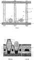
- FIG. 1 is a plane schematic view illustrating an array substrate according to one technique
- FIG.2 is a cross-sectional schematic view illustrating the liquid crystal display device, and the cross-sectional schematic view is cut along a line of A-A' in FIG. 1 . As shown in FIG. 1 and FIG.
- the array substrate includes a base substrate 01, and a buffer layer 02, an active layer 03, a gate insulation layer 04, a gate line layer (including a gate line 05 and a gate electrode G), an inter-layer insulation layer 06, a data line layer (including a data line 07, a source electrode S and a drain electrode D), a passivation layer 08 and a via hole 09 provided in the passivation layer 08, a pixel electrode 010, an inter-electrode insulation layer 011 and a common electrode 012, which are sequentially provided on the base substrate 01.
- the gate lines 05 and the data lines 07 intersect with each other to define a plurality of sub-pixels, and each sub-pixel includes a thin film transistor and the pixel electrode.
- the thin film transistor is formed by the active layer 03, the gate electrode G, the source electrode S and the drain electrode D, and the pixel electrode 010 is connected with the drain electrode D of the thin film transistor through the via hole 09.
- the opposed substrate includes another base substrate 016, and a black matrix 013, a passivation layer 014 and a spacer 015 which are sequentially provided on the base substrate 016.
- the spacer 015 is provided on the opposed substrate, and a top end thereof abuts on a flat region between adjacent sub-pixels of the array substrate.
- a size of the sub-pixel becomes smaller and smaller; in this case, since there is the via hole 09, an area of the flat region between adjacent sub-pixels of the array substrate is reduced; if the liquid crystal display device suffers an external force, the spacer 05 may easily slide into the via hole 09 and scratch an alignment layer (not shown) provided on a surface of the array substrate in the process of sliding.
- the spacer 05 slides into the via hole 09, it is hard to realize a uniform gap between the array substrate and the opposed substrate or maintain uniformity of the thickness of the liquid crystal layer, resulting in uneven displayed image, and decreasing display quality; and in the case that the alignment layer is scratched, abnormal alignment of the liquid crystal molecules in the liquid crystal layer is caused, resulting in light leakage.
- an array substrate comprises: a base substrate; a plurality of gate lines and a plurality of data lines formed on the base substrate, the plurality of gate lines and the plurality of data lines intersecting with each other to define a plurality of sub-pixels, each of the sub-pixels including a thin film transistor and a pixel electrode, and the plurality of sub-pixels including a first sub-pixel; a passivation layer formed on the base substrate and covering the gate lines, the data lines and the thin film transistors, a via hole being provided in the passivation layer and the pixel electrode being formed on the passivation layer and connected with a drain electrode or a source electrode of the thin film transistor through the via hole in each of the sub-pixels; and a first spacer, provided in the via hole of the first sub-pixel.
- the plurality of sub-pixels further include a second sub-pixel; and the array substrate further comprises a second spacer provided in the via hole of the second sub-pixel.
- a height of the first spacer is greater than a height of the second spacer on the base substrate.
- each of the sub-pixels further includes a common electrode and an inter-electrode insulation layer provided between the common electrode and the pixel electrode; the inter-electrode insulation layer has a portion provided on the first spacer but does not have a portion provided on the second spacer, and/or the common electrode has a portion provided on the first spacer but does not have a portion provided on the second spacer.
- a height of the first spacer is equal to a height of the second spacer on the base substrate; each of the sub-pixels further includes a common electrode and an inter-electrode insulation layer provided between the common electrode and the pixel electrode; the inter-electrode insulation layer has a portion provided on the first spacer but does not have a portion provided on the second spacer, and/or the common electrode has a portion provided on the first spacer but does not have a portion provided on the second spacer.
- the array substrate further comprises a third spacer provided above at least one of the gate lines and/or at least one of the data lines.
- the array substrate further comprises a shielding electrode provided on the third spacer.
- each of the sub-pixels further includes a common electrode and an inter-electrode insulation layer provided between the common electrode and the pixel electrode; and the shielding electrode is provided in a same layer with the common electrode.
- each of the sub-pixels further includes a common electrode and an inter-electrode insulation layer provided between the common electrode and the pixel electrode; the inter-electrode insulation layer has a portion provided on the first spacer and the common electrode has a portion provided on the first spacer; the third spacer is provided with a shielding electrode provided in a same layer with the common electrode.
- a display device comprises: an array substrate; an opposed substrate, provided opposite to the array substrate; and a liquid crystal layer, provided between the array substrate and the opposed substrate.
- the array substrate comprises: a base substrate; a plurality of gate lines and a plurality of data lines formed on the base substrate, the plurality of gate lines and the plurality of data lines intersecting with each other to define a plurality of sub-pixels, each of the sub-pixels including a thin film transistor and a pixel electrode, and the plurality of sub-pixels including a first sub-pixel; a passivation layer formed on the base substrate and covering the gate lines, the data lines and the thin film transistors, a via hole being provided in the passivation layer and the pixel electrode being formed on the passivation layer and connected with a drain electrode or a source electrode of the thin film transistor through the via hole in each of the sub-pixels; and a first spacer, provided in the via hole of the first sub-pixel.
- the plurality of sub-pixels further include a second sub-pixel
- the array substrate further comprises a second spacer provided in the via hole of the second sub-pixel.
- a height of the first spacer is greater than a height of the second spacer on the base substrate.
- each of the sub-pixels further includes a common electrode and an inter-electrode insulation layer provided between the common electrode and the pixel electrode; and the inter-electrode insulation layer has a portion provided on the first spacer but does not have a portion provided on the second spacer, and/or the common electrode has a portion provided on the first spacer but does not have a portion provided on the second spacer.
- a height of the first spacer is equal to a height of the second spacer on the base substrate; each of the sub-pixels further includes a common electrode and an inter-electrode insulation layer provided between the common electrode and the pixel electrode; the inter-electrode insulation layer has a portion provided on the first spacer but does not have a portion provided on the second spacer, and/or the common electrode has a portion provided on the first spacer but does not have a portion provided on the second spacer.
- the display device further comprises a third spacer provided above at least one of the gate lines and/or at least one of the data lines.
- the display device further comprises a shielding electrode provided on the third spacer.
- each of the sub-pixels further includes a common electrode and an inter-electrode insulation layer provided between the common electrode and the pixel electrode; and the shielding electrode is provided in a same layer with the common electrode.
- each of the sub-pixels further includes a common electrode and an inter-electrode insulation layer provided between the common electrode and the pixel electrode; the inter-electrode insulation layer has a portion provided on the first spacer and the common electrode has a portion provided on the first spacer; and the third spacer is provided with a shielding electrode provided in a same layer with the common electrode.
- the opposed substrate includes a color filter layer, and the color filter layer has a portion provided above the first spacer.
- a fabrication method of an array substrate comprises: forming a plurality of gate lines and a plurality of data lines on a base substrate, the plurality of gate lines and the plurality of data lines intersecting with each other to define a plurality of sub-pixels, each of the sub-pixels including a thin film transistor and a pixel electrode, and the plurality of sub-pixels including a first sub-pixel; forming a passivation layer covering the gate lines, the data lines and the thin film transistors on the base substrate, a via hole being provided in the passivation layer and the pixel electrode being formed on the passivation layer and connected with a drain electrode or a source electrode of the thin film transistor through the via hole in each of the sub-pixels; and forming a first spacer in the via hole of the first sub-pixel.
- FIG. 3 is a plane schematic view illustrating the array substrate according to the embodiments of the present disclosure
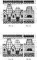
- FIG. 4a and FIG. 4b are cross-sectional schematic views cut along a line of A-A' in FIG. 3 .
- FIG. 3 and FIG. 4a are cross-sectional schematic views cut along a line of A-A' in FIG. 3 .
- the array substrate comprises: a base substrate 1; a plurality of gate lines 5 and a plurality of data lines 7 formed on the base substrate 1, the plurality of gate lines 5 and the plurality of data lines 7 intersecting with each other to define a plurality of sub-pixels, each sub-pixel including a thin film transistor and a pixel electrode 10, and the plurality of sub-pixels including a first sub-pixel; a passivation layer 8 formed on the base substrate 1 and covering the gate lines 5, the data lines 7 and the thin film transistors, a via hole 9 being provided in the passivation layer and the pixel electrode 10 being formed on the passivation layer 8 and connected with a drain electrode D or a source electrode S of the thin film transistor through the via hole 9 in each sub-pixel; and a first spacer 15, provided in the via hole of the first sub-pixel.
- an end of the first spacer abuts on the opposed substrate, so that the first spacer is configured for maintaining a uniform gap between the array substrate and the opposed substrate and maintaining uniformity of a thickness of a liquid crystal layer sandwiched between the array substrate and the opposed substrate.
- the first spacer is provided in the via hole of the first sub-pixel. Therefore, even if the display device suffers an external force, the first spacer does not easily slide, and thus situations of nonuniform thickness of the liquid crystal layer and scratches of an alignment layer (not shown in the drawings, the alignment layer is provided on a surface of the array substrate facing the opposed substrate) caused by the first spacer sliding into the via hole are avoided. And thus, the uniform gap between the array substrate and the opposed substrate and the uniformity of the thickness of the liquid crystal layer are maintained well, and light leakage caused by scratches of the alignment layer is avoided, and the display quality is improved.
- the thin film transistor includes an active layer 03, a gate electrode G, a source electrode S and a drain electrode D; the gate electrode G is connected with the gate line 5 or integrally formed with the gate line 5, the source electrode S or the drain electrode D is connected with the data line 7 or integrally formed with the data line 7, and the drain electrode D or the source electrode S is connected with the pixel electrode 10.
- a buffer layer 2 is formed on the base substrate 1 at first, so as to prevent impurities in the base substrate 1 from entering the active layer 3 and improve the quality of the active layer 3; and the active layer 3, a gate insulation layer 4, a gate line layer (including the gate line 5 and the gate electrode G), an inter-layer insulation layer 6, and a data line layer (including the data line 7, the source electrode S and the drain electrode D) are sequentially formed on the buffer layer 2.
- the embodiments of the present disclosure are not limited thereto, the array substrate according to the embodiments of the present disclosure may not adopt the buffer layer, and these layers such as the active layer 3, the gate insulation layer 4, the gate line layer (including the gate line 5 and the gate electrode G), the inter-layer insulation layer 6, and the data line layer (including the data line 7, the source electrode S and the drain electrode D) may be provided in any known stacking sequence. Accordingly, in the array substrate according to the embodiments of the present disclosure, the thin film transistor is of a bottom gate type, a top gate type or any known type.
- the plurality of sub-pixels further include a second sub-pixel, and the second sub-pixel is different from the first sub-pixel described above;
- the array substrate according to the embodiments of the present disclosure further comprises a second spacer 16, and the second spacer 16 is provided in the via hole 9 of the second sub-pixel.
- a height of the first spacer 15 is greater than a height of the second spacer 16 on the base substrate 1; in this case, the first spacer 15 is regarded as a main spacer, and the second spacer 16 is regarded as an assistant spacer.
- the liquid crystal layer contracts at a low temperature so that a volume thereof is reduced. If too many spacers are provided, the opposed substrate is not deformed, and at the low temperature, bubbles are generated in the liquid crystal layer if the display device is suddenly impacted by an external force, resulting in a defect of low temperature bubble.
- the first spacer 15 and the second spacer 16 are provided, and the height of the first spacer 15 is greater than the height of the second spacer 16, so that not only the defect of low temperature bubble is avoided, but also the defect of pressing is avoided.
- the second spacer 16 is provided in the via hole 9 of the second sub-pixel, the second spacer 16 is prevented from sliding to scratch the alignment layer, and thus abnormal alignment of liquid crystal molecules in the liquid crystal layer and light leakage caused by scratches of the alignment layer are avoided.
- the first spacer 15 and the second spacer 16 are formed by two different patterning processes with using two different single-tone masks.
- the first spacer 15 and the second spacer 16 for example are formed by a single patterning process with using one dual-tone mask.
- each sub-pixel further includes a common electrode 12 and an inter-electrode insulation layer 11 provided between the common electrode 12 and the pixel electrode 10.
- the inter-electrode insulation layer 11 has a portion provided on the first spacer 15 but does not have a portion provided on the second spacer 15; and/or, the common electrode 12 has a portion provided on the first spacer 15 but does not have a portion provided on the second spacer 16.
- the first spacer 15 and the second spacer 16 for example are formed by the single patterning process with using one dual-tone mask; in order to effectively avoid the defect of low temperature bubble and the defect of pressing, it is necessary to form an enough height difference between the first spacer 15 and the second spacer 16, which increases technical difficulty in the patterning process of using the dual-tone mask.
- the inter-electrode insulation layer 11 has the portion provided on the first spacer 15 but does not have the portion provided on the second spacer 16 and/or the common electrode 12 has the portion provided on the first spacer 15 but does not have the portion provided on the second spacer 16
- technical requirements on the patterning process of using the dual-tone mask is reduced and flexibility in designs of the first spacer 15 and the second spacer 16 is increased while the defect of low temperature bubble and the defect of pressing are avoided effectively.
- the first spacer 15 and the portion of the inter-electrode insulation layer 11 and/or the portion of the common electrode 12 provided on the spacer 15 are regarded as the main spacer.
- the portion of the inter-electrode insulation layer 11 provided on the first spacer 15 may be disconnected from or connected with other portions of the inter-electrode insulation layer 11, and the portion of the common electrode 12 provided on the first spacer 15 may be disconnected from or connected with other portions of the common electrode 12.
- both the portion of the inter-electrode insulation layer 11 and the portion of the common electrode 12 are formed on the first spacer 15; for example, in the case that the height of the first spacer 15 is greater than the height of the second spacer 16, neither the portion of the inter-electrode insulation layer 11 or the portion of the common electrode 12 is formed on the first spacer 15, or only one of the portion of the inter-electrode insulation layer 11 and the portion of the common electrode 12 is formed on the first spacer 15.
- FIG. 5a and FIG. 5b are cross-sectional schematic views illustrating the array substrate according to the embodiments of the present disclosure, which are cut along the line of A-A' in FIG. 3 .
- the height of the first spacer 15 is equal to the height of the second spacer 16 on the base substrate 1. Since the height of the first spacer 15 is equal to the height of the second spacer 16, the first spacer 15 and the second spacer 16 are formed by a single patterning process with using one single-tone mask, which reduces the technical difficulty and technical cost. Further, for example, as shown in FIG. 5a and FIG.
- the inter-electrode insulation layer 11 has the portion provided on the first spacer 15 but does not have the portion provided on the second spacer 16 and/or the common electrode 12 has the portion provided on the first spacer 15 but does not have the portion provided on the second spacer 16, in this way, the defect of low temperature bubble and the defect of pressing are avoided as well.
- the first spacer 15 and the portion of the inter-electrode insulation layer 11 and/or the portion of the common electrode 12 provided on the first spacer 15 are regarded as the main spacer.
- the portion of the inter-electrode insulation layer 11 provided on the first spacer 15 is disconnected from or connected with other portions of the inter-electrode insulation layer 11, and the portion of the common electrode 12 provided on the first spacer 15 is disconnected from or connected with other portions of the common electrode 12.
- both the portion of the inter-electrode insulation layer 11 and the portion of the common electrode 12 are formed on the first spacer 15; for example, in a case that the height of the first spacer 15 is equal to the height of the second spacer 16, only one of the portion of the inter-electrode insulation layer 11 and the portion of the common electrode 12 is formed on the first spacer 15.
- neither the first spacer 15 nor the second spacer 16 is provided in the via hole(s) of one or some sub-pixels.
- a ratio of a number of the first spacer 15 to a number of the second spacer 16 is 1:10 to 1:100, and further, for example, is 1:18 or 1:36.
- FIG. 6 is a plane schematic view II of the array substrate according to the embodiments of the present disclosure
- FIG. 7a and FIG. 7b are cross-sectional schematic views cut along a line of A-A' in FIG. 6
- the array substrate according to the embodiments of the present disclosure further comprises a third spacer 17 provided above at least one of the data line 7 and/or at least one of the gate line 5. Since the third spacer 17 has a certain height, it blocks electric line between adjacent sub-pixels, and thus electric field interference between adjacent sub-pixels is reduced.
- the array substrate according to the embodiments of the present disclosure comprises a display region for arranging the plurality of sub-pixels and a peripheral region surrounding the display region.
- a length of the third spacer 17 is less than or equal to a length of the display region along an extending direction of the third spacer 17, that is, the third spacer 17 is provided inside the display region.
- the array substrate according to the embodiments of the present disclosure further comprises a shielding electrode 18 provided on the third spacer 17, so as to further reduce electric field interference between adjacent sub-pixels.
- a voltage is applied to the shielding electrode 18; for example, a low level voltage (such as a 0-level voltage) is applied to the shielding electrode 18.
- the shielding electrode 18 is provided in a same layer with the common electrode 12, so that the shielding electrode 18 and the common electrode 12 are formed by a single patterning process at the same time, to simplify the fabrication process.
- the shielding electrode 18 is connected with the common electrode 12, so that a common voltage is applied to the shielding electrode 18.
- the shielding electrode 18 is disconnected from the common electrode 12, so that the shielding electrode 18 and the common electrode 12 are driven separately.
- a portion of the inter-electrode insulation layer 11 is further provided between the shielding electrode 18 and the third spacer 17.
- the portion of the inter-electrode insulation layer 11 provided between the shielding electrode 18 and the third spacer 17 is disconnected from or connected with other portions of the inter-electrode insulation layer 11.
- the shielding electrode 18 covers an upper surface and a side surface of the third spacer 17.
- the first spacer 15, the second spacer 16 and the third spacer 17 are fabricated to have a same height, as shown in FIGS. 8a and 8b ; in this case, the first spacer 15, the second spacer 16 and the third spacer 17 are formed by a single patterning process with using one single-tone mask.
- the inter-electrode insulation layer 11 has the portion provided on the first spacer 15 and the common electrode 12 has the portion provided on the first spacer 15, and the shielding electrode 18 provided in the same layer with the common electrode 12 is formed on the third spacer 17; and therefore, the first spacer 15 and the portion of the inter-electrode insulation layer 11 and the portion of the common electrode 12 provided on the first spacer 15 are regarded as the main spacer, the third spacer 17 and the shielding electrode 18 provided on the third spacer 17 are regarded as a first assistant spacer, the second spacer 16 is regarded as a second assistant spacer, and a height of the main spacer, a height of the first assistant spacer and a height of the second assistant spacer are sequentially reduced, so that the defect of low temperature bubble and the defect of pressing are more effectively avoided.
- the base substrate 1, the buffer layer 2, the active layer 3, the gate insulation layer 4, the gate line layer (including the gate line 5 and the gate electrode G), the inter-layer insulation layer 6, the data line layer (including the data line 7, the source electrode S and the drain electrode D), the passivation layer 8, the pixel electrode 10, the inter-electrode insulation layer 11 and the common electrode 12 may be made of any known material or formed by any known method, which will not be repeated here.
- the active layer 3 is made of a low temperature polysilicon.
- the passivation layer 8 is made of an organic resin, for example, an acrylic resin.
- the spacer (such as the first spacer 15, the second spacer 16 and the third spacer 17) is made of an organic resin, for example, a negative PR adhesive.
- the first spacer 15, the second spacer 16 and the third spacer 17 are made of a same material or different materials.
- first spacer 15 and the second spacer 16 formed in the via hole 9 are in direct contact with the pixel electrode 10 formed in the via hole 9; however, the embodiments of the present disclosure are not limited thereto, an inserting layer may be formed between the first spacer 15 and the pixel electrode 10 and/or between the second spacer 16 and the pixel electrode 10 according to actual needs.
- a display device comprises: the array substrate described above; an opposed substrate, provided opposite to the array substrate, wherein an end of the first spacer abuts on the opposed substrate; and a liquid crystal layer, provided between the array substrate and the opposed substrate. Since the display device according to the embodiments of the present disclosure comprises the array substrate described above, even if the display device is under action of an external force, the first spacer is not easily slide, and thus situations of nonuniform thickness of the liquid crystal layer and scratches of the alignment layer (not shown, which is provided on a surface of the array substrate facing the opposed substrate) caused by the first spacer sliding into the via hole are avoided. And thus, the uniform gap between the array substrate and the opposed substrate is realized, the uniformity in the thickness of the liquid crystal layer is maintained well, the light leakage caused by scratches of the alignment layer is avoided, and the display quality is improved.
- FIGS. 9a and 9b, FIGS. 10a and 10b , FIGS. 11a and 11b, FIGS. 12a and 12b , and FIGS. 13a and 13b are cross-sectional schematic views illustrating the display device according to the embodiments of the present disclosure.
- the opposed substrate includes a base substrate 20, and a black matrix 13 and a passivation layer 14 which are sequentially provided on the base substrate 20; the first spacer 15, the second spacer 16 and the third spacer 17 as described above are all provided in a region covered by the black matrix 13.
- the display device shown in FIGS. 9a and 9b adopts the array substrate shown in FIGS. 4a and 4b
- the display device shown in FIGS. 10a and 10b adopts the array substrate shown in FIGS. 5a and 5b
- the display device shown in FIGS. 11a and 11b adopts the array substrate shown in FIGS. 7a and 7b
- the display device shown in FIGS. 12a and 12b adopts the array substrate shown in FIGS. 8a and 8b , which will not be repeated here.
- the display device shown in FIGS. 13a and 13b is almost same as the display device shown in FIGS. 9a and 9b .
- the opposed substrate further includes a color filter layer 19.
- the color filter layer 19 has a portion provided above the first spacer 15 but does not have a portion provided above the second spacer 16, which is also conducive to avoiding the defect of low temperature bubble and the defect of pressing and further reduce technical requirements on a patterning process of using the dual-tone mask and increase flexibility in designs of the first spacer 15 and the second spacer 16.
- the opposed substrate shown in FIGS. 13a and 13b may replace the opposed substrate shown in FIGS. 10a and 10b , FIGS. 11a and 11b, and FIGS. 12a and 12b .
- the display device is any product or component having a display function, such as a liquid crystal display panel, a liquid crystal display device, a mobile phone, a tablet PC, a TV, a monitor, a laptop computer, a digital photo frame, a navigator, etc.
- a display function such as a liquid crystal display panel, a liquid crystal display device, a mobile phone, a tablet PC, a TV, a monitor, a laptop computer, a digital photo frame, a navigator, etc.
- the fabrication method of the array substrate comprises: forming a plurality of gate lines 5 and a plurality of data lines 7 on a base substrate 1, the plurality of gate lines 5 and the plurality of data lines 7 intersecting with each other to define a plurality of sub-pixels, each sub-pixel including a thin film transistor and a pixel electrode 10, and the plurality of sub-pixels including a first sub-pixel; forming a passivation layer 8 covering the gate lines 5, the data lines 7 and the thin film transistors on the base substrate 1, a via hole being provided in the passivation layer 8 and the pixel electrode 10 being formed on the passivation layer 8 and connected with a drain electrode D or a source electrode S of the thin film transistor through the via hole 9 in the each sub-pixel; and forming a first spacer 15 in the via hole of the first sub-pixel 9.
- the first spacer is formed in the via hole of the first sub-pixel. And thus, even if a display device formed by bonding the array substrate and an opposed substrate is under action of external forces, the first spacer is not easily slide, so that situations of nonuniform thickness of the liquid crystal layer and scratches of an alignment layer (not shown, which is provided on a surface of the array substrate facing the opposed substrate) caused by the first spacer sliding into the via hole are avoided. And thus, a uniform gap between the array substrate and the opposed substrate and uniformity of a thickness of the liquid crystal layer are maintained well, and a light leakage caused by scratches of the alignment layer is avoided, and a display quality is improved.
- the plurality of sub-pixels further include a second sub-pixel
- the fabrication method of the array substrate further comprises: forming a second spacer 16 in the via hole 9 of the second sub-pixel.
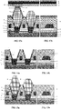
- FIGS. 14a and 14b to FIGS. 16a and 16b show a flow schematic view I of the fabrication method of the array substrate according to the embodiments of the present disclosure.
- a buffer layer 2 is formed on a base substrate 1, and an active layer 3, a gate insulation layer 4, a gate line layer (including the gate line 5 and a gate electrode G), an inter-layer insulation layer 6, a data line layer (including the data line 7, the source electrode S and the drain electrode D), the passivation layer 8 and the via hole 9, and the pixel electrode 10 are sequentially formed on the buffer layer.
- the thin film transistor is formed by the active layer 3, the gate electrode G, the source electrode S and the drain electrode D, and the pixel electrode 10 is connected with the drain electrode D or the source electrode S of the thin film transistor through the via hole 9 provided in the passivation layer 8.
- the respective layers described above may be made of any known materials or formed by any known methods, which will not be repeated here.
- the sequence for stacking the respective layers described above is not limited to the sequence shown in FIGS. 14a and 14b , and may be adjusted according to actual needs, which will not be repeated here.
- a material layer for forming the spacer (for example, such material layer for forming the spacer is formed by a photoresist adhesive and has a thickness of 4 to 6 ⁇ m) is formed, and the material layer for forming the spacer is patterned by using a dual-tone mask (such as, a half-tone mask and a gray-tone mask), to form the first spacer 15 and the second spacer 16 by a single patterning process at the same time, and a height of the first spacer 15 is greater than a height of the second spacer 16, as shown in FIGS. 15a and 15b .
- a dual-tone mask such as, a half-tone mask and a gray-tone mask
- the fabrication method of the array substrate further comprises: forming an inter-electrode insulation layer 11 on the pixel electrode 10, and the inter-electrode insulation layer 11 has a portion provided on the first spacer 15 but does not have a portion provided on the second spacer 16, as shown in FIGS. 16a and 16b .
- the fabrication method of the array substrate further comprises: forming a common electrode 12 on the inter-electrode insulation layer 11, and the common electrode 12 has a portion provided on the first spacer 15 but does not have a portion provided on the second spacer 16, and thus the array substrate shown in FIGS. 4a and 4b is obtained.
- FIGS. 17a and 17b to FIGS. 18a and 18b show a flow schematic view II of the fabrication method of the array substrate according to the embodiments of the present disclosure.
- the material layer for forming the spacer (for example, the material layer for forming the spacer is formed by the photoresist adhesive and has a thickness of 4 to 6 ⁇ m) is formed, and the material layer for forming the spacer is patterned by using a single-tone mask, to form the first spacer 15 and the second spacer 16 by a single patterning process at the same time, and the height of the first spacer 15 is equal to the height of the second spacer 16, as shown in FIGS. 17a and 17b .
- the fabrication method of the array substrate further comprises: forming the inter-electrode insulation layer 11 on the pixel electrode 10, and the inter-electrode insulation layer 11 has the portion provided on the first spacer 15 but does not have the portion provided on the second spacer 16, as shown in FIGS. 18a and 18b .
- the fabrication method of the array substrate further comprises: forming the common electrode 12 on the inter-electrode insulation layer 11, and the common electrode 12 has the portion provided on the first spacer 15 but does not have the portion provided on the second spacer 16, and thus the array substrate shown in FIGS. 5a and 5b is obtained.
- FIG. 19a and FIG. 19b to FIG. 20a and FIG. 20b show a flow schematic view III of the fabrication method of the array substrate according to the embodiments of the present disclosure.
- the first spacer 15, the second spacer 16 and a third spacer 17 are formed, as shown in FIGS. 19a and 19b .
- the first spacer 15, the second spacer 16 and the third spacer 17 are formed by three different patterning processes by using three different masks.
- the first spacer 15 and the second spacer 16 are formed by a single patterning process with using one dual-tone mask, and then the third spacer 17 is formed by a single patterning process with using one single-tone mask.
- the first spacer 15, the second spacer 16 and the third spacer 17 are fabricated to have a same height; in this way, the first spacer 15, the second spacer 16 and the third spacer 17 are formed by a single patterning process with using one single-tone mask.
- the fabrication method of the array substrate further comprises: forming the inter-electrode insulation layer 11 on the pixel electrode 10, and the inter-electrode insulation layer 11 has the portion provided on the first spacer 15 but does not have the portion provided on the second spacer 16, as shown in FIGS. 20a and 20b .
- the fabrication method of the array substrate further comprises: forming the common electrode 12 on the inter-electrode insulation layer 11, and the common electrode 12 has the portion provided on the first spacer 15 but does not have the portion provided on the second spacer 16. Further, the fabrication method of the array substrate further comprises: forming a shielding electrode 18 on the third spacer 17, and thus the array substrate shown in FIGS. 7a and 7b is obtained.
- the common electrode 12 and the shielding electrode 18 are formed by patterning a common electrode material layer at the same time.
Landscapes
- Physics & Mathematics (AREA)
- Nonlinear Science (AREA)
- Mathematical Physics (AREA)
- Chemical & Material Sciences (AREA)
- Crystallography & Structural Chemistry (AREA)
- General Physics & Mathematics (AREA)
- Optics & Photonics (AREA)
- Engineering & Computer Science (AREA)
- Microelectronics & Electronic Packaging (AREA)
- Liquid Crystal (AREA)
- Geometry (AREA)
- Devices For Indicating Variable Information By Combining Individual Elements (AREA)
Abstract
Description
- Embodiments of the present disclosure relate to an array substrate, a fabrication method of the array substrate, and a display device comprising the array substrate.
- At present, a liquid crystal display device plays a dominant role in a flat-plate display device market. The liquid crystal display device mainly includes an array substrate and an opposed substrate which are provided opposite to each other, and a liquid crystal layer sandwiched between the array substrate and the opposed substrate. In order to control a uniform gap between the array substrate and the opposed substrate and maintain uniformity of thickness of the liquid crystal layer, a spacer is further provided between the array substrate and the opposed substrate.
-
FIG. 1 is a plane schematic view illustrating an array substrate according to one technique;FIG.2 is a cross-sectional schematic view illustrating the liquid crystal display device, and the cross-sectional schematic view is cut along a line of A-A' inFIG. 1 . As shown inFIG. 1 and FIG. 2 , the array substrate includes abase substrate 01, and abuffer layer 02, anactive layer 03, agate insulation layer 04, a gate line layer (including agate line 05 and a gate electrode G), aninter-layer insulation layer 06, a data line layer (including adata line 07, a source electrode S and a drain electrode D), apassivation layer 08 and avia hole 09 provided in thepassivation layer 08, apixel electrode 010, aninter-electrode insulation layer 011 and acommon electrode 012, which are sequentially provided on thebase substrate 01. Thegate lines 05 and thedata lines 07 intersect with each other to define a plurality of sub-pixels, and each sub-pixel includes a thin film transistor and the pixel electrode. In each sub-pixel, the thin film transistor is formed by theactive layer 03, the gate electrode G, the source electrode S and the drain electrode D, and thepixel electrode 010 is connected with the drain electrode D of the thin film transistor through thevia hole 09. The opposed substrate includes anotherbase substrate 016, and ablack matrix 013, apassivation layer 014 and aspacer 015 which are sequentially provided on thebase substrate 016. - With further reference to
FIG. 1 and FIG. 2 , thespacer 015 is provided on the opposed substrate, and a top end thereof abuts on a flat region between adjacent sub-pixels of the array substrate. As a resolution of the liquid crystal display device increases, a size of the sub-pixel becomes smaller and smaller; in this case, since there is thevia hole 09, an area of the flat region between adjacent sub-pixels of the array substrate is reduced; if the liquid crystal display device suffers an external force, thespacer 05 may easily slide into thevia hole 09 and scratch an alignment layer (not shown) provided on a surface of the array substrate in the process of sliding. In the case that thespacer 05 slides into thevia hole 09, it is hard to realize a uniform gap between the array substrate and the opposed substrate or maintain uniformity of the thickness of the liquid crystal layer, resulting in uneven displayed image, and decreasing display quality; and in the case that the alignment layer is scratched, abnormal alignment of the liquid crystal molecules in the liquid crystal layer is caused, resulting in light leakage. - According to embodiments of the disclosure, an array substrate is provided. The array substrate comprises: a base substrate; a plurality of gate lines and a plurality of data lines formed on the base substrate, the plurality of gate lines and the plurality of data lines intersecting with each other to define a plurality of sub-pixels, each of the sub-pixels including a thin film transistor and a pixel electrode, and the plurality of sub-pixels including a first sub-pixel; a passivation layer formed on the base substrate and covering the gate lines, the data lines and the thin film transistors, a via hole being provided in the passivation layer and the pixel electrode being formed on the passivation layer and connected with a drain electrode or a source electrode of the thin film transistor through the via hole in each of the sub-pixels; and a first spacer, provided in the via hole of the first sub-pixel.
- For example, the plurality of sub-pixels further include a second sub-pixel; and the array substrate further comprises a second spacer provided in the via hole of the second sub-pixel.
- For example, a height of the first spacer is greater than a height of the second spacer on the base substrate.
- For example, each of the sub-pixels further includes a common electrode and an inter-electrode insulation layer provided between the common electrode and the pixel electrode; the inter-electrode insulation layer has a portion provided on the first spacer but does not have a portion provided on the second spacer, and/or the common electrode has a portion provided on the first spacer but does not have a portion provided on the second spacer.
- For example, a height of the first spacer is equal to a height of the second spacer on the base substrate; each of the sub-pixels further includes a common electrode and an inter-electrode insulation layer provided between the common electrode and the pixel electrode; the inter-electrode insulation layer has a portion provided on the first spacer but does not have a portion provided on the second spacer, and/or the common electrode has a portion provided on the first spacer but does not have a portion provided on the second spacer.
- For example, the array substrate further comprises a third spacer provided above at least one of the gate lines and/or at least one of the data lines.
- For example, the array substrate further comprises a shielding electrode provided on the third spacer.
- For example, each of the sub-pixels further includes a common electrode and an inter-electrode insulation layer provided between the common electrode and the pixel electrode; and the shielding electrode is provided in a same layer with the common electrode.
- For example, a height of the first spacer, a height of the second spacer and a height of the third spacer are equal to each other on the base substrate; each of the sub-pixels further includes a common electrode and an inter-electrode insulation layer provided between the common electrode and the pixel electrode; the inter-electrode insulation layer has a portion provided on the first spacer and the common electrode has a portion provided on the first spacer; the third spacer is provided with a shielding electrode provided in a same layer with the common electrode.
- According to the embodiments of the disclosure, a display device is provided. The display device comprises: an array substrate; an opposed substrate, provided opposite to the array substrate; and a liquid crystal layer, provided between the array substrate and the opposed substrate. The array substrate comprises: a base substrate; a plurality of gate lines and a plurality of data lines formed on the base substrate, the plurality of gate lines and the plurality of data lines intersecting with each other to define a plurality of sub-pixels, each of the sub-pixels including a thin film transistor and a pixel electrode, and the plurality of sub-pixels including a first sub-pixel; a passivation layer formed on the base substrate and covering the gate lines, the data lines and the thin film transistors, a via hole being provided in the passivation layer and the pixel electrode being formed on the passivation layer and connected with a drain electrode or a source electrode of the thin film transistor through the via hole in each of the sub-pixels; and a first spacer, provided in the via hole of the first sub-pixel. An end of the first spacer abuts on the opposed substrate.
- For example, the plurality of sub-pixels further include a second sub-pixel, and the array substrate further comprises a second spacer provided in the via hole of the second sub-pixel.
- For example, a height of the first spacer is greater than a height of the second spacer on the base substrate.
- For example, each of the sub-pixels further includes a common electrode and an inter-electrode insulation layer provided between the common electrode and the pixel electrode; and the inter-electrode insulation layer has a portion provided on the first spacer but does not have a portion provided on the second spacer, and/or the common electrode has a portion provided on the first spacer but does not have a portion provided on the second spacer.
- For example, a height of the first spacer is equal to a height of the second spacer on the base substrate; each of the sub-pixels further includes a common electrode and an inter-electrode insulation layer provided between the common electrode and the pixel electrode; the inter-electrode insulation layer has a portion provided on the first spacer but does not have a portion provided on the second spacer, and/or the common electrode has a portion provided on the first spacer but does not have a portion provided on the second spacer.
- For example, the display device further comprises a third spacer provided above at least one of the gate lines and/or at least one of the data lines.
- For example, the display device further comprises a shielding electrode provided on the third spacer.
- For example, each of the sub-pixels further includes a common electrode and an inter-electrode insulation layer provided between the common electrode and the pixel electrode; and the shielding electrode is provided in a same layer with the common electrode.
- For example, a height of the first spacer, a height of the second spacer and a height of the third spacer are equal to each other on the base substrate; each of the sub-pixels further includes a common electrode and an inter-electrode insulation layer provided between the common electrode and the pixel electrode; the inter-electrode insulation layer has a portion provided on the first spacer and the common electrode has a portion provided on the first spacer; and the third spacer is provided with a shielding electrode provided in a same layer with the common electrode.
- For example, the opposed substrate includes a color filter layer, and the color filter layer has a portion provided above the first spacer.
- According to the embodiments of the disclosure, a fabrication method of an array substrate is provided. The method comprises: forming a plurality of gate lines and a plurality of data lines on a base substrate, the plurality of gate lines and the plurality of data lines intersecting with each other to define a plurality of sub-pixels, each of the sub-pixels including a thin film transistor and a pixel electrode, and the plurality of sub-pixels including a first sub-pixel; forming a passivation layer covering the gate lines, the data lines and the thin film transistors on the base substrate, a via hole being provided in the passivation layer and the pixel electrode being formed on the passivation layer and connected with a drain electrode or a source electrode of the thin film transistor through the via hole in each of the sub-pixels; and forming a first spacer in the via hole of the first sub-pixel.
- In order to clearly illustrate the technical solution of the embodiments of the present disclosure, the drawings of the embodiments will be briefly described in the following; it is obvious that the described drawings are only related to some embodiments of the present disclosure and thus are not limitative of the present disclosure.
-
FIG. 1 is a plane schematic view illustrating an array substrate according to one technique; -
FIG. 2a and FIG. 2b are cross-sectional schematic views illustrating a liquid crystal display device ofFIG. 1 , which are cut along a line of A-A' inFIG. 1 ; -
FIG. 3 is a plane schematic view I illustrating an array substrate according to embodiments of the present disclosure; -
FIG. 4a and FIG. 4b are cross-sectional schematic views illustrating the array substrate according to the embodiments of the present disclosure, which are cut along a line of A-A' inFIG. 3 , wherein a height of a first spacer is greater than a height of a second spacer on a base substrate; -
FIG. 5a and FIG. 5b are cross-sectional schematic views illustrating the array substrate according to the embodiments of the present disclosure, which are cut along the line of A-A' inFIG. 3 , wherein the height of the first spacer is equal to the height of the second spacer on the base substrate; -
FIG. 6 is a plane schematic view II illustrating another array substrate according to the embodiments of the present disclosure; -
FIG. 7a and FIG. 7b are cross-sectional schematic views illustrating the array substrate according to the embodiments of the present disclosure, which are cut along a line of A-A' inFIG. 6 , wherein a third spacer is formed; -
FIG. 8a and FIG. 8b are cross-sectional schematic views illustrating the array substrate according to the embodiments of the present disclosure, which are cut along the line of A-A' inFIG. 6 , wherein a height of the first spacer, a height of the second spacer and a height of the third spacer are same on the base substrate; -
FIG. 9a and FIG. 9b illustrate a cross-sectional schematic view I of a display device according to the embodiments of the present disclosure; -
FIG. 10a and FIG. 10b illustrate a cross-sectional schematic view II of the display device according to the embodiments of the present disclosure; -
FIG. 11a and FIG. 11b illustrate a cross-sectional schematic view III of the display device according to the embodiments of the present disclosure; -
FIG. 12a and FIG. 12b illustrate a cross-sectional schematic view IV of the display device according to the embodiments of the present disclosure; -
FIG. 13a and FIG. 13b illustrate a cross-sectional schematic view V of the display device according to the embodiments of the present disclosure; -
FIG. 14a and FIG. 14b toFIG. 16a and FIG. 16b illustrate a flow schematic view I of a fabrication method of an array substrate according to the embodiments of the present disclosure; -
FIG. 17a and FIG. 17b to FIG. 18a and FIG. 18b illustrate a flow schematic view II of the fabrication method of the array substrate according to the embodiments of the present disclosure; and -
FIG. 19a and FIG. 19b to FIG. 20a and FIG. 20b illustrate a flow schematic view III of the fabrication method of the array substrate according to the embodiments of the present disclosure. - In order to make objects, technical details and advantages of the embodiments of the present disclosure apparent, the technical solutions of the embodiment will be described in a clearly and fully understandable way in connection with the drawings related to the embodiments of the present disclosure. It is obvious that the described embodiments are just a part but not all of the embodiments of the present disclosure. Based on the described embodiments herein, those skilled in the art can obtain other embodiment(s), without any inventive work, which should be within the scope of the present disclosure.
- Unless otherwise specified, the technical terms or scientific terms here should be of general meanings as understood by those ordinarily skilled in the art. In the specification and claims of the present disclosure of the patent application, words such as "first", "second" and the like do not denote any order, quantity, or importance, but rather are used for distinguishing different components. Similarly, words such as "one", "a/an" or "the" or the like do not denote quantitative limitation, but rather indicate there is at least one. Wordings of "include" or "comprise" and the like denote that elements or objects appearing before the word of "include" or "comprise" cover the elements or the objects enumerated after the word of "include" or "comprise" or equivalents thereof, not exclusive of other elements or objects. Words such as "up", "down", "left", "right" and the like are only used for expressing relative positional relationship, in the case that the absolute position of a described object is changed, the relative positional relationship may also be correspondingly changed.
- According to embodiments of the disclosure, there is provided an array substrate.
FIG. 3 is a plane schematic view illustrating the array substrate according to the embodiments of the present disclosure;FIG. 4a and FIG. 4b are cross-sectional schematic views cut along a line of A-A' inFIG. 3 . In conjunction withFIG. 3 and FIG. 4a as well asFIG. 4b , the array substrate according to the embodiments of the present disclosure comprises: abase substrate 1; a plurality ofgate lines 5 and a plurality ofdata lines 7 formed on thebase substrate 1, the plurality ofgate lines 5 and the plurality ofdata lines 7 intersecting with each other to define a plurality of sub-pixels, each sub-pixel including a thin film transistor and apixel electrode 10, and the plurality of sub-pixels including a first sub-pixel; apassivation layer 8 formed on thebase substrate 1 and covering thegate lines 5, thedata lines 7 and the thin film transistors, a viahole 9 being provided in the passivation layer and thepixel electrode 10 being formed on thepassivation layer 8 and connected with a drain electrode D or a source electrode S of the thin film transistor through the viahole 9 in each sub-pixel; and afirst spacer 15, provided in the via hole of the first sub-pixel. - After the array substrate according to the embodiments of the present disclosure and an opposed substrate are bonded to form a display device, an end of the first spacer abuts on the opposed substrate, so that the first spacer is configured for maintaining a uniform gap between the array substrate and the opposed substrate and maintaining uniformity of a thickness of a liquid crystal layer sandwiched between the array substrate and the opposed substrate.
- In the array substrate according to the embodiments of the present disclosure, the first spacer is provided in the via hole of the first sub-pixel. Therefore, even if the display device suffers an external force, the first spacer does not easily slide, and thus situations of nonuniform thickness of the liquid crystal layer and scratches of an alignment layer (not shown in the drawings, the alignment layer is provided on a surface of the array substrate facing the opposed substrate) caused by the first spacer sliding into the via hole are avoided. And thus, the uniform gap between the array substrate and the opposed substrate and the uniformity of the thickness of the liquid crystal layer are maintained well, and light leakage caused by scratches of the alignment layer is avoided, and the display quality is improved.
- For example, the thin film transistor includes an
active layer 03, a gate electrode G, a source electrode S and a drain electrode D; the gate electrode G is connected with thegate line 5 or integrally formed with thegate line 5, the source electrode S or the drain electrode D is connected with thedata line 7 or integrally formed with thedata line 7, and the drain electrode D or the source electrode S is connected with thepixel electrode 10. - For example, as shown in
FIGS. 4a and 4b , in the array substrate according to the embodiments of the present disclosure, abuffer layer 2 is formed on thebase substrate 1 at first, so as to prevent impurities in thebase substrate 1 from entering theactive layer 3 and improve the quality of theactive layer 3; and theactive layer 3, agate insulation layer 4, a gate line layer (including thegate line 5 and the gate electrode G), aninter-layer insulation layer 6, and a data line layer (including thedata line 7, the source electrode S and the drain electrode D) are sequentially formed on thebuffer layer 2. However, the embodiments of the present disclosure are not limited thereto, the array substrate according to the embodiments of the present disclosure may not adopt the buffer layer, and these layers such as theactive layer 3, thegate insulation layer 4, the gate line layer (including thegate line 5 and the gate electrode G), theinter-layer insulation layer 6, and the data line layer (including thedata line 7, the source electrode S and the drain electrode D) may be provided in any known stacking sequence. Accordingly, in the array substrate according to the embodiments of the present disclosure, the thin film transistor is of a bottom gate type, a top gate type or any known type. - For example, with further reference to
FIG. 3 and FIG. 4a as well asFIG. 4b , the plurality of sub-pixels further include a second sub-pixel, and the second sub-pixel is different from the first sub-pixel described above; the array substrate according to the embodiments of the present disclosure further comprises asecond spacer 16, and thesecond spacer 16 is provided in the viahole 9 of the second sub-pixel. - For example, as shown in
FIGS. 4a and 4b , a height of thefirst spacer 15 is greater than a height of thesecond spacer 16 on thebase substrate 1; in this case, thefirst spacer 15 is regarded as a main spacer, and thesecond spacer 16 is regarded as an assistant spacer. Generally, the liquid crystal layer contracts at a low temperature so that a volume thereof is reduced. If too many spacers are provided, the opposed substrate is not deformed, and at the low temperature, bubbles are generated in the liquid crystal layer if the display device is suddenly impacted by an external force, resulting in a defect of low temperature bubble. If a number of the spacers is reduced, the defect of low temperature bubble is avoided to a certain degree but a supporting role of the spacer to the opposed substrate is weakened, the opposed substrate is deformed greatly and not easily recovered in the case that the opposed substrate is under action of a great external force, resulting in a defect of pressing. In the array substrate according to the embodiments of the present disclosure, thefirst spacer 15 and thesecond spacer 16 are provided, and the height of thefirst spacer 15 is greater than the height of thesecond spacer 16, so that not only the defect of low temperature bubble is avoided, but also the defect of pressing is avoided. - In addition, since the
second spacer 16 is provided in the viahole 9 of the second sub-pixel, thesecond spacer 16 is prevented from sliding to scratch the alignment layer, and thus abnormal alignment of liquid crystal molecules in the liquid crystal layer and light leakage caused by scratches of the alignment layer are avoided. - In the case that the height of the
first spacer 15 is greater than the height of thesecond spacer 16, for example, thefirst spacer 15 and thesecond spacer 16 are formed by two different patterning processes with using two different single-tone masks. In addition, in order to reduce a number of the masks and simplify the fabrication process, thefirst spacer 15 and thesecond spacer 16 for example are formed by a single patterning process with using one dual-tone mask. - For example, with further reference to
FIG. 4a and FIG. 4b , each sub-pixel further includes acommon electrode 12 and aninter-electrode insulation layer 11 provided between thecommon electrode 12 and thepixel electrode 10. For example, theinter-electrode insulation layer 11 has a portion provided on thefirst spacer 15 but does not have a portion provided on thesecond spacer 15; and/or, thecommon electrode 12 has a portion provided on thefirst spacer 15 but does not have a portion provided on thesecond spacer 16. As described above, thefirst spacer 15 and thesecond spacer 16 for example are formed by the single patterning process with using one dual-tone mask; in order to effectively avoid the defect of low temperature bubble and the defect of pressing, it is necessary to form an enough height difference between thefirst spacer 15 and thesecond spacer 16, which increases technical difficulty in the patterning process of using the dual-tone mask. In the array substrate according to the embodiments of the present disclosure, since theinter-electrode insulation layer 11 has the portion provided on thefirst spacer 15 but does not have the portion provided on thesecond spacer 16 and/or thecommon electrode 12 has the portion provided on thefirst spacer 15 but does not have the portion provided on thesecond spacer 16, technical requirements on the patterning process of using the dual-tone mask is reduced and flexibility in designs of thefirst spacer 15 and thesecond spacer 16 is increased while the defect of low temperature bubble and the defect of pressing are avoided effectively. In this case, thefirst spacer 15 and the portion of theinter-electrode insulation layer 11 and/or the portion of thecommon electrode 12 provided on thespacer 15 are regarded as the main spacer. - It should be noted that, the portion of the
inter-electrode insulation layer 11 provided on thefirst spacer 15 may be disconnected from or connected with other portions of theinter-electrode insulation layer 11, and the portion of thecommon electrode 12 provided on thefirst spacer 15 may be disconnected from or connected with other portions of thecommon electrode 12. - It is shown in
FIG. 4a that both the portion of theinter-electrode insulation layer 11 and the portion of thecommon electrode 12 are formed on thefirst spacer 15; for example, in the case that the height of thefirst spacer 15 is greater than the height of thesecond spacer 16, neither the portion of theinter-electrode insulation layer 11 or the portion of thecommon electrode 12 is formed on thefirst spacer 15, or only one of the portion of theinter-electrode insulation layer 11 and the portion of thecommon electrode 12 is formed on thefirst spacer 15. -
FIG. 5a and FIG. 5b are cross-sectional schematic views illustrating the array substrate according to the embodiments of the present disclosure, which are cut along the line of A-A' inFIG. 3 . As shown inFIG. 5a and FIG. 5b , the height of thefirst spacer 15 is equal to the height of thesecond spacer 16 on thebase substrate 1. Since the height of thefirst spacer 15 is equal to the height of thesecond spacer 16, thefirst spacer 15 and thesecond spacer 16 are formed by a single patterning process with using one single-tone mask, which reduces the technical difficulty and technical cost. Further, for example, as shown inFIG. 5a and FIG. 5b , theinter-electrode insulation layer 11 has the portion provided on thefirst spacer 15 but does not have the portion provided on thesecond spacer 16, and/or thecommon electrode 12 has the portion provided on thefirst spacer 15 but does not have the portion provided on thesecond spacer 16, in this way, the defect of low temperature bubble and the defect of pressing are avoided as well. In this case, thefirst spacer 15 and the portion of theinter-electrode insulation layer 11 and/or the portion of thecommon electrode 12 provided on thefirst spacer 15 are regarded as the main spacer. - It should be noted that, the portion of the
inter-electrode insulation layer 11 provided on thefirst spacer 15 is disconnected from or connected with other portions of theinter-electrode insulation layer 11, and the portion of thecommon electrode 12 provided on thefirst spacer 15 is disconnected from or connected with other portions of thecommon electrode 12. - It is shown in
FIG. 5a that both the portion of theinter-electrode insulation layer 11 and the portion of thecommon electrode 12 are formed on thefirst spacer 15; for example, in a case that the height of thefirst spacer 15 is equal to the height of thesecond spacer 16, only one of the portion of theinter-electrode insulation layer 11 and the portion of thecommon electrode 12 is formed on thefirst spacer 15. - For example, in the array substrate according to the embodiments of the present disclosure, neither the
first spacer 15 nor thesecond spacer 16 is provided in the via hole(s) of one or some sub-pixels. - In the array substrate according to the embodiments of the present disclosure, a ratio of a number of the
first spacer 15 to a number of thesecond spacer 16, for example, is 1:10 to 1:100, and further, for example, is 1:18 or 1:36. -
FIG. 6 is a plane schematic view II of the array substrate according to the embodiments of the present disclosure, andFIG. 7a and FIG. 7b are cross-sectional schematic views cut along a line of A-A' inFIG. 6 . Referring toFIG. 6 andFIG. 7a as well asFIG. 7b , the array substrate according to the embodiments of the present disclosure further comprises athird spacer 17 provided above at least one of thedata line 7 and/or at least one of thegate line 5. Since thethird spacer 17 has a certain height, it blocks electric line between adjacent sub-pixels, and thus electric field interference between adjacent sub-pixels is reduced. - For example, the array substrate according to the embodiments of the present disclosure comprises a display region for arranging the plurality of sub-pixels and a peripheral region surrounding the display region. For example, a length of the
third spacer 17 is less than or equal to a length of the display region along an extending direction of thethird spacer 17, that is, thethird spacer 17 is provided inside the display region. - For example, with further reference to
FIG. 6 andFIG. 7a as well asFIG. 7b , the array substrate according to the embodiments of the present disclosure further comprises a shieldingelectrode 18 provided on thethird spacer 17, so as to further reduce electric field interference between adjacent sub-pixels. For example, no voltage is applied to the shieldingelectrode 18. For example, a voltage is applied to the shieldingelectrode 18; for example, a low level voltage (such as a 0-level voltage) is applied to the shieldingelectrode 18. For example, the shieldingelectrode 18 is provided in a same layer with thecommon electrode 12, so that the shieldingelectrode 18 and thecommon electrode 12 are formed by a single patterning process at the same time, to simplify the fabrication process. For example, the shieldingelectrode 18 is connected with thecommon electrode 12, so that a common voltage is applied to the shieldingelectrode 18. For example, the shieldingelectrode 18 is disconnected from thecommon electrode 12, so that the shieldingelectrode 18 and thecommon electrode 12 are driven separately. For example, a portion of theinter-electrode insulation layer 11 is further provided between the shieldingelectrode 18 and thethird spacer 17. For example, the portion of theinter-electrode insulation layer 11 provided between the shieldingelectrode 18 and thethird spacer 17 is disconnected from or connected with other portions of theinter-electrode insulation layer 11. For example, the shieldingelectrode 18 covers an upper surface and a side surface of thethird spacer 17. - For example, in order to simplify the fabrication process, the
first spacer 15, thesecond spacer 16 and thethird spacer 17 are fabricated to have a same height, as shown inFIGS. 8a and 8b ; in this case, thefirst spacer 15, thesecond spacer 16 and thethird spacer 17 are formed by a single patterning process with using one single-tone mask. Further, for example, theinter-electrode insulation layer 11 has the portion provided on thefirst spacer 15 and thecommon electrode 12 has the portion provided on thefirst spacer 15, and the shieldingelectrode 18 provided in the same layer with thecommon electrode 12 is formed on thethird spacer 17; and therefore, thefirst spacer 15 and the portion of theinter-electrode insulation layer 11 and the portion of thecommon electrode 12 provided on thefirst spacer 15 are regarded as the main spacer, thethird spacer 17 and the shieldingelectrode 18 provided on thethird spacer 17 are regarded as a first assistant spacer, thesecond spacer 16 is regarded as a second assistant spacer, and a height of the main spacer, a height of the first assistant spacer and a height of the second assistant spacer are sequentially reduced, so that the defect of low temperature bubble and the defect of pressing are more effectively avoided. - It should be noted that, in the array substrate according to the embodiments of the present disclosure, the
base substrate 1, thebuffer layer 2, theactive layer 3, thegate insulation layer 4, the gate line layer (including thegate line 5 and the gate electrode G), theinter-layer insulation layer 6, the data line layer (including thedata line 7, the source electrode S and the drain electrode D), thepassivation layer 8, thepixel electrode 10, theinter-electrode insulation layer 11 and thecommon electrode 12 may be made of any known material or formed by any known method, which will not be repeated here. For example, theactive layer 3 is made of a low temperature polysilicon. For example, thepassivation layer 8 is made of an organic resin, for example, an acrylic resin. For example, the spacer (such as thefirst spacer 15, thesecond spacer 16 and the third spacer 17) is made of an organic resin, for example, a negative PR adhesive. For example, thefirst spacer 15, thesecond spacer 16 and thethird spacer 17 are made of a same material or different materials. - It should be noted that, it is shown in
FIG. 3 to FIG. 8b that thefirst spacer 15 and thesecond spacer 16 formed in the viahole 9 are in direct contact with thepixel electrode 10 formed in the viahole 9; however, the embodiments of the present disclosure are not limited thereto, an inserting layer may be formed between thefirst spacer 15 and thepixel electrode 10 and/or between thesecond spacer 16 and thepixel electrode 10 according to actual needs. - According to the embodiments of the present disclosure, there is further provided a display device. The display device comprises: the array substrate described above; an opposed substrate, provided opposite to the array substrate, wherein an end of the first spacer abuts on the opposed substrate; and a liquid crystal layer, provided between the array substrate and the opposed substrate. Since the display device according to the embodiments of the present disclosure comprises the array substrate described above, even if the display device is under action of an external force, the first spacer is not easily slide, and thus situations of nonuniform thickness of the liquid crystal layer and scratches of the alignment layer (not shown, which is provided on a surface of the array substrate facing the opposed substrate) caused by the first spacer sliding into the via hole are avoided. And thus, the uniform gap between the array substrate and the opposed substrate is realized, the uniformity in the thickness of the liquid crystal layer is maintained well, the light leakage caused by scratches of the alignment layer is avoided, and the display quality is improved.
-
FIGS. 9a and 9b, FIGS. 10a and 10b ,FIGS. 11a and 11b, FIGS. 12a and 12b , andFIGS. 13a and 13b are cross-sectional schematic views illustrating the display device according to the embodiments of the present disclosure. As shown inFIG. 9a to FIG. 13b , the opposed substrate includes abase substrate 20, and ablack matrix 13 and apassivation layer 14 which are sequentially provided on thebase substrate 20; thefirst spacer 15, thesecond spacer 16 and thethird spacer 17 as described above are all provided in a region covered by theblack matrix 13. - The display device shown in
FIGS. 9a and 9b adopts the array substrate shown inFIGS. 4a and 4b , the display device shown inFIGS. 10a and 10b adopts the array substrate shown inFIGS. 5a and 5b , the display device shown inFIGS. 11a and 11b adopts the array substrate shown inFIGS. 7a and 7b , and the display device shown inFIGS. 12a and 12b adopts the array substrate shown inFIGS. 8a and 8b , which will not be repeated here. - Except for the opposed substrate, the display device shown in
FIGS. 13a and 13b is almost same as the display device shown inFIGS. 9a and 9b . In the display device shown inFIGS. 13a and 13b , the opposed substrate further includes acolor filter layer 19. For example, thecolor filter layer 19 has a portion provided above thefirst spacer 15 but does not have a portion provided above thesecond spacer 16, which is also conducive to avoiding the defect of low temperature bubble and the defect of pressing and further reduce technical requirements on a patterning process of using the dual-tone mask and increase flexibility in designs of thefirst spacer 15 and thesecond spacer 16. It should be noted that, the opposed substrate shown inFIGS. 13a and 13b may replace the opposed substrate shown inFIGS. 10a and 10b ,FIGS. 11a and 11b, and FIGS. 12a and 12b . - For example, the display device according to the embodiments of the present disclosure is any product or component having a display function, such as a liquid crystal display panel, a liquid crystal display device, a mobile phone, a tablet PC, a TV, a monitor, a laptop computer, a digital photo frame, a navigator, etc.
- According to the embodiments of the disclosure, there is further provided a fabrication method of an array substrate. The fabrication method of the array substrate comprises: forming a plurality of
gate lines 5 and a plurality ofdata lines 7 on abase substrate 1, the plurality ofgate lines 5 and the plurality ofdata lines 7 intersecting with each other to define a plurality of sub-pixels, each sub-pixel including a thin film transistor and apixel electrode 10, and the plurality of sub-pixels including a first sub-pixel; forming apassivation layer 8 covering thegate lines 5, thedata lines 7 and the thin film transistors on thebase substrate 1, a via hole being provided in thepassivation layer 8 and thepixel electrode 10 being formed on thepassivation layer 8 and connected with a drain electrode D or a source electrode S of the thin film transistor through the viahole 9 in the each sub-pixel; and forming afirst spacer 15 in the via hole of thefirst sub-pixel 9. - In the fabrication method of the array substrate according to the embodiments of the disclosure, the first spacer is formed in the via hole of the first sub-pixel. And thus, even if a display device formed by bonding the array substrate and an opposed substrate is under action of external forces, the first spacer is not easily slide, so that situations of nonuniform thickness of the liquid crystal layer and scratches of an alignment layer (not shown, which is provided on a surface of the array substrate facing the opposed substrate) caused by the first spacer sliding into the via hole are avoided. And thus, a uniform gap between the array substrate and the opposed substrate and uniformity of a thickness of the liquid crystal layer are maintained well, and a light leakage caused by scratches of the alignment layer is avoided, and a display quality is improved.
- For example, the plurality of sub-pixels further include a second sub-pixel, and the fabrication method of the array substrate further comprises: forming a
second spacer 16 in the viahole 9 of the second sub-pixel. -
FIGS. 14a and 14b toFIGS. 16a and 16b show a flow schematic view I of the fabrication method of the array substrate according to the embodiments of the present disclosure. Firstly, as shown inFIGS. 14a and 14b , abuffer layer 2 is formed on abase substrate 1, and anactive layer 3, agate insulation layer 4, a gate line layer (including thegate line 5 and a gate electrode G), aninter-layer insulation layer 6, a data line layer (including thedata line 7, the source electrode S and the drain electrode D), thepassivation layer 8 and the viahole 9, and thepixel electrode 10 are sequentially formed on the buffer layer. The thin film transistor is formed by theactive layer 3, the gate electrode G, the source electrode S and the drain electrode D, and thepixel electrode 10 is connected with the drain electrode D or the source electrode S of the thin film transistor through the viahole 9 provided in thepassivation layer 8. The respective layers described above may be made of any known materials or formed by any known methods, which will not be repeated here. The sequence for stacking the respective layers described above is not limited to the sequence shown inFIGS. 14a and 14b , and may be adjusted according to actual needs, which will not be repeated here. - And then, a material layer for forming the spacer (for example, such material layer for forming the spacer is formed by a photoresist adhesive and has a thickness of 4 to 6 µm) is formed, and the material layer for forming the spacer is patterned by using a dual-tone mask (such as, a half-tone mask and a gray-tone mask), to form the
first spacer 15 and thesecond spacer 16 by a single patterning process at the same time, and a height of thefirst spacer 15 is greater than a height of thesecond spacer 16, as shown inFIGS. 15a and 15b . For example, the fabrication method of the array substrate further comprises: forming aninter-electrode insulation layer 11 on thepixel electrode 10, and theinter-electrode insulation layer 11 has a portion provided on thefirst spacer 15 but does not have a portion provided on thesecond spacer 16, as shown inFIGS. 16a and 16b . For example, the fabrication method of the array substrate further comprises: forming acommon electrode 12 on theinter-electrode insulation layer 11, and thecommon electrode 12 has a portion provided on thefirst spacer 15 but does not have a portion provided on thesecond spacer 16, and thus the array substrate shown inFIGS. 4a and 4b is obtained. -
FIGS. 17a and 17b to FIGS. 18a and 18b show a flow schematic view II of the fabrication method of the array substrate according to the embodiments of the present disclosure. After forming the structure shown inFIGS. 14a and 14b , the material layer for forming the spacer (for example, the material layer for forming the spacer is formed by the photoresist adhesive and has a thickness of 4 to 6 µm) is formed, and the material layer for forming the spacer is patterned by using a single-tone mask, to form thefirst spacer 15 and thesecond spacer 16 by a single patterning process at the same time, and the height of thefirst spacer 15 is equal to the height of thesecond spacer 16, as shown inFIGS. 17a and 17b . For example, the fabrication method of the array substrate further comprises: forming theinter-electrode insulation layer 11 on thepixel electrode 10, and theinter-electrode insulation layer 11 has the portion provided on thefirst spacer 15 but does not have the portion provided on thesecond spacer 16, as shown inFIGS. 18a and 18b . For example, the fabrication method of the array substrate further comprises: forming thecommon electrode 12 on theinter-electrode insulation layer 11, and thecommon electrode 12 has the portion provided on thefirst spacer 15 but does not have the portion provided on thesecond spacer 16, and thus the array substrate shown inFIGS. 5a and 5b is obtained. -
FIG. 19a and FIG. 19b to FIG. 20a and FIG. 20b show a flow schematic view III of the fabrication method of the array substrate according to the embodiments of the present disclosure. After the structure shown inFIGS. 14a and 14b is formed, thefirst spacer 15, thesecond spacer 16 and athird spacer 17 are formed, as shown inFIGS. 19a and 19b . For example, thefirst spacer 15, thesecond spacer 16 and thethird spacer 17 are formed by three different patterning processes by using three different masks. For example, thefirst spacer 15 and thesecond spacer 16 are formed by a single patterning process with using one dual-tone mask, and then thethird spacer 17 is formed by a single patterning process with using one single-tone mask. In order to simplify the fabrication process, for example, thefirst spacer 15, thesecond spacer 16 and thethird spacer 17 are fabricated to have a same height; in this way, thefirst spacer 15, thesecond spacer 16 and thethird spacer 17 are formed by a single patterning process with using one single-tone mask. For example, the fabrication method of the array substrate further comprises: forming theinter-electrode insulation layer 11 on thepixel electrode 10, and theinter-electrode insulation layer 11 has the portion provided on thefirst spacer 15 but does not have the portion provided on thesecond spacer 16, as shown inFIGS. 20a and 20b . For example, the fabrication method of the array substrate further comprises: forming thecommon electrode 12 on theinter-electrode insulation layer 11, and thecommon electrode 12 has the portion provided on thefirst spacer 15 but does not have the portion provided on thesecond spacer 16. Further, the fabrication method of the array substrate further comprises: forming a shieldingelectrode 18 on thethird spacer 17, and thus the array substrate shown inFIGS. 7a and 7b is obtained. For example, thecommon electrode 12 and the shieldingelectrode 18 are formed by patterning a common electrode material layer at the same time. - The foregoing embodiments merely are exemplary embodiments of the present disclosure, and not intended to define the scope of the present disclosure, and the scope of the disclosure is determined by the appended claims.
Claims (20)
- An array substrate, comprising:a base substrate;a plurality of gate lines and a plurality of data lines formed on the base substrate, the plurality of gate lines and the plurality of data lines intersecting with each other to define a plurality of sub-pixels, each of the sub-pixels including a thin film transistor and a pixel electrode, and the plurality of sub-pixels including a first sub-pixel;a passivation layer formed on the base substrate and covering the gate lines, the data lines and the thin film transistors, a via hole being provided in the passivation layer and the pixel electrode being formed on the passivation layer and connected with a drain electrode or a source electrode of the thin film transistor through the via hole in each of the sub-pixels; anda first spacer, provided in the via hole of the first sub-pixel.
- The array substrate according to claim 1, wherein,
the plurality of sub-pixels further include a second sub-pixel; and
the array substrate further comprises a second spacer provided in the via hole of the second sub-pixel. - The array substrate according to claim 2, wherein, a height of the first spacer is greater than a height of the second spacer on the base substrate.
- The array substrate according to claim 3, wherein,
each of the sub-pixels further includes a common electrode and an inter-electrode insulation layer provided between the common electrode and the pixel electrode;
the inter-electrode insulation layer has a portion provided on the first spacer but does not have a portion provided on the second spacer, and/or the common electrode has a portion provided on the first spacer but does not have a portion provided on the second spacer. - The array substrate according to claim 2, wherein,
a height of the first spacer is equal to a height of the second spacer on the base substrate;
each of the sub-pixels further includes a common electrode and an inter-electrode insulation layer provided between the common electrode and the pixel electrode;
the inter-electrode insulation layer has a portion provided on the first spacer but does not have a portion provided on the second spacer, and/or the common electrode has a portion provided on the first spacer but does not have a portion provided on the second spacer. - The array substrate according to claim 2, further comprising a third spacer provided above at least one of the gate lines and/or at least one of the data lines.
- The array substrate according to claim 6, further comprising a shielding electrode provided on the third spacer.
- The array substrate according to claim 7, wherein
each of the sub-pixels further includes a common electrode and an inter-electrode insulation layer provided between the common electrode and the pixel electrode; and
the shielding electrode is provided in a same layer with the common electrode. - The array substrate according to claim 6, wherein,
a height of the first spacer, a height of the second spacer and a height of the third spacer are equal to each other on the base substrate;
each of the sub-pixels further includes a common electrode and an inter-electrode insulation layer provided between the common electrode and the pixel electrode;
the inter-electrode insulation layer has a portion provided on the first spacer and the common electrode has a portion provided on the first spacer;
the third spacer is provided with a shielding electrode provided in a same layer with the common electrode. - A display device, comprising
an array substrate, wherein the array substrate comprises:a base substrate;a plurality of gate lines and a plurality of data lines formed on the base substrate, the plurality of gate lines and the plurality of data lines intersecting with each other to define a plurality of sub-pixels, each of the sub-pixels including a thin film transistor and a pixel electrode, and the plurality of sub-pixels including a first sub-pixel;a passivation layer formed on the base substrate and covering the gate lines, the data lines and the thin film transistors, a via hole being provided in the passivation layer and the pixel electrode being formed on the passivation layer and connected with a drain electrode or a source electrode of the thin film transistor through the via hole in each of the sub-pixels; anda first spacer, provided in the via hole of the first sub-pixel;an opposed substrate, provided opposite to the array substrate, wherein an end of the first spacer abuts on the opposed substrate; and
a liquid crystal layer, provided between the array substrate and the opposed substrate. - The array substrate according to claim 10, wherein,
the plurality of sub-pixels further include a second sub-pixel, and
the array substrate further comprises a second spacer provided in the via hole of the second sub-pixel. - The array substrate according to claim 11, wherein, a height of the first spacer is greater than a height of the second spacer on the base substrate.
- The array substrate according to claim 12, wherein,
each of the sub-pixels further includes a common electrode and an inter-electrode insulation layer provided between the common electrode and the pixel electrode; and
the inter-electrode insulation layer has a portion provided on the first spacer but does not have a portion provided on the second spacer, and/or the common electrode has a portion provided on the first spacer but does not have a portion provided on the second spacer. - The array substrate according to claim 11, wherein,
a height of the first spacer is equal to a height of the second spacer on the base substrate;
each of the sub-pixels further includes a common electrode and an inter-electrode insulation layer provided between the common electrode and the pixel electrode;
the inter-electrode insulation layer has a portion provided on the first spacer but does not have a portion provided on the second spacer, and/or the common electrode has a portion provided on the first spacer but does not have a portion provided on the second spacer. - The array substrate according to claim 11, further comprising a third spacer provided above at least one of the gate lines and/or at least one of the data lines.
- The array substrate according to claim 15, further comprising a shielding electrode provided on the third spacer.
- The array substrate according to claim 16, wherein,
each of the sub-pixels further includes a common electrode and an inter-electrode insulation layer provided between the common electrode and the pixel electrode; and
the shielding electrode is provided in a same layer with the common electrode. - The array substrate according to claim 15, wherein,
a height of the first spacer, a height of the second spacer and a height of the third spacer are equal to each other on the base substrate;
each of the sub-pixels further includes a common electrode and an inter-electrode insulation layer provided between the common electrode and the pixel electrode;
the inter-electrode insulation layer has a portion provided on the first spacer and the common electrode has a portion provided on the first spacer; and
the third spacer is provided with a shielding electrode provided in a same layer with the common electrode. - The display device according to claim 10, wherein the opposed substrate includes a color filter layer, and the color filter layer has a portion provided above the first spacer.
- A fabrication method of an array substrate, comprising:forming a plurality of gate lines and a plurality of data lines on a base substrate, the plurality of gate lines and the plurality of data lines intersecting with each other to define a plurality of sub-pixels, each of the sub-pixels including a thin film transistor and a pixel electrode, and the plurality of sub-pixels including a first sub-pixel;forming a passivation layer covering the gate lines, the data lines and the thin film transistors on the base substrate, a via hole being provided in the passivation layer and the pixel electrode being formed on the passivation layer and connected with a drain electrode or a source electrode of the thin film transistor through the via hole in each of the sub-pixels; andforming a first spacer in the via hole of the first sub-pixel.
Applications Claiming Priority (2)
| Application Number | Priority Date | Filing Date | Title |
|---|---|---|---|
| CN201510346651.0A CN104880878B (en) | 2015-06-19 | 2015-06-19 | Array substrate, manufacturing method thereof, and display device |
| PCT/CN2015/094583 WO2016201874A1 (en) | 2015-06-19 | 2015-11-13 | Array substrate and method for manufacturing same, and display device |
Publications (3)
| Publication Number | Publication Date |
|---|---|
| EP3312668A1 true EP3312668A1 (en) | 2018-04-25 |
| EP3312668A4 EP3312668A4 (en) | 2019-01-16 |
| EP3312668B1 EP3312668B1 (en) | 2021-10-13 |
Family
ID=53948430
Family Applications (1)
| Application Number | Title | Priority Date | Filing Date |
|---|---|---|---|
| EP15874424.3A Active EP3312668B1 (en) | 2015-06-19 | 2015-11-13 | Array substrate and method for manufacturing same, and display device |
Country Status (4)
| Country | Link |
|---|---|
| US (1) | US10025143B2 (en) |
| EP (1) | EP3312668B1 (en) |
| CN (1) | CN104880878B (en) |
| WO (1) | WO2016201874A1 (en) |
Cited By (1)
| Publication number | Priority date | Publication date | Assignee | Title |
|---|---|---|---|---|
| CN109637362A (en) * | 2019-01-31 | 2019-04-16 | 厦门天马微电子有限公司 | A kind of display panel and display device |
Families Citing this family (13)
| Publication number | Priority date | Publication date | Assignee | Title |
|---|---|---|---|---|
| CN104880878B (en) | 2015-06-19 | 2019-10-15 | 京东方科技集团股份有限公司 | Array substrate, manufacturing method thereof, and display device |
| WO2017145943A1 (en) * | 2016-02-24 | 2017-08-31 | シャープ株式会社 | Active matrix substrate and liquid crystal display device |
| CN105629615A (en) * | 2016-04-01 | 2016-06-01 | 京东方科技集团股份有限公司 | Array substrate and manufacture method thereof, display panel and display device |
| CN105870132A (en) * | 2016-04-18 | 2016-08-17 | 武汉华星光电技术有限公司 | TFT (thin film transistor) array substrate and manufacturing method therefor |
| CN107479264A (en) | 2017-09-25 | 2017-12-15 | 惠科股份有限公司 | Display panel and display device |
| CN107741673B (en) * | 2017-10-13 | 2019-08-16 | 深圳市华星光电半导体显示技术有限公司 | Preparation method of spacer in liquid crystal display panel and liquid crystal display panel |
| CN108008582A (en) * | 2017-11-22 | 2018-05-08 | 深圳市华星光电半导体显示技术有限公司 | A kind of tft array substrate, production method and liquid crystal display panel |
| US11415838B2 (en) * | 2019-11-06 | 2022-08-16 | Innolux Corporation | Display device |
| JP7583042B2 (en) * | 2020-03-24 | 2024-11-13 | 京東方科技集團股▲ふん▼有限公司 | Array substrate, display device, and method of manufacturing array substrate |
| CN111769124A (en) * | 2020-07-27 | 2020-10-13 | 成都中电熊猫显示科技有限公司 | Manufacturing method of metal oxide array substrate, array substrate and display panel |
| CN116487388A (en) * | 2022-01-14 | 2023-07-25 | 京东方科技集团股份有限公司 | Array substrate and display panel |
| CN115236902B (en) * | 2022-06-16 | 2023-11-28 | 京东方科技集团股份有限公司 | Array substrate, liquid crystal display panel and liquid crystal display device |
| CN117148632A (en) * | 2023-08-30 | 2023-12-01 | 厦门天马微电子有限公司 | Array substrate and display panel |
Family Cites Families (19)
| Publication number | Priority date | Publication date | Assignee | Title |
|---|---|---|---|---|
| JP3793402B2 (en) * | 2000-07-28 | 2006-07-05 | 株式会社日立製作所 | Color liquid crystal display device |
| JP4283020B2 (en) * | 2003-03-28 | 2009-06-24 | シャープ株式会社 | Liquid crystal panel and manufacturing method thereof |
| KR20080034545A (en) * | 2006-10-17 | 2008-04-22 | 삼성전자주식회사 | Liquid Crystal Display and Manufacturing Method Thereof |
| JP2009169162A (en) * | 2008-01-17 | 2009-07-30 | Epson Imaging Devices Corp | Liquid crystal display |
| CN101587265A (en) * | 2008-05-23 | 2009-11-25 | 上海广电Nec液晶显示器有限公司 | Liquid crystal display device and manufacture method thereof |
| KR20100005883A (en) * | 2008-07-08 | 2010-01-18 | 삼성전자주식회사 | Array substrate and liquid crystal display apparatus having the same |
| TWI408449B (en) * | 2009-11-03 | 2013-09-11 | Wintek Corp | Liquid crystal display panel |
| KR101607636B1 (en) * | 2009-11-23 | 2016-04-12 | 삼성디스플레이 주식회사 | Liquid crystal display |
| KR101621027B1 (en) * | 2009-12-30 | 2016-05-16 | 삼성디스플레이 주식회사 | Display apparatus and method for manufacturing the same |
| CN102346340B (en) * | 2010-08-03 | 2014-06-18 | 胜华科技股份有限公司 | LCD panel |
| KR101820533B1 (en) * | 2011-08-02 | 2018-01-22 | 엘지디스플레이 주식회사 | Fringe field switching liquid crystal display device and method of fabricating the same |
| KR101611923B1 (en) * | 2012-02-27 | 2016-04-14 | 엘지디스플레이 주식회사 | Liquid crystal display device and method of fabricating the same |
| KR101303476B1 (en) * | 2012-03-08 | 2013-09-05 | 엘지디스플레이 주식회사 | Liquid crystal display array substrate and method for manufacturing of the same |
| CN102955297B (en) * | 2012-10-22 | 2015-09-09 | 京东方科技集团股份有限公司 | A kind of display panels and preparation method thereof |
| KR102028982B1 (en) * | 2013-01-31 | 2019-10-08 | 엘지디스플레이 주식회사 | Liquid display panel and method of fabricating the same |
| EP2818534B1 (en) * | 2013-06-28 | 2017-11-15 | LG Display Co., Ltd. | Liquid crystal polymer composition, liquid crystal display and method for manufacturing the same |
| CN104375331B (en) * | 2014-11-21 | 2017-11-10 | 厦门天马微电子有限公司 | A kind of liquid crystal display device and preparation method thereof |
| CN104656320A (en) * | 2015-03-23 | 2015-05-27 | 合肥京东方光电科技有限公司 | Liquid crystal display panel and display device |
| CN104880878B (en) | 2015-06-19 | 2019-10-15 | 京东方科技集团股份有限公司 | Array substrate, manufacturing method thereof, and display device |
-
2015
- 2015-06-19 CN CN201510346651.0A patent/CN104880878B/en active Active
- 2015-11-13 US US15/110,230 patent/US10025143B2/en active Active
- 2015-11-13 EP EP15874424.3A patent/EP3312668B1/en active Active
- 2015-11-13 WO PCT/CN2015/094583 patent/WO2016201874A1/en not_active Ceased
Cited By (2)
| Publication number | Priority date | Publication date | Assignee | Title |
|---|---|---|---|---|
| CN109637362A (en) * | 2019-01-31 | 2019-04-16 | 厦门天马微电子有限公司 | A kind of display panel and display device |
| CN109637362B (en) * | 2019-01-31 | 2021-07-09 | 厦门天马微电子有限公司 | Display panel and display device |
Also Published As
| Publication number | Publication date |
|---|---|
| EP3312668B1 (en) | 2021-10-13 |
| CN104880878A (en) | 2015-09-02 |
| US20170146844A1 (en) | 2017-05-25 |
| WO2016201874A1 (en) | 2016-12-22 |
| US10025143B2 (en) | 2018-07-17 |
| CN104880878B (en) | 2019-10-15 |
| EP3312668A4 (en) | 2019-01-16 |
Similar Documents
| Publication | Publication Date | Title |
|---|---|---|
| US10025143B2 (en) | Array substrate and fabrication method thereof, and display device | |
| US10126620B2 (en) | Array substrate comprising multi-primary color resist sections disposed in light-shielding regions, manufacturing method thereof and display device | |
| CN107229152B (en) | Liquid crystal display panel and manufacturing method thereof | |
| US9638975B2 (en) | Method for manufacturing COA liquid crystal panel comprising color resist blocks having first and second intersection zones and COA liquid crystal panel | |
| US9190427B2 (en) | Array substrate and manufacturing method thereof, and display device | |
| US20130050619A1 (en) | Display apparatus and method for manufacturing the same | |
| US10481452B2 (en) | Display panel | |
| US9921444B2 (en) | Liquid crystal panel | |
| US9740054B2 (en) | Liquid crystal display device and mother substrate | |
| US9488873B2 (en) | Substrate and display device | |
| US20130120679A1 (en) | Liquid crystal panel and manufacturing method thereof, and liquid crystal display device | |
| WO2016078229A1 (en) | Liquid crystal display pixel structure and manufacturing method thereof | |
| US20160154265A1 (en) | Display panel, method for manufacturing display panel and display device | |
| JP2019525256A (en) | Liquid crystal display panel and liquid crystal display device | |
| US10168570B2 (en) | Display apparatus | |
| US10197868B2 (en) | Display device and method of manufacturing the same | |
| CN107479264A (en) | Display panel and display device | |
| US12164187B2 (en) | Display substrate and display panel in each of which distance from convex structure to a substrate and distance from alignment layer to the substrate has preset difference therebetween | |
| CN105807522A (en) | Array substrate, production method thereof and display panel | |
| US20170139246A1 (en) | Array substrate, manufacturing method thereof and display device | |
| US9568777B2 (en) | Display substrate, preparing method thereof, and display device | |
| KR20130015245A (en) | Fringe field switching liquid crystal display device and method of fabricating the same | |
| CN109270751B (en) | Array substrate and liquid crystal display panel | |
| US10718982B2 (en) | Liquid crystal display devices | |
| US9348184B2 (en) | Liquid crystal display device, array substrate and method for manufacturing the same |
Legal Events
| Date | Code | Title | Description |
|---|---|---|---|
| STAA | Information on the status of an ep patent application or granted ep patent |
Free format text: STATUS: THE INTERNATIONAL PUBLICATION HAS BEEN MADE |
|
| PUAI | Public reference made under article 153(3) epc to a published international application that has entered the european phase |
Free format text: ORIGINAL CODE: 0009012 |
|
| STAA | Information on the status of an ep patent application or granted ep patent |
Free format text: STATUS: REQUEST FOR EXAMINATION WAS MADE |
|
| 17P | Request for examination filed |
Effective date: 20160707 |
|
| AK | Designated contracting states |
Kind code of ref document: A1 Designated state(s): AL AT BE BG CH CY CZ DE DK EE ES FI FR GB GR HR HU IE IS IT LI LT LU LV MC MK MT NL NO PL PT RO RS SE SI SK SM TR |
|
| AX | Request for extension of the european patent |
Extension state: BA ME |
|
| DAV | Request for validation of the european patent (deleted) | ||
| DAX | Request for extension of the european patent (deleted) | ||
| REG | Reference to a national code |
Ref country code: DE Ref legal event code: R079 Ref document number: 602015074174 Country of ref document: DE Free format text: PREVIOUS MAIN CLASS: G02F0001136200 Ipc: G02F0001133900 |
|
| A4 | Supplementary search report drawn up and despatched |
Effective date: 20181217 |
|
| RIC1 | Information provided on ipc code assigned before grant |
Ipc: G02F 1/1362 20060101ALI20181207BHEP Ipc: G02F 1/1339 20060101AFI20181207BHEP |
|
| GRAP | Despatch of communication of intention to grant a patent |
Free format text: ORIGINAL CODE: EPIDOSNIGR1 |
|
| STAA | Information on the status of an ep patent application or granted ep patent |
Free format text: STATUS: GRANT OF PATENT IS INTENDED |
|
| INTG | Intention to grant announced |
Effective date: 20210525 |
|
| GRAS | Grant fee paid |
Free format text: ORIGINAL CODE: EPIDOSNIGR3 |
|
| GRAA | (expected) grant |
Free format text: ORIGINAL CODE: 0009210 |
|
| STAA | Information on the status of an ep patent application or granted ep patent |
Free format text: STATUS: THE PATENT HAS BEEN GRANTED |
|
| AK | Designated contracting states |
Kind code of ref document: B1 Designated state(s): AL AT BE BG CH CY CZ DE DK EE ES FI FR GB GR HR HU IE IS IT LI LT LU LV MC MK MT NL NO PL PT RO RS SE SI SK SM TR |
|
| REG | Reference to a national code |
Ref country code: GB Ref legal event code: FG4D |
|
| REG | Reference to a national code |
Ref country code: CH Ref legal event code: EP |
|
| REG | Reference to a national code |
Ref country code: DE Ref legal event code: R096 Ref document number: 602015074174 Country of ref document: DE |
|
| REG | Reference to a national code |
Ref country code: IE Ref legal event code: FG4D |
|
| REG | Reference to a national code |
Ref country code: AT Ref legal event code: REF Ref document number: 1438602 Country of ref document: AT Kind code of ref document: T Effective date: 20211115 |
|
| REG | Reference to a national code |
Ref country code: LT Ref legal event code: MG9D |
|
| REG | Reference to a national code |
Ref country code: NL Ref legal event code: MP Effective date: 20211013 |
|
| REG | Reference to a national code |
Ref country code: AT Ref legal event code: MK05 Ref document number: 1438602 Country of ref document: AT Kind code of ref document: T Effective date: 20211013 |
|
| PG25 | Lapsed in a contracting state [announced via postgrant information from national office to epo] |
Ref country code: RS Free format text: LAPSE BECAUSE OF FAILURE TO SUBMIT A TRANSLATION OF THE DESCRIPTION OR TO PAY THE FEE WITHIN THE PRESCRIBED TIME-LIMIT Effective date: 20211013 Ref country code: LT Free format text: LAPSE BECAUSE OF FAILURE TO SUBMIT A TRANSLATION OF THE DESCRIPTION OR TO PAY THE FEE WITHIN THE PRESCRIBED TIME-LIMIT Effective date: 20211013 Ref country code: FI Free format text: LAPSE BECAUSE OF FAILURE TO SUBMIT A TRANSLATION OF THE DESCRIPTION OR TO PAY THE FEE WITHIN THE PRESCRIBED TIME-LIMIT Effective date: 20211013 Ref country code: BG Free format text: LAPSE BECAUSE OF FAILURE TO SUBMIT A TRANSLATION OF THE DESCRIPTION OR TO PAY THE FEE WITHIN THE PRESCRIBED TIME-LIMIT Effective date: 20220113 Ref country code: AT Free format text: LAPSE BECAUSE OF FAILURE TO SUBMIT A TRANSLATION OF THE DESCRIPTION OR TO PAY THE FEE WITHIN THE PRESCRIBED TIME-LIMIT Effective date: 20211013 |
|
| PG25 | Lapsed in a contracting state [announced via postgrant information from national office to epo] |
Ref country code: IS Free format text: LAPSE BECAUSE OF FAILURE TO SUBMIT A TRANSLATION OF THE DESCRIPTION OR TO PAY THE FEE WITHIN THE PRESCRIBED TIME-LIMIT Effective date: 20220213 Ref country code: SE Free format text: LAPSE BECAUSE OF FAILURE TO SUBMIT A TRANSLATION OF THE DESCRIPTION OR TO PAY THE FEE WITHIN THE PRESCRIBED TIME-LIMIT Effective date: 20211013 Ref country code: PT Free format text: LAPSE BECAUSE OF FAILURE TO SUBMIT A TRANSLATION OF THE DESCRIPTION OR TO PAY THE FEE WITHIN THE PRESCRIBED TIME-LIMIT Effective date: 20220214 Ref country code: PL Free format text: LAPSE BECAUSE OF FAILURE TO SUBMIT A TRANSLATION OF THE DESCRIPTION OR TO PAY THE FEE WITHIN THE PRESCRIBED TIME-LIMIT Effective date: 20211013 Ref country code: NO Free format text: LAPSE BECAUSE OF FAILURE TO SUBMIT A TRANSLATION OF THE DESCRIPTION OR TO PAY THE FEE WITHIN THE PRESCRIBED TIME-LIMIT Effective date: 20220113 Ref country code: NL Free format text: LAPSE BECAUSE OF FAILURE TO SUBMIT A TRANSLATION OF THE DESCRIPTION OR TO PAY THE FEE WITHIN THE PRESCRIBED TIME-LIMIT Effective date: 20211013 Ref country code: LV Free format text: LAPSE BECAUSE OF FAILURE TO SUBMIT A TRANSLATION OF THE DESCRIPTION OR TO PAY THE FEE WITHIN THE PRESCRIBED TIME-LIMIT Effective date: 20211013 Ref country code: HR Free format text: LAPSE BECAUSE OF FAILURE TO SUBMIT A TRANSLATION OF THE DESCRIPTION OR TO PAY THE FEE WITHIN THE PRESCRIBED TIME-LIMIT Effective date: 20211013 Ref country code: GR Free format text: LAPSE BECAUSE OF FAILURE TO SUBMIT A TRANSLATION OF THE DESCRIPTION OR TO PAY THE FEE WITHIN THE PRESCRIBED TIME-LIMIT Effective date: 20220114 Ref country code: ES Free format text: LAPSE BECAUSE OF FAILURE TO SUBMIT A TRANSLATION OF THE DESCRIPTION OR TO PAY THE FEE WITHIN THE PRESCRIBED TIME-LIMIT Effective date: 20211013 |
|
| REG | Reference to a national code |
Ref country code: CH Ref legal event code: PL |
|
| REG | Reference to a national code |
Ref country code: DE Ref legal event code: R097 Ref document number: 602015074174 Country of ref document: DE |
|
| PG25 | Lapsed in a contracting state [announced via postgrant information from national office to epo] |
Ref country code: SM Free format text: LAPSE BECAUSE OF FAILURE TO SUBMIT A TRANSLATION OF THE DESCRIPTION OR TO PAY THE FEE WITHIN THE PRESCRIBED TIME-LIMIT Effective date: 20211013 Ref country code: SK Free format text: LAPSE BECAUSE OF FAILURE TO SUBMIT A TRANSLATION OF THE DESCRIPTION OR TO PAY THE FEE WITHIN THE PRESCRIBED TIME-LIMIT Effective date: 20211013 Ref country code: RO Free format text: LAPSE BECAUSE OF FAILURE TO SUBMIT A TRANSLATION OF THE DESCRIPTION OR TO PAY THE FEE WITHIN THE PRESCRIBED TIME-LIMIT Effective date: 20211013 Ref country code: MC Free format text: LAPSE BECAUSE OF FAILURE TO SUBMIT A TRANSLATION OF THE DESCRIPTION OR TO PAY THE FEE WITHIN THE PRESCRIBED TIME-LIMIT Effective date: 20211013 Ref country code: LU Free format text: LAPSE BECAUSE OF NON-PAYMENT OF DUE FEES Effective date: 20211113 Ref country code: EE Free format text: LAPSE BECAUSE OF FAILURE TO SUBMIT A TRANSLATION OF THE DESCRIPTION OR TO PAY THE FEE WITHIN THE PRESCRIBED TIME-LIMIT Effective date: 20211013 Ref country code: DK Free format text: LAPSE BECAUSE OF FAILURE TO SUBMIT A TRANSLATION OF THE DESCRIPTION OR TO PAY THE FEE WITHIN THE PRESCRIBED TIME-LIMIT Effective date: 20211013 Ref country code: CZ Free format text: LAPSE BECAUSE OF FAILURE TO SUBMIT A TRANSLATION OF THE DESCRIPTION OR TO PAY THE FEE WITHIN THE PRESCRIBED TIME-LIMIT Effective date: 20211013 Ref country code: BE Free format text: LAPSE BECAUSE OF NON-PAYMENT OF DUE FEES Effective date: 20211130 |
|
| REG | Reference to a national code |
Ref country code: BE Ref legal event code: MM Effective date: 20211130 |
|
| PLBE | No opposition filed within time limit |
Free format text: ORIGINAL CODE: 0009261 |
|
| STAA | Information on the status of an ep patent application or granted ep patent |
Free format text: STATUS: NO OPPOSITION FILED WITHIN TIME LIMIT |
|
| 26N | No opposition filed |
Effective date: 20220714 |
|
| GBPC | Gb: european patent ceased through non-payment of renewal fee |
Effective date: 20220113 |
|
| PG25 | Lapsed in a contracting state [announced via postgrant information from national office to epo] |
Ref country code: IE Free format text: LAPSE BECAUSE OF NON-PAYMENT OF DUE FEES Effective date: 20211113 Ref country code: GB Free format text: LAPSE BECAUSE OF NON-PAYMENT OF DUE FEES Effective date: 20220113 Ref country code: AL Free format text: LAPSE BECAUSE OF FAILURE TO SUBMIT A TRANSLATION OF THE DESCRIPTION OR TO PAY THE FEE WITHIN THE PRESCRIBED TIME-LIMIT Effective date: 20211013 |
|
| PG25 | Lapsed in a contracting state [announced via postgrant information from national office to epo] |
Ref country code: SI Free format text: LAPSE BECAUSE OF FAILURE TO SUBMIT A TRANSLATION OF THE DESCRIPTION OR TO PAY THE FEE WITHIN THE PRESCRIBED TIME-LIMIT Effective date: 20211013 Ref country code: FR Free format text: LAPSE BECAUSE OF NON-PAYMENT OF DUE FEES Effective date: 20211213 |
|
| PG25 | Lapsed in a contracting state [announced via postgrant information from national office to epo] |
Ref country code: IT Free format text: LAPSE BECAUSE OF FAILURE TO SUBMIT A TRANSLATION OF THE DESCRIPTION OR TO PAY THE FEE WITHIN THE PRESCRIBED TIME-LIMIT Effective date: 20211013 Ref country code: HU Free format text: LAPSE BECAUSE OF FAILURE TO SUBMIT A TRANSLATION OF THE DESCRIPTION OR TO PAY THE FEE WITHIN THE PRESCRIBED TIME-LIMIT; INVALID AB INITIO Effective date: 20151113 |
|
| PG25 | Lapsed in a contracting state [announced via postgrant information from national office to epo] |
Ref country code: CY Free format text: LAPSE BECAUSE OF FAILURE TO SUBMIT A TRANSLATION OF THE DESCRIPTION OR TO PAY THE FEE WITHIN THE PRESCRIBED TIME-LIMIT Effective date: 20211013 |
|
| PG25 | Lapsed in a contracting state [announced via postgrant information from national office to epo] |
Ref country code: LI Free format text: LAPSE BECAUSE OF NON-PAYMENT OF DUE FEES Effective date: 20220630 Ref country code: CH Free format text: LAPSE BECAUSE OF NON-PAYMENT OF DUE FEES Effective date: 20220630 |
|
| PG25 | Lapsed in a contracting state [announced via postgrant information from national office to epo] |
Ref country code: MK Free format text: LAPSE BECAUSE OF FAILURE TO SUBMIT A TRANSLATION OF THE DESCRIPTION OR TO PAY THE FEE WITHIN THE PRESCRIBED TIME-LIMIT Effective date: 20211013 |
|
| PG25 | Lapsed in a contracting state [announced via postgrant information from national office to epo] |
Ref country code: TR Free format text: LAPSE BECAUSE OF FAILURE TO SUBMIT A TRANSLATION OF THE DESCRIPTION OR TO PAY THE FEE WITHIN THE PRESCRIBED TIME-LIMIT Effective date: 20211013 |
|
| PG25 | Lapsed in a contracting state [announced via postgrant information from national office to epo] |
Ref country code: MT Free format text: LAPSE BECAUSE OF FAILURE TO SUBMIT A TRANSLATION OF THE DESCRIPTION OR TO PAY THE FEE WITHIN THE PRESCRIBED TIME-LIMIT Effective date: 20211013 |
|
| PGFP | Annual fee paid to national office [announced via postgrant information from national office to epo] |
Ref country code: DE Payment date: 20251121 Year of fee payment: 11 |