EP3312660A1 - Vorrichtung zur bildung von mindestens einem geneigten fokussierten strahl im nahbereich aus einfallenden elektromagnetischen wellen - Google Patents
Vorrichtung zur bildung von mindestens einem geneigten fokussierten strahl im nahbereich aus einfallenden elektromagnetischen wellen Download PDFInfo
- Publication number
- EP3312660A1 EP3312660A1 EP16306387.8A EP16306387A EP3312660A1 EP 3312660 A1 EP3312660 A1 EP 3312660A1 EP 16306387 A EP16306387 A EP 16306387A EP 3312660 A1 EP3312660 A1 EP 3312660A1
- Authority
- EP
- European Patent Office
- Prior art keywords
- forming
- focused beam
- cavity
- near zone
- dielectric material
- Prior art date
- Legal status (The legal status is an assumption and is not a legal conclusion. Google has not performed a legal analysis and makes no representation as to the accuracy of the status listed.)
- Withdrawn
Links
Images


Classifications
-
- G—PHYSICS
- G02—OPTICS
- G02B—OPTICAL ELEMENTS, SYSTEMS OR APPARATUS
- G02B27/00—Optical systems or apparatus not provided for by any of the groups G02B1/00 - G02B26/00, G02B30/00
- G02B27/09—Beam shaping, e.g. changing the cross-sectional area, not otherwise provided for
- G02B27/0927—Systems for changing the beam intensity distribution, e.g. Gaussian to top-hat
-
- G—PHYSICS
- G02—OPTICS
- G02B—OPTICAL ELEMENTS, SYSTEMS OR APPARATUS
- G02B27/00—Optical systems or apparatus not provided for by any of the groups G02B1/00 - G02B26/00, G02B30/00
- G02B27/42—Diffraction optics, i.e. systems including a diffractive element being designed for providing a diffractive effect
- G02B27/4233—Diffraction optics, i.e. systems including a diffractive element being designed for providing a diffractive effect having a diffractive element [DOE] contributing to a non-imaging application
-
- G—PHYSICS
- G02—OPTICS
- G02B—OPTICAL ELEMENTS, SYSTEMS OR APPARATUS
- G02B2207/00—Coding scheme for general features or characteristics of optical elements and systems of subclass G02B, but not including elements and systems which would be classified in G02B6/00 and subgroups
- G02B2207/101—Nanooptics
Definitions
- the present disclosure relates generally to techniques for forming field intensity patterns from electromagnetic waves, among which visible light. More particularly, but not exclusively, the present disclosure relates to techniques for near-field focusing and beam forming in the near zone, that can be used in a wide range of devices (as for example displays, including eyewear electronic devices and head-mounted displays for AR (Augmented Reality) and VR (Virtual Reality) glasses, optical sensors for photo/video/light field cameras, bio/chemical sensors, including lab-on-chip sensors, microscopy, spectroscopy and metrology systems, etc.).
- devices as for example displays, including eyewear electronic devices and head-mounted displays for AR (Augmented Reality) and VR (Virtual Reality) glasses, optical sensors for photo/video/light field cameras, bio/chemical sensors, including lab-on-chip sensors, microscopy, spectroscopy and metrology systems, etc.).
- near zone it is meant here, and throughout this document, a region around a device according to the present disclosure, whose dimensions can extend from a fraction of the wavelength to about 10 wavelengths in the host medium. It may not obviously be limited to the non-radiative (reactive) zone but can also comprise the Fresnel radiative, the transition, and partly the far-field zones, depending on the size of the device.
- the focusing and collimation (i.e. beam forming) of electromagnetic waves is an established way to increase locally the magnitude of the electric field and, in such a way, to enhance efficiency of sensors, e.g. electro-optical sensors whose operational principles rely on the conversion of the energy propagating in space in the form of an electromagnetic wave into an output voltage or current.
- sensors e.g. electro-optical sensors whose operational principles rely on the conversion of the energy propagating in space in the form of an electromagnetic wave into an output voltage or current.
- the latter sensors for instance CMOS imaging sensors or photodiodes
- the same phenomenon of the local field enhancement is used in a variety of other applications at different wavelength ranges.
- the today level of technologies enables fabrication of highly-integrated components (e.g. chips and optical sensors) with structural elements having nano-scale dimensions, which are close to or even smaller than the wavelength of visible light (see for example the article " A full -color eyewear display using planar waveguides with reflection volume holograms" by H. Mukawa et al., published in the proceedings of SID, vol. 17, no. 3, pp. 185-193, 2009 , or the article " Efficient colour splitters for high-pixel density image sensors” by S. Nishiwaki et al., published in Nature Photonics, vol.7, pp.
- such a constraint may concern the packaging density of light detectors and may thus handicap further improvement of the image resolution.
- optical devices which comprise components enabling light focusing and deviating functions.
- digital image sensors used in various photo/video cameras
- optical combiners used in Augmented Reality/Virtual Reality glasses
- light guiding systems which are the essential part of various light capturing and light processing devices.
- these two functions can be separated and implemented using two (or more) independent components, like mirrors and prisms (for deviation) and refractive or diffractive lenses (for focusing).
- This approach provides an accurate control over the shape of the wave front of the incident and transmitted waves but may require precise alignments of the independent components, which may cause certain difficulties with fabrication and assembly of the device.
- Devices embedding asymmetric refractive lenses rely on the phase delay experienced by the rays propagating through a dielectric material 2 with a refractive index n 2 higher than that (n 1 ) of the host medium 1.
- the transmitted rays focus in the focal plane FP.
- the optical power of such a component depends on the refractive index ratio at the boundaries of the lens, as well as on the curvature of its convex surface. Its effectiveness depends on the size, surface quality, and fabrication tolerance of the lens surfaces. The required fabrication accuracy can be achieved quite easily for large-size lenses, which dimensions are much larger than the wavelength (which is typical for optical applications).
- Devices embedding asymmetric diffractive lenses rely on the diffraction phenomenon.
- such lenses may take the form of a zoned dielectric plate with variable groove width, which can be optimized to provide a desired optical power and light deviation angle.
- the light deviating function is implemented by breaking the symmetry of the structure, similarly as in the case of asymmetric refractive lenses.
- Diffractive lenses have a planar technology that fits well both optical and nano-photonic applications. It is also compatible with established micro- and nano-scale fabrication techniques, such as photolithography. However, diffractive lenses intrinsically suffer from strong chromatic aberration that may not be acceptable for some applications.
- a tilted focused beam can be generated by a diffraction grating 3 (see Figure 1(c) ).
- a diffraction grating can be implemented in the form of periodic grooves or strips, which period defines the light deviation angles observed for the first and higher diffraction orders.
- Such gratings are easy to implement, which makes them attractive for both optical and photonic applications. However, like diffractive lenses, they intrinsically suffer from chromatic aberrations. Moreover, the gratings always give rise to multiple beams associated with different diffraction orders, which may not be acceptable for some applications.
- nanojet microspheres ( Figure 1(d) ) is often referred to as the most effective one because microspheres can simultaneously provide the subwavelength resolution and a high level of field intensity enhancement (also noted FIE). As shown on Figure 1(d) , they allow generating a nanojet beam NB.
- microspheres are associated with certain difficulties related to their (i) precise positioning, (ii) integration with other optical components, and (iii) non-compatibility with the established planar fabrication techniques. These difficulties affect feasibility and increase the fabrication and assembly costs of the nanojet based devices. Potentially, the assembly problem can be solved using nanoscale patterned structures or hollow tubing (see the document US 8,554,031 ) , but these solutions may not be compatible with some applications.
- the SDC lenses when illuminated by a plane wave, can also produce condensed beams TB, similar to the nanojet beams observed for microspheres, with subwavelength dimensions, provided the size and shape of cuboids is properly adjusted with respect to the incident wavelength and the refractive index of the cuboid material.
- the best spatial resolution ( ⁇ /2, where ⁇ is the wavelength in the host medium) and field intensity enhancement (factor of ⁇ 10) is achieved for SDC with dimensions of about one wavelength in the host medium and the refractive index ratio n 2 /n 1 ⁇ 1.5, where n 1 and n 2 are refractive indexes of the host medium and cuboid material, respectively.
- SDC lenses can be advantageous for some planar fabrication methods (e.g. micromachining or lithography), the fabrication of SDC lenses operating in the optical range can be difficult or even impossible because of the following constraints:
- such near-field focusing components enabling the sub-wavelength resolution, do not allow producing the required light deviation function.
- the arrows schematically show formation of nanojet beams when such components are illuminated by a plane wave from below, and where the elongated "jet-like" shape corresponds to the focal region, such components produce nanojet beams, which axis nearly coincides with the incident wave propagation direction.
- references in the specification to "one embodiment”, “an embodiment”, “an example embodiment”, indicate that the embodiment described may include a particular feature, structure, or characteristic, but every embodiment may not necessarily include the particular feature, structure, or characteristic. Moreover, such phrases are not necessarily referring to the same embodiment. Further, when a particular feature, structure, or characteristic is described in connection with an embodiment, it is submitted that it is within the knowledge of one skilled in the art to affect such feature, structure, or characteristic in connection with other embodiments whether or not explicitly described.
- the present disclosure is directed to a device for forming at least one tilted focused beam in a near zone, from an electromagnetic wave incident on said device.
- Such a device is remarkable in that it comprises at least one layer of dielectric material comprising at least partially at least one cavity, said at least one cavity being filled in with a medium having a refractive index lower than that of said dielectric material.
- said at least one cavity comprises at least one base surface, defined with respect to an arrival direction of said electromagnetic wave, and at least one lateral surface.
- Said at least one base surface is delineated by a base edge line which comprises at least two opposite base edge line segments comprising at least one concave base edge line segment and at least one convex base edge line segment, which shape and/or orientation and/or associated base angles between said at least one base surface and said at least one lateral surface control an angular position of a projection of said at least one focused beam in a plane orthogonal to said arrival direction of said electromagnetic wave and comprising at least part of said at least one base surface, called an azimuth angle.
- the present disclosure provides a new type of device for forming desired field intensity distribution in the near zone, with the aid of purely dielectric microstructures. More precisely, such devices are remarkable in that they provide simultaneously focusing and light deviation functions. In other words, they allow focusing electromagnetic waves and generating condensed low-dispersive optical beams (so-called nanojets) in the near zone from a plane electromagnetic wave incident on the device; they also allow controlling the azimuth angle of such nanojets, thanks to an appropriate choice of the parameters of the device's structure, namely the length and curvature of the concave and convex segments of the base edge line, as well as the base angles between the base and lateral surfaces of the cavity.
- the lateral surface of the cavity need not necessarily be vertical, and may show an angle with respect to the normal to the surface of the dielectric layer.
- base edge line it is meant here, and throughout the present document, both an actual base edge line, in case the bottom surface forms an angle with the lateral surface of the cavity, and a shadow, or imaginary, base edge line, in case there is a burr or a passing between the bottom surface and the lateral surface of the cavity, with a smooth rounded transition between both.
- the plane in which the azimuth angle is defined is a horizontal plane comprising the base surface of the cavity, in case the electromagnetic wave is incident normal to the base surface, and the base surface forms an angle with the lateral surface of the cavity. More generally, such a plane is orthogonal to the arrival direction of the incident EM wave, and substantially tangent to the base surface, in case the transition between the base surface and the lateral surface of the cavity is not sharp but somehow rounded.
- the dielectric layer may notably be flexible.
- the medium filling the cavity may simply be air, another gas, vacuum, a liquid or any other material with a refractive index lower than that of the dielectric material.
- a ratio between said refractive index of said medium filling said at least one cavity and said refractive index of said dielectric material contributes to controlling an angular position of a projection of said at least one focused beam in a vertical plane, called an elevation angle.
- Such an elevation angle not only depends on the ratio of refractive indexes, but also on the base angle of the cavity. It may also be influenced by the size/shape of the concave segment of the cavity's base surface edge line.
- such a device allows controlling both the azimuth and elevation angles of the focused beam, thus achieving a complete control of the electromagnetic wave deviation, which makes it very attractive for many nano-photonic applications.
- said at least one cavity is targeted to be cylindrical or cone-shaped and said base edge line has a shape of a crescent moon, comprising a concave base edge line segment and a convex base edge line segment.
- cylindrical cavity it is meant here, and throughout this document, a cavity which shape is a generalized cylinder, i.e. a surface created by projecting a closed two-dimensional curve along an axis intersecting the plane of the curve.
- a cylinder is not limited to a right circular cylinder but covers any type of cylinder, notably, but not exclusively, a cuboid or a prism for example.
- the cavity may also have the form of a cone. Its main axis may be orthogonal to the surface of the bottom of the cavity, or be tilted. Due to the fabrication tolerance, the cavities may also have imperfect shapes, and it must be understood, for example, that cavities targeted to be shaped as cylinders, may become cone-shaped cavities during the manufacturing process.
- the cavity may have the shape of a hollow cylinder with a crescent moon cross section.
- the base edge line of such a cavity comprises two line segments adjacent to the convex and concave surfaces of the cylindrical cavity.
- the convex segment of the base edge line produces a wide diverging beam of a conical type, while the concave segment of the base edge line acts like a focusing element producing a focused nanojet beam that is formed thanks to the recombination of the nanojet beams originating from different portions of the concave segment of the base edge line.
- Such a cavity with a crescent moon cross section is easy to manufacture through established microfabrication techniques (like molding (e.g. nanoimprinting) or photolithography) by superimposing (i.e. subtracting) two circular cylinders.
- microfabrication techniques like molding (e.g. nanoimprinting) or photolithography
- said at least one cavity belongs to at least one set of at least two cavities.
- Cavities may be arranged into arrays of cavities, or non-regular arrangements forming a peculiar pattern, in order to generate specific focused beams in the near zone, or an array of beams, which deviation may be controlled.
- the arrays of cavities may be planar (with all base faces of all cavities lying in the same plane) or not, and can be made of identical cavities or not.
- the microstructure may comprise any number of cavities arranged in one plane (i.e. at a surface of a single plate) and placed far enough from each other to avoid electromagnetic coupling (i.e. at least a few wavelengths in the host medium). Thanks to this, each microcavity produces an independent nanojet beam, which parameters (Full Width at Half Maximum (FWHM) and deviation angle) depend on the parameters of the corresponding microcavity.
- FWHM Full Width at Half Maximum
- said cavities in said set are at least partly merged to form at least one arrangement of cavities.
- cavities may be combined to form a periodic S-type curved groove, or a gear-type cavity formed by merging several cavities with a crescent moon shape.
- a gear may have different radii of concave segments or may only have two or three identical or non-identical concave segments.
- a device may also comprise several gear-type cavities, whether identical or not, rotated in horizontal plane. It may also comprise an arrangement of S-type grooves, whether of identical or non-identical shape, i.e. with a varying radius of concave segments.
- a device may comprise a first S-type curved groove with all identical segments of radius R1, a second S-type curved groove of all identical segments of radius R2, a third S-type curved groove of all identical segments of radius R3, etc.
- it may also comprise one or several S-type curved grooves, with radius of the concave segments varying along the groove.
- the shape of the cavity can be generalized towards a more complex structure comprising a set of crescent moon elements combined together.
- a structure can be designed to produce a more complex optical function, as well as for gaining additional degrees of freedom for near-field patterning and/or for simplifying the fabrication/assembly process.
- such a device further comprises at least one layer forming a substrate abutting said at least one layer of dielectric material.
- Such a substrate may contribute to the mechanical rigidity of the device.
- such a device further comprises at least one layer forming a superstrate, said at least one layer of dielectric material being located between said substrate and said superstrate.
- the device may take the form of a planar optically-transparent element, comprising two glass or plastic plates (namely the substrate and the superstrate), between which a dielectric material with void or filled hollow microcavities is embedded.
- the superstrate may of course be non-planar, and follow the shape of the substrate for example.
- the pattern of the field intensity distribution generated by the device when illuminated by a plane wave incident normal to the base solely depends on the cavity base angle (or step angle), on the cavity cross-section shape, and on the index ratio between the dielectric material and the medium filling the cavity (or covering the lower part of the surface with respect to the step).
- the radiation of the beams will change for incline incidence of the plane wave, with a shape of the beam well preserved for the incident angles of about +/- 30°, depending on the size, base angle and curvature of the cavity base edge line.
- said substrate and said superstrate are made of the same dielectric material as said at least one layer of dielectric material.
- said dielectric material forming said at least one layer of dielectric material belongs to the group comprising:
- Such a device can hence be fabricated using standard dielectric materials, which are easy to find and inexpensive.
- a material of said superstrate belongs to the group comprising:
- a material of said substrate belongs to the group comprising:
- the medium having a refractive index lower than that of said dielectric material belongs to the group comprising:
- the general principle of the present disclosure relies on the design of a new dielectric microstructure, which may be used for generating condensed low-dispersive optical beams in the near zone, also called nanojets, while simultaneously controlling their deviation. Its use is not limited to optical wavelengths. Presence of hollow cavities in the dielectric microstructure gives rise to a diffraction phenomenon, which is in turn coupled to refraction and interference phenomena, and allows generating condensed beam(s) of radiation in the near zone, with a controlled deviation, when the dielectric microstructure is illuminated by a plane wave, depending on the shape and dimensions of the structure.
- the beam-forming and deviation function of such nanojet devices may be controlled by setting the cavity's base edge line length and curvature, as well as its base angle.
- Such a general principle allows designing new focusing and beam-forming components, which can replace the conventional focusing devices in dense optic and photonic systems, like integrated optical sensors used in photo/video cameras that are essential components in the field of mobile technology (e.g. smartphones, tablets, AR and VR glasses).
- the present disclosure finds applications in many fields of technology, including, but not limited to:
- Inventors of the present disclosure have reached the conclusion that diffraction of a plane electromagnetic wave on the base surface of a dielectric material in the close vicinity of an abrupt change of level of this surface, also called a step, can result in the formation of condensed optical beams (so-called nanojets), when the surface on which diffraction occurs is in contact with a medium (material or gas) having a lower refractive index than that of the dielectric material.
- the number of beams and shape of each individual beam can be controlled by the variation of the step size and shape of the step edge line adjacent to the lateral and lower surfaces of the step.
- the nanojet beams are low-dispersive (they show no or small wavelength dependence).
- a same nanojet focusing component according to the present disclosure can produce multiple independent beams (having identical or non-identical shape) associated with different segments of the step edge line, which is not possible with Fresnel diffractive lenses.
- Figures 2(a) to 2(c) illustrate this general principle, according to which diffraction of a plane wave by a hollow cylindrical cavity as shown on figure 2(a) , created in a dielectric host medium, results in the formation of a focused beam (i.e. nanojet), whose cross-section shape in the plane orthogonal to the incident wave propagation direction reproduces the shape of the cavity base edge line.
- a focused beam i.e. nanojet
- the cavity 22 has a circular cross-section.
- the cavity 22 When a plane wave 20 is incident from below, the cavity 22 produces a hollow conical nanojet beam 23, whose opening angle (i.e. light deviation angle) depends on the index ratio between the media 22 inside and the media 21 outside the cavity.
- the nanojet beam 23 is created as a result of the interference between a refracted wave, which is radiated outside the cavity 22 and the plane wave incident from below.
- the angle of radiation of the nanojet beam ( ⁇ B ) is defined by a vector sum of these two waves.
- the refraction angle of the wave radiated outward the cavity is close to the critical angle for the wave incident on the same boundary from outside: ⁇ 1 ⁇ ⁇ TIR , since the main contribution to the formation of the planar wave front of the refracted wave outside the cavity comes from Huygens sources located close to the lateral edge of the cavity 22.
- the peak field intensity in the nanojet beam depends on the dimensions of the cavity, base angle, and curvature of its base edge line.
- a new type of nanojet microlens is hence introduced, whose shape resembles young moon, and which provides control over the azimuth and elevation angles of the focused nanojet beam.
- Figure 3A provides a 3D view of such a nanojet microlens with schematic illustration of the individual nanojet beams associated with different portions of the base edge line.
- the base surface 321 of the cavity 32 is delineated by a base edge line 322, represented by a piecewise curve which comprises at least one convex part and at least one concave part.
- the base edge line 322 comprises two line segments adjacent to the convex and concave surfaces of the cylindrical cavity 32.
- the convex segment of the base edge line 322 (formed by base edge line segments 322 1 , 322 2 , 322 3 , ...) produces a wide diverging beam of a conical type similar to the one shown in figures 2(a) to 2(c) , and comprising the nanojet beams 33 1 , 33 2 , 33 3 .
- the concave segment 322 4 of the base edge line 322 acts like a focusing element producing a focused NJ beam 33 4 , which is formed thanks to the recombination of the NJ beams originating from different portions of the concave segment 322 4 of the base edge line 322.
- the radiation angle of the nanojet beam 33 4 i.e. light deviation angle in the vertical (elevation) plane, is mainly defined by the index ratio at the boundary of the cavity 32. It also depends on the base angle of the cavity and, possibly, on the size/shape of the concave segment of its base surface edge line.
- Orientation of the beam in the horizontal (azimuthal) plane can be varied by rotating the moon-like cavity around its vertical axis (i.e. z-axis in figures 3A-3B ).
- orientation of the nanojet beam in the horizontal plane can be characterized by an azimuth angle counted with respect to x-axis.
- the lens with a crescent moon shape is created by superimposing (i.e. subtracting) two circular cylinders 34 1 , 34 2 having the same height but different radii R 1 and R 2 .
- the distance between both cylinders 34 1 , 34 2 is a variable parameter W.
- the right images in xz-plane at y 0.
- the beam full width at half maximum (FWHM) is about 480nm in both planes.
- Two reference solutions are also shown, which correspond to the power density of a plane wave propagating in the same host medium (line 63) and to a nanojet beam produced by a straight edge of an infinite groove (line 64).
- Figures 7 to 11 illustrate the existing relation between the cavity base angle of the nanojet device and the nanojet beam radiation angle.
- FIG. 7 first gives some notations, which will be used thereafter.
- a cavity 32 is formed in a dielectric host medium 31.
- Cavity 32 comprises a base surface, or lower part, 321 and a lateral part 323, which forms a base angle 70 ⁇ with the base surface 321.
- the cavity 32 forms a step, i.e. an abrupt change of level in the dielectric host medium 31. It is considered in figure 7 that the step is infinite along y-direction, as compared to the wavelength of the incident electromagnetic wave 20.
- the cavity edge lines extend to infinity in the negative x- and positive z-directions, as compared to the wavelength.
- a nanojet beam 33 4 is produced by this step with base angle 70 ⁇ . It shows a radiation angle 71, noted as ⁇ B , measured from the z axis.
- the value of the base angle 70 ⁇ thus influences the radiation angle of the nanojet beam created by the step of the device of figure 7 .
- the x axis corresponds to the x coordinates expressed in nm.
- Figures 11(a) and 11(b) illustrate the nanojet beam radiation angle ⁇ expressed in degrees with respect to the step base angle 70 ⁇ , also expressed in degrees, for three different wavelengths, namely 450nm, 550nm and 650nm.
- Figure 11(a) corresponds to a TE polarization
- figure 11(b) corresponds to a TM polarization of the incident EM wave 20.
- the nanojet beam radiation for the right angle can be approximately defined by equation (1), as mentioned previously.
- the mismatch between Eq. (4) and the data extracted from the full-wave EM simulations does not exceed 3° for all values of the base angle 70 ⁇ .
- the nanojet microlenses with crescent moon shape according to the present disclosure are near-zone focusing devices, which are used in association with other optical elements, such as focusing, beam-forming, light guiding or light capturing components. To increase their overall efficiency, it may be advantageous to use arrays of such nanojet elements, which may comprise from a few to several hundreds of cavities. These arrangements of moon-like nanojet microlenses can be created either on surface of the component tor inside the volume.
- a device may comprise any number of cavities arranged in one plane (i.e. at a surface of a single plate) and placed far enough from each other to avoid electromagnetic coupling (i.e. at least a few wavelength in the host medium). Thanks to this, each microcavity will produce an independent nanojet beam, which parameters (FWHM and deviation angle) will depend on the parameters of the corresponding microcavity.
- Multi-layers structures with two or more arrangements of nanojet microcavities arranged in different horizontal planes are also possible.
- the nanojet cavities may be preferable to arrange the nanojet cavities so as to form an array, either with a regular or an irregular layout.
- Such an array may comprise any number of identical or non-identical cavities (in terms of size, shape and orientation).
- it can comprise identical nanojet cavities with a crescent moon shape with different orientation or an array of groups of nanojet cavities arranged in accordance to a determined pattern in order to produce a more complex optical function.
- This can be a certain near-field pattern or a larger-scale focused beam, produced as a result of recombination of independent nanojet beams associated with different microcavities, that extends beyond the near-zone of a single nanojet microlens.
- the shape of the nanojet cavity can also be generalized towards a more complex structure comprising a set of moon-like elements combined together.
- a structure can be designed to produce a complex optical function, as discussed above, or for gaining additional degrees of freedom for near-field patterning and/or for simplifying the fabrication/assembly process.
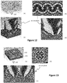
- Figures 12 and 13 show possible examples of such arrangements of moon-like nanojet microlenses.
- Figures 12(a) to 12(d) illustrate an alternate embodiment to the device of figure 3 , according to which several devices with a crescent-moon shape are assembled in order to form a periodic S-type curved groove in a host dielectric medium.
- Figure 12(a) presents a perspective view of a dielectric plate 121, within which a generalized crescent moon like focusing element having a form of a periodic S-type curved groove 122 is created. More precisely, figure 12(a) shows the topology of a unit cell of such a periodic groove, placed in free space 123, and engraved at the surface of a dielectric substrate 121.
- Figure 12(b) illustrates the near-field intensity pattern in xy-plane at a close distance above the plate surface 121.
- Figure 12(c) provides a 3D view of the field intensity pattern of the unit cell of figure 12(a) .
- Figure 12(d) illustrates the field intensity pattern in a 2D xz-plane crossing a nanojet beam.
- Figures 13(a) to 13(c) illustrate a further alternate embodiment, according to which several devices with a crescent moon shape are assembled in order to form a cavity with a gear-type cross section with four identical concave segments, created in a double-layer dielectric plate.
- figure 13(a) illustrates the topology of such a gear-type cavity 132, created in a dielectric plate 131.
- Figure 13(b) shows the near-field intensity pattern in xy-plane at a close distance above the plate 131 surface;
- figure 13(c) shows the field intensity pattern in xz-plane passing through the center of the cavity 132 and its concave segments.
- the host medium refractive index n 1 1.5
- such devices embedding one or several cavities with a crescent moon shape in a dielectric microstructure can be fabricated using any established microfabrication technique, like molding (e.g. nanoimprinting) or photolithography.
- such a component can take the form of a plate made of an optically transparent material (e.g. glass, plastic, polymer) with a microstructure formed on one of its surfaces.
- the plate can be planar or curved, flexible (bendable).
- the plate can be made of a single material or may comprise several layers. The former option is more suitable for resist-free molding fabrication methods, while the latter is more relevant to photolithography techniques.
- the plate with engraved microstructure can be attached to another component, e.g. another dielectric plate or a plano-convex lens.
- the nanojet cavities may be formed on the external surface of the compound component, or at the interface between the two attached components.
- the proposed component in all its embodiments, can be, for instance, fabricated in the form of a thin film with perforated apertures attached to a glass plate or directly to a surface of another optical component, e.g. a plano-convex lens. It can also be covered with another layer of an optically-transparent media (e.g. another glass plate).
- the film can be made of an optically transparent material, like PMMA (Acrylic), that is to be deposited directly on the surface of the supporting component (e.g. glass plate or lens). For instance, this can be done by spin-coating that enables deposition of thin nanofilms with the desired thickness (order of a few hundred nanometers).
- the apertures (that will serve as hollow cuboids) can then be created, for instance, using the optical or e-beam lithography technology.
- the periodic structures can be, potentially, fabricated using the maskless interference lithography that is faster and cheaper than standard optical lithography.
- the cavities with a crescent moon shape can be fabricated using nanoimprinting or replica molding methods in an optically transparent material, e.g. soft organic polymer such as PDMS, and then attached to a surface of a glass plate acting as a support.
- an optically transparent material e.g. soft organic polymer such as PDMS
- Figure 14 presents an example of a device that can be used to control the performance of a device according to one embodiment of the disclosure.
- Such a device referenced 1400 comprises a computing unit (for example a CPU, for "Central Processing Unit”), referenced 1401, and one or more memory units (for example a RAM (for " Random Access Memory ”) block in which intermediate results can be stored temporarily during the execution of instructions a computer program, or a ROM block in which, among other things, computer programs are stored, or an EEPROM (“ Electrically-Erasable Programmable Read-Only Memory ”) block, or a flash block) referenced 1402. Computer programs are made of instructions that can be executed by the computing unit.
- a device 1400 can also comprise a dedicated unit, referenced 1403, constituting an input-output interface to allow the device 1400 to communicate with other devices.
- this dedicated unit 1403 can be connected with an antenna (in order to perform communication without contacts), with light source/receiving unit (such as for example a photodiode, optical fiber, detector, e.g. photodiode, etc.) or with serial ports (to carry communications "contact").
- light source/receiving unit such as for example a photodiode, optical fiber, detector, e.g. photodiode, etc.
- serial ports to carry communications "contact”
- control of the performance of a device can be implemented in hardware in a programmable FPGA (" Field Programmable Gate Array ”) component or ASIC (" Application-Specific Integrated Circuit ”) component.
- a programmable FPGA Field Programmable Gate Array
- ASIC Application-Specific Integrated Circuit
Priority Applications (5)
| Application Number | Priority Date | Filing Date | Title |
|---|---|---|---|
| EP16306387.8A EP3312660A1 (de) | 2016-10-21 | 2016-10-21 | Vorrichtung zur bildung von mindestens einem geneigten fokussierten strahl im nahbereich aus einfallenden elektromagnetischen wellen |
| CN201780064815.8A CN110168432B (zh) | 2016-10-21 | 2017-10-20 | 用于由入射电磁波在近区形成至少一个倾斜聚焦束的设备 |
| US16/342,036 US11275252B2 (en) | 2016-10-21 | 2017-10-20 | Device for forming at least one tilted focused beam in the near zone, from incident electromagnetic waves |
| PCT/EP2017/076877 WO2018073426A1 (en) | 2016-10-21 | 2017-10-20 | Device for forming at least one tilted focused beam in the near zone, from incident electromagnetic waves |
| EP17784325.7A EP3529657B1 (de) | 2016-10-21 | 2017-10-20 | Vorrichtung zur bildung von mindestens einem geneigten fokussierten strahl im nahbereich aus einfallenden elektromagnetischen wellen |
Applications Claiming Priority (1)
| Application Number | Priority Date | Filing Date | Title |
|---|---|---|---|
| EP16306387.8A EP3312660A1 (de) | 2016-10-21 | 2016-10-21 | Vorrichtung zur bildung von mindestens einem geneigten fokussierten strahl im nahbereich aus einfallenden elektromagnetischen wellen |
Publications (1)
| Publication Number | Publication Date |
|---|---|
| EP3312660A1 true EP3312660A1 (de) | 2018-04-25 |
Family
ID=57944243
Family Applications (2)
| Application Number | Title | Priority Date | Filing Date |
|---|---|---|---|
| EP16306387.8A Withdrawn EP3312660A1 (de) | 2016-10-21 | 2016-10-21 | Vorrichtung zur bildung von mindestens einem geneigten fokussierten strahl im nahbereich aus einfallenden elektromagnetischen wellen |
| EP17784325.7A Active EP3529657B1 (de) | 2016-10-21 | 2017-10-20 | Vorrichtung zur bildung von mindestens einem geneigten fokussierten strahl im nahbereich aus einfallenden elektromagnetischen wellen |
Family Applications After (1)
| Application Number | Title | Priority Date | Filing Date |
|---|---|---|---|
| EP17784325.7A Active EP3529657B1 (de) | 2016-10-21 | 2017-10-20 | Vorrichtung zur bildung von mindestens einem geneigten fokussierten strahl im nahbereich aus einfallenden elektromagnetischen wellen |
Country Status (4)
| Country | Link |
|---|---|
| US (1) | US11275252B2 (de) |
| EP (2) | EP3312660A1 (de) |
| CN (1) | CN110168432B (de) |
| WO (1) | WO2018073426A1 (de) |
Cited By (9)
| Publication number | Priority date | Publication date | Assignee | Title |
|---|---|---|---|---|
| EP3633438A1 (de) * | 2018-10-01 | 2020-04-08 | InterDigital CE Patent Holdings | Inhomogene mikrolinsenvorrichtung zur nahfeld-fokussierung, strahlformung und hocheffizienten fernfeldvorrichtungsimplementierung |
| EP3632564A1 (de) | 2018-10-01 | 2020-04-08 | Thomson Licensing | System zur optischen erkennung und bildgebung von nanoskaligen objekten |
| EP3671322A1 (de) | 2018-12-18 | 2020-06-24 | Thomson Licensing | Vorrichtung zur formung einer ausgehenden elektromagnetischen welle aus einer einfallenden elektromagnetischen welle |
| EP3671321A1 (de) | 2018-12-18 | 2020-06-24 | Thomson Licensing | Vorrichtung zur bildung von mindestens einem geneigten fokussierten strahl in der nahfeldzone aus einfallenden elektromagnetischen wellen und bildsensor mit solch einer vorrichtung |
| CN113056697A (zh) * | 2018-10-01 | 2021-06-29 | 交互数字Ce专利控股公司 | 用于近场聚焦和波束形成的装置 |
| CN113181556A (zh) * | 2021-04-30 | 2021-07-30 | 西北核技术研究所 | 一种增强大型效应物内场强的基于介质基底结构的辐照腔 |
| US11442198B2 (en) | 2017-09-01 | 2022-09-13 | Interdigital Ce Patent Holdings, Sas | Optical device capable of providing at least two different optical functions |
| US11573356B2 (en) | 2018-03-13 | 2023-02-07 | Interdigital Ce Patent Holdings | Diffraction grating comprising double-materials structures |
| US11604363B2 (en) | 2018-03-13 | 2023-03-14 | Interdigital Ce Patent Holdings | Image sensor comprising a color splitter with two different refractive indexes |
Families Citing this family (12)
| Publication number | Priority date | Publication date | Assignee | Title |
|---|---|---|---|---|
| EP3223063A1 (de) | 2016-03-24 | 2017-09-27 | Thomson Licensing | Vorrichtung zur bildung von einem feldintensitätsmuster im nahbereich aus einfallenden elektromagnetischen wellen |
| EP3312646A1 (de) | 2016-10-21 | 2018-04-25 | Thomson Licensing | Vorrichtung und verfahren zur abschirmung von mindestens einem sub-wellenlängen-skala-objekt von einer einfallenden elektromagnetischen welle |
| EP3312660A1 (de) | 2016-10-21 | 2018-04-25 | Thomson Licensing | Vorrichtung zur bildung von mindestens einem geneigten fokussierten strahl im nahbereich aus einfallenden elektromagnetischen wellen |
| US10242503B2 (en) | 2017-01-09 | 2019-03-26 | Snap Inc. | Surface aware lens |
| EP3385219B1 (de) | 2017-04-07 | 2021-07-14 | InterDigital CE Patent Holdings | Verfahren zur herstellung einer vorrichtung zum ausbilden wenigstens eines fokussierten strahls in einem nahbereich |
| US11030813B2 (en) | 2018-08-30 | 2021-06-08 | Snap Inc. | Video clip object tracking |
| US11176737B2 (en) | 2018-11-27 | 2021-11-16 | Snap Inc. | Textured mesh building |
| EP3671310A1 (de) * | 2018-12-18 | 2020-06-24 | Thomson Licensing | Optische manipulationsvorrichtung zum einfangen oder bewegen von mikro- oder nanopartikeln |
| WO2020132541A1 (en) | 2018-12-20 | 2020-06-25 | Snap Inc. | Virtual surface modification |
| US11189098B2 (en) * | 2019-06-28 | 2021-11-30 | Snap Inc. | 3D object camera customization system |
| CN110829035B (zh) * | 2019-11-19 | 2021-03-16 | 大连海事大学 | 一种宽半功率波束的圆极化贴片天线 |
| US11227442B1 (en) | 2019-12-19 | 2022-01-18 | Snap Inc. | 3D captions with semantic graphical elements |
Citations (7)
| Publication number | Priority date | Publication date | Assignee | Title |
|---|---|---|---|---|
| US7394535B1 (en) | 2007-03-20 | 2008-07-01 | Tokyo Electron Limited | Optical metrology using a photonic nanojet |
| US20100067842A1 (en) * | 2007-09-17 | 2010-03-18 | Seidman Abraham N | Steerable, thin far-field electromagnetic beam |
| JP2011014857A (ja) * | 2009-06-05 | 2011-01-20 | Nec Corp | 光学素子とこれを用いた光子発生装置、光発生装置、光記録装置および光検出装置 |
| US8003965B2 (en) | 2007-05-18 | 2011-08-23 | The Regents Of The University Of Michigan | Apparatus for sub-wavelength near-field focusing of electromagnetic waves |
| US8554031B2 (en) | 2009-06-17 | 2013-10-08 | University Of North Carolina At Charlotte | Focusing multimodal optical microprobe devices |
| US20140111677A1 (en) | 2012-10-19 | 2014-04-24 | Canon Kabushiki Kaisha | Image sensor and image capturing apparatus |
| US8953064B1 (en) | 2004-10-01 | 2015-02-10 | The Board Of Trustees Of The Leland Stanford Junior University | Imaging arrangements and methods therefor |
Family Cites Families (78)
| Publication number | Priority date | Publication date | Assignee | Title |
|---|---|---|---|---|
| US3873408A (en) | 1969-10-06 | 1975-03-25 | Bausch & Lomb | Method of producing a refractive index gradient in glass |
| US3718383A (en) | 1971-04-19 | 1973-02-27 | Eastman Kodak Co | Plastic optical element having refractive index gradient |
| US3904268A (en) | 1974-11-15 | 1975-09-09 | Corning Glass Works | Optical waveguide having optimal index gradient |
| FR2578658B1 (fr) | 1985-03-05 | 1990-06-01 | Nippon Sheet Glass Co Ltd | Plaque a microlentilles et son procede de fabrication |
| US6753131B1 (en) | 1996-07-22 | 2004-06-22 | President And Fellows Of Harvard College | Transparent elastomeric, contact-mode photolithography mask, sensor, and wavefront engineering element |
| WO1999015933A1 (en) | 1997-09-19 | 1999-04-01 | International Business Machines Corporation | Optical lithography beyond conventional resolution limits |
| US6236513B1 (en) | 1999-06-30 | 2001-05-22 | Quantum Corporation | Integrated objective/solid immersion lens for near field recording |
| CN100416306C (zh) * | 2000-02-02 | 2008-09-03 | 闪亮胶片有限责任公司 | 多反射光定向膜 |
| US6804189B2 (en) | 2000-04-07 | 2004-10-12 | Tosoh Corporation | Near field optical recording medium |
| US6594430B1 (en) | 2000-05-11 | 2003-07-15 | Carnegie Mellon University | Solid immersion lenses for focusing collimated light in the near-field region |
| AU2002327367A1 (en) | 2001-07-26 | 2003-02-17 | Chad Edward Bouton | Electromagnetic sensors for biological tissue applications |
| US7057151B2 (en) | 2001-08-31 | 2006-06-06 | Universite Louis Pasteur | Optical transmission apparatus with directionality and divergence control |
| WO2003025635A1 (en) | 2001-09-19 | 2003-03-27 | Technion Research & Development Foundation Ltd. | Space-variant subwavelength dielectric grating and applications thereof |
| ATE374493T1 (de) | 2002-03-29 | 2007-10-15 | Global Dataguard Inc | Adaptive verhaltensbezogene eindringdetektion |
| EP1398656A1 (de) | 2002-09-12 | 2004-03-17 | Olimatech Ltd. | Durch Oberflächenplasmonen erzeugte Lichtquelle und ihre Verwendung |
| US7190521B2 (en) | 2002-09-13 | 2007-03-13 | Technion Research And Development Foundation Ltd. | Space-variant subwavelength dielectric grating and applications thereof |
| CN1823456A (zh) | 2003-06-10 | 2006-08-23 | 福托纳米公司 | 在二阶或高阶分布反馈激光器中抑制空间烧孔的方法和设备 |
| WO2005029164A1 (ja) | 2003-09-18 | 2005-03-31 | Nec Corporation | 光学素子 |
| JP4824273B2 (ja) | 2003-11-07 | 2011-11-30 | 大日本印刷株式会社 | 回折格子作製用位相マスク |
| US7541115B1 (en) | 2004-11-15 | 2009-06-02 | Kla-Tencor Technologies Corporation | Use of calcium fluoride substrate for lithography masks |
| WO2006067734A1 (en) | 2004-12-22 | 2006-06-29 | Koninklijke Philips Electronics N.V. | Apparatus and method for enhanced optical transmission through a small aperture, using radially polarized radiation |
| US20090068597A1 (en) | 2005-01-14 | 2009-03-12 | Naomasa Shiraishi | Exposure method and apparatus, and electronic device manufacturing method |
| US9677856B2 (en) | 2006-07-25 | 2017-06-13 | Imperial Innovations Limited | Electromagnetic cloaking method |
| US8208502B2 (en) | 2006-10-03 | 2012-06-26 | California Institute Of Technology | Fiber-coupled solid state microcavity light emitters |
| WO2008069454A1 (en) | 2006-12-05 | 2008-06-12 | Electronics And Telecommunications Research Institute | Guided mode resonance filter including high refractive index organic material and optical biosensor including the guided mode resonance filter |
| WO2008085717A1 (en) | 2006-12-21 | 2008-07-17 | Annulex Inc. | Shutter system |
| US8448810B2 (en) | 2007-01-12 | 2013-05-28 | Millercoors, Llc | Double walled beverage container and method of making same |
| US7639351B2 (en) | 2007-03-20 | 2009-12-29 | Tokyo Electron Limited | Automated process control using optical metrology with a photonic nanojet |
| US8052908B2 (en) | 2007-05-02 | 2011-11-08 | University Of Maryland | Photolithographic mask exhibiting enhanced light transmission due to utilizing sub-wavelength aperture arrays for imaging patterns in nano-lithography |
| US7612883B2 (en) | 2007-05-17 | 2009-11-03 | General Electric Company | Dynamic plasmonics-enabled signal enhancement, a device comprising the same, and a method using the same |
| WO2009095835A2 (en) | 2008-01-31 | 2009-08-06 | Nxp B.V. | Fully insulated semiconductor device and a method of manufacturing the same |
| FR2931560B1 (fr) | 2008-05-20 | 2010-08-27 | Commissariat Energie Atomique | Dispositif de focalisation de lumiere a des dimensions sub-longueur d'onde a fort rendement |
| US8168939B2 (en) | 2008-07-09 | 2012-05-01 | Luxtera, Inc. | Method and system for a light source assembly supporting direct coupling to an integrated circuit |
| US8488247B2 (en) | 2008-10-06 | 2013-07-16 | Purdue Research Foundation | System, method and apparatus for modifying the visibility properties of an object |
| CN101419337B (zh) * | 2008-11-28 | 2011-12-14 | 中国科学技术大学 | 用于光斑三维压缩的超衍射相位调制片及其加工方法 |
| US9215423B2 (en) | 2009-03-30 | 2015-12-15 | Time Warner Cable Enterprises Llc | Recommendation engine apparatus and methods |
| WO2010114834A1 (en) | 2009-03-30 | 2010-10-07 | The Trustees Of The University Of Pennsylvania | Cloaked sensor |
| US8634140B2 (en) | 2009-04-17 | 2014-01-21 | The Invention Science Fund I Llc | Evanescent electromagnetic wave conversion apparatus III |
| US8786852B2 (en) | 2009-12-02 | 2014-07-22 | Lawrence Livermore National Security, Llc | Nanoscale array structures suitable for surface enhanced raman scattering and methods related thereto |
| US9151891B2 (en) | 2010-02-12 | 2015-10-06 | The Regents Of The University Of California | Metamaterial-based optical lenses |
| CN101819326B (zh) | 2010-04-15 | 2011-08-31 | 北京交通大学 | 用于形成空心光束的光子晶体光纤耦合器及其制备方法 |
| KR101274068B1 (ko) | 2010-05-25 | 2013-06-12 | 서울대학교산학협력단 | 양자점 발광 소자 및 이를 이용한 디스플레이 |
| AU2011281097B2 (en) | 2010-07-22 | 2015-11-26 | University Of Pittsburgh - Of The Commonwealth System Of Higher Education | Nano-optic refractive optics |
| KR20120111288A (ko) | 2011-03-31 | 2012-10-10 | 국민대학교산학협력단 | 나노 임프린트용 몰드와 포토 마스크를 동시에 이용한 미세 패턴 형성 방법 |
| US8508830B1 (en) | 2011-05-13 | 2013-08-13 | Google Inc. | Quantum dot near-to-eye display |
| US8487425B2 (en) | 2011-06-23 | 2013-07-16 | International Business Machines Corporation | Optimized annular copper TSV |
| CN102916343B (zh) | 2011-08-05 | 2015-07-15 | 苏州大学 | 一种量子点材料的制作装置及制作方法 |
| WO2013049367A2 (en) | 2011-09-30 | 2013-04-04 | Rolith, Inc. | Plasmonic lithography using phase mask |
| US9170203B2 (en) | 2012-05-16 | 2015-10-27 | Indian Institute Of Technology Madras | Enhancement of raman scattering |
| US20130335677A1 (en) | 2012-06-15 | 2013-12-19 | Apple Inc. | Quantum Dot-Enhanced Display Having Dichroic Filter |
| US9140602B2 (en) | 2012-08-11 | 2015-09-22 | The Board Of Trustees Of The Leland Stanford Junior University | Nanophotonic light-field sensor |
| NZ710096A (en) | 2013-01-15 | 2018-11-30 | Magic Leap Inc | Ultra-high resolution scanning fiber display |
| US9739709B2 (en) | 2013-05-08 | 2017-08-22 | Colorado State University Research Foundation | Hydrocarbon sensing methods and apparatus |
| CN103353675B (zh) | 2013-07-02 | 2015-11-11 | 浙江大学 | 基于微结构的移频超分辨显微成像方法和装置 |
| WO2015008365A1 (ja) | 2013-07-18 | 2015-01-22 | ギガフォトン株式会社 | 露光装置 |
| EP3051351B1 (de) | 2013-09-24 | 2019-06-12 | Institute of Optics and Electronics Chinese Academy of Sciences | Fotoätzung von bildern mit sehr hoher auflösung |
| JP6356557B2 (ja) | 2013-09-30 | 2018-07-11 | 株式会社豊田中央研究所 | レンズおよびその製造方法 |
| KR101573724B1 (ko) | 2013-11-22 | 2015-12-02 | 한국과학기술연구원 | 나노안테나 배열의 제조 방법, 나노안테나 배열 칩 및 리소그래피용 구조물 |
| KR102651578B1 (ko) | 2013-11-27 | 2024-03-25 | 매직 립, 인코포레이티드 | 가상 및 증강 현실 시스템들 및 방법들 |
| FR3014177B1 (fr) * | 2013-12-04 | 2019-05-17 | Commissariat A L'energie Atomique Et Aux Energies Alternatives | Structure de surface pour les absorbeurs solaires thermiques et leur procede de realisation. |
| US9651718B2 (en) | 2014-01-27 | 2017-05-16 | Forelux Inc. | Photonic apparatus with periodic structures |
| US10176562B2 (en) | 2014-02-24 | 2019-01-08 | Rambus Inc. | Optical flow sensing and pattern recognition with anti-symmetric phase gratings |
| US9389424B1 (en) | 2014-04-02 | 2016-07-12 | Magic Leap, Inc. | Methods and systems for implementing a high resolution color micro-display |
| EP3194934B1 (de) | 2014-08-08 | 2024-03-06 | Quantum-Si Incorporated | Integrierte vorrichtung zur verwendung mit einer externen lichtquelle zur sondierung, detektion und analyse von molekülen mittels lumineszenzlebensdauermessungen |
| US9709884B2 (en) | 2014-11-26 | 2017-07-18 | Taiwan Semiconductor Manufacturing Company, Ltd. | EUV mask and manufacturing method by using the same |
| KR102279386B1 (ko) | 2015-02-03 | 2021-07-21 | 삼성전자주식회사 | 디스플레이 장치 |
| US20160240419A1 (en) * | 2015-02-13 | 2016-08-18 | Eastman Kodak Company | Atomic-layer deposition substrate |
| JP6569856B2 (ja) | 2015-03-13 | 2019-09-04 | パナソニックIpマネジメント株式会社 | 発光装置および内視鏡 |
| US10182702B2 (en) | 2015-03-13 | 2019-01-22 | Panasonic Intellectual Property Management Co., Ltd. | Light-emitting apparatus including photoluminescent layer |
| RU2591282C1 (ru) | 2015-04-30 | 2016-07-20 | Федеральное государственное бюджетное образовательное учреждение высшего образования "Сибирский государственный университет геосистем и технологий" (СГУГиТ) | Устройство квазиоптической линии передачи терагерцовых волн |
| WO2017007431A1 (en) | 2015-07-09 | 2017-01-12 | National University Of Singapore | Microsphere for generating a photonic nanojet |
| EP3223062A1 (de) | 2016-03-24 | 2017-09-27 | Thomson Licensing | Vorrichtung zur bildung von mindestens einem fokussierten strahl im nahbereich aus einfallenden elektromagnetischen wellen |
| EP3223063A1 (de) | 2016-03-24 | 2017-09-27 | Thomson Licensing | Vorrichtung zur bildung von einem feldintensitätsmuster im nahbereich aus einfallenden elektromagnetischen wellen |
| EP3312660A1 (de) | 2016-10-21 | 2018-04-25 | Thomson Licensing | Vorrichtung zur bildung von mindestens einem geneigten fokussierten strahl im nahbereich aus einfallenden elektromagnetischen wellen |
| EP3312674A1 (de) | 2016-10-21 | 2018-04-25 | Thomson Licensing | Fotolithografische vorrichtung zum erzeugen eines musters auf einem fotoresistsubstrat |
| EP3312646A1 (de) | 2016-10-21 | 2018-04-25 | Thomson Licensing | Vorrichtung und verfahren zur abschirmung von mindestens einem sub-wellenlängen-skala-objekt von einer einfallenden elektromagnetischen welle |
| EP3385219B1 (de) | 2017-04-07 | 2021-07-14 | InterDigital CE Patent Holdings | Verfahren zur herstellung einer vorrichtung zum ausbilden wenigstens eines fokussierten strahls in einem nahbereich |
| EP3460561A1 (de) | 2017-09-26 | 2019-03-27 | Thomson Licensing | Vorrichtung zur ablenkung und fokussierung von licht |
-
2016
- 2016-10-21 EP EP16306387.8A patent/EP3312660A1/de not_active Withdrawn
-
2017
- 2017-10-20 US US16/342,036 patent/US11275252B2/en active Active
- 2017-10-20 EP EP17784325.7A patent/EP3529657B1/de active Active
- 2017-10-20 WO PCT/EP2017/076877 patent/WO2018073426A1/en unknown
- 2017-10-20 CN CN201780064815.8A patent/CN110168432B/zh active Active
Patent Citations (7)
| Publication number | Priority date | Publication date | Assignee | Title |
|---|---|---|---|---|
| US8953064B1 (en) | 2004-10-01 | 2015-02-10 | The Board Of Trustees Of The Leland Stanford Junior University | Imaging arrangements and methods therefor |
| US7394535B1 (en) | 2007-03-20 | 2008-07-01 | Tokyo Electron Limited | Optical metrology using a photonic nanojet |
| US8003965B2 (en) | 2007-05-18 | 2011-08-23 | The Regents Of The University Of Michigan | Apparatus for sub-wavelength near-field focusing of electromagnetic waves |
| US20100067842A1 (en) * | 2007-09-17 | 2010-03-18 | Seidman Abraham N | Steerable, thin far-field electromagnetic beam |
| JP2011014857A (ja) * | 2009-06-05 | 2011-01-20 | Nec Corp | 光学素子とこれを用いた光子発生装置、光発生装置、光記録装置および光検出装置 |
| US8554031B2 (en) | 2009-06-17 | 2013-10-08 | University Of North Carolina At Charlotte | Focusing multimodal optical microprobe devices |
| US20140111677A1 (en) | 2012-10-19 | 2014-04-24 | Canon Kabushiki Kaisha | Image sensor and image capturing apparatus |
Non-Patent Citations (15)
| Title |
|---|
| A. GRBIC; L. JIANG; R. MERLIN: "Near-field plates: subdiffraction focusing with patterned surfaces", SCIENCE, vol. 320, 2008, pages 511 - 513 |
| A. HEIFETZ ET AL.: "Photonic ngnojets", JOURNAL OF COMPUTATIONAL THEORY NANOSCIENCE, vol. 6, 2009, pages 1979 - 1992 |
| ABDUL KHALEQUE ET AL: "TAILORING THE PROPERTIES OF PHOTONIC NANOJETS BY CHANGING THE MATERIAL AND GEOMETRY OF THE CONCENTRATOR", PROGRESS IN ELECTROMAGNETICS RESEARCH LETTERS, vol. 48, 1 January 2014 (2014-01-01), pages 7 - 13, XP055358699, DOI: 10.2528/PIERL14052108 * |
| BORISKINA S V: "Spectrally engineered photonic molecules as optical sensors with enhanced sensitivity: a proposal and numerical analysis", JOURNAL OF THE OPTICAL SOCIETY OF AMERICA - B, OPTICAL SOCIETY OF AMERICA, WASHINGTON, US, vol. 23, no. 8, 1 August 2006 (2006-08-01), pages 1565 - 1573, XP002599445, ISSN: 0740-3224 * |
| GEINTS YU E ET AL: "Modeling spatially localized photonic nanojets from phase diffraction gratings", JOURNAL OF APPLIED PHYSICS, AMERICAN INSTITUTE OF PHYSICS, US, vol. 119, no. 15, 21 April 2016 (2016-04-21), XP012206957, ISSN: 0021-8979, [retrieved on 19010101], DOI: 10.1063/1.4946846 * |
| H. HUA; B. JAVADI: "A 3D inteGral imaging optical see-through head-mounted displgy", OPT. EXPRESS, vol. 22, 2014, pages 13484 |
| H. MUKAWA ET AL.: "A full -color evewear display using planar waveguides with reflection volume holograms", PROCEEDINGS OF SID, vol. 17, no. 3, 2009, pages 185 - 193 |
| L. NOVOTNY; S.J. STRANICK: "Near-field optical microscopy and spectroscopy with pointed probes", ANNU. REV. PHYS. CHEM., vol. 57, 2006, pages 303 - 331 |
| LIU CHENG-YANG ET AL: "Geometric effect on photonic nanojet generated by dielectric microcylinders with non-cylindrical cross-sections", OPTICS COMMUNICATIONS, ELSEVIER, AMSTERDAM, NL, vol. 380, 17 June 2016 (2016-06-17), pages 287 - 296, XP029694296, ISSN: 0030-4018, DOI: 10.1016/J.OPTCOM.2016.06.021 * |
| LIU CHENG-YANG ET AL: "Photonic nanojet modulation by elliptical microcylinders", OPTIK, vol. 125, no. 15, 18 April 2014 (2014-04-18), pages 4043 - 4046, XP029034403, ISSN: 0030-4026, DOI: 10.1016/J.IJLEO.2014.01.116 * |
| S. NISHIWAKI ET AL.: "Efficient colour splitters for high-pixel density imaGe sensors", NATURE PHOTONICS, vol. 7, 2013, pages 240 - 246 |
| S.-C. KONG ET AL.: "Photonic nanoiet-enabled optical data storgge", OPT. EXPRESS, vol. 16, no. 18, 2008 |
| S.Y. GUO; J.M. LEDUE; P. GRUTTER: "Fabrication of optical fiber probes for scanning near-field optical microscopy", MSURJ, vol. 3, no. 1, 2008 |
| V. PACHECO-PENA ET AL.: "Multifre uencv focusing and wide angular scanning of teraiets", OPT. LETT., vol. 40, no. 2, 2015, pages 245 - 248 |
| V. PACHECO-PENA ET AL.: "Teraiets produced by dielectric cuboids", APPLIED PHYS. LETT., vol. 105, 2014, pages 084102 |
Cited By (16)
| Publication number | Priority date | Publication date | Assignee | Title |
|---|---|---|---|---|
| US11442198B2 (en) | 2017-09-01 | 2022-09-13 | Interdigital Ce Patent Holdings, Sas | Optical device capable of providing at least two different optical functions |
| US11604363B2 (en) | 2018-03-13 | 2023-03-14 | Interdigital Ce Patent Holdings | Image sensor comprising a color splitter with two different refractive indexes |
| US11573356B2 (en) | 2018-03-13 | 2023-02-07 | Interdigital Ce Patent Holdings | Diffraction grating comprising double-materials structures |
| CN113056697A (zh) * | 2018-10-01 | 2021-06-29 | 交互数字Ce专利控股公司 | 用于近场聚焦和波束形成的装置 |
| CN113056698A (zh) * | 2018-10-01 | 2021-06-29 | 交互数字Ce专利控股公司 | 用于近场聚焦、光束形成和高效远场器件实现的非均质微透镜器件 |
| EP3633438A1 (de) * | 2018-10-01 | 2020-04-08 | InterDigital CE Patent Holdings | Inhomogene mikrolinsenvorrichtung zur nahfeld-fokussierung, strahlformung und hocheffizienten fernfeldvorrichtungsimplementierung |
| WO2020069963A1 (en) | 2018-10-01 | 2020-04-09 | Thomson Licensing | System for optical detection and imaging of nanoscale objects |
| WO2020070129A1 (en) * | 2018-10-01 | 2020-04-09 | Interdigital Ce Patent Holdings | Inhomogeneous microlens device for near-field focusing, beam forming, and high-efficiency far-field device implementation |
| EP3632564A1 (de) | 2018-10-01 | 2020-04-08 | Thomson Licensing | System zur optischen erkennung und bildgebung von nanoskaligen objekten |
| CN113056698B (zh) * | 2018-10-01 | 2023-11-03 | 交互数字Ce专利控股公司 | 用于近场聚焦、光束形成和高效远场器件实现的非均质微透镜器件 |
| CN113056697B (zh) * | 2018-10-01 | 2023-11-03 | 交互数字Ce专利控股公司 | 用于近场聚焦和波束形成的装置 |
| EP3671322A1 (de) | 2018-12-18 | 2020-06-24 | Thomson Licensing | Vorrichtung zur formung einer ausgehenden elektromagnetischen welle aus einer einfallenden elektromagnetischen welle |
| EP3671321A1 (de) | 2018-12-18 | 2020-06-24 | Thomson Licensing | Vorrichtung zur bildung von mindestens einem geneigten fokussierten strahl in der nahfeldzone aus einfallenden elektromagnetischen wellen und bildsensor mit solch einer vorrichtung |
| WO2020127150A1 (en) * | 2018-12-18 | 2020-06-25 | Interdigital Ce Patent Holdings | Device for forming an outgoing electromagnetic wave from an incident electromagnetic wave |
| CN113383265A (zh) * | 2018-12-18 | 2021-09-10 | 交互数字Ce专利控股公司 | 用于从入射电磁波形成输出电磁波的器件 |
| CN113181556A (zh) * | 2021-04-30 | 2021-07-30 | 西北核技术研究所 | 一种增强大型效应物内场强的基于介质基底结构的辐照腔 |
Also Published As
| Publication number | Publication date |
|---|---|
| WO2018073426A1 (en) | 2018-04-26 |
| US20200348526A1 (en) | 2020-11-05 |
| EP3529657B1 (de) | 2021-12-15 |
| EP3529657A1 (de) | 2019-08-28 |
| US11275252B2 (en) | 2022-03-15 |
| WO2018073426A9 (en) | 2018-09-07 |
| CN110168432A (zh) | 2019-08-23 |
| CN110168432B (zh) | 2021-09-28 |
Similar Documents
| Publication | Publication Date | Title |
|---|---|---|
| EP3529657B1 (de) | Vorrichtung zur bildung von mindestens einem geneigten fokussierten strahl im nahbereich aus einfallenden elektromagnetischen wellen | |
| US10677992B2 (en) | Device for forming at least one focused beam in the near zone, from incident electromagnetic waves | |
| US11163175B2 (en) | Device for forming a field intensity pattern in the near zone, from incident electromagnetic waves | |
| US11573356B2 (en) | Diffraction grating comprising double-materials structures | |
| EP3385219B1 (de) | Verfahren zur herstellung einer vorrichtung zum ausbilden wenigstens eines fokussierten strahls in einem nahbereich | |
| US20210389597A1 (en) | Device for near-field focusing and beam forming | |
| CN113056698B (zh) | 用于近场聚焦、光束形成和高效远场器件实现的非均质微透镜器件 | |
| Ozdemir | High Efficient Ultra-Thin Flat Optics Based on Dielectric Metasurfaces | |
| CN115943329A (zh) | 包括阶梯状腔的高颜色均匀性双材料衍射光栅 | |
| EP3671321A1 (de) | Vorrichtung zur bildung von mindestens einem geneigten fokussierten strahl in der nahfeldzone aus einfallenden elektromagnetischen wellen und bildsensor mit solch einer vorrichtung |
Legal Events
| Date | Code | Title | Description |
|---|---|---|---|
| PUAI | Public reference made under article 153(3) epc to a published international application that has entered the european phase |
Free format text: ORIGINAL CODE: 0009012 |
|
| AK | Designated contracting states |
Kind code of ref document: A1 Designated state(s): AL AT BE BG CH CY CZ DE DK EE ES FI FR GB GR HR HU IE IS IT LI LT LU LV MC MK MT NL NO PL PT RO RS SE SI SK SM TR |
|
| AX | Request for extension of the european patent |
Extension state: BA ME |
|
| STAA | Information on the status of an ep patent application or granted ep patent |
Free format text: STATUS: THE APPLICATION IS DEEMED TO BE WITHDRAWN |
|
| 18D | Application deemed to be withdrawn |
Effective date: 20181026 |
|
| RIN1 | Information on inventor provided before grant (corrected) |
Inventor name: BLONDE, LAURENT Inventor name: BORISKIN, ARTEM Inventor name: DRAZIC, VALTER |