EP3312011A1 - Fluid ejection head and method for making fluid ejection head - Google Patents
Fluid ejection head and method for making fluid ejection head Download PDFInfo
- Publication number
- EP3312011A1 EP3312011A1 EP17195399.5A EP17195399A EP3312011A1 EP 3312011 A1 EP3312011 A1 EP 3312011A1 EP 17195399 A EP17195399 A EP 17195399A EP 3312011 A1 EP3312011 A1 EP 3312011A1
- Authority
- EP
- European Patent Office
- Prior art keywords
- layer
- photoresist layer
- substrate
- photoresist
- fluid ejection
- Prior art date
- Legal status (The legal status is an assumption and is not a legal conclusion. Google has not performed a legal analysis and makes no representation as to the accuracy of the status listed.)
- Granted
Links
Images


Classifications
-
- B—PERFORMING OPERATIONS; TRANSPORTING
- B41—PRINTING; LINING MACHINES; TYPEWRITERS; STAMPS
- B41J—TYPEWRITERS; SELECTIVE PRINTING MECHANISMS, i.e. MECHANISMS PRINTING OTHERWISE THAN FROM A FORME; CORRECTION OF TYPOGRAPHICAL ERRORS
- B41J2/00—Typewriters or selective printing mechanisms characterised by the printing or marking process for which they are designed
- B41J2/005—Typewriters or selective printing mechanisms characterised by the printing or marking process for which they are designed characterised by bringing liquid or particles selectively into contact with a printing material
- B41J2/01—Ink jet
- B41J2/135—Nozzles
- B41J2/16—Production of nozzles
- B41J2/1601—Production of bubble jet print heads
- B41J2/1603—Production of bubble jet print heads of the front shooter type
-
- B—PERFORMING OPERATIONS; TRANSPORTING
- B41—PRINTING; LINING MACHINES; TYPEWRITERS; STAMPS
- B41J—TYPEWRITERS; SELECTIVE PRINTING MECHANISMS, i.e. MECHANISMS PRINTING OTHERWISE THAN FROM A FORME; CORRECTION OF TYPOGRAPHICAL ERRORS
- B41J2/00—Typewriters or selective printing mechanisms characterised by the printing or marking process for which they are designed
- B41J2/005—Typewriters or selective printing mechanisms characterised by the printing or marking process for which they are designed characterised by bringing liquid or particles selectively into contact with a printing material
- B41J2/01—Ink jet
- B41J2/135—Nozzles
- B41J2/14—Structure thereof only for on-demand ink jet heads
-
- B—PERFORMING OPERATIONS; TRANSPORTING
- B05—SPRAYING OR ATOMISING IN GENERAL; APPLYING FLUENT MATERIALS TO SURFACES, IN GENERAL
- B05B—SPRAYING APPARATUS; ATOMISING APPARATUS; NOZZLES
- B05B1/00—Nozzles, spray heads or other outlets, with or without auxiliary devices such as valves, heating means
- B05B1/02—Nozzles, spray heads or other outlets, with or without auxiliary devices such as valves, heating means designed to produce a jet, spray, or other discharge of particular shape or nature, e.g. in single drops, or having an outlet of particular shape
-
- B—PERFORMING OPERATIONS; TRANSPORTING
- B41—PRINTING; LINING MACHINES; TYPEWRITERS; STAMPS
- B41J—TYPEWRITERS; SELECTIVE PRINTING MECHANISMS, i.e. MECHANISMS PRINTING OTHERWISE THAN FROM A FORME; CORRECTION OF TYPOGRAPHICAL ERRORS
- B41J2/00—Typewriters or selective printing mechanisms characterised by the printing or marking process for which they are designed
- B41J2/005—Typewriters or selective printing mechanisms characterised by the printing or marking process for which they are designed characterised by bringing liquid or particles selectively into contact with a printing material
- B41J2/01—Ink jet
- B41J2/135—Nozzles
- B41J2/14—Structure thereof only for on-demand ink jet heads
- B41J2/1433—Structure of nozzle plates
-
- B—PERFORMING OPERATIONS; TRANSPORTING
- B41—PRINTING; LINING MACHINES; TYPEWRITERS; STAMPS
- B41J—TYPEWRITERS; SELECTIVE PRINTING MECHANISMS, i.e. MECHANISMS PRINTING OTHERWISE THAN FROM A FORME; CORRECTION OF TYPOGRAPHICAL ERRORS
- B41J2/00—Typewriters or selective printing mechanisms characterised by the printing or marking process for which they are designed
- B41J2/005—Typewriters or selective printing mechanisms characterised by the printing or marking process for which they are designed characterised by bringing liquid or particles selectively into contact with a printing material
- B41J2/01—Ink jet
- B41J2/135—Nozzles
- B41J2/16—Production of nozzles
- B41J2/1621—Manufacturing processes
- B41J2/1626—Manufacturing processes etching
- B41J2/1628—Manufacturing processes etching dry etching
-
- B—PERFORMING OPERATIONS; TRANSPORTING
- B41—PRINTING; LINING MACHINES; TYPEWRITERS; STAMPS
- B41J—TYPEWRITERS; SELECTIVE PRINTING MECHANISMS, i.e. MECHANISMS PRINTING OTHERWISE THAN FROM A FORME; CORRECTION OF TYPOGRAPHICAL ERRORS
- B41J2/00—Typewriters or selective printing mechanisms characterised by the printing or marking process for which they are designed
- B41J2/005—Typewriters or selective printing mechanisms characterised by the printing or marking process for which they are designed characterised by bringing liquid or particles selectively into contact with a printing material
- B41J2/01—Ink jet
- B41J2/135—Nozzles
- B41J2/16—Production of nozzles
- B41J2/1621—Manufacturing processes
- B41J2/1631—Manufacturing processes photolithography
-
- B—PERFORMING OPERATIONS; TRANSPORTING
- B41—PRINTING; LINING MACHINES; TYPEWRITERS; STAMPS
- B41J—TYPEWRITERS; SELECTIVE PRINTING MECHANISMS, i.e. MECHANISMS PRINTING OTHERWISE THAN FROM A FORME; CORRECTION OF TYPOGRAPHICAL ERRORS
- B41J2/00—Typewriters or selective printing mechanisms characterised by the printing or marking process for which they are designed
- B41J2/005—Typewriters or selective printing mechanisms characterised by the printing or marking process for which they are designed characterised by bringing liquid or particles selectively into contact with a printing material
- B41J2/01—Ink jet
- B41J2/135—Nozzles
- B41J2/16—Production of nozzles
- B41J2/1621—Manufacturing processes
- B41J2/1637—Manufacturing processes molding
- B41J2/1639—Manufacturing processes molding sacrificial molding
-
- B—PERFORMING OPERATIONS; TRANSPORTING
- B41—PRINTING; LINING MACHINES; TYPEWRITERS; STAMPS
- B41J—TYPEWRITERS; SELECTIVE PRINTING MECHANISMS, i.e. MECHANISMS PRINTING OTHERWISE THAN FROM A FORME; CORRECTION OF TYPOGRAPHICAL ERRORS
- B41J2/00—Typewriters or selective printing mechanisms characterised by the printing or marking process for which they are designed
- B41J2/005—Typewriters or selective printing mechanisms characterised by the printing or marking process for which they are designed characterised by bringing liquid or particles selectively into contact with a printing material
- B41J2/01—Ink jet
- B41J2/135—Nozzles
- B41J2/16—Production of nozzles
- B41J2/1621—Manufacturing processes
- B41J2/164—Manufacturing processes thin film formation
- B41J2/1645—Manufacturing processes thin film formation thin film formation by spincoating
-
- H—ELECTRICITY
- H10—SEMICONDUCTOR DEVICES; ELECTRIC SOLID-STATE DEVICES NOT OTHERWISE PROVIDED FOR
- H10N—ELECTRIC SOLID-STATE DEVICES NOT OTHERWISE PROVIDED FOR
- H10N30/00—Piezoelectric or electrostrictive devices
- H10N30/01—Manufacture or treatment
- H10N30/03—Assembling devices that include piezoelectric or electrostrictive parts
-
- H—ELECTRICITY
- H10—SEMICONDUCTOR DEVICES; ELECTRIC SOLID-STATE DEVICES NOT OTHERWISE PROVIDED FOR
- H10N—ELECTRIC SOLID-STATE DEVICES NOT OTHERWISE PROVIDED FOR
- H10N30/00—Piezoelectric or electrostrictive devices
- H10N30/01—Manufacture or treatment
- H10N30/07—Forming of piezoelectric or electrostrictive parts or bodies on an electrical element or another base
- H10N30/072—Forming of piezoelectric or electrostrictive parts or bodies on an electrical element or another base by laminating or bonding of piezoelectric or electrostrictive bodies
-
- H—ELECTRICITY
- H10—SEMICONDUCTOR DEVICES; ELECTRIC SOLID-STATE DEVICES NOT OTHERWISE PROVIDED FOR
- H10N—ELECTRIC SOLID-STATE DEVICES NOT OTHERWISE PROVIDED FOR
- H10N30/00—Piezoelectric or electrostrictive devices
- H10N30/01—Manufacture or treatment
- H10N30/08—Shaping or machining of piezoelectric or electrostrictive bodies
- H10N30/082—Shaping or machining of piezoelectric or electrostrictive bodies by etching, e.g. lithography
-
- H—ELECTRICITY
- H10—SEMICONDUCTOR DEVICES; ELECTRIC SOLID-STATE DEVICES NOT OTHERWISE PROVIDED FOR
- H10N—ELECTRIC SOLID-STATE DEVICES NOT OTHERWISE PROVIDED FOR
- H10N30/00—Piezoelectric or electrostrictive devices
- H10N30/80—Constructional details
- H10N30/88—Mounts; Supports; Enclosures; Casings
- H10N30/883—Additional insulation means preventing electrical, physical or chemical damage, e.g. protective coatings
Definitions
- the disclosure relates to fluid ejection devices, and in particular to improved methods for making fluid ejection head structures.
- Fluid ejection heads are useful for ejecting a variety of fluids including inks, cooling fluids, pharmaceuticals, lubricants and the like.
- a widely used fluid ejection head is in an inkjet printer.
- fluid ejection heads may also be used in vaporization devices for vapor therapy, E-cigarettes and the like. New techniques are constantly being developed to provide low cost, highly reliable fluid ejection heads for such devices.
- the fluid ejection head is a seemingly simple device that has a relatively complicated structure containing electrical circuits, ink passageways and a variety of tiny parts assembled with precision to provide a powerful, yet versatile fluid ejection head.
- the components of the ejection head must cooperate with each other and be useful for a variety of fluids and fluid formulations. Accordingly, it is important to match the ejection head components to the fluid being ejected. Slight variations in production quality can have a tremendous influence on the product yield and resulting ejection head performance.
- the primary components of a fluid ejection head are a semiconductor substrate, a flow feature layer, a nozzle plate layer, and a flexible circuit attached to the substrate.
- the semiconductor substrate is preferably made of silicon and contains various passivation layers, conductive metal layers, resistive layers, insulative layers and protective layers deposited on a device surface thereof.
- Fluid ejection actuators formed on a device surface of the substrate may be thermal actuators or piezoelectric actuators.
- individual heater resistors are defined in the resistive layers and each heater resistor corresponds to a nozzle hole in the nozzle plate for heating and ejecting fluid from the ejection head toward a desired substrate or target.
- the nozzle plate layer and the flow feature layer may each be made of a photo-imageable material.
- the flow feature layer is typically spin-coated onto the substrate, imaged and developed to provide flow features therein for directing fluid from a fluid via in the substrate to a heater on the substrate.
- the substrate is etched to form the fluid vias in a deep reactive ion etching (DRIE) process.
- DRIE deep reactive ion etching
- a dry film photoresist nozzle layer is then laminated to the flow feature layer using heated, pressure rollers. Finally, the nozzle layer is exposed and developed to form the nozzle holes therein.
- the nozzle plate layer is bridged across the fluid via in the substrate and the flow features in the flow feature layer. Stresses are introduced from the laminator rollers into the nozzle plate layer as the laminator roll radially compresses the nozzle plate layer, pushing the nozzle plate layer down into unsupported regions of the flow feature layer.
- the radial compression of the nozzle plate layer causes UV light diffraction during nozzle plate layer imaging, resulting in poor nozzle hole image quality.
- a second factor contributing to poor nozzle hole image quality is the fact that the heaters on the substrate are constructed of highly reflective material. The highly reflective material causes UV light rays used during nozzle plate imaging to reflect back into the nozzle plate layer photoresist material causing areas of the unexposed nozzle holes to be exposed to small amounts of UV radiation that results in misshapen nozzle holes.
- the planarity of the nozzle plate layer is critical to controlling fluid ejection directionality. Nozzle hole diameter variances also may cause drop mass inconsistencies. Accordingly, there continues to be a need for manufacturing processes and techniques which provide improved fluid ejection head components.
- the method of making a fluid ejection head includes steps of: providing a substrate, being configured to contain a plurality fluid ejection actuators on a device surface thereof; forming one or more fluid supply vias in the substrate; laminating a first photoresist layer to a device surface of the substrate; exposing the first photoresist layer to a first ultraviolet (UV) radiation through a first photo mask to provide a first UV exposed area of the first photoresist layer; heating the first photoresist layer to cross-link material in the first UV exposed area of the first photoresist layer; laminating a second photoresist layer to the first photoresist layer; exposing the second photoresist layer to a second UV radiation through a second photo mask to provide a second UV exposed area for nozzle holes; cross-linking the second photoresist layer with heat; and developing the first photoresist layer and second photo
- a fluid ejection head in another embodiment, there is provided a fluid ejection head.
- the fluid ejection head includes a substrate configured to contain a plurality of fluid ejection actuators on a device surface thereof and one or more fluid supply vias formed therethrough; a first photoresist layer, configured to be laminated to the device surface of the substrate; and a second photoresist layer, configured to be laminated to the first photoresist layer.
- the second photoresist layer includes: a hydrophilic photoresist material layer disposed adjacent to the first photoresist layer; and a hydrophobic photoresist material layer disposed adjacent to the hydrophilic photoresist material layer.
- the first photoresist layer is configured to provide an anti-reflective coating on the substrate. In another embodiment, the first photoresist layer is configured to have a thickness ranging from about 10 ⁇ m to about 30 ⁇ m.
- the second photoresist layer is configured to have a thickness ranging from about 10 ⁇ m to about 30.
- the hydrophilic photoresist material layer is configured to have a water contact angle ranging from about 60 degrees to less than about 90 degrees. In another embodiment, the hydrophobic photoresist material layer is configured to have a water contact angle ranging from about 91 degrees to about 120 degrees.
- the device surface of the substrate is configured to be plasma treated for promoting adhesion between the first photoresist layer and the device surface of the substrate.
- the first photoresist layer is configured to be plasma treated with oxygen and a forming gas to promote adhesion between the first photoresist layer and the second photoresist layer.
- the fluid ejection head is an inkjet print head.
- the first photoresist layer, or flow feature layer is effective to minimize stresses on the second photoresist layer, or nozzle plate layer, during a lamination process for the second photoresist layer.
- the first photoresist layer may be used as an anti-reflective layer between the second photoresist layer and highly reflective heater surfaces during an imaging step for the second photoresist layer.
- a reactive ion etching process for fluid supply vias in the substrate is conducted before the first photoresist layer is applied to the substrate thereby avoiding flow feature damage during the etching or striping processes, which would enable more aggressive strip processes for higher fluid ejection head yields.
- the fluid ejection head 10 includes a substrate 12 that is preferably a silicon semiconductor substrate containing a plurality of fluid ejection actuators such as piezoelectric devices or heater resistors 14 formed on a device surface 16 of the substrate 12, as shown in the simplified illustration of FIG. 1A .
- fluid ejection actuators such as piezoelectric devices or heater resistors 14 formed on a device surface 16 of the substrate 12, as shown in the simplified illustration of FIG. 1A .
- fluid supplied through one or more fluid supply vias 18 in the substrate 12 flows through a fluid supply channel 20 to a fluid chamber 22 in a thick film layer 24 where the fluid is caused to be ejected through nozzle holes 26 in a nozzle plate layer 28.
- Fluid ejection actuators, such as heater resistors 14 are formed on the device surface 16 of the substrate 12 by well-known semiconductor manufacturing techniques.
- the substrate 12 is relatively small in size and typically has overall dimensions ranging from about 2 millimeters to about 8 millimeters wide by about 10 millimeters to about 20 millimeters long, and from about 0.4 mm to about 0.8 mm thick.
- the fluid supply vias 18 are grit-blasted in the substrates 12. Such fluid supply vias 18 typically have dimensions of about 9.7 millimeters long and from about 50 microns to about 400 microns wide.
- Fluid may be provided to the fluid ejection actuators by a single one of the fluid supply via 18 or by a plurality of openings in the substrate 12 made by a dry etch process selected from reactive ion etching (RIE) or deep reactive ion etching (DRIE), inductively coupled plasma etching, and the like.
- RIE reactive ion etching
- DRIE deep reactive ion etching
- the fluid supply via 18 directs fluid from a fluid reservoir to which the fluid ejection head 10 is attached through the fluid supply via 18 to the device surface 16 of the substrate 12 containing heater resistors 14.
- the device surface 16 of the substrate 12 also preferably contains electrical tracing from the heater resistors 14 to contact pads used for connecting the substrate 12 to a flexible circuit or a tape automated bonding (TAB) circuit for supplying electrical impulses from a fluid ejection controller to activate one or more heater resistors 14 on the substrate 12.
- TAB tape automated bonding
- FIGs. 2-6 A prior art process for making a fluid ejection head 10 is illustrated schematically in FIGs. 2-6 .
- the thick film layer 24 is spin-coated onto the device surface 16 of the substrate 12 containing the heater resistors 14.
- the thick film layer 24 may be formed from a negative photoresist material.
- the thick film layer 24 may have a thickness ranging from about 10 ⁇ m to about 80 ⁇ m or more, such as from about 20 ⁇ m to about 60 ⁇ m.
- the thick film layer 24 is heated to remove solvents from the spin coated material leaving a solid layer of photoresist material on the substrate 12.
- a mask 30 ( FIG. 3 ) is used to mask off those areas of the thick film layer 24 that are to remain soluble. Accordingly, the mask 30 contains substantially transparent areas 32 and substantially opaque areas 34 for imaging the thick film layer 24.
- Ultraviolet (UV) radiation 36 is used to image the thick film layer 24 and cross-link the negative photoresist material.
- the substrate 12 and thick film layer 24 are further heated to cross-link the photoresist material in the exposed areas thereof.
- a developer solvent is then applied to the substrate 12 and thick film layer 24 to remove uncured photoresist material thereby forming the fluid supply channels 20 and fluid chambers 22 therein.
- a third heating step at a temperature of about 200 °C for about 2 hours may be used to remove any residual photo-initiator that may be in the photoresist material.
- the substrate 12 containing the imaged and developed thick film layer 24 is etched using a deep reactive ion etching (DRIE) process to form the fluid supply via 18 therein.
- the DRIE process typically uses a positive photoresist material to mask the substrate 12.
- the positive photoresist material is removed after etching the substrate 12 using a high-pressure solvent strip process.
- FIG. 4 shows the substrate 12 and thick film layer 24 after etching the fluid supply via 18 through the substrate 12.
- a dry-film negative photoresist material used to provide the nozzle plate layer 28 is laminated to the thick film layer 24 using a heated roll laminator 38 as shown in FIG. 5A .
- the nozzle plate layer 28 has a thickness ranging from about 5 ⁇ m to about 50 ⁇ m, such as from about 10 ⁇ m to about 30 ⁇ m.
- the nozzle plate layer 28 bridges across the fluid supply via 18 and flow features of the thick film layer 24 and the rolls of the roll laminator 38 compress the nozzle plate layer 28 radially pushing it down into the unsupported fluid supply via 18, fluid supply channel 20 and fluid chamber 22.
- the compression of the nozzle plate layer 28 may cause UV light diffraction during the imaging step for the nozzle plate layer 28 thereby causing poor nozzle hole 26 quality as shown in FIG. 5B .
- a second factor that may contribute to poor nozzle hole 26 image quality is the fact that the heater resistors 14 on the substrate 12 are made of highly reflective metal. The highly reflective metal causes the UV radiation to reflect back into the nozzle plate layer 28, causing areas of the unexposed nozzle hole 26 to be exposed to a small amount of unwanted UV radiation resulting in the misshapen nozzle hole 26 illustrated in FIG. 5B .
- the planarity of the nozzle plate layer 28 is critical to controlling fluid ejection directionality. Also nozzle diameter variances may also cause drop mass inconsistencies. Accordingly, an improved process for making a fluid ejection head is provided according to the disclosure.
- a flow feature layer 40 is used to support a nozzle plate layer and provide an anti-reflective coating over the highly reflective heater resistors 14 on the substrate 12.
- Such flow feature layer 40 may be a photoresist material having an index of refraction, when measured at the wavelengths of UV radiation used for imaging the nozzle holes, that is lower than an index of refraction of a nozzle plate layer.
- the flow feature layer 40 may be selected from material that absorbs UV radiation at the wavelengths used for imaging the nozzle holes in a nozzle plate layer.
- the flow feature layer 40 may be a material that absorbs UV radiation and that has an index of refraction that is lower than the index of refraction of a nozzle plate layer.
- Such removable and/or patternable flow feature layer 40 may be selected from a negative photoresist material containing UV absorbent fillers, such as dyes or pigments.
- Such dye or pigment filled photoresist layer may be patterned using UV radiation so that it remains in the fluid supply channels 20 and fluid chambers 22 over the heater resistors 14 and/or electrical contacts on the device surface 16 of the substrate 12.
- UV radiation used to form the nozzle holes is absorbed by the flow feature layer 40, so that no significant amount of 365 nanometer radiation is reflected off the device surface 16 of the substrate 12 thereby preventing irregular nozzle hole formation.
- FIGs. 6-10 A process for using the flow feature layer 40 to provide support is illustrated in FIGs. 6-10 .
- the substrate 12 Prior to depositing the flow feature layer 40 and the nozzle plate layer 50 on the substrate 12, the substrate 12 is etched using a deep reactive ion etching (DRIE) process to form the fluid supply vias 18 therein.
- DRIE deep reactive ion etching
- the positive photoresist material is removed after etching the substrate 12 using a high pressure solvent strip process.
- FIG. 6 shows the substrate 12 after etching the fluid supply via 18 through the substrate 12.
- a flow feature layer 40 is applied to the substrate 12 by dry laminating the flow feature layer 40 onto the device surface 16 of the substrate 12.
- the device surface 16 of the substrate 12 may be prepared to promote adhesion between the substrate 12 and the flow feature layer 40 by plasma treating the device surface 16 with oxygen and/or silane before laminating the flow feature layer 40 to the substrate 12.
- Silane compounds that are compatible with the components of the photoresist formulation typically have a functional group capable of reacting with at least one member selected from the group consisting of a multifunctional epoxy compound, a difunctional epoxy compound and a photo-initiator.
- Such an adhesion enhancing agent may be a silane with an epoxide functional group such as a glycidoxy-alkyltrialkoxysilane, e.g., gamma-glycidoxypropyltrimethoxysilane.
- the adhesion enhancing agent is preferably present in an amount ranging from about 0.5 to about 2 weight percent and more preferably from about 1.0 to about 1.5 weight percent based on total weight of the cured resin, including all ranges subsumed therein.
- Adhesion enhancing agents are defined to mean organic materials soluble in the photoresist composition which assist the film forming and adhesion characteristics of the flow feature layer 40 on the device surface 16 of the substrate 12.
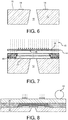
- the flow feature layer 40 is then exposed to UV radiation 42 through a mask 44 having an opaque area 46 and a transparent area 48 as described above and as shown in FIG. 7 .
- the flow feature layer 40 is heated to cross-link the UV exposed areas of the flow feature layer 40 under the transparent areas 48 of the mask 44.
- the flow feature layer 40 is not developed at this stage of the process.
- the nozzle plate layer 50 is laminated to the exposed and undeveloped flow feature layer 40 using a compression roll laminator 52. Adhesion may be promoted between the flow feature layer 40 and the nozzle plate layer 50 by treating the flow feature layer 40 with oxygen plasma and a forming gas and/or silane. Since the undeveloped flow feature layer 40 provides support for the nozzle plate layer 50, more aggressive temperatures and pressures may be used to laminate the nozzle plate layer 50 to the flow feature layer 40.
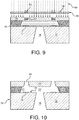
- the nozzle plate layer 50 is exposed to UV radiation 54 through a mask 56, having transparent areas 58 and opaque areas 60 corresponding to nozzle hole areas 62 ( FIG. 9 ). After exposing the nozzle plate layer 50 to UV radiation 54, the nozzle plate layer 50 and the flow feature layer 40 are developed simultaneously using a photoresist developer ( FIG. 10 ).
- the substrate 12 containing the exposed flow feature layer 40 and the exposed nozzle plate layer 50 is placed in a developer bath using mega-sonic agitation to dissolve the uncross-linked materials in both the flow feature layer 40 and nozzle plate layer 50, so that the uncrosslinked material from the flow feature layer 40 is dissolved through the previously formed fluid supply via 18 and the uncrosslinked material from the nozzle plate layer 50 is dissolved through nozzle holes 64 in the nozzle plate layer 50.
- Illustrative developers used in the developer bath include, for example, butyl cellosolve acetate, cyclohexanone, methyl ethyl ketone, a xylene and butyl cellosolve acetate mixture, and C 1-6 acetates like butyl acetate, or a combination of two or more of the foregoing.
- the nozzle plate layer 50 is a single layer of photoresist material.
- the nozzle plate layer 50 includes: a hydrophilic photoresist material layer disposed adjacent to the flow feature layer 40; and a hydrophobic photoresist material layer disposed adjacent to the hydrophilic photoresist material layer.
- the hydrophilic photoresist material layer may have a water contact angle ranging from about 60 degrees to about 90 degrees, such as from about 80 degrees to about 88 degrees.
- the hydrophobic photoresist material layer may have a water contact angle ranging from about 91 degrees to about 120 degrees.
- a phenoxy resin may be added to the hydrophobic photoresist material layer to increase the hydrophilicity of hydrophilic photoresist material layer.
- Compounds that may be added to the hydrophobic photoresist material layer to increase the hydrophobicity of hydrophobic photoresist material layer may include, but are not limited to heptadecafluorodecyltrimethoxysilane, octadecyldimethylchlorosilane, octadecyltricholorsilane, and siloxanes.
- the nozzle holes 64 typically have an inlet diameter ranging from about 10 microns to about 50 microns, and an outlet diameter ranging from about 6 microns to about 40 microns. Due to the size of the nozzle holes 64, even slight variations or imperfections may have a tremendous impact on the performance of the fluid ejection head 70.
- a feature of the embodiment of FIGs. 6-10 is improved alignment tolerances between nozzle holes 64 in the nozzle plate layer 50 and the heater resistors 14, since the nozzle holes 64 are formed in the nozzle plate layer 50 after the nozzle plate layer 50 is attached to the flow feature layer 40. Imaging the nozzle holes 64 after attaching a nozzle plate layer 50 to the flow feature layer 40 enables placement of the nozzle holes 64 in the optimum location for each of the heater resistor 14.
- Another benefit of the disclosed embodiments is that the DRIE process used to form the fluid supply vias 18 will not harm the flow feature layer 40 since the fluid supply vias 18 are formed prior to applying the flow feature layer 40 to the substrate 12.
- a further benefit of the disclosed embodiments is that more complex processing of fluidic devices may be achieved using thicker flow feature layers than can be achieved with the prior art process.
- the embodiments provide for simpler process steps and a reduction in the number of process steps required to make a fluid ejection head 70.
Landscapes
- Engineering & Computer Science (AREA)
- Manufacturing & Machinery (AREA)
- Particle Formation And Scattering Control In Inkjet Printers (AREA)
Abstract
Description
- The disclosure relates to fluid ejection devices, and in particular to improved methods for making fluid ejection head structures.
- Fluid ejection heads are useful for ejecting a variety of fluids including inks, cooling fluids, pharmaceuticals, lubricants and the like. A widely used fluid ejection head is in an inkjet printer. However, fluid ejection heads may also be used in vaporization devices for vapor therapy, E-cigarettes and the like. New techniques are constantly being developed to provide low cost, highly reliable fluid ejection heads for such devices.
- The fluid ejection head is a seemingly simple device that has a relatively complicated structure containing electrical circuits, ink passageways and a variety of tiny parts assembled with precision to provide a powerful, yet versatile fluid ejection head. The components of the ejection head must cooperate with each other and be useful for a variety of fluids and fluid formulations. Accordingly, it is important to match the ejection head components to the fluid being ejected. Slight variations in production quality can have a tremendous influence on the product yield and resulting ejection head performance.
- The primary components of a fluid ejection head are a semiconductor substrate, a flow feature layer, a nozzle plate layer, and a flexible circuit attached to the substrate. The semiconductor substrate is preferably made of silicon and contains various passivation layers, conductive metal layers, resistive layers, insulative layers and protective layers deposited on a device surface thereof. Fluid ejection actuators formed on a device surface of the substrate may be thermal actuators or piezoelectric actuators. For thermal actuators, individual heater resistors are defined in the resistive layers and each heater resistor corresponds to a nozzle hole in the nozzle plate for heating and ejecting fluid from the ejection head toward a desired substrate or target.
- The nozzle plate layer and the flow feature layer may each be made of a photo-imageable material. The flow feature layer is typically spin-coated onto the substrate, imaged and developed to provide flow features therein for directing fluid from a fluid via in the substrate to a heater on the substrate. Next, the substrate is etched to form the fluid vias in a deep reactive ion etching (DRIE) process. A dry film photoresist nozzle layer is then laminated to the flow feature layer using heated, pressure rollers. Finally, the nozzle layer is exposed and developed to form the nozzle holes therein.
- During the nozzle plate layer lamination process, the nozzle plate layer is bridged across the fluid via in the substrate and the flow features in the flow feature layer. Stresses are introduced from the laminator rollers into the nozzle plate layer as the laminator roll radially compresses the nozzle plate layer, pushing the nozzle plate layer down into unsupported regions of the flow feature layer. The radial compression of the nozzle plate layer causes UV light diffraction during nozzle plate layer imaging, resulting in poor nozzle hole image quality. A second factor contributing to poor nozzle hole image quality is the fact that the heaters on the substrate are constructed of highly reflective material. The highly reflective material causes UV light rays used during nozzle plate imaging to reflect back into the nozzle plate layer photoresist material causing areas of the unexposed nozzle holes to be exposed to small amounts of UV radiation that results in misshapen nozzle holes.
- The planarity of the nozzle plate layer is critical to controlling fluid ejection directionality. Nozzle hole diameter variances also may cause drop mass inconsistencies. Accordingly, there continues to be a need for manufacturing processes and techniques which provide improved fluid ejection head components.
- In view of the foregoing, embodiments of the disclosure provide improved fluid ejection heads and a method for making fluid ejection heads. The method of making a fluid ejection head includes steps of: providing a substrate, being configured to contain a plurality fluid ejection actuators on a device surface thereof; forming one or more fluid supply vias in the substrate; laminating a first photoresist layer to a device surface of the substrate; exposing the first photoresist layer to a first ultraviolet (UV) radiation through a first photo mask to provide a first UV exposed area of the first photoresist layer; heating the first photoresist layer to cross-link material in the first UV exposed area of the first photoresist layer; laminating a second photoresist layer to the first photoresist layer; exposing the second photoresist layer to a second UV radiation through a second photo mask to provide a second UV exposed area for nozzle holes; cross-linking the second photoresist layer with heat; and developing the first photoresist layer and second photoresist layer to form flow features in the first photoresist layer and nozzle holes in the second photoresist layers.
- In another embodiment, there is provided a fluid ejection head. The fluid ejection head includes a substrate configured to contain a plurality of fluid ejection actuators on a device surface thereof and one or more fluid supply vias formed therethrough; a first photoresist layer, configured to be laminated to the device surface of the substrate; and a second photoresist layer, configured to be laminated to the first photoresist layer. The second photoresist layer includes: a hydrophilic photoresist material layer disposed adjacent to the first photoresist layer; and a hydrophobic photoresist material layer disposed adjacent to the hydrophilic photoresist material layer.
- In one embodiment, the first photoresist layer is configured to provide an anti-reflective coating on the substrate. In another embodiment, the first photoresist layer is configured to have a thickness ranging from about 10 µm to about 30 µm.
- In another embodiment, the second photoresist layer is configured to have a thickness ranging from about 10 µm to about 30.
- In one embodiment, the hydrophilic photoresist material layer is configured to have a water contact angle ranging from about 60 degrees to less than about 90 degrees. In another embodiment, the hydrophobic photoresist material layer is configured to have a water contact angle ranging from about 91 degrees to about 120 degrees.
- In one embodiment, the device surface of the substrate is configured to be plasma treated for promoting adhesion between the first photoresist layer and the device surface of the substrate. In another embodiment, the first photoresist layer is configured to be plasma treated with oxygen and a forming gas to promote adhesion between the first photoresist layer and the second photoresist layer.
- In one embodiment, the fluid ejection head is an inkjet print head.
- An advantage of the embodiments described herein is that the first photoresist layer, or flow feature layer, is effective to minimize stresses on the second photoresist layer, or nozzle plate layer, during a lamination process for the second photoresist layer. Another advantage of the disclosed embodiments, is that the first photoresist layer may be used as an anti-reflective layer between the second photoresist layer and highly reflective heater surfaces during an imaging step for the second photoresist layer. Yet another advantage of the disclosed embodiments is that a reactive ion etching process for fluid supply vias in the substrate is conducted before the first photoresist layer is applied to the substrate thereby avoiding flow feature damage during the etching or striping processes, which would enable more aggressive strip processes for higher fluid ejection head yields.
- Further features and advantages of the disclosed embodiments will become apparent by reference to the detailed description when considered in conjunction with the figures, which are not to scale, wherein like reference numbers indicate like elements through the several views, and wherein:
-
FIG. 1A is a schematic cross-sectional view, not to scale, of a portion of a fluid ejection head according to the disclosure. -
FIG. 1B is a plan schematic view seen along 1B-1B line inFIG. 1A , not to scale, of a portion of a fluid ejection head according to the disclosure. -
FIGs. 2-5A are schematic views, not to scale, of prior art steps for making a fluid ejection head. -
FIG. 5B is a schematic perspective view, not to scale, of a nozzle plate layer resulting from the process shown inFIGs. 2-5A . -
FIGs. 6-10 are schematic views, not to scale, of steps for making a fluid ejection head according to the disclosure. - With reference to
FIGs. 1A and 1B , there is shown a simplified representation of a portion of a prior artfluid ejection head 10. Thefluid ejection head 10 includes asubstrate 12 that is preferably a silicon semiconductor substrate containing a plurality of fluid ejection actuators such as piezoelectric devices orheater resistors 14 formed on adevice surface 16 of thesubstrate 12, as shown in the simplified illustration ofFIG. 1A . Upon activation ofheater resistors 14, fluid supplied through one or morefluid supply vias 18 in thesubstrate 12 flows through afluid supply channel 20 to afluid chamber 22 in athick film layer 24 where the fluid is caused to be ejected throughnozzle holes 26 in anozzle plate layer 28. Fluid ejection actuators, such asheater resistors 14, are formed on thedevice surface 16 of thesubstrate 12 by well-known semiconductor manufacturing techniques. - The
substrate 12 is relatively small in size and typically has overall dimensions ranging from about 2 millimeters to about 8 millimeters wide by about 10 millimeters to about 20 millimeters long, and from about 0.4 mm to about 0.8 mm thick. Thefluid supply vias 18 are grit-blasted in thesubstrates 12. Suchfluid supply vias 18 typically have dimensions of about 9.7 millimeters long and from about 50 microns to about 400 microns wide. Fluid may be provided to the fluid ejection actuators by a single one of the fluid supply via 18 or by a plurality of openings in thesubstrate 12 made by a dry etch process selected from reactive ion etching (RIE) or deep reactive ion etching (DRIE), inductively coupled plasma etching, and the like. - The fluid supply via 18 directs fluid from a fluid reservoir to which the
fluid ejection head 10 is attached through the fluid supply via 18 to thedevice surface 16 of thesubstrate 12 containingheater resistors 14. Thedevice surface 16 of thesubstrate 12 also preferably contains electrical tracing from theheater resistors 14 to contact pads used for connecting thesubstrate 12 to a flexible circuit or a tape automated bonding (TAB) circuit for supplying electrical impulses from a fluid ejection controller to activate one ormore heater resistors 14 on thesubstrate 12. - A prior art process for making a
fluid ejection head 10 is illustrated schematically inFIGs. 2-6 . According to the prior art process, thethick film layer 24 is spin-coated onto thedevice surface 16 of thesubstrate 12 containing theheater resistors 14. Thethick film layer 24 may be formed from a negative photoresist material. Thethick film layer 24 may have a thickness ranging from about 10 µm to about 80 µm or more, such as from about 20 µm to about 60 µm. - After coating the substrate, the
thick film layer 24 is heated to remove solvents from the spin coated material leaving a solid layer of photoresist material on thesubstrate 12. A mask 30 (FIG. 3 ) is used to mask off those areas of thethick film layer 24 that are to remain soluble. Accordingly, themask 30 contains substantially transparent areas 32 and substantiallyopaque areas 34 for imaging thethick film layer 24. Ultraviolet (UV)radiation 36 is used to image thethick film layer 24 and cross-link the negative photoresist material. - After imaging the
thick film layer 24, thesubstrate 12 andthick film layer 24 are further heated to cross-link the photoresist material in the exposed areas thereof. A developer solvent is then applied to thesubstrate 12 andthick film layer 24 to remove uncured photoresist material thereby forming thefluid supply channels 20 andfluid chambers 22 therein. A third heating step at a temperature of about 200 °C for about 2 hours may be used to remove any residual photo-initiator that may be in the photoresist material. - Next, the
substrate 12 containing the imaged and developedthick film layer 24 is etched using a deep reactive ion etching (DRIE) process to form the fluid supply via 18 therein. The DRIE process typically uses a positive photoresist material to mask thesubstrate 12. The positive photoresist material is removed after etching thesubstrate 12 using a high-pressure solvent strip process.FIG. 4 shows thesubstrate 12 andthick film layer 24 after etching the fluid supply via 18 through thesubstrate 12. - In the next step of the process, a dry-film negative photoresist material used to provide the
nozzle plate layer 28 is laminated to thethick film layer 24 using aheated roll laminator 38 as shown inFIG. 5A . Thenozzle plate layer 28 has a thickness ranging from about 5 µm to about 50 µm, such as from about 10 µm to about 30 µm. During the lamination process, thenozzle plate layer 28 bridges across the fluid supply via 18 and flow features of thethick film layer 24 and the rolls of theroll laminator 38 compress thenozzle plate layer 28 radially pushing it down into the unsupported fluid supply via 18,fluid supply channel 20 andfluid chamber 22. The compression of thenozzle plate layer 28 may cause UV light diffraction during the imaging step for thenozzle plate layer 28 thereby causingpoor nozzle hole 26 quality as shown inFIG. 5B . A second factor that may contribute topoor nozzle hole 26 image quality is the fact that theheater resistors 14 on thesubstrate 12 are made of highly reflective metal. The highly reflective metal causes the UV radiation to reflect back into thenozzle plate layer 28, causing areas of theunexposed nozzle hole 26 to be exposed to a small amount of unwanted UV radiation resulting in themisshapen nozzle hole 26 illustrated inFIG. 5B . - The planarity of the
nozzle plate layer 28 is critical to controlling fluid ejection directionality. Also nozzle diameter variances may also cause drop mass inconsistencies. Accordingly, an improved process for making a fluid ejection head is provided according to the disclosure. - According to an embodiment of the disclosure, a
flow feature layer 40 is used to support a nozzle plate layer and provide an anti-reflective coating over the highlyreflective heater resistors 14 on thesubstrate 12. Suchflow feature layer 40 may be a photoresist material having an index of refraction, when measured at the wavelengths of UV radiation used for imaging the nozzle holes, that is lower than an index of refraction of a nozzle plate layer. In another embodiment, theflow feature layer 40 may be selected from material that absorbs UV radiation at the wavelengths used for imaging the nozzle holes in a nozzle plate layer. In other embodiments, theflow feature layer 40 may be a material that absorbs UV radiation and that has an index of refraction that is lower than the index of refraction of a nozzle plate layer. Such removable and/or patternableflow feature layer 40 may be selected from a negative photoresist material containing UV absorbent fillers, such as dyes or pigments. - Such dye or pigment filled photoresist layer may be patterned using UV radiation so that it remains in the
fluid supply channels 20 andfluid chambers 22 over theheater resistors 14 and/or electrical contacts on thedevice surface 16 of thesubstrate 12. During the formation of the nozzle holes, UV radiation used to form the nozzle holes is absorbed by theflow feature layer 40, so that no significant amount of 365 nanometer radiation is reflected off thedevice surface 16 of thesubstrate 12 thereby preventing irregular nozzle hole formation. - A process for using the
flow feature layer 40 to provide support is illustrated inFIGs. 6-10 . Prior to depositing theflow feature layer 40 and thenozzle plate layer 50 on thesubstrate 12, thesubstrate 12 is etched using a deep reactive ion etching (DRIE) process to form thefluid supply vias 18 therein. The DRIE process is as described above. The positive photoresist material is removed after etching thesubstrate 12 using a high pressure solvent strip process.FIG. 6 shows thesubstrate 12 after etching the fluid supply via 18 through thesubstrate 12. - Next a
flow feature layer 40 is applied to thesubstrate 12 by dry laminating theflow feature layer 40 onto thedevice surface 16 of thesubstrate 12. Thedevice surface 16 of thesubstrate 12 may be prepared to promote adhesion between thesubstrate 12 and theflow feature layer 40 by plasma treating thedevice surface 16 with oxygen and/or silane before laminating theflow feature layer 40 to thesubstrate 12. Silane compounds that are compatible with the components of the photoresist formulation typically have a functional group capable of reacting with at least one member selected from the group consisting of a multifunctional epoxy compound, a difunctional epoxy compound and a photo-initiator. Such an adhesion enhancing agent may be a silane with an epoxide functional group such as a glycidoxy-alkyltrialkoxysilane, e.g., gamma-glycidoxypropyltrimethoxysilane. When used, the adhesion enhancing agent is preferably present in an amount ranging from about 0.5 to about 2 weight percent and more preferably from about 1.0 to about 1.5 weight percent based on total weight of the cured resin, including all ranges subsumed therein. Adhesion enhancing agents, as used herein, are defined to mean organic materials soluble in the photoresist composition which assist the film forming and adhesion characteristics of theflow feature layer 40 on thedevice surface 16 of thesubstrate 12. - The
flow feature layer 40 is then exposed toUV radiation 42 through amask 44 having anopaque area 46 and atransparent area 48 as described above and as shown inFIG. 7 . Theflow feature layer 40 is heated to cross-link the UV exposed areas of theflow feature layer 40 under thetransparent areas 48 of themask 44. However, unlike the prior art process, theflow feature layer 40 is not developed at this stage of the process. - In the next step of the process, as shown in
FIG. 8 , thenozzle plate layer 50 is laminated to the exposed and undevelopedflow feature layer 40 using acompression roll laminator 52. Adhesion may be promoted between theflow feature layer 40 and thenozzle plate layer 50 by treating theflow feature layer 40 with oxygen plasma and a forming gas and/or silane. Since the undevelopedflow feature layer 40 provides support for thenozzle plate layer 50, more aggressive temperatures and pressures may be used to laminate thenozzle plate layer 50 to theflow feature layer 40. - In order to provide
nozzle holes 64 in thenozzle plate layer 50, thenozzle plate layer 50 is exposed toUV radiation 54 through amask 56, having transparent areas 58 and opaque areas 60 corresponding to nozzle hole areas 62 (FIG. 9 ). After exposing thenozzle plate layer 50 toUV radiation 54, thenozzle plate layer 50 and theflow feature layer 40 are developed simultaneously using a photoresist developer (FIG. 10 ). In one embodiment, thesubstrate 12 containing the exposedflow feature layer 40 and the exposednozzle plate layer 50 is placed in a developer bath using mega-sonic agitation to dissolve the uncross-linked materials in both theflow feature layer 40 andnozzle plate layer 50, so that the uncrosslinked material from theflow feature layer 40 is dissolved through the previously formed fluid supply via 18 and the uncrosslinked material from thenozzle plate layer 50 is dissolved through nozzle holes 64 in thenozzle plate layer 50. Illustrative developers used in the developer bath include, for example, butyl cellosolve acetate, cyclohexanone, methyl ethyl ketone, a xylene and butyl cellosolve acetate mixture, and C1-6 acetates like butyl acetate, or a combination of two or more of the foregoing. - In some embodiments, the
nozzle plate layer 50 is a single layer of photoresist material. In other embodiments, thenozzle plate layer 50 includes: a hydrophilic photoresist material layer disposed adjacent to theflow feature layer 40; and a hydrophobic photoresist material layer disposed adjacent to the hydrophilic photoresist material layer. The hydrophilic photoresist material layer may have a water contact angle ranging from about 60 degrees to about 90 degrees, such as from about 80 degrees to about 88 degrees. And, the hydrophobic photoresist material layer may have a water contact angle ranging from about 91 degrees to about 120 degrees. A phenoxy resin may be added to the hydrophobic photoresist material layer to increase the hydrophilicity of hydrophilic photoresist material layer. Compounds that may be added to the hydrophobic photoresist material layer to increase the hydrophobicity of hydrophobic photoresist material layer may include, but are not limited to heptadecafluorodecyltrimethoxysilane, octadecyldimethylchlorosilane, octadecyltricholorsilane, and siloxanes. - The nozzle holes 64 typically have an inlet diameter ranging from about 10 microns to about 50 microns, and an outlet diameter ranging from about 6 microns to about 40 microns. Due to the size of the nozzle holes 64, even slight variations or imperfections may have a tremendous impact on the performance of the
fluid ejection head 70. - A feature of the embodiment of
FIGs. 6-10 is improved alignment tolerances between nozzle holes 64 in thenozzle plate layer 50 and theheater resistors 14, since the nozzle holes 64 are formed in thenozzle plate layer 50 after thenozzle plate layer 50 is attached to theflow feature layer 40. Imaging the nozzle holes 64 after attaching anozzle plate layer 50 to theflow feature layer 40 enables placement of the nozzle holes 64 in the optimum location for each of theheater resistor 14. - Another benefit of the disclosed embodiments is that the DRIE process used to form the
fluid supply vias 18 will not harm theflow feature layer 40 since thefluid supply vias 18 are formed prior to applying theflow feature layer 40 to thesubstrate 12. - A further benefit of the disclosed embodiments is that more complex processing of fluidic devices may be achieved using thicker flow feature layers than can be achieved with the prior art process.
- Finally, the embodiments provide for simpler process steps and a reduction in the number of process steps required to make a
fluid ejection head 70. -
- 10 :
- fluid ejection head
- 12 :
- substrate
- 14 :
- heater resistor
- 16 :
- device surface
- 18 :
- fluid supply via
- 20 :
- fluid supply channel
- 22 :
- fluid chamber
- 24 :
- thick film layer
- 26 :
- nozzle hole
- 28 :
- nozzle plate layer
- 30 :
- mask
- 32 :
- transparent area
- 34 :
- opaque area
- 36 :
- ultraviolet radiation
- 38 :
- roll laminator
- 40 :
- flow feature layer
- 42 :
- ultraviolet radiation
- 44 :
- mask
- 46 :
- opaque area
- 48 :
- transparent area
- 50 :
- nozzle plate layer
- 52 :
- compression roll laminator
- 54 :
- ultraviolet radiation
- 56 :
- mask
- 58 :
- transparent area
- 60 :
- opaque area
- 62 :
- nozzle hole area
- 64 :
- nozzle hole
- 70 :
- fluid ejection head
Claims (14)
- A fluid ejection head (70), comprising:a substrate (12), configured to contain a plurality of fluid ejection actuators (14) on a device surface (16) thereof and one or more fluid supply vias (18) formed therethrough;a first photoresist layer (40), configured to be laminated to the device surface (16) of the substrate (12); anda second photoresist layer (50), configured to be laminated to the first photoresist layer (40),wherein the second photoresist layer (50) comprises:a hydrophilic photoresist material layer disposed adjacent to the first photoresist layer (40), anda hydrophobic photoresist material layer disposed adjacent to the hydrophilic photoresist material layer.
- The fluid ejection head (70) of claim 1, wherein
the first photoresist layer (40) is configured to provide an anti-reflective coating on the substrate (12). - The fluid ejection head (70) of claim 1 or claim 2, wherein
the first photoresist layer (40) is configured to have a thickness ranging from about 10 µm to about 30 µm. - The fluid ejection head (70) of any one of claim 1 to claim 3, wherein
the second photoresist layer (50) is configured to have a thickness ranging from about 10µm to about 30 µm. - The fluid ejection head (70) of any one of claim 1 to claim 4, wherein
the hydrophilic photoresist material layer is configured to have a water contact angle ranging from about 60 degrees to less than about 90 degrees. - The fluid ejection head (70) of any one of claim 1 to claim 5, wherein
the hydrophobic photoresist material layer is configured to have a water contact angle ranging from about 91 degrees to about 120 degrees. - A method of making a fluid ejection head (70), comprising:providing a substrate (12), being configured to contain a plurality of fluid ejection actuators (14) on a device surface (16) thereof;forming one or more fluid supply vias (18) in the substrate (12);laminating a first photoresist layer (40) to the device surface (16) of the substrate (12);exposing the first photoresist layer (40) to a first ultraviolet radiation (42) through a first photo mask (44) to provide a first ultraviolet exposed area of the first photoresist layer (40);heating the first photoresist layer (40) to cross-link a material in the first ultraviolet exposed area of the first photoresist layer (40);laminating a second photoresist layer (50) to the first photoresist layer (40);exposing the second photoresist layer (50) to a second ultraviolet radiation (54) through a second photo mask (56) to provide a second ultraviolet exposed area (62) for nozzle holes (64);cross-linking the second photoresist layer (50) with heat; anddeveloping the first photoresist layer (40) and the second photoresist layer (50) to form flow features in the first photoresist layer (40) and nozzle holes (64) in the second photoresist layer (50).
- The method of claim 7, wherein
the first photoresist layer (40) is configured to provide an anti-reflective coating on the substrate. - The method of claim 7 or claim 8, wherein
the first photoresist layer (40) is configured to be laminated to the substrate (12) with a thickness ranging from about 10 µm to about 30 µm. - The method of any one of claim 7 to claim 9, wherein
the second photoresist layer (50) is configured to be laminated to the first photoresist layer (40) with a thickness ranging from about 10 µm to about 30 µm. - The method of any one of claim 7 to claim 10, wherein
the first photoresist layer (40) is configured to comprise a hydrophilic photoresist material. - The method of any one of claim 7 to claim 11, wherein
the second photoresist layer (50) comprises:a hydrophilic photoresist material layer disposed adjacent to the first photoresist layer (40), anda hydrophobic photoresist material layer disposed adjacent to the hydrophilic photoresist material layer. - The method of any one of claim 7 to claim 12, wherein
the device surface (16) of the substrate (12) is configured to be plasma treated for promoting adhesion between the first photoresist layer (40) and the device surface (16) of the substrate (12). - The method of any one of claim 7 to claim 13, wherein
the first photoresist layer (40) is configured to be plasma treated with oxygen and a forming gas to promote adhesion between the first photoresist layer (40) and the second photoresist layer (50).
Applications Claiming Priority (1)
| Application Number | Priority Date | Filing Date | Title |
|---|---|---|---|
| US15/295,335 US9855566B1 (en) | 2016-10-17 | 2016-10-17 | Fluid ejection head and process for making a fluid ejection head structure |
Publications (2)
| Publication Number | Publication Date |
|---|---|
| EP3312011A1 true EP3312011A1 (en) | 2018-04-25 |
| EP3312011B1 EP3312011B1 (en) | 2021-01-13 |
Family
ID=60043069
Family Applications (1)
| Application Number | Title | Priority Date | Filing Date |
|---|---|---|---|
| EP17195399.5A Active EP3312011B1 (en) | 2016-10-17 | 2017-10-09 | Fluid ejection head and method for making fluid ejection head |
Country Status (4)
| Country | Link |
|---|---|
| US (1) | US9855566B1 (en) |
| EP (1) | EP3312011B1 (en) |
| JP (1) | JP7003556B2 (en) |
| CN (1) | CN107953672B (en) |
Cited By (2)
| Publication number | Priority date | Publication date | Assignee | Title |
|---|---|---|---|---|
| EP3447578A1 (en) * | 2017-08-21 | 2019-02-27 | Funai Electric Co., Ltd. | Three-dimensional structure, method for making three-dimensional structure, and fluid ejection device |
| EP4060406A3 (en) * | 2021-03-19 | 2022-10-26 | Funai Electric Co., Ltd. | Composite photoresist material and method for making thereof, and fluid ejection head |
Families Citing this family (10)
| Publication number | Priority date | Publication date | Assignee | Title |
|---|---|---|---|---|
| WO2021021136A1 (en) * | 2019-07-30 | 2021-02-04 | Hewlett-Packard Development Company L.P. | Uniform print head surface coating |
| US11666918B2 (en) * | 2020-03-06 | 2023-06-06 | Funai Electric Co., Ltd. | Microfluidic chip, head, and dispensing device for dispensing fluids containing an acidic component |
| WO2021211094A1 (en) | 2020-04-14 | 2021-10-21 | Hewlett-Packard Development Company, L.P. | Fluid-ejection die with stamped nanoceramic layer |
| US11577513B2 (en) * | 2020-10-06 | 2023-02-14 | Funai Electric Co., Ltd. | Photoimageable nozzle member for reduced fluid cross-contamination and method therefor |
| US11926157B2 (en) * | 2021-03-05 | 2024-03-12 | Funai Electric Co., Ltd. | Photoresist imaging and development for enhanced nozzle plate adhesion |
| US11896971B2 (en) | 2021-03-18 | 2024-02-13 | Punai Electric Co., Ltd. | Fluid detection circuit for fluid ejection head |
| JP7651909B2 (en) * | 2021-03-31 | 2025-03-27 | セイコーエプソン株式会社 | Liquid injection nozzle and liquid injection device |
| US20220323973A1 (en) * | 2021-04-08 | 2022-10-13 | Funai Electric Co., Ltd. | Modified fluid jet plume characteristics |
| US11642886B2 (en) * | 2021-04-08 | 2023-05-09 | Funai Electric Co., Ltd. | Modified fluid jet plume characteristics |
| US12600130B2 (en) | 2023-08-22 | 2026-04-14 | Brady Worldwide, Inc. | Ejection head nozzle flooding control |
Citations (13)
| Publication number | Priority date | Publication date | Assignee | Title |
|---|---|---|---|---|
| US6409312B1 (en) * | 2001-03-27 | 2002-06-25 | Lexmark International, Inc. | Ink jet printer nozzle plate and process therefor |
| US20060057503A1 (en) * | 2004-09-10 | 2006-03-16 | Bertelsen Craig M | Process for making a micro-fluid ejection head structure |
| US20070070122A1 (en) * | 2005-09-23 | 2007-03-29 | Lexmark International, Inc | Methods for making micro-fluid ejection head structures |
| US20080313900A1 (en) * | 2007-06-21 | 2008-12-25 | Samsung Electronics Co., Ltd. | Method of manufacturing inkjet print head |
| US20090191488A1 (en) * | 2008-01-25 | 2009-07-30 | Canon Kabushiki Kaisha | Ink jet recording head and manufacturing method |
| JP2012030458A (en) * | 2010-07-30 | 2012-02-16 | Brother Industries Ltd | Method of manufacturing ink ejection head |
| US20130002753A1 (en) * | 2011-06-28 | 2013-01-03 | Yongcai Wang | Microfluidic device having improved epoxy layer adhesion |
| US20130048601A1 (en) * | 2011-08-31 | 2013-02-28 | Paul Dryer | Use of Hydrogen-Oxygen Plasma for Forming Hydroxyl Functional Groups on a Polymer Surface |
| US20140068940A1 (en) * | 2012-09-11 | 2014-03-13 | Canon Kabushiki Kaisha | Process for producing liquid ejection head |
| US20140083974A1 (en) * | 2012-09-21 | 2014-03-27 | Canon Kabushiki Kaisha | Process for producing liquid ejection head |
| US20140311661A1 (en) * | 2013-04-23 | 2014-10-23 | Canon Kabushiki Kaisha | Process for producing a liquid ejection head |
| US20160052270A1 (en) * | 2014-08-20 | 2016-02-25 | Canon Kabushiki Kaisha | Inkjet recording head and method of manufacturing the same |
| US20160271949A1 (en) * | 2015-03-20 | 2016-09-22 | Canon Kabushiki Kaisha | Process for producing liquid discharge head |
Family Cites Families (22)
| Publication number | Priority date | Publication date | Assignee | Title |
|---|---|---|---|---|
| JPH04185347A (en) * | 1990-11-16 | 1992-07-02 | Ricoh Co Ltd | Droplet flight recording device |
| JP2727988B2 (en) * | 1994-12-15 | 1998-03-18 | 日本電気株式会社 | Method of manufacturing ink jet print head |
| JPH08295018A (en) * | 1995-04-26 | 1996-11-12 | Matsushita Electric Ind Co Ltd | Inkjet head |
| WO1999015337A1 (en) * | 1997-09-22 | 1999-04-01 | Cimeo Precision Co., Ltd. | Ink-jet head nozzle plate, its manufacturing method and ink-jet head |
| JP2003300323A (en) | 2002-04-11 | 2003-10-21 | Canon Inc | Ink jet head and method of manufacturing the same |
| KR100534616B1 (en) | 2004-05-03 | 2005-12-07 | 삼성전자주식회사 | method of hydrophobicity treatment of nozzle plate for use in ink jet head |
| US7198353B2 (en) * | 2004-06-30 | 2007-04-03 | Lexmark International, Inc. | Integrated black and colored ink printheads |
| KR100765315B1 (en) | 2004-07-23 | 2007-10-09 | 삼성전자주식회사 | An inkjet head having a filtering member integrally formed with a substrate, and a method of manufacturing the same. |
| KR100641357B1 (en) | 2004-08-26 | 2006-11-01 | 삼성전자주식회사 | Inkjet Printheads and Manufacturing Method Thereof |
| JP2006130766A (en) * | 2004-11-05 | 2006-05-25 | Canon Inc | Substrate for liquid discharge head and manufacturing method thereof |
| US7479203B2 (en) | 2005-08-22 | 2009-01-20 | Lexmark International, Inc. | Lamination of dry film to micro-fluid ejection head substrates |
| JP2007245640A (en) | 2006-03-17 | 2007-09-27 | Canon Inc | Inkjet recording head |
| KR20080102903A (en) * | 2007-05-22 | 2008-11-26 | 삼성전자주식회사 | Manufacturing method of inkjet printer head and inkjet printer head manufactured by said method |
| KR100906804B1 (en) * | 2007-09-27 | 2009-07-09 | 삼성전기주식회사 | Nozzle Plates, Inkjet Heads and Their Manufacturing Methods |
| JP2009178906A (en) | 2008-01-30 | 2009-08-13 | Canon Inc | Method for manufacturing ink jet recording head |
| US8173030B2 (en) | 2008-09-30 | 2012-05-08 | Eastman Kodak Company | Liquid drop ejector having self-aligned hole |
| JP5538844B2 (en) * | 2008-12-19 | 2014-07-02 | キヤノン株式会社 | Method for manufacturing liquid discharge head |
| JP5693204B2 (en) | 2010-12-17 | 2015-04-01 | キヤノン株式会社 | Method for manufacturing ink jet recording head |
| JP6039259B2 (en) * | 2011-07-25 | 2016-12-07 | キヤノン株式会社 | Liquid discharge head and manufacturing method thereof |
| JP5828702B2 (en) | 2011-07-26 | 2015-12-09 | キヤノン株式会社 | Method for manufacturing liquid discharge head |
| JP2014136402A (en) * | 2013-01-18 | 2014-07-28 | Canon Inc | Method for forming fine structure and method for manufacturing ink jet head |
| JP6395518B2 (en) * | 2014-09-01 | 2018-09-26 | キヤノン株式会社 | Method for manufacturing liquid discharge head |
-
2016
- 2016-10-17 US US15/295,335 patent/US9855566B1/en active Active
-
2017
- 2017-10-09 EP EP17195399.5A patent/EP3312011B1/en active Active
- 2017-10-11 CN CN201710945916.8A patent/CN107953672B/en active Active
- 2017-10-12 JP JP2017198274A patent/JP7003556B2/en active Active
Patent Citations (13)
| Publication number | Priority date | Publication date | Assignee | Title |
|---|---|---|---|---|
| US6409312B1 (en) * | 2001-03-27 | 2002-06-25 | Lexmark International, Inc. | Ink jet printer nozzle plate and process therefor |
| US20060057503A1 (en) * | 2004-09-10 | 2006-03-16 | Bertelsen Craig M | Process for making a micro-fluid ejection head structure |
| US20070070122A1 (en) * | 2005-09-23 | 2007-03-29 | Lexmark International, Inc | Methods for making micro-fluid ejection head structures |
| US20080313900A1 (en) * | 2007-06-21 | 2008-12-25 | Samsung Electronics Co., Ltd. | Method of manufacturing inkjet print head |
| US20090191488A1 (en) * | 2008-01-25 | 2009-07-30 | Canon Kabushiki Kaisha | Ink jet recording head and manufacturing method |
| JP2012030458A (en) * | 2010-07-30 | 2012-02-16 | Brother Industries Ltd | Method of manufacturing ink ejection head |
| US20130002753A1 (en) * | 2011-06-28 | 2013-01-03 | Yongcai Wang | Microfluidic device having improved epoxy layer adhesion |
| US20130048601A1 (en) * | 2011-08-31 | 2013-02-28 | Paul Dryer | Use of Hydrogen-Oxygen Plasma for Forming Hydroxyl Functional Groups on a Polymer Surface |
| US20140068940A1 (en) * | 2012-09-11 | 2014-03-13 | Canon Kabushiki Kaisha | Process for producing liquid ejection head |
| US20140083974A1 (en) * | 2012-09-21 | 2014-03-27 | Canon Kabushiki Kaisha | Process for producing liquid ejection head |
| US20140311661A1 (en) * | 2013-04-23 | 2014-10-23 | Canon Kabushiki Kaisha | Process for producing a liquid ejection head |
| US20160052270A1 (en) * | 2014-08-20 | 2016-02-25 | Canon Kabushiki Kaisha | Inkjet recording head and method of manufacturing the same |
| US20160271949A1 (en) * | 2015-03-20 | 2016-09-22 | Canon Kabushiki Kaisha | Process for producing liquid discharge head |
Cited By (2)
| Publication number | Priority date | Publication date | Assignee | Title |
|---|---|---|---|---|
| EP3447578A1 (en) * | 2017-08-21 | 2019-02-27 | Funai Electric Co., Ltd. | Three-dimensional structure, method for making three-dimensional structure, and fluid ejection device |
| EP4060406A3 (en) * | 2021-03-19 | 2022-10-26 | Funai Electric Co., Ltd. | Composite photoresist material and method for making thereof, and fluid ejection head |
Also Published As
| Publication number | Publication date |
|---|---|
| CN107953672B (en) | 2019-12-24 |
| JP7003556B2 (en) | 2022-01-20 |
| US9855566B1 (en) | 2018-01-02 |
| EP3312011B1 (en) | 2021-01-13 |
| JP2018065381A (en) | 2018-04-26 |
| CN107953672A (en) | 2018-04-24 |
Similar Documents
| Publication | Publication Date | Title |
|---|---|---|
| EP3312011B1 (en) | Fluid ejection head and method for making fluid ejection head | |
| US6409312B1 (en) | Ink jet printer nozzle plate and process therefor | |
| CA1169472A (en) | Ink jet head | |
| US7275817B2 (en) | Formation of novel ink jet filter printhead using transferable photopatterned filter layer | |
| US5686224A (en) | Ink jet print head having channel structures integrally formed therein | |
| JPH0558898B2 (en) | ||
| US9873255B2 (en) | Liquid ejection head and method of manufacturing the same | |
| JPH0415095B2 (en) | ||
| JP2003145780A (en) | Method of manufacturing ink jet print head | |
| US8273524B2 (en) | Liquid discharging head, producing method thereof, structure, and producing method thereof | |
| JPS5919168A (en) | Ink jet recording head | |
| EP3446877B1 (en) | Three-dimensional structure, method for making three-dimensional structure, and fluid ejection device | |
| EP3447579A1 (en) | Three-dimensional structure, method for making three-dimendional structure, and fluid ejection device | |
| US10279589B2 (en) | Method for manufacturing structure | |
| KR101520622B1 (en) | Ink-jet printhead and manufacturing method thereof | |
| US20050167043A1 (en) | Formation of photopatterned ink jet nozzle modules using photopatternable nozzle-forming bonding layer | |
| JP7134831B2 (en) | Manufacturing method of liquid ejection head | |
| EP3447578A1 (en) | Three-dimensional structure, method for making three-dimensional structure, and fluid ejection device | |
| US8241540B2 (en) | Method of manufacturing liquid discharge head | |
| EP4052914A1 (en) | Fluid ejection head, method for improving the same and method for making fluid jet ejection head | |
| JPH0712662B2 (en) | Method for manufacturing ink jet recording head | |
| US10744771B2 (en) | Method of manufacturing liquid ejection head and method of manufacturing structure | |
| JPS58224758A (en) | inkjet recording head | |
| JPS591268A (en) | Manufacture of ink jet recording head | |
| JPH0592563A (en) | Ink jet head and method of manufacturing the same |
Legal Events
| Date | Code | Title | Description |
|---|---|---|---|
| PUAI | Public reference made under article 153(3) epc to a published international application that has entered the european phase |
Free format text: ORIGINAL CODE: 0009012 |
|
| STAA | Information on the status of an ep patent application or granted ep patent |
Free format text: STATUS: THE APPLICATION HAS BEEN PUBLISHED |
|
| AK | Designated contracting states |
Kind code of ref document: A1 Designated state(s): AL AT BE BG CH CY CZ DE DK EE ES FI FR GB GR HR HU IE IS IT LI LT LU LV MC MK MT NL NO PL PT RO RS SE SI SK SM TR |
|
| AX | Request for extension of the european patent |
Extension state: BA ME |
|
| STAA | Information on the status of an ep patent application or granted ep patent |
Free format text: STATUS: REQUEST FOR EXAMINATION WAS MADE |
|
| 17P | Request for examination filed |
Effective date: 20181017 |
|
| RBV | Designated contracting states (corrected) |
Designated state(s): AL AT BE BG CH CY CZ DE DK EE ES FI FR GB GR HR HU IE IS IT LI LT LU LV MC MK MT NL NO PL PT RO RS SE SI SK SM TR |
|
| GRAP | Despatch of communication of intention to grant a patent |
Free format text: ORIGINAL CODE: EPIDOSNIGR1 |
|
| STAA | Information on the status of an ep patent application or granted ep patent |
Free format text: STATUS: GRANT OF PATENT IS INTENDED |
|
| INTG | Intention to grant announced |
Effective date: 20200918 |
|
| RIN1 | Information on inventor provided before grant (corrected) |
Inventor name: WEAVER, SEAN T. Inventor name: BERNARD, DAVID L. Inventor name: MCNEES, ANDREW L. Inventor name: CRAFT, CHRISTOPHER A. |
|
| GRAS | Grant fee paid |
Free format text: ORIGINAL CODE: EPIDOSNIGR3 |
|
| GRAA | (expected) grant |
Free format text: ORIGINAL CODE: 0009210 |
|
| STAA | Information on the status of an ep patent application or granted ep patent |
Free format text: STATUS: THE PATENT HAS BEEN GRANTED |
|
| AK | Designated contracting states |
Kind code of ref document: B1 Designated state(s): AL AT BE BG CH CY CZ DE DK EE ES FI FR GB GR HR HU IE IS IT LI LT LU LV MC MK MT NL NO PL PT RO RS SE SI SK SM TR |
|
| REG | Reference to a national code |
Ref country code: GB Ref legal event code: FG4D |
|
| REG | Reference to a national code |
Ref country code: CH Ref legal event code: EP |
|
| REG | Reference to a national code |
Ref country code: DE Ref legal event code: R096 Ref document number: 602017031298 Country of ref document: DE |
|
| REG | Reference to a national code |
Ref country code: IE Ref legal event code: FG4D |
|
| REG | Reference to a national code |
Ref country code: AT Ref legal event code: REF Ref document number: 1354261 Country of ref document: AT Kind code of ref document: T Effective date: 20210215 |
|
| REG | Reference to a national code |
Ref country code: AT Ref legal event code: MK05 Ref document number: 1354261 Country of ref document: AT Kind code of ref document: T Effective date: 20210113 |
|
| REG | Reference to a national code |
Ref country code: NL Ref legal event code: MP Effective date: 20210113 |
|
| REG | Reference to a national code |
Ref country code: LT Ref legal event code: MG9D |
|
| PG25 | Lapsed in a contracting state [announced via postgrant information from national office to epo] |
Ref country code: FI Free format text: LAPSE BECAUSE OF FAILURE TO SUBMIT A TRANSLATION OF THE DESCRIPTION OR TO PAY THE FEE WITHIN THE PRESCRIBED TIME-LIMIT Effective date: 20210113 Ref country code: HR Free format text: LAPSE BECAUSE OF FAILURE TO SUBMIT A TRANSLATION OF THE DESCRIPTION OR TO PAY THE FEE WITHIN THE PRESCRIBED TIME-LIMIT Effective date: 20210113 Ref country code: GR Free format text: LAPSE BECAUSE OF FAILURE TO SUBMIT A TRANSLATION OF THE DESCRIPTION OR TO PAY THE FEE WITHIN THE PRESCRIBED TIME-LIMIT Effective date: 20210414 Ref country code: PT Free format text: LAPSE BECAUSE OF FAILURE TO SUBMIT A TRANSLATION OF THE DESCRIPTION OR TO PAY THE FEE WITHIN THE PRESCRIBED TIME-LIMIT Effective date: 20210513 Ref country code: NO Free format text: LAPSE BECAUSE OF FAILURE TO SUBMIT A TRANSLATION OF THE DESCRIPTION OR TO PAY THE FEE WITHIN THE PRESCRIBED TIME-LIMIT Effective date: 20210413 Ref country code: BG Free format text: LAPSE BECAUSE OF FAILURE TO SUBMIT A TRANSLATION OF THE DESCRIPTION OR TO PAY THE FEE WITHIN THE PRESCRIBED TIME-LIMIT Effective date: 20210413 Ref country code: LT Free format text: LAPSE BECAUSE OF FAILURE TO SUBMIT A TRANSLATION OF THE DESCRIPTION OR TO PAY THE FEE WITHIN THE PRESCRIBED TIME-LIMIT Effective date: 20210113 |
|
| PG25 | Lapsed in a contracting state [announced via postgrant information from national office to epo] |
Ref country code: SE Free format text: LAPSE BECAUSE OF FAILURE TO SUBMIT A TRANSLATION OF THE DESCRIPTION OR TO PAY THE FEE WITHIN THE PRESCRIBED TIME-LIMIT Effective date: 20210113 Ref country code: AT Free format text: LAPSE BECAUSE OF FAILURE TO SUBMIT A TRANSLATION OF THE DESCRIPTION OR TO PAY THE FEE WITHIN THE PRESCRIBED TIME-LIMIT Effective date: 20210113 Ref country code: LV Free format text: LAPSE BECAUSE OF FAILURE TO SUBMIT A TRANSLATION OF THE DESCRIPTION OR TO PAY THE FEE WITHIN THE PRESCRIBED TIME-LIMIT Effective date: 20210113 Ref country code: PL Free format text: LAPSE BECAUSE OF FAILURE TO SUBMIT A TRANSLATION OF THE DESCRIPTION OR TO PAY THE FEE WITHIN THE PRESCRIBED TIME-LIMIT Effective date: 20210113 Ref country code: RS Free format text: LAPSE BECAUSE OF FAILURE TO SUBMIT A TRANSLATION OF THE DESCRIPTION OR TO PAY THE FEE WITHIN THE PRESCRIBED TIME-LIMIT Effective date: 20210113 |
|
| PG25 | Lapsed in a contracting state [announced via postgrant information from national office to epo] |
Ref country code: IS Free format text: LAPSE BECAUSE OF FAILURE TO SUBMIT A TRANSLATION OF THE DESCRIPTION OR TO PAY THE FEE WITHIN THE PRESCRIBED TIME-LIMIT Effective date: 20210513 |
|
| REG | Reference to a national code |
Ref country code: DE Ref legal event code: R097 Ref document number: 602017031298 Country of ref document: DE |
|
| PG25 | Lapsed in a contracting state [announced via postgrant information from national office to epo] |
Ref country code: EE Free format text: LAPSE BECAUSE OF FAILURE TO SUBMIT A TRANSLATION OF THE DESCRIPTION OR TO PAY THE FEE WITHIN THE PRESCRIBED TIME-LIMIT Effective date: 20210113 Ref country code: CZ Free format text: LAPSE BECAUSE OF FAILURE TO SUBMIT A TRANSLATION OF THE DESCRIPTION OR TO PAY THE FEE WITHIN THE PRESCRIBED TIME-LIMIT Effective date: 20210113 Ref country code: SM Free format text: LAPSE BECAUSE OF FAILURE TO SUBMIT A TRANSLATION OF THE DESCRIPTION OR TO PAY THE FEE WITHIN THE PRESCRIBED TIME-LIMIT Effective date: 20210113 |
|
| PLBE | No opposition filed within time limit |
Free format text: ORIGINAL CODE: 0009261 |
|
| STAA | Information on the status of an ep patent application or granted ep patent |
Free format text: STATUS: NO OPPOSITION FILED WITHIN TIME LIMIT |
|
| PG25 | Lapsed in a contracting state [announced via postgrant information from national office to epo] |
Ref country code: DK Free format text: LAPSE BECAUSE OF FAILURE TO SUBMIT A TRANSLATION OF THE DESCRIPTION OR TO PAY THE FEE WITHIN THE PRESCRIBED TIME-LIMIT Effective date: 20210113 Ref country code: RO Free format text: LAPSE BECAUSE OF FAILURE TO SUBMIT A TRANSLATION OF THE DESCRIPTION OR TO PAY THE FEE WITHIN THE PRESCRIBED TIME-LIMIT Effective date: 20210113 Ref country code: SK Free format text: LAPSE BECAUSE OF FAILURE TO SUBMIT A TRANSLATION OF THE DESCRIPTION OR TO PAY THE FEE WITHIN THE PRESCRIBED TIME-LIMIT Effective date: 20210113 |
|
| 26N | No opposition filed |
Effective date: 20211014 |
|
| PG25 | Lapsed in a contracting state [announced via postgrant information from national office to epo] |
Ref country code: AL Free format text: LAPSE BECAUSE OF FAILURE TO SUBMIT A TRANSLATION OF THE DESCRIPTION OR TO PAY THE FEE WITHIN THE PRESCRIBED TIME-LIMIT Effective date: 20210113 Ref country code: ES Free format text: LAPSE BECAUSE OF FAILURE TO SUBMIT A TRANSLATION OF THE DESCRIPTION OR TO PAY THE FEE WITHIN THE PRESCRIBED TIME-LIMIT Effective date: 20210113 |
|
| PG25 | Lapsed in a contracting state [announced via postgrant information from national office to epo] |
Ref country code: SI Free format text: LAPSE BECAUSE OF FAILURE TO SUBMIT A TRANSLATION OF THE DESCRIPTION OR TO PAY THE FEE WITHIN THE PRESCRIBED TIME-LIMIT Effective date: 20210113 |
|
| PG25 | Lapsed in a contracting state [announced via postgrant information from national office to epo] |
Ref country code: IT Free format text: LAPSE BECAUSE OF FAILURE TO SUBMIT A TRANSLATION OF THE DESCRIPTION OR TO PAY THE FEE WITHIN THE PRESCRIBED TIME-LIMIT Effective date: 20210113 |
|
| REG | Reference to a national code |
Ref country code: CH Ref legal event code: PL |
|
| PG25 | Lapsed in a contracting state [announced via postgrant information from national office to epo] |
Ref country code: IS Free format text: LAPSE BECAUSE OF FAILURE TO SUBMIT A TRANSLATION OF THE DESCRIPTION OR TO PAY THE FEE WITHIN THE PRESCRIBED TIME-LIMIT Effective date: 20210513 |
|
| REG | Reference to a national code |
Ref country code: BE Ref legal event code: MM Effective date: 20211031 |
|
| GBPC | Gb: european patent ceased through non-payment of renewal fee |
Effective date: 20211009 |
|
| PG25 | Lapsed in a contracting state [announced via postgrant information from national office to epo] |
Ref country code: MC Free format text: LAPSE BECAUSE OF FAILURE TO SUBMIT A TRANSLATION OF THE DESCRIPTION OR TO PAY THE FEE WITHIN THE PRESCRIBED TIME-LIMIT Effective date: 20210113 |
|
| PG25 | Lapsed in a contracting state [announced via postgrant information from national office to epo] |
Ref country code: LU Free format text: LAPSE BECAUSE OF NON-PAYMENT OF DUE FEES Effective date: 20211009 Ref country code: GB Free format text: LAPSE BECAUSE OF NON-PAYMENT OF DUE FEES Effective date: 20211009 Ref country code: BE Free format text: LAPSE BECAUSE OF NON-PAYMENT OF DUE FEES Effective date: 20211031 |
|
| PG25 | Lapsed in a contracting state [announced via postgrant information from national office to epo] |
Ref country code: LI Free format text: LAPSE BECAUSE OF NON-PAYMENT OF DUE FEES Effective date: 20211031 Ref country code: CH Free format text: LAPSE BECAUSE OF NON-PAYMENT OF DUE FEES Effective date: 20211031 |
|
| PG25 | Lapsed in a contracting state [announced via postgrant information from national office to epo] |
Ref country code: FR Free format text: LAPSE BECAUSE OF NON-PAYMENT OF DUE FEES Effective date: 20211031 |
|
| PG25 | Lapsed in a contracting state [announced via postgrant information from national office to epo] |
Ref country code: IE Free format text: LAPSE BECAUSE OF NON-PAYMENT OF DUE FEES Effective date: 20211009 |
|
| PG25 | Lapsed in a contracting state [announced via postgrant information from national office to epo] |
Ref country code: HU Free format text: LAPSE BECAUSE OF FAILURE TO SUBMIT A TRANSLATION OF THE DESCRIPTION OR TO PAY THE FEE WITHIN THE PRESCRIBED TIME-LIMIT; INVALID AB INITIO Effective date: 20171009 |
|
| PG25 | Lapsed in a contracting state [announced via postgrant information from national office to epo] |
Ref country code: NL Free format text: LAPSE BECAUSE OF NON-PAYMENT OF DUE FEES Effective date: 20210113 Ref country code: CY Free format text: LAPSE BECAUSE OF FAILURE TO SUBMIT A TRANSLATION OF THE DESCRIPTION OR TO PAY THE FEE WITHIN THE PRESCRIBED TIME-LIMIT Effective date: 20210113 |
|
| PG25 | Lapsed in a contracting state [announced via postgrant information from national office to epo] |
Ref country code: MK Free format text: LAPSE BECAUSE OF FAILURE TO SUBMIT A TRANSLATION OF THE DESCRIPTION OR TO PAY THE FEE WITHIN THE PRESCRIBED TIME-LIMIT Effective date: 20210113 |
|
| PG25 | Lapsed in a contracting state [announced via postgrant information from national office to epo] |
Ref country code: MT Free format text: LAPSE BECAUSE OF FAILURE TO SUBMIT A TRANSLATION OF THE DESCRIPTION OR TO PAY THE FEE WITHIN THE PRESCRIBED TIME-LIMIT Effective date: 20210113 |
|
| REG | Reference to a national code |
Ref country code: DE Ref legal event code: R081 Ref document number: 602017031298 Country of ref document: DE Owner name: BRADY WORLDWIDE, INC., MILWAUKEE, US Free format text: FORMER OWNER: FUNAI ELECTRIC CO., LTD., DAITO-SHI, OSAKA, JP Ref country code: DE Ref legal event code: R082 Ref document number: 602017031298 Country of ref document: DE Representative=s name: BOULT WADE TENNANT LLP, DE |
|
| PG25 | Lapsed in a contracting state [announced via postgrant information from national office to epo] |
Ref country code: TR Free format text: LAPSE BECAUSE OF FAILURE TO SUBMIT A TRANSLATION OF THE DESCRIPTION OR TO PAY THE FEE WITHIN THE PRESCRIBED TIME-LIMIT Effective date: 20210113 |
|
| PGFP | Annual fee paid to national office [announced via postgrant information from national office to epo] |
Ref country code: DE Payment date: 20251229 Year of fee payment: 9 |