EP3310136B1 - Composition for moisture permeation preventing film for electronic device, method for forming moisture permeation preventing film for electronic device using same, and electronic device - Google Patents
Composition for moisture permeation preventing film for electronic device, method for forming moisture permeation preventing film for electronic device using same, and electronic device Download PDFInfo
- Publication number
- EP3310136B1 EP3310136B1 EP15895025.3A EP15895025A EP3310136B1 EP 3310136 B1 EP3310136 B1 EP 3310136B1 EP 15895025 A EP15895025 A EP 15895025A EP 3310136 B1 EP3310136 B1 EP 3310136B1
- Authority
- EP
- European Patent Office
- Prior art keywords
- electronic device
- moisture permeation
- preventing film
- permeation preventing
- composition
- Prior art date
- Legal status (The legal status is an assumption and is not a legal conclusion. Google has not performed a legal analysis and makes no representation as to the accuracy of the status listed.)
- Active
Links
Images




Classifications
-
- C—CHEMISTRY; METALLURGY
- C08—ORGANIC MACROMOLECULAR COMPOUNDS; THEIR PREPARATION OR CHEMICAL WORKING-UP; COMPOSITIONS BASED THEREON
- C08K—Use of inorganic or non-macromolecular organic substances as compounding ingredients
- C08K3/00—Use of inorganic substances as compounding ingredients
- C08K3/34—Silicon-containing compounds
- C08K3/36—Silica
-
- B—PERFORMING OPERATIONS; TRANSPORTING
- B32—LAYERED PRODUCTS
- B32B—LAYERED PRODUCTS, i.e. PRODUCTS BUILT-UP OF STRATA OF FLAT OR NON-FLAT, e.g. CELLULAR OR HONEYCOMB, FORM
- B32B27/00—Layered products comprising a layer of synthetic resin
- B32B27/06—Layered products comprising a layer of synthetic resin as the main or only constituent of a layer, which is next to another layer of the same or of a different material
-
- C—CHEMISTRY; METALLURGY
- C03—GLASS; MINERAL OR SLAG WOOL
- C03C—CHEMICAL COMPOSITION OF GLASSES, GLAZES OR VITREOUS ENAMELS; SURFACE TREATMENT OF GLASS; SURFACE TREATMENT OF FIBRES OR FILAMENTS MADE FROM GLASS, MINERALS OR SLAGS; JOINING GLASS TO GLASS OR OTHER MATERIALS
- C03C17/00—Surface treatment of glass, not in the form of fibres or filaments, by coating
- C03C17/006—Surface treatment of glass, not in the form of fibres or filaments, by coating with materials of composite character
- C03C17/007—Surface treatment of glass, not in the form of fibres or filaments, by coating with materials of composite character containing a dispersed phase, e.g. particles, fibres or flakes, in a continuous phase
-
- C—CHEMISTRY; METALLURGY
- C08—ORGANIC MACROMOLECULAR COMPOUNDS; THEIR PREPARATION OR CHEMICAL WORKING-UP; COMPOSITIONS BASED THEREON
- C08J—WORKING-UP; GENERAL PROCESSES OF COMPOUNDING; AFTER-TREATMENT NOT COVERED BY SUBCLASSES C08B, C08C, C08F, C08G or C08H
- C08J5/00—Manufacture of articles or shaped materials containing macromolecular substances
- C08J5/18—Manufacture of films or sheets
-
- C—CHEMISTRY; METALLURGY
- C08—ORGANIC MACROMOLECULAR COMPOUNDS; THEIR PREPARATION OR CHEMICAL WORKING-UP; COMPOSITIONS BASED THEREON
- C08J—WORKING-UP; GENERAL PROCESSES OF COMPOUNDING; AFTER-TREATMENT NOT COVERED BY SUBCLASSES C08B, C08C, C08F, C08G or C08H
- C08J7/00—Chemical treatment or coating of shaped articles made of macromolecular substances
- C08J7/04—Coating
- C08J7/0427—Coating with only one layer of a composition containing a polymer binder
-
- C—CHEMISTRY; METALLURGY
- C08—ORGANIC MACROMOLECULAR COMPOUNDS; THEIR PREPARATION OR CHEMICAL WORKING-UP; COMPOSITIONS BASED THEREON
- C08J—WORKING-UP; GENERAL PROCESSES OF COMPOUNDING; AFTER-TREATMENT NOT COVERED BY SUBCLASSES C08B, C08C, C08F, C08G or C08H
- C08J7/00—Chemical treatment or coating of shaped articles made of macromolecular substances
- C08J7/04—Coating
- C08J7/043—Improving the adhesiveness of the coatings per se, e.g. forming primers
-
- C—CHEMISTRY; METALLURGY
- C09—DYES; PAINTS; POLISHES; NATURAL RESINS; ADHESIVES; COMPOSITIONS NOT OTHERWISE PROVIDED FOR; APPLICATIONS OF MATERIALS NOT OTHERWISE PROVIDED FOR
- C09D—COATING COMPOSITIONS, e.g. PAINTS, VARNISHES OR LACQUERS; FILLING PASTES; CHEMICAL PAINT OR INK REMOVERS; INKS; CORRECTING FLUIDS; WOODSTAINS; PASTES OR SOLIDS FOR COLOURING OR PRINTING; USE OF MATERIALS THEREFOR
- C09D7/00—Features of coating compositions, not provided for in group C09D5/00; Processes for incorporating ingredients in coating compositions
- C09D7/40—Additives
- C09D7/60—Additives non-macromolecular
- C09D7/61—Additives non-macromolecular inorganic
-
- H—ELECTRICITY
- H05—ELECTRIC TECHNIQUES NOT OTHERWISE PROVIDED FOR
- H05K—PRINTED CIRCUITS; CASINGS OR CONSTRUCTIONAL DETAILS OF ELECTRIC APPARATUS; MANUFACTURE OF ASSEMBLAGES OF ELECTRICAL COMPONENTS
- H05K3/00—Apparatus or processes for manufacturing printed circuits
- H05K3/22—Secondary treatment of printed circuits
- H05K3/28—Applying non-metallic protective coatings
-
- B—PERFORMING OPERATIONS; TRANSPORTING
- B32—LAYERED PRODUCTS
- B32B—LAYERED PRODUCTS, i.e. PRODUCTS BUILT-UP OF STRATA OF FLAT OR NON-FLAT, e.g. CELLULAR OR HONEYCOMB, FORM
- B32B2309/00—Parameters for the laminating or treatment process; Apparatus details
- B32B2309/08—Dimensions, e.g. volume
- B32B2309/10—Dimensions, e.g. volume linear, e.g. length, distance, width
- B32B2309/105—Thickness
-
- B—PERFORMING OPERATIONS; TRANSPORTING
- B32—LAYERED PRODUCTS
- B32B—LAYERED PRODUCTS, i.e. PRODUCTS BUILT-UP OF STRATA OF FLAT OR NON-FLAT, e.g. CELLULAR OR HONEYCOMB, FORM
- B32B2457/00—Electrical equipment
- B32B2457/20—Displays, e.g. liquid crystal displays, plasma displays
-
- C—CHEMISTRY; METALLURGY
- C03—GLASS; MINERAL OR SLAG WOOL
- C03C—CHEMICAL COMPOSITION OF GLASSES, GLAZES OR VITREOUS ENAMELS; SURFACE TREATMENT OF GLASS; SURFACE TREATMENT OF FIBRES OR FILAMENTS MADE FROM GLASS, MINERALS OR SLAGS; JOINING GLASS TO GLASS OR OTHER MATERIALS
- C03C2217/00—Coatings on glass
- C03C2217/40—Coatings comprising at least one inhomogeneous layer
- C03C2217/43—Coatings comprising at least one inhomogeneous layer consisting of a dispersed phase in a continuous phase
- C03C2217/46—Coatings comprising at least one inhomogeneous layer consisting of a dispersed phase in a continuous phase characterized by the dispersed phase
- C03C2217/47—Coatings comprising at least one inhomogeneous layer consisting of a dispersed phase in a continuous phase characterized by the dispersed phase consisting of a specific material
- C03C2217/475—Inorganic materials
- C03C2217/478—Silica
-
- C—CHEMISTRY; METALLURGY
- C03—GLASS; MINERAL OR SLAG WOOL
- C03C—CHEMICAL COMPOSITION OF GLASSES, GLAZES OR VITREOUS ENAMELS; SURFACE TREATMENT OF GLASS; SURFACE TREATMENT OF FIBRES OR FILAMENTS MADE FROM GLASS, MINERALS OR SLAGS; JOINING GLASS TO GLASS OR OTHER MATERIALS
- C03C2217/00—Coatings on glass
- C03C2217/70—Properties of coatings
- C03C2217/76—Hydrophobic and oleophobic coatings
-
- C—CHEMISTRY; METALLURGY
- C08—ORGANIC MACROMOLECULAR COMPOUNDS; THEIR PREPARATION OR CHEMICAL WORKING-UP; COMPOSITIONS BASED THEREON
- C08J—WORKING-UP; GENERAL PROCESSES OF COMPOUNDING; AFTER-TREATMENT NOT COVERED BY SUBCLASSES C08B, C08C, C08F, C08G or C08H
- C08J2333/00—Characterised by the use of homopolymers or copolymers of compounds having one or more unsaturated aliphatic radicals, each having only one carbon-to-carbon double bond, and only one being terminated by only one carboxyl radical, or of salts, anhydrides, esters, amides, imides, or nitriles thereof; Derivatives of such polymers
- C08J2333/04—Characterised by the use of homopolymers or copolymers of compounds having one or more unsaturated aliphatic radicals, each having only one carbon-to-carbon double bond, and only one being terminated by only one carboxyl radical, or of salts, anhydrides, esters, amides, imides, or nitriles thereof; Derivatives of such polymers esters
-
- C—CHEMISTRY; METALLURGY
- C08—ORGANIC MACROMOLECULAR COMPOUNDS; THEIR PREPARATION OR CHEMICAL WORKING-UP; COMPOSITIONS BASED THEREON
- C08J—WORKING-UP; GENERAL PROCESSES OF COMPOUNDING; AFTER-TREATMENT NOT COVERED BY SUBCLASSES C08B, C08C, C08F, C08G or C08H
- C08J2367/00—Characterised by the use of polyesters obtained by reactions forming a carboxylic ester link in the main chain; Derivatives of such polymers
- C08J2367/02—Polyesters derived from dicarboxylic acids and dihydroxy compounds
-
- C—CHEMISTRY; METALLURGY
- C08—ORGANIC MACROMOLECULAR COMPOUNDS; THEIR PREPARATION OR CHEMICAL WORKING-UP; COMPOSITIONS BASED THEREON
- C08J—WORKING-UP; GENERAL PROCESSES OF COMPOUNDING; AFTER-TREATMENT NOT COVERED BY SUBCLASSES C08B, C08C, C08F, C08G or C08H
- C08J2369/00—Characterised by the use of polycarbonates; Derivatives of polycarbonates
-
- C—CHEMISTRY; METALLURGY
- C08—ORGANIC MACROMOLECULAR COMPOUNDS; THEIR PREPARATION OR CHEMICAL WORKING-UP; COMPOSITIONS BASED THEREON
- C08J—WORKING-UP; GENERAL PROCESSES OF COMPOUNDING; AFTER-TREATMENT NOT COVERED BY SUBCLASSES C08B, C08C, C08F, C08G or C08H
- C08J2379/00—Characterised by the use of macromolecular compounds obtained by reactions forming in the main chain of the macromolecule a linkage containing nitrogen with or without oxygen, or carbon only, not provided for in groups C08J2361/00 - C08J2377/00
- C08J2379/04—Polycondensates having nitrogen-containing heterocyclic rings in the main chain; Polyhydrazides; Polyamide acids or similar polyimide precursors
- C08J2379/08—Polyimides; Polyester-imides; Polyamide-imides; Polyamide acids or similar polyimide precursors
-
- C—CHEMISTRY; METALLURGY
- C08—ORGANIC MACROMOLECULAR COMPOUNDS; THEIR PREPARATION OR CHEMICAL WORKING-UP; COMPOSITIONS BASED THEREON
- C08J—WORKING-UP; GENERAL PROCESSES OF COMPOUNDING; AFTER-TREATMENT NOT COVERED BY SUBCLASSES C08B, C08C, C08F, C08G or C08H
- C08J2381/00—Characterised by the use of macromolecular compounds obtained by reactions forming in the main chain of the macromolecule a linkage containing sulfur with or without nitrogen, oxygen, or carbon only; Polysulfones; Derivatives of such polymers
- C08J2381/06—Polysulfones; Polyethersulfones
-
- C—CHEMISTRY; METALLURGY
- C08—ORGANIC MACROMOLECULAR COMPOUNDS; THEIR PREPARATION OR CHEMICAL WORKING-UP; COMPOSITIONS BASED THEREON
- C08J—WORKING-UP; GENERAL PROCESSES OF COMPOUNDING; AFTER-TREATMENT NOT COVERED BY SUBCLASSES C08B, C08C, C08F, C08G or C08H
- C08J2383/00—Characterised by the use of macromolecular compounds obtained by reactions forming in the main chain of the macromolecule a linkage containing silicon with or without sulfur, nitrogen, oxygen, or carbon only; Derivatives of such polymers
- C08J2383/04—Polysiloxanes
-
- C—CHEMISTRY; METALLURGY
- C08—ORGANIC MACROMOLECULAR COMPOUNDS; THEIR PREPARATION OR CHEMICAL WORKING-UP; COMPOSITIONS BASED THEREON
- C08J—WORKING-UP; GENERAL PROCESSES OF COMPOUNDING; AFTER-TREATMENT NOT COVERED BY SUBCLASSES C08B, C08C, C08F, C08G or C08H
- C08J2483/00—Characterised by the use of macromolecular compounds obtained by reactions forming in the main chain of the macromolecule a linkage containing silicon with or without sulfur, nitrogen, oxygen, or carbon only; Derivatives of such polymers
- C08J2483/04—Polysiloxanes
-
- C—CHEMISTRY; METALLURGY
- C08—ORGANIC MACROMOLECULAR COMPOUNDS; THEIR PREPARATION OR CHEMICAL WORKING-UP; COMPOSITIONS BASED THEREON
- C08K—Use of inorganic or non-macromolecular organic substances as compounding ingredients
- C08K7/00—Use of ingredients characterised by shape
- C08K7/22—Expanded, porous or hollow particles
- C08K7/24—Expanded, porous or hollow particles inorganic
- C08K7/26—Silicon- containing compounds
-
- H—ELECTRICITY
- H05—ELECTRIC TECHNIQUES NOT OTHERWISE PROVIDED FOR
- H05K—PRINTED CIRCUITS; CASINGS OR CONSTRUCTIONAL DETAILS OF ELECTRIC APPARATUS; MANUFACTURE OF ASSEMBLAGES OF ELECTRICAL COMPONENTS
- H05K3/00—Apparatus or processes for manufacturing printed circuits
- H05K3/22—Secondary treatment of printed circuits
- H05K3/28—Applying non-metallic protective coatings
- H05K3/285—Permanent coating compositions
Definitions
- the present invention relates to a composition for a moisture permeation preventing film for an electronic device, a method for forming a moisture permeation preventing film for an electronic device using the same, and an electronic device.
- glass materials are mainly used as the material for a moisture permeation preventing film for an electronic device when flexibility is not required, and when flexibility is required, film or ink materials are used.
- moisture permeation preventing films are generally formed in a multilayer structure in order to secure low moisture permeability which is the unique function of a moisture permeation preventing film for an electronic device.
- WO2005/047746 describes a curable coating composition for forming a thermal insulating layer.
- JP2000043179 describes a humidity controlling layer containing mesoporous silica on a plastic sheet.
- KR101288736 relates to an aerogel paste and a manufacturing method of the same are provided to coat the surfaces of various materials including films.
- the present inventors attempt to solve the problems described above by disclosing a composition for a moisture permeation preventing film for an electronic device including an aerogel.
- a method for forming a moisture permeation preventing film for an electronic device in a simple process using the composition is disclosed, and in addition, an electronic device including the moisture permeation preventing film is disclosed.
- composition for a moisture permeation preventing film for an electronic device comprising:
- the solvent may be at least one selected from the group consisting of toluene, ethyl alcohol, methyl ethyl ketone (MEK), n-heptane, and isopropyl alcohol (IPA).
- the additive may be a surfactant, an antifoaming agent, or a mixture thereof.
- the surfactant may be at least one selected from the group consisting of sodium alkyl diphenyloxide disulfonate, polyoxyethylene tridecyl ether sulfate, polyalkyleneoxide silane, sodium alkyl diphenyloxide disulfonate, and a fluoric surfactant.
- the antifoaming agent may be at least one selected from the group consisting of silicone, polysiloxane, polymethylsiloxane, modified polysiloxane, and ether-modified polysiloxane.
- a method for forming a moisture permeation preventing film for an electronic device comprising a step of preparing a composition for a moisture permeation preventing film for an electronic device, comprising 1 to 10 wt% of an aerogel that comprises silica, 10 to 50 wt% of a solvent, 0.1 to 5 wt% of an additive that is a surfactant, an antifoaming agent, or a mixture thereof, and a binder as the remainder, the binder comprising silicone oil or at least one selected from the group consisting of a silanol group, an alkoxysilyl group, and polydimethylsiloxane, in a molecule; a step of applying the composition for a moisture permeation preventing film for an electronic device on a substrate; and a step of drying the applied composition for a moisture permeation preventing film for an electronic device on the substrate.
- an application amount of the composition for a moisture permeation preventing film for an electronic device per area (m 2 ) of each side of the substrate may be 135 to 1,227 g/m 2 .
- an electronic device including a substrate; and a moisture permeation preventing film for an electronic device, located on the substrate and including 1 to 10 wt% of an aerogel that comprises silica, 0.1 to 5 wt% of an additive that is a surfactant, an antifoaming agent, or a mixture thereof, and a binder as the remainder, the binder comprising silicone oil or at least one selected from the group consisting of a silanol group, an alkoxysilyl group, and polydimethylsiloxane, in a molecule.
- the moisture permeation preventing film for an electronic device is described as follows.
- the moisture permeation preventing film for an electronic device may have a thickness in a range of 100 to 900 ⁇ m.
- the moisture permeation preventing film for an electronic device may be formed as a single layer.
- the substrate is described as follows.
- the substrate may be a flexible board.
- the flexible board may consist of a material selected from the group consisting of polyethylene terephthalate (PET), polyacrylate (PA), polycarbonate (PC), polyethersulfone (PES), polyimide (PI), and a combination thereof.
- PET polyethylene terephthalate
- PA polyacrylate
- PC polycarbonate
- PES polyethersulfone
- PI polyimide
- the substrate may be a rigid board.
- the rigid board may consist of a material selected from glass.
- the electronic device may be a touch panel, a battery, or a display device.
- a composition for a moisture permeation preventing film for an electronic device which is capable of lowering moisture permeability by including an aerogel, thereby preventing deterioration of the function of the electronic device, and prolonging the lifespan thereof, a method for forming a moisture permeation preventing film using the same, and an electronic device can be provided.
- the moisture permeation preventing film can be applied in various electronic devices such as touch panel sensors, batteries, and the like.
- the invention provides a composition for a moisture permeation preventing film for an electronic device.
- composition for a moisture permeation preventing film for an electronic device which, by including an aerogel (specifically, hydrophobic aerogel), is capable of lowering moisture permeability by including an aerogel, thereby preventing deterioration of the function of an electronic device and prolonging the lifespan thereof.
- an aerogel specifically, hydrophobic aerogel
- moisture permeation preventing film can be secured, applications for flexible and/or wearable display devices are possible, and the moisture permeation preventing film can be advantageously applied in various electronic devices such as touch panel sensors, batteries, and the like.
- the composition for a moisture permeation preventing film for an electronic device includes 1 to 10 wt% of an aerogel; 10 to 50 wt% of a solvent; 0.1 to 5 wt% of an additive; and a binder as the remainder based on a total 100 wt% of the composition for a moisture permeation preventing film for an electronic device, and the reason for limiting the content of each material thereto is described as follows.
- Aerogel 1 to 10 wt%
- the viscosity of the composition becomes too high, and as a result, it is difficult to uniformly form a moisture permeation preventing film. Accordingly, a phenomenon in which the transparency and permeability of the formed moisture permeation preventing film are reduced may occur. On the contrary, at below 1 wt%, the content of the aerogel is too low to be expected to be effective.
- the content of the solvent in the composition for a moisture permeation preventing film for an electronic device satisfying a range of 10 to 50 wt% can result in the viscosity and density in which the binder, the aerogel, and the additive can be properly dispersed.
- the density of the composition decreases, which is a factor for increased moisture permeability of the moisture permeation preventing film thus formed.
- the viscosity of the composition becomes too high, and as a result, it is difficult for each material to be uniformly dispersed, and the moisture permeation preventing film thus formed may contain bubbles which are difficult to be removed.
- the composition for a moisture permeation preventing film for an electronic device may include the additive at 0.1 wt% to 5 wt% therein.
- the content of the aerogel relatively decreases, and as a result, the moisture permeability of the moisture permeation preventing film thus formed may decrease.
- a hydrophobic aerogel may contribute to significantly lowering the moisture permeability of a moisture permeation preventing film.
- the aerogel includes silica, and in the examples described below, such silica aerogel is used.
- the particle diameter of the aerogel is not particularly limited, it is necessary for the diameter to be less than or equal to the thickness of the moisture permeation preventing film to be formed.
- the binder is described as follows.
- the binder may include silicone oil.
- the binder may include at least one selected from the group consisting of a silanol group, an alkoxysilyl group, and polydimethylsiloxane, in a molecule.
- the solvent as previously described, is not particularly limited as long as the solvent is a material capable of dissolving and uniformly dispersing the aerogel, the binder, and the additive.
- the solvent may be at least one selected from the group consisting of toluene, ethyl alcohol, methyl ethyl ketone (MEK), n-heptane, and isopropyl alcohol (IPA).
- MEK methyl ethyl ketone
- IPA isopropyl alcohol
- ethyl alcohol is used as the solvent.
- the additive is used to provide various functionalities to the composition for a moisture permeation preventing film for an electronic device or to improve the characteristics of the composition, and the additive may be a surfactant, an antifoaming agent, or a mixture thereof. That is, as the additive, the surfactant may be used alone, the antifoaming agent may be used alone, or a combination of the surfactant and the antifoaming agent may be used.
- the surfactant may be at least one selected from the group consisting of sodium alkyl diphenyloxide disulfonate, polyoxyethylene tridecyl ether sulfate, polyalkyleneoxide silane, sodium alkyl diphenyloxide disulfonate, and a fluoric surfactant.
- the surfactant may be selected as one substance among the listed substances or selected by combining two or more substances.
- a fluoric surfactant is used as the surfactant.
- the antifoaming agent may include at least one selected from the group consisting of silicone, polysiloxane, polymethylsiloxane, modified polysiloxane, and ether-modified polysiloxane.
- the antifoaming agent one substance among the listed substances may be selected or a combination of two or more substances among the listed substances may be selected.
- a silicone antifoaming agent is used as the antifoaming agent.
- a method for forming a moisture permeation preventing film for an electronic device comprising a step of preparing a composition for a moisture permeation preventing film for an electronic device, comprising 1 to 10 wt% of an aerogel that comprises silica, 10 to 50 wt% of a solvent, 0.1 to 5 wt% of an additive that is a surfactant, an antifoaming agent, or a mixture thereof, and a binder as the remainder, the binder comprising silicone oil or at least one selected from the group consisting of a silanol group, an alkoxysilyl group, and polydimethylsiloxane, in a molecule; a step of applying the composition for a moisture permeation preventing film for an electronic device on a substrate; and a step of drying the applied composition for a moisture permeation preventing film for an electronic device on the substrate.
- the moisture permeation preventing film for an electronic device may be identical to what was previously described.
- a method for forming a moisture permeation preventing film for an electronic device may be carried out as a simple process of preparing a composition by mixing the raw materials, applying the same on a substrate followed by drying, and the moisture permeation preventing film for an electronic device thus formed may have significant effects which are previously described.
- an application amount of the composition for a moisture permeation preventing film for an electronic device per area (m 2 ) of each side of the substrate may be in a range of 135 to 1,227 g/m 2 .
- the thickness of the finally formed moisture permeation preventing film may be 100 to 900 ⁇ m, and this is the range of thickness which can secure flexibility as well as realize an excellent effect of preventing moisture permeation.
- the moisture permeation preventing film for an electronic device per area (m 2 ) of each side of the substrate is less than 135 g/m 2 , the moisture permeation preventing film is formed with a small thickness of less than 100 ⁇ m, and as a result, the effectiveness of a moisture permeation preventing film may be insignificant.
- the application amount of the composition of a moisture permeation preventing film for an electronic device per area of each side of the substrate is greater than 1,227 g/m 2 , the moisture permeation preventing film is formed with an excessively large thickness exceeding 900 ⁇ m, and as a result, flexibility and permeability of a moisture permeation preventing film cannot be secured.
- the step of drying the applied composition for a moisture permeation preventing film for an electronic device on the substrate may be carried out at a temperature in a range of 80 to 140 °C for 1 to 3 hours, and in this process, the solvent in the composition of a moisture permeation preventing film for an electronic device applied on the substrate is removed, and a moisture permeation preventing film consisting of the remaining components can be formed.
- an electronic device including a substrate; and a moisture permeation preventing film for an electronic device, located on the substrate and comprising 1 to 10 wt% of an aerogel that comprises silica, 0.1 to 5 wt% of an additive that is a surfactant, an antifoaming agent, or a mixture thereof, and a binder as the remainder, the binder comprising silicone oil or at least one selected from the group consisting of a silanol group, an alkoxysilyl group, and polydimethylsiloxane, in a molecule.
- the moisture permeation preventing film for an electronic device may be formed by using the previously described method for forming a moisture permeation preventing film for an electronic device and the previously described composition of a moisture permeation preventing film for an electronic device.
- the moisture permeation preventing film for an electronic device is described as follows.
- the thickness of the moisture permeation preventing film for an electronic device may be 100 to 900 ⁇ m, but is not particularly limited thereto. As previously described, at below 100 ⁇ m, the thickness thereof is too small, thereby it is difficult to expect an effect of preventing moisture permeation, and at above 900 ⁇ m, the thickness thereof is too large and may affect flexibility.
- the moisture permeation preventing film for an electronic device may be formed as a single layer. Specifically, although formed as a single layer instead of a multilayer structure, the moisture permeation preventing film for an electronic device which satisfies the composition as defined above may manifest an excellent function of preventing moisture permeation. Furthermore, as previously described, a moisture permeation preventing film formed as a multilayer structure has insufficient flexibility, but the moisture permeation preventing film formed as a single layer may have excellent flexibility.
- the substrate is described as follows.
- the substrate may be a flexible board. In this case, applications for flexible and/or wearable and display devices are possible.
- the flexible board which is not particularly limited as long as it is a material with flexibility, may consist of a material selected from the group consisting of polyethylene terephthalate (PET), polyacrylate (PA), polycarbonate (PC), polyethersulfone (PES), polyimide (PI), and a combination thereof.
- PET polyethylene terephthalate
- PA polyacrylate
- PC polycarbonate
- PES polyethersulfone
- PI polyimide
- the substrate may be a rigid board. This refers to a board which is commonly used today.
- the rigid board which is not particularly limited as long as it consists of a material without flexibility, may consist of a material selected from glass.
- the electronic device may be a touch panel, a battery or a display device
- the display device include a liquid crystal display (LCD), a light emitting diode (LED), an organic light-emitting diode (OLED), and the like.
- LCD liquid crystal display
- LED light emitting diode
- OLED organic light-emitting diode
- compositions of a moisture permeation preventing film for an electronic device were prepared by mixing raw materials according to compositions as shown in Table 1 below.
- silicone oil (Manufacturer: Shinetsu) was used as a binder
- a silica aerogel Manufacturer: JIOS AEROGEL
- ethyl alcohol Manufacturer: Daejung Chemicals & Metals
- a silicone antifoaming agent (Manufacturer: AIR PRODUCTS) was used as an antifoaming agent
- a fluoric surfactant (Manufacturer: Momentive) was used as a surfactant.
- the prepared composition of a moisture permeation preventing film for an electronic device was applied on a substrate and dried for 2 hours in a dry oven in which the temperature was adjusted to be at 110 °C, in order to form each moisture permeation preventing film having a thickness of 500 ⁇ m.
- a commercially available PET film which is a type of flexible board, having a width of 5 cm, a length of 5 cm, and a thickness of 100 ⁇ m was used, or commercially available glass, which is a type of rigid board, was used by cutting the same to a width of 10 cm, a length of 10 cm, and a thickness of 3 mm.
- the application amount per area of each side of the substrate was 520 g/m 2
- the thickness of the moisture permeation preventing film thus formed was 500 ⁇ m.
- a moisture permeation preventing film was formed only on a half of a face of the substrate to compare a part on which a moisture permeation preventing film was formed and a part on which a moisture permeation preventing film was not formed for evaluation.
- Example 1 a moisture permeation preventing film was formed on a substrate in the same manner as in Examples 1 to 5, except that only a binder was used.
- Table 1 Classification Binder Solvent Aerogel Surfactant Antifoaming agent Comparative Example 1 100 - - - Example 1 87.5 10 1 1 0.5 Example 2 85.5 3 1 0.5 Example 3 83.5 5 1 0.5 Example 4 81.5 7 1 0.5 Example 5 78.5 10 1 0.5 Note: In the above table, the content of each material was indicated as wt% based on a total 100 wt% of the composition.
- Example 1 Each moisture permeation preventing film formed in Examples 1 to 5 and Comparative Example 1 was evaluated for transparency, flexibility, light transmittance (%), and moisture permeability (g/m 2 ⁇ day), and the result is shown in Table 2 below.
- Table 2 Classification Transparency Flexibility Light transmittance (%) Moisture permeability (g/m 2 ⁇ day) Comparative Example 1 High High 95.8 14.4
- Example 1 High High 91.3 14.08
- Example 2 High High 90.4 12.95
- Example 3 High High 90.9 11.22
- Example 4 Medium High 88.4 11.09
- Example 5 Medium High 84.5 9.75
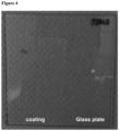
- Transparency evaluation When glass was used as a substrate, the degree to how well the background on the rear face is visible was rated as high, medium, or low. In particular, images obtained while evaluating the transparency for Examples, 1, 3, and 5, and Comparative Example 1 are shown in FIGS. 1 , 2 , 3 , and 4 , respectively.
- Light transmittance (%) evaluation When a PET film was used as a substrate, light transmittance was measured by using a color-difference meter.
- Moisture permeability evaluation When a PET film was used as a substrate, moisture permeation was evaluated by ASTM F1249 standards and corresponding equipment.
Landscapes
- Chemical & Material Sciences (AREA)
- Organic Chemistry (AREA)
- Engineering & Computer Science (AREA)
- Chemical Kinetics & Catalysis (AREA)
- Medicinal Chemistry (AREA)
- Polymers & Plastics (AREA)
- Health & Medical Sciences (AREA)
- Materials Engineering (AREA)
- Manufacturing & Machinery (AREA)
- Life Sciences & Earth Sciences (AREA)
- Wood Science & Technology (AREA)
- Dispersion Chemistry (AREA)
- Composite Materials (AREA)
- General Chemical & Material Sciences (AREA)
- Geochemistry & Mineralogy (AREA)
- Inorganic Chemistry (AREA)
- Microelectronics & Electronic Packaging (AREA)
- Compositions Of Macromolecular Compounds (AREA)
- Electroluminescent Light Sources (AREA)
- Paints Or Removers (AREA)
Description
- The present invention relates to a composition for a moisture permeation preventing film for an electronic device, a method for forming a moisture permeation preventing film for an electronic device using the same, and an electronic device.
- In general, glass materials are mainly used as the material for a moisture permeation preventing film for an electronic device when flexibility is not required, and when flexibility is required, film or ink materials are used.
- Meanwhile, regardless of the material, moisture permeation preventing films are generally formed in a multilayer structure in order to secure low moisture permeability which is the unique function of a moisture permeation preventing film for an electronic device.
WO2005/047746 describes a curable coating composition for forming a thermal insulating layer.JP2000043179 KR101288736 - However, in the case of moisture permeation preventing films manufactured by using glass materials or moisture permeation preventing films formed in a multilayer structure, flexibility is insufficiently low, the manufacturing process thereof is complex, and, as a result, problems of low productivity and price competitiveness happen due to increased manufacturing costs.
- The present inventors attempt to solve the problems described above by disclosing a composition for a moisture permeation preventing film for an electronic device including an aerogel.
- Moreover, a method for forming a moisture permeation preventing film for an electronic device in a simple process using the composition is disclosed, and in addition, an electronic device including the moisture permeation preventing film is disclosed.
- In one embodiment of the present invention, provided is a composition for a moisture permeation preventing film for an electronic device, comprising:
- 1 to 10 wt% of an aerogel that comprises silica;
- 10 to 50 wt% of a solvent;
- 0.1 to 5 wt% of an additive that is a surfactant, an antifoaming agent, or a mixture thereof;
- The solvent may be at least one selected from the group consisting of toluene, ethyl alcohol, methyl ethyl ketone (MEK), n-heptane, and isopropyl alcohol (IPA).
- The additive may be a surfactant, an antifoaming agent, or a mixture thereof.
- In the above description, the surfactant may be at least one selected from the group consisting of sodium alkyl diphenyloxide disulfonate, polyoxyethylene tridecyl ether sulfate, polyalkyleneoxide silane, sodium alkyl diphenyloxide disulfonate, and a fluoric surfactant.
- In addition, the antifoaming agent may be at least one selected from the group consisting of silicone, polysiloxane, polymethylsiloxane, modified polysiloxane, and ether-modified polysiloxane.
- In another embodiment of the present invention, provided is a method for forming a moisture permeation preventing film for an electronic device, comprising a step of preparing a composition for a moisture permeation preventing film for an electronic device, comprising 1 to 10 wt% of an aerogel that comprises silica, 10 to 50 wt% of a solvent, 0.1 to 5 wt% of an additive that is a surfactant, an antifoaming agent, or a mixture thereof, and a binder as the remainder, the binder comprising silicone oil or at least one selected from the group consisting of a silanol group, an alkoxysilyl group, and polydimethylsiloxane, in a molecule; a step of applying the composition for a moisture permeation preventing film for an electronic device on a substrate; and a step of drying the applied composition for a moisture permeation preventing film for an electronic device on the substrate.
- Hereinafter, each step of the method is described.
- In the step of applying the composition for a moisture permeation preventing film for an electronic device on a substrate, an application amount of the composition for a moisture permeation preventing film for an electronic device per area (m2) of each side of the substrate may be 135 to 1,227 g/m2.
- In still another embodiment of the present invention, provided is an electronic device including a substrate; and a moisture permeation preventing film for an electronic device, located on the substrate and including 1 to 10 wt% of an aerogel that comprises silica, 0.1 to 5 wt% of an additive that is a surfactant, an antifoaming agent, or a mixture thereof, and a binder as the remainder, the binder comprising silicone oil or at least one selected from the group consisting of a silanol group, an alkoxysilyl group, and polydimethylsiloxane, in a molecule.
- The moisture permeation preventing film for an electronic device is described as follows.
- The moisture permeation preventing film for an electronic device may have a thickness in a range of 100 to 900 µm.
- The moisture permeation preventing film for an electronic device may be formed as a single layer.
- The substrate is described as follows.
- The substrate may be a flexible board.
- The flexible board may consist of a material selected from the group consisting of polyethylene terephthalate (PET), polyacrylate (PA), polycarbonate (PC), polyethersulfone (PES), polyimide (PI), and a combination thereof.
- Independently, the substrate may be a rigid board.
- The rigid board may consist of a material selected from glass.
- Meanwhile, the electronic device may be a touch panel, a battery, or a display device.
- According to embodiments of the present invention, a composition for a moisture permeation preventing film for an electronic device which is capable of lowering moisture permeability by including an aerogel, thereby preventing deterioration of the function of the electronic device, and prolonging the lifespan thereof, a method for forming a moisture permeation preventing film using the same, and an electronic device can be provided.
- Furthermore, by securing excellent flexibility of the moisture permeation preventing film, applications for flexible, wearable, and display devices are possible, and the moisture permeation preventing film can be applied in various electronic devices such as touch panel sensors, batteries, and the like.
-
-
FIG. 1 is an image obtained while evaluating the transparency of a moisture permeation preventing film formed according to Example 1. -
FIG. 2 is an image obtained while evaluating the transparency of a moisture permeation preventing film formed according to Example 3. -
FIG. 3 is an image obtained while evaluating the transparency of a moisture permeation preventing film formed according to Example 5. -
FIG. 4 is an image obtained while evaluating the transparency of a moisture permeation preventing film formed according to Comparative Example 1. -
FIGS. 5 and6 are images obtained while evaluating the flexibility of a moisture permeation preventing film formed according to Example 5. - Hereinafter, embodiments of the present invention will be described in detail. However, as these embodiments are presented as examples, the present invention is not limited thereto, and the present invention is only defined by the scope of the claims to be described below.
- As specified in claim 1 the invention provides a composition for a moisture permeation preventing film for an electronic device.
- This corresponds to a composition for a moisture permeation preventing film for an electronic device, which, by including an aerogel (specifically, hydrophobic aerogel), is capable of lowering moisture permeability by including an aerogel, thereby preventing deterioration of the function of an electronic device and prolonging the lifespan thereof.
- Therefore, excellent flexibility of a moisture permeation preventing film can be secured, applications for flexible and/or wearable display devices are possible, and the moisture permeation preventing film can be advantageously applied in various electronic devices such as touch panel sensors, batteries, and the like.
- Hereinafter, the moisture permeation preventing film for an electronic device will be described in detail.
- As previously described, the composition for a moisture permeation preventing film for an electronic device includes 1 to 10 wt% of an aerogel; 10 to 50 wt% of a solvent; 0.1 to 5 wt% of an additive; and a binder as the remainder based on a total 100 wt% of the composition for a moisture permeation preventing film for an electronic device, and the reason for limiting the content of each material thereto is described as follows.
- When the content of an aerogel in the composition for a moisture permeation preventing film for an electronic device satisfies a range of 1 to 10 wt%, as previously described, there are cases in which moisture permeability of a moisture permeation preventing film can be lowered and flexibility is secured.
- However, at above 10 wt%, the viscosity of the composition becomes too high, and as a result, it is difficult to uniformly form a moisture permeation preventing film. Accordingly, a phenomenon in which the transparency and permeability of the formed moisture permeation preventing film are reduced may occur. On the contrary, at below 1 wt%, the content of the aerogel is too low to be expected to be effective.
- The content of the solvent in the composition for a moisture permeation preventing film for an electronic device satisfying a range of 10 to 50 wt% can result in the viscosity and density in which the binder, the aerogel, and the additive can be properly dispersed.
- However, at 50 wt% or above, due to the excessively high content of the solvent, the density of the composition decreases, which is a factor for increased moisture permeability of the moisture permeation preventing film thus formed. In contrast, in the case of below 10 wt%, the viscosity of the composition becomes too high, and as a result, it is difficult for each material to be uniformly dispersed, and the moisture permeation preventing film thus formed may contain bubbles which are difficult to be removed.
- Depending on the desired characteristics, the composition for a moisture permeation preventing film for an electronic device may include the additive at 0.1 wt% to 5 wt% therein.
- However, at above 5 wt%, the content of the aerogel relatively decreases, and as a result, the moisture permeability of the moisture permeation preventing film thus formed may decrease. In contrast, in the case of below 0.1 wt%, it is difficult for the moisture permeation preventing film to exhibit effectiveness due to the significantly low content thereof.
- Hereinafter, each component of the composition for a moisture permeation preventing film for an electronic device provided in one embodiment of the present invention is described in more detail.
- First, the aerogel is described as follows.
- A hydrophobic aerogel may contribute to significantly lowering the moisture permeability of a moisture permeation preventing film.
- More specifically, the aerogel includes silica, and in the examples described below, such silica aerogel is used.
- Although the particle diameter of the aerogel is not particularly limited, it is necessary for the diameter to be less than or equal to the thickness of the moisture permeation preventing film to be formed.
- The binder is described as follows.
- The binder may include silicone oil.
- Alternatively, the binder may include at least one selected from the group consisting of a silanol group, an alkoxysilyl group, and polydimethylsiloxane, in a molecule.
- The solvent, as previously described, is not particularly limited as long as the solvent is a material capable of dissolving and uniformly dispersing the aerogel, the binder, and the additive.
- For example, the solvent may be at least one selected from the group consisting of toluene, ethyl alcohol, methyl ethyl ketone (MEK), n-heptane, and isopropyl alcohol (IPA).
- In the cases of the examples described below, ethyl alcohol is used as the solvent.
- Meanwhile, the additive is described as follows.
- The additive is used to provide various functionalities to the composition for a moisture permeation preventing film for an electronic device or to improve the characteristics of the composition, and the additive may be a surfactant, an antifoaming agent, or a mixture thereof. That is, as the additive, the surfactant may be used alone, the antifoaming agent may be used alone, or a combination of the surfactant and the antifoaming agent may be used.
- In the above description, the surfactant may be at least one selected from the group consisting of sodium alkyl diphenyloxide disulfonate, polyoxyethylene tridecyl ether sulfate, polyalkyleneoxide silane, sodium alkyl diphenyloxide disulfonate, and a fluoric surfactant.
- That is, the surfactant may be selected as one substance among the listed substances or selected by combining two or more substances. In the examples described below, a fluoric surfactant is used as the surfactant.
- In addition, the antifoaming agent may include at least one selected from the group consisting of silicone, polysiloxane, polymethylsiloxane, modified polysiloxane, and ether-modified polysiloxane.
- That is, as the antifoaming agent, one substance among the listed substances may be selected or a combination of two or more substances among the listed substances may be selected. In the examples described below, a silicone antifoaming agent is used as the antifoaming agent.
- In another embodiment of the present invention, provided is a method for forming a moisture permeation preventing film for an electronic device, comprising a step of preparing a composition for a moisture permeation preventing film for an electronic device, comprising 1 to 10 wt% of an aerogel that comprises silica, 10 to 50 wt% of a solvent, 0.1 to 5 wt% of an additive that is a surfactant, an antifoaming agent, or a mixture thereof, and a binder as the remainder, the binder comprising silicone oil or at least one selected from the group consisting of a silanol group, an alkoxysilyl group, and polydimethylsiloxane, in a molecule; a step of applying the composition for a moisture permeation preventing film for an electronic device on a substrate; and a step of drying the applied composition for a moisture permeation preventing film for an electronic device on the substrate.
- Specifically, the moisture permeation preventing film for an electronic device may be identical to what was previously described. In this case, a method for forming a moisture permeation preventing film for an electronic device may be carried out as a simple process of preparing a composition by mixing the raw materials, applying the same on a substrate followed by drying, and the moisture permeation preventing film for an electronic device thus formed may have significant effects which are previously described.
- Hereinafter, repeated descriptions are omitted, and each step is described as follows.
- In the step of applying the composition for a moisture permeation preventing film for an electronic device on a substrate, an application amount of the composition for a moisture permeation preventing film for an electronic device per area (m2) of each side of the substrate may be in a range of 135 to 1,227 g/m2.
- When the application amount satisfies the above range, the thickness of the finally formed moisture permeation preventing film may be 100 to 900 µm, and this is the range of thickness which can secure flexibility as well as realize an excellent effect of preventing moisture permeation.
- On the other hand, when the application amount of the composition of a moisture permeation preventing film for an electronic device per area (m2) of each side of the substrate is less than 135 g/m2, the moisture permeation preventing film is formed with a small thickness of less than 100 µm, and as a result, the effectiveness of a moisture permeation preventing film may be insignificant. In addition, when the application amount of the composition of a moisture permeation preventing film for an electronic device per area of each side of the substrate is greater than 1,227 g/m2, the moisture permeation preventing film is formed with an excessively large thickness exceeding 900 µm, and as a result, flexibility and permeability of a moisture permeation preventing film cannot be secured.
- Meanwhile, the step of drying the applied composition for a moisture permeation preventing film for an electronic device on the substrate may be carried out at a temperature in a range of 80 to 140 °C for 1 to 3 hours, and in this process, the solvent in the composition of a moisture permeation preventing film for an electronic device applied on the substrate is removed, and a moisture permeation preventing film consisting of the remaining components can be formed.
- In still another embodiment of the present invention, provided is an electronic device including a substrate; and a moisture permeation preventing film for an electronic device, located on the substrate and comprising 1 to 10 wt% of an aerogel that comprises silica, 0.1 to 5 wt% of an additive that is a surfactant, an antifoaming agent, or a mixture thereof, and a binder as the remainder, the binder comprising silicone oil or at least one selected from the group consisting of a silanol group, an alkoxysilyl group, and polydimethylsiloxane, in a molecule.
- Specifically, the moisture permeation preventing film for an electronic device may be formed by using the previously described method for forming a moisture permeation preventing film for an electronic device and the previously described composition of a moisture permeation preventing film for an electronic device.
- Hereinafter, repeated descriptions are omitted, and each component of the electronic device is described as follows.
- The moisture permeation preventing film for an electronic device is described as follows.
- The thickness of the moisture permeation preventing film for an electronic device may be 100 to 900 µm, but is not particularly limited thereto. As previously described, at below 100 µm, the thickness thereof is too small, thereby it is difficult to expect an effect of preventing moisture permeation, and at above 900 µm, the thickness thereof is too large and may affect flexibility.
- The moisture permeation preventing film for an electronic device may be formed as a single layer. Specifically, although formed as a single layer instead of a multilayer structure, the moisture permeation preventing film for an electronic device which satisfies the composition as defined above may manifest an excellent function of preventing moisture permeation. Furthermore, as previously described, a moisture permeation preventing film formed as a multilayer structure has insufficient flexibility, but the moisture permeation preventing film formed as a single layer may have excellent flexibility.
- The substrate is described as follows.
- The substrate may be a flexible board. In this case, applications for flexible and/or wearable and display devices are possible.
- The flexible board, which is not particularly limited as long as it is a material with flexibility, may consist of a material selected from the group consisting of polyethylene terephthalate (PET), polyacrylate (PA), polycarbonate (PC), polyethersulfone (PES), polyimide (PI), and a combination thereof.
- Independently, the substrate may be a rigid board. This refers to a board which is commonly used today.
- The rigid board, which is not particularly limited as long as it consists of a material without flexibility, may consist of a material selected from glass.
- Meanwhile, the electronic device may be a touch panel, a battery or a display device, and examples of the display device include a liquid crystal display (LCD), a light emitting diode (LED), an organic light-emitting diode (OLED), and the like. As such, application to various electronic devices is possible.
- Hereinafter, the examples of the present invention and the experimental examples therefor are described below. However, the following examples are merely preferred examples of the present invention, and the present invention is not limited to the following examples.
- First, compositions of a moisture permeation preventing film for an electronic device were prepared by mixing raw materials according to compositions as shown in Table 1 below.
- Specifically, for the raw materials, silicone oil (Manufacturer: Shinetsu) was used as a binder, a silica aerogel (Manufacturer: JIOS AEROGEL) was used as an aerogel, ethyl alcohol (Manufacturer: Daejung Chemicals & Metals) was used as a solvent, a silicone antifoaming agent (Manufacturer: AIR PRODUCTS) was used as an antifoaming agent, and a fluoric surfactant (Manufacturer: Momentive) was used as a surfactant.
- Afterwards, the prepared composition of a moisture permeation preventing film for an electronic device was applied on a substrate and dried for 2 hours in a dry oven in which the temperature was adjusted to be at 110 °C, in order to form each moisture permeation preventing film having a thickness of 500 µm.
- At this time, depending on evaluation type, for the substrate, a commercially available PET film, which is a type of flexible board, having a width of 5 cm, a length of 5 cm, and a thickness of 100 µm was used, or commercially available glass, which is a type of rigid board, was used by cutting the same to a width of 10 cm, a length of 10 cm, and a thickness of 3 mm.
- In addition, the application amount per area of each side of the substrate was 520 g/m2, and the thickness of the moisture permeation preventing film thus formed was 500 µm. However, in the case of the evaluation of transparency as described below, a moisture permeation preventing film was formed only on a half of a face of the substrate to compare a part on which a moisture permeation preventing film was formed and a part on which a moisture permeation preventing film was not formed for evaluation.
- As shown in Table 1 below, a moisture permeation preventing film was formed on a substrate in the same manner as in Examples 1 to 5, except that only a binder was used.
Table 1 Classification Binder Solvent Aerogel Surfactant Antifoaming agent Comparative Example 1 100 - - - Example 1 87.5 10 1 1 0.5 Example 2 85.5 3 1 0.5 Example 3 83.5 5 1 0.5 Example 4 81.5 7 1 0.5 Example 5 78.5 10 1 0.5 Note: In the above table, the content of each material was indicated as wt% based on a total 100 wt% of the composition. - Each moisture permeation preventing film formed in Examples 1 to 5 and Comparative Example 1 was evaluated for transparency, flexibility, light transmittance (%), and moisture permeability (g/m2·day), and the result is shown in Table 2 below.
Table 2 Classification Transparency Flexibility Light transmittance (%) Moisture permeability (g/m2·day) Comparative Example 1 High High 95.8 14.4 Example 1 High High 91.3 14.08 Example 2 High High 90.4 12.95 Example 3 High High 90.9 11.22 Example 4 Medium High 88.4 11.09 Example 5 Medium High 84.5 9.75 - Specifically, the conditions for each evaluation are as follows.
- Transparency evaluation: When glass was used as a substrate, the degree to how well the background on the rear face is visible was rated as high, medium, or low. In particular, images obtained while evaluating the transparency for Examples, 1, 3, and 5, and Comparative Example 1 are shown in
FIGS. 1 ,2 ,3 , and4 , respectively. - Flexibility evaluation: When a PET film was used as a substrate, the degree to which damage occurred on surface or whether the moisture permeation film was separated, when bending at 90° or more was rated as high, medium, or low. In particular, images obtained when evaluating the flexibility according to Example 5 are shown in
FIGS. 5 and6 . - Light transmittance (%) evaluation: When a PET film was used as a substrate, light transmittance was measured by using a color-difference meter.
- Moisture permeability evaluation: When a PET film was used as a substrate, moisture permeation was evaluated by ASTM F1249 standards and corresponding equipment.
- Through such evaluation results, in Examples 1 to 5 where the composition including a silica aerogel and additives as well as a binder was applied as a moisture permeation preventing film, similar flexibility compared to Comparative Example 1, where only a binder was applied as a moisture permeation preventing film, was secured, and also transparency and light transmittance were reduced. In particular, it was found that moisture permeability which is a characteristic essentially required to be low in moisture permeation preventing films was significantly reduced.
Claims (12)
- A composition for a moisture permeation preventing film for an electronic device, comprising:1 to 10 wt% of an aerogel that comprises silica;10 to 50 wt% of a solvent;0.1 to 5 wt% of an additive that is a surfactant, an antifoaming agent, or a mixture thereof; anda binder as the remainder, the binder comprising silicone oil or at least one selected from the group consisting of a silanol group, an alkoxysilyl group, and polydimethylsiloxane, in a molecule.
- The composition of claim 1, wherein the solvent is at least one selected from the group consisting of toluene, ethyl alcohol, methyl ethyl ketone (MEK), n-heptane, and isopropyl alcohol (IPA).
- The composition of claim 1, wherein the surfactant is at least one selected from the group consisting of sodium alkyl diphenyloxide disulfonate, polyoxyethylene tridecyl ether sulfate, polyalkyleneoxide silane, sodium alkyl diphenyloxide disulfonate, and a fluoric surfactant or the antifoaming agent is at least one selected from the group consisting of silicone, polysiloxane, polymethylsiloxane, modified polysiloxane, and ether-modified polysiloxane.
- A method for forming a moisture permeation preventing film for an electronic device, comprising:a step of preparing a composition for a moisture permeation preventing film for an electronic device, comprising 1 to 10 wt% of an aerogel that comprises silica, 10 to 50 wt% of a solvent, 0.1 to 5 wt% of an additive that is a surfactant, an antifoaming agent, or a mixture thereof, and a binder as the remainder, the binder comprising silicone oil or at least one selected from the group consisting of a silanol group, an alkoxysilyl group, and polydimethylsiloxane, in a molecule;a step of applying the composition for a moisture permeation preventing film for an electronic device on a substrate; anda step of drying the composition for a moisture permeation preventing film for an electronic device that has been applied on the substrate.
- The method of claim 4, wherein, in the step of applying the composition for a moisture permeation preventing film for an electronic device on a substrate, an application amount of the composition for a moisture permeation preventing film for an electronic device per area (m2) of each side of the substrate is 135 to 1,227 g/m2.
- An electronic device comprising:a substrate; anda moisture permeation preventing film for an electronic device located on the substrate and, comprising 1 to 10 wt% of an aerogel that comprises silica, 0.1 to 5 wt% of an additive that is a surfactant, an antifoaming agent, or a mixture thereof, and a binder as the remainder, the binder comprising silicone oil or at least one selected from the group consisting of a silanol group, an alkoxysilyl group, and polydimethylsiloxane, in a molecule.
- The electronic device of claim 6, wherein the moisture permeation preventing film for an electronic device has a thickness in a range of 100 to 900 µm.
- The electronic device of claim 6, wherein the moisture permeation preventing film for an electronic device is formed as a single layer.
- The electronic device of claim 6, wherein the substrate is a flexible board.
- The electronic device of claim 9, wherein the flexible board consists of a material selected from the group consisting of polyethylene terephthalate (PET), polyacrylate (PA), polycarbonate (PC), polyethersulfone (PES), polyimide (PI), and a combination thereof.
- The electronic device of claim 6, wherein the substrate is a rigid board including glass.
- The electronic device of claim 6, wherein the electronic device is a touch panel, a battery, or a display device.
Applications Claiming Priority (1)
| Application Number | Priority Date | Filing Date | Title |
|---|---|---|---|
| PCT/KR2015/005885 WO2016199957A1 (en) | 2015-06-11 | 2015-06-11 | Composition for moisture permeation preventing film for electronic device, method for forming moisture permeation preventing film for electronic device using same, and electronic device |
Publications (3)
| Publication Number | Publication Date |
|---|---|
| EP3310136A1 EP3310136A1 (en) | 2018-04-18 |
| EP3310136A4 EP3310136A4 (en) | 2018-12-12 |
| EP3310136B1 true EP3310136B1 (en) | 2023-04-26 |
Family
ID=57503657
Family Applications (1)
| Application Number | Title | Priority Date | Filing Date |
|---|---|---|---|
| EP15895025.3A Active EP3310136B1 (en) | 2015-06-11 | 2015-06-11 | Composition for moisture permeation preventing film for electronic device, method for forming moisture permeation preventing film for electronic device using same, and electronic device |
Country Status (3)
| Country | Link |
|---|---|
| US (2) | US20180100051A1 (en) |
| EP (1) | EP3310136B1 (en) |
| WO (1) | WO2016199957A1 (en) |
Families Citing this family (1)
| Publication number | Priority date | Publication date | Assignee | Title |
|---|---|---|---|---|
| CN119569476A (en) | 2023-09-07 | 2025-03-07 | 欧文斯科宁知识产权资产有限公司 | Aerogel composite and method for manufacturing aerogel composite |
Family Cites Families (11)
| Publication number | Priority date | Publication date | Assignee | Title |
|---|---|---|---|---|
| JP2000043179A (en) * | 1998-07-28 | 2000-02-15 | Asahi Chem Ind Co Ltd | Humidity-controllable sheet |
| US6806299B2 (en) * | 2001-05-18 | 2004-10-19 | The Regents Of The University Of California | Preparation of hydrophobic organic aeorgels |
| RU2006120287A (en) * | 2003-11-12 | 2008-01-10 | Дж Стюарт Мл. БЕРЧИЛЛ (US) | COMPOSITION FOR A THERMAL INSULATING LAYER |
| WO2007086819A2 (en) * | 2004-11-24 | 2007-08-02 | Aspen Aerogels, Inc. | High strength aerogel panels |
| US20070027232A1 (en) * | 2005-07-27 | 2007-02-01 | Chemcoat, Inc. | Coating compositions incorporating nanotechnology and methods for making same |
| KR20090010907U (en) * | 2008-04-22 | 2009-10-27 | 김기철 | Self-adhesive insulation sheet and waterproof method using the same |
| FR2968937B1 (en) * | 2010-12-21 | 2012-12-14 | Oreal | COSMETIC COMPOSITION COMPRISING SILICA AEROGEL PARTICLES |
| FR2981566B1 (en) * | 2011-10-21 | 2013-11-08 | Oreal | COSMETIC COMPOSITION COMPRISING SILICA AEROGEL PARTICLES, A GEMINE SURFACTANT AND A SOLID FATTY BODY |
| KR101288736B1 (en) * | 2012-08-16 | 2013-07-29 | 주식회사 엠쓰리텍 | Aerogel paste and method to manufacture thereof |
| KR20140135394A (en) * | 2013-05-16 | 2014-11-26 | 주식회사 빅스 | Method of manufacturing polyurethane resin comprising airogel used in moisture permeable-waterproof fabric |
| KR101460242B1 (en) * | 2013-09-10 | 2014-11-10 | 주식회사 에스바텍 | The adhesive film for fixing the module of mobile device, which has impact resistance and water resistance |
-
2015
- 2015-06-11 WO PCT/KR2015/005885 patent/WO2016199957A1/en not_active Ceased
- 2015-06-11 EP EP15895025.3A patent/EP3310136B1/en active Active
-
2017
- 2017-12-11 US US15/837,913 patent/US20180100051A1/en not_active Abandoned
-
2022
- 2022-01-07 US US17/571,386 patent/US20220306833A1/en active Pending
Also Published As
| Publication number | Publication date |
|---|---|
| EP3310136A4 (en) | 2018-12-12 |
| US20220306833A1 (en) | 2022-09-29 |
| EP3310136A1 (en) | 2018-04-18 |
| US20180100051A1 (en) | 2018-04-12 |
| WO2016199957A1 (en) | 2016-12-15 |
Similar Documents
| Publication | Publication Date | Title |
|---|---|---|
| TWI567157B (en) | Antistatic surface protection film manufacturing method and antistatic surface protection film | |
| KR20140110325A (en) | Scattering protecting film with excellent optical properties and scratch resistance and method of manufacturing the same | |
| US20190064397A1 (en) | Refractive-index-matching thin film | |
| TW201435925A (en) | Stabilization agents for silver nanowire based transparent conductive films | |
| KR20150065597A (en) | Transparent conductor, method for preparing the same, and optical display including the same | |
| KR20160078137A (en) | Transparent electrodes and electronic decives including the same | |
| CN103886934A (en) | Transparent conducting film | |
| KR101888223B1 (en) | Scattering protecting film and method for preparing the same | |
| TW201429713A (en) | Stabilization agents for transparent conductive films | |
| US20220306833A1 (en) | Composition for moisture permeation preventing film for electronic device, method for forming moisture permeation preventing film for electronic device using same, and electronic device | |
| CN110114421B (en) | Water-repellent coating composition and water-repellent coated substrate coated with the same | |
| JP2017522581A (en) | Low refractive composition, method for producing the same, and transparent conductive film | |
| KR102151435B1 (en) | Heat-curing composition having a flame retardant property and an antistatic property, method of coating using the same, and coating substrate comprising the same | |
| KR102268490B1 (en) | Thermosetting resin composition, cured product thereof and display member using the same | |
| KR101780727B1 (en) | Moisture-proof film composition for electronic equipment, method for manufacturing moisture-proof film using the same composition, and electronic equipment | |
| KR101567223B1 (en) | Polyester film for optical use | |
| TW201545878A (en) | Polyester film and transparent electrode film using thereof | |
| KR102392098B1 (en) | Release film and manufacturing method thereof | |
| KR20160034577A (en) | Manufacturing method of energy saving transparent paint | |
| CN106010325B (en) | Surface protection film and optical component attached with the surface protection film | |
| KR102367063B1 (en) | Hard Coating Composition and Hard Coating Film Using the Same | |
| KR102064997B1 (en) | Protective film compound manufacturing method and transparent electrode manufacturing method | |
| KR20230097680A (en) | Anti-static silicone release film with good anti-blocking characteristics | |
| KR101965896B1 (en) | Hard coating composition and scattering protecting film using the same | |
| KR101705642B1 (en) | Transparant conductive film |
Legal Events
| Date | Code | Title | Description |
|---|---|---|---|
| STAA | Information on the status of an ep patent application or granted ep patent |
Free format text: STATUS: THE INTERNATIONAL PUBLICATION HAS BEEN MADE |
|
| PUAI | Public reference made under article 153(3) epc to a published international application that has entered the european phase |
Free format text: ORIGINAL CODE: 0009012 |
|
| STAA | Information on the status of an ep patent application or granted ep patent |
Free format text: STATUS: REQUEST FOR EXAMINATION WAS MADE |
|
| 17P | Request for examination filed |
Effective date: 20180108 |
|
| AK | Designated contracting states |
Kind code of ref document: A1 Designated state(s): AL AT BE BG CH CY CZ DE DK EE ES FI FR GB GR HR HU IE IS IT LI LT LU LV MC MK MT NL NO PL PT RO RS SE SI SK SM TR |
|
| AX | Request for extension of the european patent |
Extension state: BA ME |
|
| DAV | Request for validation of the european patent (deleted) | ||
| DAX | Request for extension of the european patent (deleted) | ||
| RIC1 | Information provided on ipc code assigned before grant |
Ipc: C09D 7/61 20180101ALI20181031BHEP Ipc: H05K 3/28 20060101AFI20181031BHEP Ipc: H01L 51/52 20060101ALI20181031BHEP Ipc: C09D 5/00 20060101ALI20181031BHEP Ipc: C08J 9/00 20060101ALI20181031BHEP Ipc: C08J 5/18 20060101ALI20181031BHEP Ipc: B32B 27/06 20060101ALI20181031BHEP |
|
| A4 | Supplementary search report drawn up and despatched |
Effective date: 20181109 |
|
| STAA | Information on the status of an ep patent application or granted ep patent |
Free format text: STATUS: EXAMINATION IS IN PROGRESS |
|
| 17Q | First examination report despatched |
Effective date: 20220131 |
|
| INTG | Intention to grant announced |
Effective date: 20221117 |
|
| RIN1 | Information on inventor provided before grant (corrected) |
Inventor name: PARK, DO YOUNG Inventor name: JUNG, DONG HO Inventor name: LEE, MUN HYEONG Inventor name: HAHN, CHOON SOO Inventor name: KIM, MIN WOO Inventor name: PARK, JONG CHUL Inventor name: JOUNG, YOUNG CHUL Inventor name: ROH, MYUNG JE |
|
| GRAS | Grant fee paid |
Free format text: ORIGINAL CODE: EPIDOSNIGR3 |
|
| STAA | Information on the status of an ep patent application or granted ep patent |
Free format text: STATUS: GRANT OF PATENT IS INTENDED |
|
| GRAA | (expected) grant |
Free format text: ORIGINAL CODE: 0009210 |
|
| STAA | Information on the status of an ep patent application or granted ep patent |
Free format text: STATUS: THE PATENT HAS BEEN GRANTED |
|
| AK | Designated contracting states |
Kind code of ref document: B1 Designated state(s): AL AT BE BG CH CY CZ DE DK EE ES FI FR GB GR HR HU IE IS IT LI LT LU LV MC MK MT NL NO PL PT RO RS SE SI SK SM TR |
|
| RAP1 | Party data changed (applicant data changed or rights of an application transferred) |
Owner name: AEROGEL R&D PTE. LTD. |
|
| REG | Reference to a national code |
Ref country code: GB Ref legal event code: FG4D |
|
| REG | Reference to a national code |
Ref country code: CH Ref legal event code: EP |
|
| REG | Reference to a national code |
Ref country code: DE Ref legal event code: R096 Ref document number: 602015083355 Country of ref document: DE |
|
| REG | Reference to a national code |
Ref country code: AT Ref legal event code: REF Ref document number: 1563790 Country of ref document: AT Kind code of ref document: T Effective date: 20230515 |
|
| REG | Reference to a national code |
Ref country code: IE Ref legal event code: FG4D |
|
| REG | Reference to a national code |
Ref country code: LT Ref legal event code: MG9D |
|
| REG | Reference to a national code |
Ref country code: NL Ref legal event code: MP Effective date: 20230426 |
|
| P01 | Opt-out of the competence of the unified patent court (upc) registered |
Effective date: 20230728 |
|
| REG | Reference to a national code |
Ref country code: AT Ref legal event code: MK05 Ref document number: 1563790 Country of ref document: AT Kind code of ref document: T Effective date: 20230426 |
|
| P02 | Opt-out of the competence of the unified patent court (upc) changed |
Effective date: 20230811 |
|
| PG25 | Lapsed in a contracting state [announced via postgrant information from national office to epo] |
Ref country code: NL Free format text: LAPSE BECAUSE OF FAILURE TO SUBMIT A TRANSLATION OF THE DESCRIPTION OR TO PAY THE FEE WITHIN THE PRESCRIBED TIME-LIMIT Effective date: 20230426 |
|
| PG25 | Lapsed in a contracting state [announced via postgrant information from national office to epo] |
Ref country code: SE Free format text: LAPSE BECAUSE OF FAILURE TO SUBMIT A TRANSLATION OF THE DESCRIPTION OR TO PAY THE FEE WITHIN THE PRESCRIBED TIME-LIMIT Effective date: 20230426 Ref country code: PT Free format text: LAPSE BECAUSE OF FAILURE TO SUBMIT A TRANSLATION OF THE DESCRIPTION OR TO PAY THE FEE WITHIN THE PRESCRIBED TIME-LIMIT Effective date: 20230828 Ref country code: NO Free format text: LAPSE BECAUSE OF FAILURE TO SUBMIT A TRANSLATION OF THE DESCRIPTION OR TO PAY THE FEE WITHIN THE PRESCRIBED TIME-LIMIT Effective date: 20230726 Ref country code: ES Free format text: LAPSE BECAUSE OF FAILURE TO SUBMIT A TRANSLATION OF THE DESCRIPTION OR TO PAY THE FEE WITHIN THE PRESCRIBED TIME-LIMIT Effective date: 20230426 Ref country code: AT Free format text: LAPSE BECAUSE OF FAILURE TO SUBMIT A TRANSLATION OF THE DESCRIPTION OR TO PAY THE FEE WITHIN THE PRESCRIBED TIME-LIMIT Effective date: 20230426 |
|
| PG25 | Lapsed in a contracting state [announced via postgrant information from national office to epo] |
Ref country code: RS Free format text: LAPSE BECAUSE OF FAILURE TO SUBMIT A TRANSLATION OF THE DESCRIPTION OR TO PAY THE FEE WITHIN THE PRESCRIBED TIME-LIMIT Effective date: 20230426 Ref country code: PL Free format text: LAPSE BECAUSE OF FAILURE TO SUBMIT A TRANSLATION OF THE DESCRIPTION OR TO PAY THE FEE WITHIN THE PRESCRIBED TIME-LIMIT Effective date: 20230426 Ref country code: LV Free format text: LAPSE BECAUSE OF FAILURE TO SUBMIT A TRANSLATION OF THE DESCRIPTION OR TO PAY THE FEE WITHIN THE PRESCRIBED TIME-LIMIT Effective date: 20230426 Ref country code: LT Free format text: LAPSE BECAUSE OF FAILURE TO SUBMIT A TRANSLATION OF THE DESCRIPTION OR TO PAY THE FEE WITHIN THE PRESCRIBED TIME-LIMIT Effective date: 20230426 Ref country code: IS Free format text: LAPSE BECAUSE OF FAILURE TO SUBMIT A TRANSLATION OF THE DESCRIPTION OR TO PAY THE FEE WITHIN THE PRESCRIBED TIME-LIMIT Effective date: 20230826 Ref country code: HR Free format text: LAPSE BECAUSE OF FAILURE TO SUBMIT A TRANSLATION OF THE DESCRIPTION OR TO PAY THE FEE WITHIN THE PRESCRIBED TIME-LIMIT Effective date: 20230426 Ref country code: GR Free format text: LAPSE BECAUSE OF FAILURE TO SUBMIT A TRANSLATION OF THE DESCRIPTION OR TO PAY THE FEE WITHIN THE PRESCRIBED TIME-LIMIT Effective date: 20230727 |
|
| PG25 | Lapsed in a contracting state [announced via postgrant information from national office to epo] |
Ref country code: FI Free format text: LAPSE BECAUSE OF FAILURE TO SUBMIT A TRANSLATION OF THE DESCRIPTION OR TO PAY THE FEE WITHIN THE PRESCRIBED TIME-LIMIT Effective date: 20230426 |
|
| PG25 | Lapsed in a contracting state [announced via postgrant information from national office to epo] |
Ref country code: SK Free format text: LAPSE BECAUSE OF FAILURE TO SUBMIT A TRANSLATION OF THE DESCRIPTION OR TO PAY THE FEE WITHIN THE PRESCRIBED TIME-LIMIT Effective date: 20230426 |
|
| PG25 | Lapsed in a contracting state [announced via postgrant information from national office to epo] |
Ref country code: MC Free format text: LAPSE BECAUSE OF FAILURE TO SUBMIT A TRANSLATION OF THE DESCRIPTION OR TO PAY THE FEE WITHIN THE PRESCRIBED TIME-LIMIT Effective date: 20230426 |
|
| REG | Reference to a national code |
Ref country code: DE Ref legal event code: R097 Ref document number: 602015083355 Country of ref document: DE |
|
| PG25 | Lapsed in a contracting state [announced via postgrant information from national office to epo] |
Ref country code: SM Free format text: LAPSE BECAUSE OF FAILURE TO SUBMIT A TRANSLATION OF THE DESCRIPTION OR TO PAY THE FEE WITHIN THE PRESCRIBED TIME-LIMIT Effective date: 20230426 Ref country code: SK Free format text: LAPSE BECAUSE OF FAILURE TO SUBMIT A TRANSLATION OF THE DESCRIPTION OR TO PAY THE FEE WITHIN THE PRESCRIBED TIME-LIMIT Effective date: 20230426 Ref country code: RO Free format text: LAPSE BECAUSE OF FAILURE TO SUBMIT A TRANSLATION OF THE DESCRIPTION OR TO PAY THE FEE WITHIN THE PRESCRIBED TIME-LIMIT Effective date: 20230426 Ref country code: MC Free format text: LAPSE BECAUSE OF FAILURE TO SUBMIT A TRANSLATION OF THE DESCRIPTION OR TO PAY THE FEE WITHIN THE PRESCRIBED TIME-LIMIT Effective date: 20230426 Ref country code: EE Free format text: LAPSE BECAUSE OF FAILURE TO SUBMIT A TRANSLATION OF THE DESCRIPTION OR TO PAY THE FEE WITHIN THE PRESCRIBED TIME-LIMIT Effective date: 20230426 Ref country code: DK Free format text: LAPSE BECAUSE OF FAILURE TO SUBMIT A TRANSLATION OF THE DESCRIPTION OR TO PAY THE FEE WITHIN THE PRESCRIBED TIME-LIMIT Effective date: 20230426 Ref country code: CZ Free format text: LAPSE BECAUSE OF FAILURE TO SUBMIT A TRANSLATION OF THE DESCRIPTION OR TO PAY THE FEE WITHIN THE PRESCRIBED TIME-LIMIT Effective date: 20230426 |
|
| REG | Reference to a national code |
Ref country code: CH Ref legal event code: PL |
|
| REG | Reference to a national code |
Ref country code: BE Ref legal event code: MM Effective date: 20230630 |
|
| PG25 | Lapsed in a contracting state [announced via postgrant information from national office to epo] |
Ref country code: LU Free format text: LAPSE BECAUSE OF NON-PAYMENT OF DUE FEES Effective date: 20230611 |
|
| PLBE | No opposition filed within time limit |
Free format text: ORIGINAL CODE: 0009261 |
|
| STAA | Information on the status of an ep patent application or granted ep patent |
Free format text: STATUS: NO OPPOSITION FILED WITHIN TIME LIMIT |
|
| REG | Reference to a national code |
Ref country code: IE Ref legal event code: MM4A |
|
| PG25 | Lapsed in a contracting state [announced via postgrant information from national office to epo] |
Ref country code: LU Free format text: LAPSE BECAUSE OF NON-PAYMENT OF DUE FEES Effective date: 20230611 |
|
| 26N | No opposition filed |
Effective date: 20240129 |
|
| PG25 | Lapsed in a contracting state [announced via postgrant information from national office to epo] |
Ref country code: IE Free format text: LAPSE BECAUSE OF NON-PAYMENT OF DUE FEES Effective date: 20230611 |
|
| PG25 | Lapsed in a contracting state [announced via postgrant information from national office to epo] |
Ref country code: IE Free format text: LAPSE BECAUSE OF NON-PAYMENT OF DUE FEES Effective date: 20230611 Ref country code: CH Free format text: LAPSE BECAUSE OF NON-PAYMENT OF DUE FEES Effective date: 20230630 |
|
| PG25 | Lapsed in a contracting state [announced via postgrant information from national office to epo] |
Ref country code: SI Free format text: LAPSE BECAUSE OF FAILURE TO SUBMIT A TRANSLATION OF THE DESCRIPTION OR TO PAY THE FEE WITHIN THE PRESCRIBED TIME-LIMIT Effective date: 20230426 |
|
| PG25 | Lapsed in a contracting state [announced via postgrant information from national office to epo] |
Ref country code: SI Free format text: LAPSE BECAUSE OF FAILURE TO SUBMIT A TRANSLATION OF THE DESCRIPTION OR TO PAY THE FEE WITHIN THE PRESCRIBED TIME-LIMIT Effective date: 20230426 Ref country code: IT Free format text: LAPSE BECAUSE OF FAILURE TO SUBMIT A TRANSLATION OF THE DESCRIPTION OR TO PAY THE FEE WITHIN THE PRESCRIBED TIME-LIMIT Effective date: 20230426 Ref country code: BE Free format text: LAPSE BECAUSE OF NON-PAYMENT OF DUE FEES Effective date: 20230630 |
|
| PG25 | Lapsed in a contracting state [announced via postgrant information from national office to epo] |
Ref country code: BG Free format text: LAPSE BECAUSE OF FAILURE TO SUBMIT A TRANSLATION OF THE DESCRIPTION OR TO PAY THE FEE WITHIN THE PRESCRIBED TIME-LIMIT Effective date: 20230426 |
|
| PG25 | Lapsed in a contracting state [announced via postgrant information from national office to epo] |
Ref country code: BG Free format text: LAPSE BECAUSE OF FAILURE TO SUBMIT A TRANSLATION OF THE DESCRIPTION OR TO PAY THE FEE WITHIN THE PRESCRIBED TIME-LIMIT Effective date: 20230426 |
|
| PGFP | Annual fee paid to national office [announced via postgrant information from national office to epo] |
Ref country code: DE Payment date: 20250512 Year of fee payment: 11 |
|
| PGFP | Annual fee paid to national office [announced via postgrant information from national office to epo] |
Ref country code: GB Payment date: 20250513 Year of fee payment: 11 |
|
| PGFP | Annual fee paid to national office [announced via postgrant information from national office to epo] |
Ref country code: FR Payment date: 20250509 Year of fee payment: 11 |
|
| PG25 | Lapsed in a contracting state [announced via postgrant information from national office to epo] |
Ref country code: CY Free format text: LAPSE BECAUSE OF FAILURE TO SUBMIT A TRANSLATION OF THE DESCRIPTION OR TO PAY THE FEE WITHIN THE PRESCRIBED TIME-LIMIT; INVALID AB INITIO Effective date: 20150611 |
|
| PG25 | Lapsed in a contracting state [announced via postgrant information from national office to epo] |
Ref country code: HU Free format text: LAPSE BECAUSE OF FAILURE TO SUBMIT A TRANSLATION OF THE DESCRIPTION OR TO PAY THE FEE WITHIN THE PRESCRIBED TIME-LIMIT; INVALID AB INITIO Effective date: 20150611 |
|
| PG25 | Lapsed in a contracting state [announced via postgrant information from national office to epo] |
Ref country code: TR Free format text: LAPSE BECAUSE OF FAILURE TO SUBMIT A TRANSLATION OF THE DESCRIPTION OR TO PAY THE FEE WITHIN THE PRESCRIBED TIME-LIMIT Effective date: 20230426 |