EP3309896A1 - Ball-grid-array radio-frequency integrated-circuit printed-circuit-board assembly for automated vehicles - Google Patents
Ball-grid-array radio-frequency integrated-circuit printed-circuit-board assembly for automated vehicles Download PDFInfo
- Publication number
- EP3309896A1 EP3309896A1 EP17194590.0A EP17194590A EP3309896A1 EP 3309896 A1 EP3309896 A1 EP 3309896A1 EP 17194590 A EP17194590 A EP 17194590A EP 3309896 A1 EP3309896 A1 EP 3309896A1
- Authority
- EP
- European Patent Office
- Prior art keywords
- signal
- metal layer
- substrate
- slot
- solder
- Prior art date
- Legal status (The legal status is an assumption and is not a legal conclusion. Google has not performed a legal analysis and makes no representation as to the accuracy of the status listed.)
- Granted
Links
Images

Classifications
-
- H—ELECTRICITY
- H10—SEMICONDUCTOR DEVICES; ELECTRIC SOLID-STATE DEVICES NOT OTHERWISE PROVIDED FOR
- H10W—GENERIC PACKAGES, INTERCONNECTIONS, CONNECTORS OR OTHER CONSTRUCTIONAL DETAILS OF DEVICES COVERED BY CLASS H10
- H10W90/00—Package configurations
- H10W90/701—Package configurations characterised by the relative positions of pads or connectors relative to package parts
-
- H—ELECTRICITY
- H01—ELECTRIC ELEMENTS
- H01P—WAVEGUIDES; RESONATORS, LINES, OR OTHER DEVICES OF THE WAVEGUIDE TYPE
- H01P5/00—Coupling devices of the waveguide type
- H01P5/08—Coupling devices of the waveguide type for linking dissimilar lines or devices
-
- H—ELECTRICITY
- H01—ELECTRIC ELEMENTS
- H01P—WAVEGUIDES; RESONATORS, LINES, OR OTHER DEVICES OF THE WAVEGUIDE TYPE
- H01P3/00—Waveguides; Transmission lines of the waveguide type
- H01P3/10—Wire waveguides, i.e. with a single solid longitudinal conductor
-
- H—ELECTRICITY
- H01—ELECTRIC ELEMENTS
- H01P—WAVEGUIDES; RESONATORS, LINES, OR OTHER DEVICES OF THE WAVEGUIDE TYPE
- H01P3/00—Waveguides; Transmission lines of the waveguide type
- H01P3/12—Hollow waveguides
- H01P3/121—Hollow waveguides integrated in a substrate
-
- H—ELECTRICITY
- H01—ELECTRIC ELEMENTS
- H01P—WAVEGUIDES; RESONATORS, LINES, OR OTHER DEVICES OF THE WAVEGUIDE TYPE
- H01P5/00—Coupling devices of the waveguide type
- H01P5/08—Coupling devices of the waveguide type for linking dissimilar lines or devices
- H01P5/10—Coupling devices of the waveguide type for linking dissimilar lines or devices for coupling balanced lines or devices with unbalanced lines or devices
- H01P5/107—Hollow-waveguide/strip-line transitions
-
- H—ELECTRICITY
- H05—ELECTRIC TECHNIQUES NOT OTHERWISE PROVIDED FOR
- H05K—PRINTED CIRCUITS; CASINGS OR CONSTRUCTIONAL DETAILS OF ELECTRIC APPARATUS; MANUFACTURE OF ASSEMBLAGES OF ELECTRICAL COMPONENTS
- H05K1/00—Printed circuits
- H05K1/02—Details
- H05K1/0213—Electrical arrangements not otherwise provided for
- H05K1/0216—Reduction of cross-talk, noise or electromagnetic interference
- H05K1/0218—Reduction of cross-talk, noise or electromagnetic interference by printed shielding conductors, ground planes or power plane
- H05K1/0219—Printed shielding conductors for shielding around or between signal conductors, e.g. coplanar or coaxial printed shielding conductors
-
- H—ELECTRICITY
- H05—ELECTRIC TECHNIQUES NOT OTHERWISE PROVIDED FOR
- H05K—PRINTED CIRCUITS; CASINGS OR CONSTRUCTIONAL DETAILS OF ELECTRIC APPARATUS; MANUFACTURE OF ASSEMBLAGES OF ELECTRICAL COMPONENTS
- H05K1/00—Printed circuits
- H05K1/02—Details
- H05K1/11—Printed elements for providing electric connections to or between printed circuits
-
- H—ELECTRICITY
- H05—ELECTRIC TECHNIQUES NOT OTHERWISE PROVIDED FOR
- H05K—PRINTED CIRCUITS; CASINGS OR CONSTRUCTIONAL DETAILS OF ELECTRIC APPARATUS; MANUFACTURE OF ASSEMBLAGES OF ELECTRICAL COMPONENTS
- H05K1/00—Printed circuits
- H05K1/02—Details
- H05K1/11—Printed elements for providing electric connections to or between printed circuits
- H05K1/111—Pads for surface mounting, e.g. lay-out
-
- H—ELECTRICITY
- H05—ELECTRIC TECHNIQUES NOT OTHERWISE PROVIDED FOR
- H05K—PRINTED CIRCUITS; CASINGS OR CONSTRUCTIONAL DETAILS OF ELECTRIC APPARATUS; MANUFACTURE OF ASSEMBLAGES OF ELECTRICAL COMPONENTS
- H05K1/00—Printed circuits
- H05K1/02—Details
- H05K1/11—Printed elements for providing electric connections to or between printed circuits
- H05K1/115—Via connections; Lands around holes or via connections
-
- H—ELECTRICITY
- H10—SEMICONDUCTOR DEVICES; ELECTRIC SOLID-STATE DEVICES NOT OTHERWISE PROVIDED FOR
- H10W—GENERIC PACKAGES, INTERCONNECTIONS, CONNECTORS OR OTHER CONSTRUCTIONAL DETAILS OF DEVICES COVERED BY CLASS H10
- H10W44/00—Electrical arrangements for controlling or matching impedance
- H10W44/20—Electrical arrangements for controlling or matching impedance at high-frequency [HF] or radio frequency [RF]
-
- H—ELECTRICITY
- H10—SEMICONDUCTOR DEVICES; ELECTRIC SOLID-STATE DEVICES NOT OTHERWISE PROVIDED FOR
- H10W—GENERIC PACKAGES, INTERCONNECTIONS, CONNECTORS OR OTHER CONSTRUCTIONAL DETAILS OF DEVICES COVERED BY CLASS H10
- H10W70/00—Package substrates; Interposers; Redistribution layers [RDL]
- H10W70/60—Insulating or insulated package substrates; Interposers; Redistribution layers
- H10W70/62—Insulating or insulated package substrates; Interposers; Redistribution layers characterised by their interconnections
- H10W70/63—Vias, e.g. via plugs
- H10W70/635—Through-vias
-
- H—ELECTRICITY
- H10—SEMICONDUCTOR DEVICES; ELECTRIC SOLID-STATE DEVICES NOT OTHERWISE PROVIDED FOR
- H10W—GENERIC PACKAGES, INTERCONNECTIONS, CONNECTORS OR OTHER CONSTRUCTIONAL DETAILS OF DEVICES COVERED BY CLASS H10
- H10W70/00—Package substrates; Interposers; Redistribution layers [RDL]
- H10W70/60—Insulating or insulated package substrates; Interposers; Redistribution layers
- H10W70/62—Insulating or insulated package substrates; Interposers; Redistribution layers characterised by their interconnections
- H10W70/65—Shapes or dispositions of interconnections
-
- H—ELECTRICITY
- H10—SEMICONDUCTOR DEVICES; ELECTRIC SOLID-STATE DEVICES NOT OTHERWISE PROVIDED FOR
- H10W—GENERIC PACKAGES, INTERCONNECTIONS, CONNECTORS OR OTHER CONSTRUCTIONAL DETAILS OF DEVICES COVERED BY CLASS H10
- H10W44/00—Electrical arrangements for controlling or matching impedance
- H10W44/20—Electrical arrangements for controlling or matching impedance at high-frequency [HF] or radio frequency [RF]
- H10W44/203—Electrical connections
- H10W44/209—Vertical interconnections, e.g. vias
-
- H—ELECTRICITY
- H10—SEMICONDUCTOR DEVICES; ELECTRIC SOLID-STATE DEVICES NOT OTHERWISE PROVIDED FOR
- H10W—GENERIC PACKAGES, INTERCONNECTIONS, CONNECTORS OR OTHER CONSTRUCTIONAL DETAILS OF DEVICES COVERED BY CLASS H10
- H10W44/00—Electrical arrangements for controlling or matching impedance
- H10W44/20—Electrical arrangements for controlling or matching impedance at high-frequency [HF] or radio frequency [RF]
- H10W44/203—Electrical connections
- H10W44/216—Waveguides, e.g. strip lines
-
- H—ELECTRICITY
- H10—SEMICONDUCTOR DEVICES; ELECTRIC SOLID-STATE DEVICES NOT OTHERWISE PROVIDED FOR
- H10W—GENERIC PACKAGES, INTERCONNECTIONS, CONNECTORS OR OTHER CONSTRUCTIONAL DETAILS OF DEVICES COVERED BY CLASS H10
- H10W90/00—Package configurations
- H10W90/701—Package configurations characterised by the relative positions of pads or connectors relative to package parts
- H10W90/721—Package configurations characterised by the relative positions of pads or connectors relative to package parts of bump connectors
- H10W90/724—Package configurations characterised by the relative positions of pads or connectors relative to package parts of bump connectors between a chip and a stacked insulating package substrate, interposer or RDL
Definitions
- This disclosure generally relates to a BGA circuit assembly, and more particularly relates to using a U-shaped-slot in a top-metal layer to generate an electric field directed across the U-shaped-slot whereby a signal is propagated from the U-shaped-slot directly into the substrate-integrated-waveguide (SIW).
- SIW substrate-integrated-waveguide
- Antennas for radio-frequency (RF) signal transmission vary depending on the particular sensing or communication of interest. For example, relatively small, low-gain, broadband antennas are used for Wi-Fi communications, and relatively large, high-gain antennas are typically used for point-to-point data communications. Antennas useful for automotive radar systems typically fall between those two extremes.
- One type of antenna component that can be useful for propagating RF signals in a vehicle-based radar system is known as a substrate-integrated-waveguide (SIW).
- SIW substrate-integrated-waveguide
- microstrip or coplanar waveguide microwave transmission lines can provide an interface between the integrated circuit and the SIW.
- such connections include drawbacks, such as the requirement for a microwave component that matches the field configuration peculiar to each transmission line. The transition associated with such a microwave component increases microwave loss and introduces microwave reflections that may limit bandwidth and impact the ability to produce such systems.
- bandwidth may be limited by the requirement for the ground connection to pass from the integrated circuit component connectors through the SIW substrate to a metal layer on that substrate.
- such connections are typically made using a relatively expensive blind via process.
- a high-frequency circuit-board-assembly that includes a means to form a direct connection of ball-grid-array attached radio-frequency integrated-circuit output to substrate-integrated-waveguide (SIW) formed by features on a printed-circuit-board (PCB).
- SIW substrate-integrated-waveguide
- PCB printed-circuit-board
- the assembly overcomes the problems described above by eliminating various interconnecting transitions such as microstrips, which maximizes performance while minimizing complexity.
- the direct connection allows for radio-frequency (RF) energy from the integrated circuit to be radiated directly into a SIW by or through a U-shaped-slot etched in the top-metal layer of the PCB.
- RF radio-frequency
- the resonant frequency of the U-shaped-slot is determined or influenced by a slot-length of the U, where the length is the totality of the perimeter of the U. That is, when viewing the U on this page, the length is the sum of twice the distance measured in an up-down direction plus one of the distance measured in a left-right direction of the U.
- the efficiency of coupling of RF energy from the U-shaped-slot is determined or influenced by a shape-width corresponding to the width of the base of the U-shaped-slot. That is, the shape-width is measured in a left-right direction across the U on this page.
- a ball-grid-array attached radio-frequency integrated-circuit printed-circuit-board assembly includes a die, a plurality of solder-balls, a substrate, a top-metal layer, and a bottom-metal layer.
- the die includes a signal-out-pad and a plurality of ground-pads arranged about the signal-out-pad.
- the die is operable to output a signal via the signal-out-pad.
- the signal characterized by a frequency.
- the plurality of solder-balls is used to attach the die.
- the substrate defines a plane and includes a plurality of vias oriented normal to the plane and extending from a top-side of the substrate to a bottom-side of the substrate.
- the plurality of vias is characterized by a via-height that corresponds to a thickness of the substrate.
- the top-metal layer is attached to the top-side of the substrate.
- the top-metal layer is configured to provide solder-pads for the plurality of solder-balls to attach the die to the top-metal layer.
- the bottom-metal layer is attached to the bottom-side of the substrate.
- the top-metal layer, the plurality of vias in the substrate, and the bottom-metal layer cooperate to form a substrate-integrated-waveguide suitable to propagate the signal in a direction parallel to the plane of the substrate.
- the top-metal layer is configured to define a U-shaped-slot between a signal-portion of the top-metal layer aligned with the signal-out-pad and the substrate-integrated-waveguide, and a ground-portion of the top-metal layer aligned with the plurality of ground-pads.
- the U-shaped-slot is characterized by a slot-length that is selected based on the frequency of the signal, and a slot-width that is selected based on the via-height such that the signal generates an electric field directed across the U-shaped-slot whereby the signal is propagated from the signal-portion of the top-metal layer into the substrate-integrated-waveguide.
- the signal-portion and the ground-portion may cooperate to form a planar-waveguide that transfers the signal from the die directly into the substrate-integrated-waveguide.
- the plurality of ground-pads arranged about the signal-out-pad may be arranged such that solder-balls attached to the plurality of ground-pads form a shield used to reduce leakage of the signal radiated from a solder-ball attached to the signal-out-pad.
- a ratio defined by the via-height divided by the slot-width may be greater than three.
- Embodiments of this invention provide a signaling device with an improved connection between a ball-grid-array attached integrated-circuit die and a substrate-integrated-waveguide (SIW).
- Embodiments of this invention advantageously eliminate interconnecting transitions between the die the SIW, which maximizes system performance while minimizing complexity.
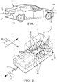
- Fig. 1 illustrates a non-limiting example of an automated vehicle 120 equipped with a plurality of signaling-devices 122.
- the term automated vehicle covers a wide range of degrees or levels of automation including instances when the automated vehicle 120 is being operated in an fully-automated or autonomous mode, where a human-operator (not shown) of the automated vehicle 120 may do little more than designate a destination in order to operate the automated vehicle 120.
- teachings presented herein are useful when the automated vehicle 120 is operated in a manual-mode where the degree or level of automation may be little more than activating a warning indicator (visible and/or audible) to assist the human-operator as needed to change lanes and/or avoid interference with and/or a collision with, for example, another vehicle.
- a warning indicator visible and/or audible
- the signaling-devices 122 may be configured as radar-sensors useful for detecting objects in a vicinity of the automated vehicle 120 based on radar-signals 124 transmitted by the signaling-devices 122. Such signaling-devices 122 may also be useful for parking assistance, collision avoidance, and other object detection functions.
- Fig. 2 illustrates a non-limiting example of a ball-grid-array attached radio-frequency integrated-circuit printed-circuit-board assembly 10, hereafter the assembly 10, which may be part of one or more instances of the signaling-devices 122.
- the assembly 10 is configured to propagate a radio-frequency signal, hereafter the signal 12, from a die 14 (i.e. integrated circuit) toward an antenna (not shown).
- the design of the assembly 10 provides for sufficient reliability such that the assembly 10 will be suitable for use on the automated vehicle 120.
- the die 14 includes a signal-out-pad 16 and a plurality of ground-pads 18 arranged about the signal-out-pad 16. While this non-limiting example has all of the pads except the signal-out-pad 16 identified as ground-pads, those in the art will recognize that there will be additional pads for other signals and power. Indeed, there may be several hundred pads and corresponding solder-balls on a complex ball-grid-array (BGA) attached integrated circuit. Only a small section germane to, for example, microwave operation, a limited number of pads and solder-balls are shown only in order to simplify the drawings.
- BGA ball-grid-array
- the die 14 is generally operable to output a signal via the signal-out-pad 16, where the signal may be characterized by a frequency, for example seventy-seven Giga-Hertz (77GHz) for example if the signaling-devices 122 are radar-sensors.
- 77GHz seventy-seven Giga-Hertz
- the assembly 10 includes a plurality of solder-balls 20 used to attach the die to a printed-circuit-board 22, hereafter the PCB 22.
- solder-balls 20 used to attach the die to a printed-circuit-board 22, hereafter the PCB 22.
- a variety of formulations of commercially available solder-balls are known to those skilled in the art.
- the solder-balls are attached to the die 14 prior to aligning and placing the die 14 with solder-balls onto corresponding instances of solder-pads 24 ( Fig. 3 ) on the PCB 22, and then the assembly 10 is heated sufficiently to melt or reflow the plurality of solder-balls 20 and thereby solder the die 14 to the PCB 22.
- the PCB 22 includes a substrate 26 that defines a plane 30 parallel to the x-axis and the y-axis illustrated in Fig. 2 .
- the substrate 26 is formed from any of many suitable, commercially available materials, as will be recognized by those in the art.
- the substrate 26 includes a plurality of vias 28 oriented normal to the plane 30 (i.e. parallel to the z-axis) and extending from a top-side 32 ( Fig. 4 ) of the substrate 26 to a bottom-side 34 of the substrate 26.
- the plurality of vias 28 are characterized by a via-height 36 that corresponds to (i.e. is equal to or is essentially equal to) the thickness of the substrate 26.
- Each of the plurality of vias 28 is preferably a conductive element comparable to a plated-through-hole or plated-via, which are known to those in the PCB arts.
- the plurality of vias 28 may be filled with conductive or non-conductive material, if desired.
- Figs. 3 and 4 show additional non-limiting details of the PCB 22 which includes a top-metal layer 38 attached to the top-side 32 of the substrate 26.
- the top-metal layer 38 in cooperation with a solder-mask 48 that overlies part of the top-metal layer 38 is configured to provide solder-pads 24 for the plurality of solder-balls 20 to attach the die 14 to the top-metal layer 38.
- the PCB 22 also includes a bottom-metal 44 layer attached to the bottom-side 34 of the substrate 26.
- a suitable example of laminate/prepreg that can be purchased with the top-metal layer 38 and the bottom-metal layer 44 already attached to the substrate 26 is model IT-150DA from ITEQ® with a thickness of 0.5mm, a dielectric constant (Dk) of 3.5, and a lost-tangent (tand) of 0.005.
- the plurality of vias 28 may be drilled through the purchase laminate and then a subsequent plating process can be used to plate each of the plurality of vias 28 and thereby electrically connect (direct-current wise) the top-metal layer 38 to the bottom-metal layer 44.
- the top-metal layer 38, the plurality of vias 28 through the substrate 26, and the bottom-metal layer 44 then cooperate to form a substrate-integrated-waveguide 50, hereafter referred to as the SIW 50, suitable to propagate the signal 12 in a direction 46 parallel to the plane 30 of the substrate 26.
- suitable dimensions for the plurality of vias 28 include a via-diameter of 0.25mm and a via-spacing or via-pitch of 0.45mm.
- the PCB 22 may advantageously include a solder-mask 48 overlaying at least the portion of the top-metal layer 38 underneath the die 14. That is, the solder-mask 48 may be used to define the locations of the solder-pads 24 on top of a contiguous or continuous region of the top-metal layer 38. While the solder-mask 48 is shown as only extending to the boundaries of the die 14, this is not a requirement. The solder-mask 48 could be extended to cover the entirety of the top-metal layer 38 with little effect on performance.
- Solder-mask could also be applied over the bottom metal layer if desired which could provide some environmental protection to the metal forming the bottom-metal layer 44, and potentially reduce self-bending of the PCB 22 during temperature cycling if the top-metal layer 38 is also entirely covered by the solder-mask 48.
- the top-metal layer 38 is configured to define a U-shaped-slot 52 between a signal-portion 54 of the top-metal layer 38 aligned with the signal-out-pad 16 and the SIW 50, and a ground-portion 56 of the top-metal layer 38 aligned with the plurality of ground-pads 18.
- the U-shaped-slot 52 may be formed in the top-metal layer 38 using well-known photo-etching processes.
- the U-shaped-slot 52 is provided so a voltage at the signal-out-pad 16 that is fluctuating relative to the plurality of ground-pads 18 will cause an alternating electric field to form across the U-shaped-slot 52 and thereby project or emit RF energy into the SIW 50.
- the U-shaped-slot 52 characterized by a slot-length 58 that is selected based on the frequency of the signal 12, 3.2mm for example for 77GHz and a shape-width 60.
- the U-shaped-slot 52 is also characterized by a slot-width 64 that is selected, at least in part, based on the via-height 36.
- the shape-width 60 influences how well or how efficiently energy from the electric field directed across the U-shaped-slot 52 is propagated from the signal-portion 54 of the top-metal layer 38 into the substrate-integrated-waveguide, i.e. the SIW 50. It is recognized that it is preferable to make the slot-width 64 as small as possible, but the minimum dimension is determined by the capability of the photo-etching process. It is also recognized that the greater the value of a ratio defined by the via-height 36 divided by the slot-width 64, the better the coupling of RF energy into the SIW 50.
- a relatively inexpensive photo-etching process is expected to provide a reliable and well-defined instance of the U-shaped-slot 52 if the slot-width 64 is 0.1mm. It is also believed that the minimum value of the above defined ratio should be greater than three (3), so a minimum recommended value of the via-height 36 is 0.3mm. Since substrates with thickness of 0.5mm are readily available and reasonably durable, 0.5mm is the suggested value for the via-height 36.
- the signal-portion 54 and the ground-portion 56 are considered to cooperate to form a planar-waveguide that transfers the signal 12 from the die 14 directly into the substrate-integrated-waveguide (the SIW 50).
- the use of 'directly' means that no intermediate microwave components are present in the signal path between the solder-ball attached to the signal-portion 54 and the SIW 50.
- the plurality of ground-pads 18 is arranged about the signal-out-pad 16 is arranged such that solder-balls 20 attached to the plurality of ground-pads 18 form a shield 62 used to reduce leakage of the signal 12 radiated from a solder-ball 20 attached to the signal-out-pad 16.
- the U-shape of the shield 62 in this example is selected because of the close proximity of the signal-out-pad 16 to the edge of the die 14. If the die 14 were illustrated to be substantially larger with many more solder-pads and solder-balls, it is contemplated that the ground-pads and associated solder-balls could be arranged into multiple concentric rings if leakage were a particular problem.
- a ball-grid-array attached radio-frequency integrated-circuit printed-circuit-board assembly (the assembly 10) is provided.
- the design configuration described herein was validated by measurement.
- innovative features include: direct connection of signal-out pad 16 to SIW 50; transitions from the die 14 to an intermediate component such as a microstrip and from the intermediate component to SIW 50 are eliminated; the radiating structure of the U-shaped-slot 52 is implemented using standard planar printed circuit board technology; no external components or special processes are required; and compensation for die output impedance or circuit discontinuities (matching) is provided by adjusting U-shaped-slot size and position.
Landscapes
- Engineering & Computer Science (AREA)
- Microelectronics & Electronic Packaging (AREA)
- Physics & Mathematics (AREA)
- Electromagnetism (AREA)
- Structure Of Printed Boards (AREA)
- Geometry (AREA)
- Radar Systems Or Details Thereof (AREA)
- Combinations Of Printed Boards (AREA)
Abstract
Description
- This disclosure generally relates to a BGA circuit assembly, and more particularly relates to using a U-shaped-slot in a top-metal layer to generate an electric field directed across the U-shaped-slot whereby a signal is propagated from the U-shaped-slot directly into the substrate-integrated-waveguide (SIW).
- It is known to equip automated vehicles with a wide variety of sensing systems. Various sensor configurations have been developed to provide assistance or information to a driver or autonomous controller regarding the environment surrounding the vehicle. Advances in radio frequency signaling technology have enabled the development of sophisticated system-on-a-chip integrated circuits. The functionality required for environmental sensing or communications can be embodied in integrated circuit components. Example uses for such devices include automotive vehicle radar detection systems, robotics guiding systems, and Wi-Fi data transfer.
- Antennas for radio-frequency (RF) signal transmission vary depending on the particular sensing or communication of interest. For example, relatively small, low-gain, broadband antennas are used for Wi-Fi communications, and relatively large, high-gain antennas are typically used for point-to-point data communications. Antennas useful for automotive radar systems typically fall between those two extremes. One type of antenna component that can be useful for propagating RF signals in a vehicle-based radar system is known as a substrate-integrated-waveguide (SIW). The SIW is desirable because of high-efficiency and are relatively low-cost.
- One challenge associated with utilizing SIWs in a vehicle-based sensing or communication system is associated with the connection between an integrated circuit and the SIW. For example, microstrip or coplanar waveguide microwave transmission lines can provide an interface between the integrated circuit and the SIW. However, such connections include drawbacks, such as the requirement for a microwave component that matches the field configuration peculiar to each transmission line. The transition associated with such a microwave component increases microwave loss and introduces microwave reflections that may limit bandwidth and impact the ability to produce such systems. When a microstrip is used, bandwidth may be limited by the requirement for the ground connection to pass from the integrated circuit component connectors through the SIW substrate to a metal layer on that substrate. Furthermore, such connections are typically made using a relatively expensive blind via process.
- Described herein is a high-frequency circuit-board-assembly that includes a means to form a direct connection of ball-grid-array attached radio-frequency integrated-circuit output to substrate-integrated-waveguide (SIW) formed by features on a printed-circuit-board (PCB). The assembly overcomes the problems described above by eliminating various interconnecting transitions such as microstrips, which maximizes performance while minimizing complexity. The direct connection allows for radio-frequency (RF) energy from the integrated circuit to be radiated directly into a SIW by or through a U-shaped-slot etched in the top-metal layer of the PCB. The resonant frequency of the U-shaped-slot is determined or influenced by a slot-length of the U, where the length is the totality of the perimeter of the U. That is, when viewing the U on this page, the length is the sum of twice the distance measured in an up-down direction plus one of the distance measured in a left-right direction of the U. The efficiency of coupling of RF energy from the U-shaped-slot is determined or influenced by a shape-width corresponding to the width of the base of the U-shaped-slot. That is, the shape-width is measured in a left-right direction across the U on this page. Some of the vias used to form the SIW are also used to form a back-short that helps to direct or reflect RF energy toward a desired direction of propagation of the SIW.
- In accordance with one embodiment, a ball-grid-array attached radio-frequency integrated-circuit printed-circuit-board assembly is provided. The assembly includes a die, a plurality of solder-balls, a substrate, a top-metal layer, and a bottom-metal layer. The die includes a signal-out-pad and a plurality of ground-pads arranged about the signal-out-pad. The die is operable to output a signal via the signal-out-pad. The signal characterized by a frequency. The plurality of solder-balls is used to attach the die. The substrate defines a plane and includes a plurality of vias oriented normal to the plane and extending from a top-side of the substrate to a bottom-side of the substrate. The plurality of vias is characterized by a via-height that corresponds to a thickness of the substrate. The top-metal layer is attached to the top-side of the substrate. The top-metal layer is configured to provide solder-pads for the plurality of solder-balls to attach the die to the top-metal layer. The bottom-metal layer is attached to the bottom-side of the substrate. The top-metal layer, the plurality of vias in the substrate, and the bottom-metal layer cooperate to form a substrate-integrated-waveguide suitable to propagate the signal in a direction parallel to the plane of the substrate. The top-metal layer is configured to define a U-shaped-slot between a signal-portion of the top-metal layer aligned with the signal-out-pad and the substrate-integrated-waveguide, and a ground-portion of the top-metal layer aligned with the plurality of ground-pads. The U-shaped-slot is characterized by a slot-length that is selected based on the frequency of the signal, and a slot-width that is selected based on the via-height such that the signal generates an electric field directed across the U-shaped-slot whereby the signal is propagated from the signal-portion of the top-metal layer into the substrate-integrated-waveguide.
- The signal-portion and the ground-portion may cooperate to form a planar-waveguide that transfers the signal from the die directly into the substrate-integrated-waveguide. The plurality of ground-pads arranged about the signal-out-pad may be arranged such that solder-balls attached to the plurality of ground-pads form a shield used to reduce leakage of the signal radiated from a solder-ball attached to the signal-out-pad. A ratio defined by the via-height divided by the slot-width may be greater than three.
- Further features and advantages will appear more clearly on a reading of the following detailed description of the preferred embodiment, which is given by way of non-limiting example only and with reference to the accompanying drawings.
- The present invention will now be described, by way of example with reference to the accompanying drawings, in which:
-
Fig. 1 is an automated vehicle equipped with a sensing-device in accordance with one embodiment; -
Fig. 2 is an isometric view of a circuit assembly used in the sensing-device ofFig. 1 in accordance with one embodiment; -
Fig. 3 is a top view of a printed-circuit-board used in circuit assembly ofFig. 2 in accordance with one embodiment; and -
Fig. 4 is a side view of a partial assembly of the circuit assembly ofFig. 2 in accordance with one embodiment. - Embodiments of this invention provide a signaling device with an improved connection between a ball-grid-array attached integrated-circuit die and a substrate-integrated-waveguide (SIW). Embodiments of this invention advantageously eliminate interconnecting transitions between the die the SIW, which maximizes system performance while minimizing complexity.
-
Fig. 1 illustrates a non-limiting example of anautomated vehicle 120 equipped with a plurality of signaling-devices 122. As used herein, the term automated vehicle covers a wide range of degrees or levels of automation including instances when theautomated vehicle 120 is being operated in an fully-automated or autonomous mode, where a human-operator (not shown) of theautomated vehicle 120 may do little more than designate a destination in order to operate theautomated vehicle 120. It is also contemplated that the teachings presented herein are useful when theautomated vehicle 120 is operated in a manual-mode where the degree or level of automation may be little more than activating a warning indicator (visible and/or audible) to assist the human-operator as needed to change lanes and/or avoid interference with and/or a collision with, for example, another vehicle. - By way of example, the signaling-
devices 122 may be configured as radar-sensors useful for detecting objects in a vicinity of theautomated vehicle 120 based on radar-signals 124 transmitted by the signaling-devices 122. Such signaling-devices 122 may also be useful for parking assistance, collision avoidance, and other object detection functions. -
Fig. 2 illustrates a non-limiting example of a ball-grid-array attached radio-frequency integrated-circuit printed-circuit-board assembly 10, hereafter theassembly 10, which may be part of one or more instances of the signaling-devices 122. In general, theassembly 10 is configured to propagate a radio-frequency signal, hereafter thesignal 12, from a die 14 (i.e. integrated circuit) toward an antenna (not shown). The design of theassembly 10 provides for sufficient reliability such that theassembly 10 will be suitable for use on theautomated vehicle 120. - The die 14 includes a signal-out-
pad 16 and a plurality of ground-pads 18 arranged about the signal-out-pad 16. While this non-limiting example has all of the pads except the signal-out-pad 16 identified as ground-pads, those in the art will recognize that there will be additional pads for other signals and power. Indeed, there may be several hundred pads and corresponding solder-balls on a complex ball-grid-array (BGA) attached integrated circuit. Only a small section germane to, for example, microwave operation, a limited number of pads and solder-balls are shown only in order to simplify the drawings. Thedie 14 is generally operable to output a signal via the signal-out-pad 16, where the signal may be characterized by a frequency, for example seventy-seven Giga-Hertz (77GHz) for example if the signaling-devices 122 are radar-sensors. - The
assembly 10 includes a plurality of solder-balls 20 used to attach the die to a printed-circuit-board 22, hereafter thePCB 22. A variety of formulations of commercially available solder-balls are known to those skilled in the art. Typically, the solder-balls are attached to the die 14 prior to aligning and placing the die 14 with solder-balls onto corresponding instances of solder-pads 24 (Fig. 3 ) on thePCB 22, and then theassembly 10 is heated sufficiently to melt or reflow the plurality of solder-balls 20 and thereby solder the die 14 to thePCB 22. - The
PCB 22 includes asubstrate 26 that defines aplane 30 parallel to the x-axis and the y-axis illustrated inFig. 2 . Thesubstrate 26 is formed from any of many suitable, commercially available materials, as will be recognized by those in the art. Thesubstrate 26 includes a plurality ofvias 28 oriented normal to the plane 30 (i.e. parallel to the z-axis) and extending from a top-side 32 (Fig. 4 ) of thesubstrate 26 to a bottom-side 34 of thesubstrate 26. The plurality ofvias 28 are characterized by a via-height 36 that corresponds to (i.e. is equal to or is essentially equal to) the thickness of thesubstrate 26. Each of the plurality ofvias 28 is preferably a conductive element comparable to a plated-through-hole or plated-via, which are known to those in the PCB arts. The plurality ofvias 28 may be filled with conductive or non-conductive material, if desired. -
Figs. 3 and 4 show additional non-limiting details of thePCB 22 which includes a top-metal layer 38 attached to the top-side 32 of thesubstrate 26. The top-metal layer 38 in cooperation with a solder-mask 48 that overlies part of the top-metal layer 38 is configured to provide solder-pads 24 for the plurality of solder-balls 20 to attach the die 14 to the top-metal layer 38. ThePCB 22 also includes a bottom-metal 44 layer attached to the bottom-side 34 of thesubstrate 26. A suitable example of laminate/prepreg that can be purchased with the top-metal layer 38 and the bottom-metal layer 44 already attached to thesubstrate 26 is model IT-150DA from ITEQ® with a thickness of 0.5mm, a dielectric constant (Dk) of 3.5, and a lost-tangent (tand) of 0.005. - The plurality of
vias 28 may be drilled through the purchase laminate and then a subsequent plating process can be used to plate each of the plurality ofvias 28 and thereby electrically connect (direct-current wise) the top-metal layer 38 to the bottom-metal layer 44. As will be recognized by those in the art, the top-metal layer 38, the plurality ofvias 28 through thesubstrate 26, and the bottom-metal layer 44 then cooperate to form a substrate-integrated-waveguide 50, hereafter referred to as theSIW 50, suitable to propagate thesignal 12 in adirection 46 parallel to theplane 30 of thesubstrate 26. If thesignal 12 has a frequency of 77GHz, suitable dimensions for the plurality ofvias 28 include a via-diameter of 0.25mm and a via-spacing or via-pitch of 0.45mm. - In order to constrain the solder of the solder-
balls 20 during reflow, and help align the die 14 to thePCB 22, thePCB 22 may advantageously include a solder-mask 48 overlaying at least the portion of the top-metal layer 38 underneath thedie 14. That is, the solder-mask 48 may be used to define the locations of the solder-pads 24 on top of a contiguous or continuous region of the top-metal layer 38. While the solder-mask 48 is shown as only extending to the boundaries of the die 14, this is not a requirement. The solder-mask 48 could be extended to cover the entirety of the top-metal layer 38 with little effect on performance. Solder-mask could also be applied over the bottom metal layer if desired which could provide some environmental protection to the metal forming the bottom-metal layer 44, and potentially reduce self-bending of thePCB 22 during temperature cycling if the top-metal layer 38 is also entirely covered by the solder-mask 48. - In order to couple the
signal 12 from the signal-out pad 16 of the die 14 directly into theSIW 50, the top-metal layer 38 is configured to define a U-shaped-slot 52 between a signal-portion 54 of the top-metal layer 38 aligned with the signal-out-pad 16 and theSIW 50, and a ground-portion 56 of the top-metal layer 38 aligned with the plurality of ground-pads 18. The U-shaped-slot 52 may be formed in the top-metal layer 38 using well-known photo-etching processes. The U-shaped-slot 52 is provided so a voltage at the signal-out-pad 16 that is fluctuating relative to the plurality of ground-pads 18 will cause an alternating electric field to form across the U-shaped-slot 52 and thereby project or emit RF energy into theSIW 50. The U-shaped-slot 52 characterized by a slot-length 58 that is selected based on the frequency of thesignal 12, 3.2mm for example for 77GHz and a shape-width 60. The U-shaped-slot 52 is also characterized by a slot-width 64 that is selected, at least in part, based on the via-height 36. The shape-width 60 influences how well or how efficiently energy from the electric field directed across the U-shaped-slot 52 is propagated from the signal-portion 54 of the top-metal layer 38 into the substrate-integrated-waveguide, i.e. theSIW 50. It is recognized that it is preferable to make the slot-width 64 as small as possible, but the minimum dimension is determined by the capability of the photo-etching process. It is also recognized that the greater the value of a ratio defined by the via-height 36 divided by the slot-width 64, the better the coupling of RF energy into theSIW 50. By way of example and not limitation, a relatively inexpensive photo-etching process is expected to provide a reliable and well-defined instance of the U-shaped-slot 52 if the slot-width 64 is 0.1mm. It is also believed that the minimum value of the above defined ratio should be greater than three (3), so a minimum recommended value of the via-height 36 is 0.3mm. Since substrates with thickness of 0.5mm are readily available and reasonably durable, 0.5mm is the suggested value for the via-height 36. - By way of further explanation and not limitation, the signal-
portion 54 and the ground-portion 56 are considered to cooperate to form a planar-waveguide that transfers thesignal 12 from the die 14 directly into the substrate-integrated-waveguide (the SIW 50). As used herein the use of 'directly' means that no intermediate microwave components are present in the signal path between the solder-ball attached to the signal-portion 54 and theSIW 50. - The plurality of ground-
pads 18 is arranged about the signal-out-pad 16 is arranged such that solder-balls 20 attached to the plurality of ground-pads 18 form ashield 62 used to reduce leakage of thesignal 12 radiated from a solder-ball 20 attached to the signal-out-pad 16. The U-shape of theshield 62 in this example is selected because of the close proximity of the signal-out-pad 16 to the edge of thedie 14. If the die 14 were illustrated to be substantially larger with many more solder-pads and solder-balls, it is contemplated that the ground-pads and associated solder-balls could be arranged into multiple concentric rings if leakage were a particular problem. - Accordingly, a ball-grid-array attached radio-frequency integrated-circuit printed-circuit-board assembly (the assembly 10) is provided. The design configuration described herein was validated by measurement. Innovative features include: direct connection of signal-
out pad 16 to SIW 50; transitions from the die 14 to an intermediate component such as a microstrip and from the intermediate component to SIW 50 are eliminated; the radiating structure of the U-shaped-slot 52 is implemented using standard planar printed circuit board technology; no external components or special processes are required; and compensation for die output impedance or circuit discontinuities (matching) is provided by adjusting U-shaped-slot size and position. - While this invention has been described in terms of the preferred embodiments thereof, it is not intended to be so limited, but rather only to the extent set forth in the claims that follow.
Claims (4)
- A ball-grid-array attached radio-frequency integrated-circuit printed-circuit-board assembly (10) configured to propagate a radio-frequency signal (12) and suitable for use in an automated vehicle (120), said assembly (10) comprising:a die (14) that includes a signal-out-pad (16) and a plurality of ground-pads (18) arranged about the signal-out-pad (16), said die (14) operable to output a signal (12) via the signal-out-pad (16), said signal (12) characterized by a frequency;a plurality of solder-balls (20) used to attach the die (14);a substrate (26) that defines a plane (30) and includes a plurality of vias (28) oriented normal to the plane (30) and extending from a top-side (32) of the substrate (26) to a bottom-side (34) of the substrate (26), wherein the plurality of vias (28) are characterized by a via-height (36) that corresponds to a thickness of the substrate (26);a top-metal layer (38) attached to the top-side (32) of the substrate (26), said top-metal layer (38) configured to provide solder-pads (24) for the plurality of solder-balls (20) to attach the die (14) to the top-metal layer (38); anda bottom-metal layer (44) attached to the bottom-side (34) of the substrate (26), wherein the top-metal layer (38), the plurality of vias (28) through the substrate (26), and the bottom-metal layer (44) cooperate to form a substrate-integrated-waveguide (50) suitable to propagate the signal (12) in a direction (46) parallel to the plane (30) of the substrate (26),wherein the top-metal layer (38) is configured to define a u-shaped-slot (52) between a signal-portion (54) of the top-metal layer (38) aligned with the signal-out-pad (16) and the substrate-integrated-waveguide (50), and a ground-portion (56) of the top-metal layer (38) aligned with the plurality of ground-pads (18), said u-shaped-slot (52) characterized by a slot-length (58) that is selected based on the frequency of the signal (12), and a slot-width (64) that is selected based on the via-height (36) such that the signal (12) generates an electric field directed across the u-shaped-slot (52) whereby the signal (12) is propagated from the signal-portion (54) of the top-metal layer (38) into the substrate-integrated-waveguide (50).
- The assembly (10) in accordance with claim 1, wherein the signal-portion (54) and the ground-portion (56) cooperate to form a planar-waveguide that transfers the signal (12) from the die (14) directly into the substrate-integrated-waveguide (50).
- The assembly (10) according to any one of the preceding claims, wherein the plurality of ground-pads (18) arranged about the signal-out-pad (16) is arranged such that solder-balls (20) attached to the plurality of ground-pads (18) form a shield (62) used to reduce leakage of the signal (12) radiated from a solder-ball (20) attached to the signal-out-pad (16).
- The assembly (10) according to any one of the preceding claims, wherein a ratio defined by the via-height (36) divided by the slot-width (64) is greater than three (3).
Applications Claiming Priority (1)
| Application Number | Priority Date | Filing Date | Title |
|---|---|---|---|
| US15/292,824 US10199707B2 (en) | 2016-10-13 | 2016-10-13 | Ball-grid-array radio-frequency integrated-circuit printed-circuit-board assembly for automated vehicles |
Publications (2)
| Publication Number | Publication Date |
|---|---|
| EP3309896A1 true EP3309896A1 (en) | 2018-04-18 |
| EP3309896B1 EP3309896B1 (en) | 2022-04-06 |
Family
ID=60080589
Family Applications (1)
| Application Number | Title | Priority Date | Filing Date |
|---|---|---|---|
| EP17194590.0A Active EP3309896B1 (en) | 2016-10-13 | 2017-10-03 | Ball-grid-array radio-frequency integrated-circuit printed-circuit-board assembly for automated vehicles |
Country Status (3)
| Country | Link |
|---|---|
| US (1) | US10199707B2 (en) |
| EP (1) | EP3309896B1 (en) |
| CN (1) | CN107946278B (en) |
Cited By (2)
| Publication number | Priority date | Publication date | Assignee | Title |
|---|---|---|---|---|
| EP3706236A1 (en) * | 2019-03-07 | 2020-09-09 | Aptiv Technologies Limited | Signaling device including a slot transition between a substrate integrated waveguide and a signal generator |
| CN113169434A (en) * | 2018-12-04 | 2021-07-23 | 三菱电机株式会社 | Waveguide tube planar line converter and high-frequency module |
Families Citing this family (13)
| Publication number | Priority date | Publication date | Assignee | Title |
|---|---|---|---|---|
| US10468738B2 (en) * | 2016-03-15 | 2019-11-05 | Aptiv Technologies Limited | Signaling device including a substrate integrated waveguide coupled to a signal generator through a ball grid array |
| US11183751B2 (en) * | 2017-09-20 | 2021-11-23 | Aptiv Technologies Limited | Antenna device with direct differential input useable on an automated vehicle |
| CN110868793B (en) * | 2019-11-22 | 2025-08-08 | 中国电子科技集团公司第十三研究所 | Shielding structure and three-dimensional integrated microwave circuit |
| EP4016620A1 (en) | 2020-12-16 | 2022-06-22 | Nxp B.V. | Package with an integrated circuit die and a waveguide launcher |
| US12055654B2 (en) * | 2021-08-20 | 2024-08-06 | Gm Cruise Holdings Llc | Scanning radar system with substrate integrated waveguides and heat dissipating structures |
| TWI835035B (en) * | 2021-12-09 | 2024-03-11 | 高技企業股份有限公司 | Circuit board and eletronic package using the same |
| US12613334B2 (en) * | 2022-06-28 | 2026-04-28 | Magna Electronics, Llc | Integrated circuit to waveguide transitional structures and related sensor assemblies |
| CN115551183B (en) * | 2022-09-29 | 2026-04-10 | 超聚变数字技术股份有限公司 | Circuit boards and electronic devices |
| US12548877B2 (en) | 2022-10-05 | 2026-02-10 | Nxp B.V. | Printed circuit board (PCB) including a vertical launcher having a signal via for radiating signal energy through a PCB channel region |
| US12451579B2 (en) | 2022-12-30 | 2025-10-21 | Nxp B.V. | Interposers with millimeter-wave transitions |
| US12451578B2 (en) | 2022-12-30 | 2025-10-21 | Nxp B.V. | Interposers with millimeter-wave coaxial-to-waveguide transistions |
| CN116190336B (en) * | 2023-02-15 | 2026-02-03 | 湖北九峰山实验室 | Radio frequency integrated equipment and preparation method thereof |
| CN116454622A (en) * | 2023-04-06 | 2023-07-18 | 北京理工大学重庆创新中心 | Substrate integrated waveguide coupling feed structure of spherical pin grid array |
Citations (3)
| Publication number | Priority date | Publication date | Assignee | Title |
|---|---|---|---|---|
| JP3852598B2 (en) * | 2001-03-19 | 2006-11-29 | 宇部興産株式会社 | Dielectric filter and duplexer |
| EP2337147A1 (en) * | 2009-12-14 | 2011-06-22 | Fujitsu Limited | Signal converter and high-frequency circuit module |
| GB2499792A (en) * | 2012-02-28 | 2013-09-04 | Canon Kk | Electronic device comprising an electronic die, a substrate integrated waveguide (SIW) and a flip-chip ball grid array package |
Family Cites Families (4)
| Publication number | Priority date | Publication date | Assignee | Title |
|---|---|---|---|---|
| CN203826522U (en) * | 2014-04-18 | 2014-09-10 | 华南理工大学 | Broadband substrate integrated waveguide filter adopting U-shaped slot line |
| KR101621480B1 (en) | 2014-10-16 | 2016-05-16 | 현대모비스 주식회사 | Transit structure of waveguide and dielectric waveguide |
| US9537199B2 (en) * | 2015-03-19 | 2017-01-03 | International Business Machines Corporation | Package structure having an integrated waveguide configured to communicate between first and second integrated circuit chips |
| US10109910B2 (en) * | 2016-05-26 | 2018-10-23 | Delphi Technologies, Inc. | Antenna device with accurate beam elevation control useable on an automated vehicle |
-
2016
- 2016-10-13 US US15/292,824 patent/US10199707B2/en active Active
-
2017
- 2017-10-03 EP EP17194590.0A patent/EP3309896B1/en active Active
- 2017-10-12 CN CN201710947219.6A patent/CN107946278B/en active Active
Patent Citations (3)
| Publication number | Priority date | Publication date | Assignee | Title |
|---|---|---|---|---|
| JP3852598B2 (en) * | 2001-03-19 | 2006-11-29 | 宇部興産株式会社 | Dielectric filter and duplexer |
| EP2337147A1 (en) * | 2009-12-14 | 2011-06-22 | Fujitsu Limited | Signal converter and high-frequency circuit module |
| GB2499792A (en) * | 2012-02-28 | 2013-09-04 | Canon Kk | Electronic device comprising an electronic die, a substrate integrated waveguide (SIW) and a flip-chip ball grid array package |
Cited By (4)
| Publication number | Priority date | Publication date | Assignee | Title |
|---|---|---|---|---|
| CN113169434A (en) * | 2018-12-04 | 2021-07-23 | 三菱电机株式会社 | Waveguide tube planar line converter and high-frequency module |
| CN113169434B (en) * | 2018-12-04 | 2022-07-01 | 三菱电机株式会社 | Waveguide tube planar line converter and high-frequency module |
| EP3706236A1 (en) * | 2019-03-07 | 2020-09-09 | Aptiv Technologies Limited | Signaling device including a slot transition between a substrate integrated waveguide and a signal generator |
| US11139581B2 (en) | 2019-03-07 | 2021-10-05 | Aptiv Technologies Limited | Signaling device including a slot transition between a substrate integrated waveguide and a signal generator |
Also Published As
| Publication number | Publication date |
|---|---|
| CN107946278B (en) | 2020-08-14 |
| EP3309896B1 (en) | 2022-04-06 |
| US10199707B2 (en) | 2019-02-05 |
| CN107946278A (en) | 2018-04-20 |
| US20180108968A1 (en) | 2018-04-19 |
Similar Documents
| Publication | Publication Date | Title |
|---|---|---|
| US10199707B2 (en) | Ball-grid-array radio-frequency integrated-circuit printed-circuit-board assembly for automated vehicles | |
| EP3460903B1 (en) | Antenna device with direct differential input useable on an automated vehicle | |
| US11145961B2 (en) | Vehicle radar signaling device including a substrate integrated waveguide | |
| CN111758044B (en) | Radar system with plastic antenna for detecting the surroundings of a motor vehicle | |
| JP5167709B2 (en) | Wireless IC device, inspection system thereof, and method of manufacturing wireless IC device using the inspection system | |
| EP1443599B1 (en) | Printed circuit board dipole antenna structure with impedance matching trace | |
| CN104051440B (en) | Semiconductor structure with antenna | |
| KR101621480B1 (en) | Transit structure of waveguide and dielectric waveguide | |
| EP1777551A2 (en) | Millimeter-wave radar apparatus and millimeter radar system | |
| US10141636B2 (en) | Volumetric scan automotive radar with end-fire antenna on partially laminated multi-layer PCB | |
| US20100141350A1 (en) | High-Frequency Circuit Board, High-Frequency Circuit Module, and Radar Apparatus | |
| EP1724714A2 (en) | Patch antenna for RFID tag | |
| JP2006042059A (en) | Radio communication apparatus and impedance controlling method thereof | |
| US20200217922A1 (en) | Electronic component for emitting and receiving radar signals | |
| CN116581520A (en) | Antenna arrangement, radar sensor arrangement and method for producing the antenna arrangement | |
| CN217306728U (en) | Power divider, antenna device, radio device, and apparatus | |
| CN119223397A (en) | Radar measuring device for detecting fill levels and distances | |
| JP3950133B2 (en) | High frequency circuit board | |
| CN107210523A (en) | Circuit board and the electronic installation with the circuit board | |
| CN218334344U (en) | Array Antennas, Radios and Electronics | |
| US20070139290A1 (en) | RFID tag and RFID system having the same | |
| US20230163438A1 (en) | Signal transmission system and dielectric waveguide | |
| CN113938139A (en) | Signal receiving, signal transmitting chain, radio device and feeder line setting method | |
| CN117117483A (en) | Antenna structures, millimeter wave radar and mobile devices |
Legal Events
| Date | Code | Title | Description |
|---|---|---|---|
| PUAI | Public reference made under article 153(3) epc to a published international application that has entered the european phase |
Free format text: ORIGINAL CODE: 0009012 |
|
| STAA | Information on the status of an ep patent application or granted ep patent |
Free format text: STATUS: THE APPLICATION HAS BEEN PUBLISHED |
|
| AK | Designated contracting states |
Kind code of ref document: A1 Designated state(s): AL AT BE BG CH CY CZ DE DK EE ES FI FR GB GR HR HU IE IS IT LI LT LU LV MC MK MT NL NO PL PT RO RS SE SI SK SM TR |
|
| AX | Request for extension of the european patent |
Extension state: BA ME |
|
| STAA | Information on the status of an ep patent application or granted ep patent |
Free format text: STATUS: REQUEST FOR EXAMINATION WAS MADE |
|
| 17P | Request for examination filed |
Effective date: 20181018 |
|
| RBV | Designated contracting states (corrected) |
Designated state(s): AL AT BE BG CH CY CZ DE DK EE ES FI FR GB GR HR HU IE IS IT LI LT LU LV MC MK MT NL NO PL PT RO RS SE SI SK SM TR |
|
| RAP1 | Party data changed (applicant data changed or rights of an application transferred) |
Owner name: APTIV TECHNOLOGIES LIMITED |
|
| STAA | Information on the status of an ep patent application or granted ep patent |
Free format text: STATUS: EXAMINATION IS IN PROGRESS |
|
| 17Q | First examination report despatched |
Effective date: 20190222 |
|
| REG | Reference to a national code |
Ref country code: DE Ref legal event code: R079 Ref document number: 602017055465 Country of ref document: DE Free format text: PREVIOUS MAIN CLASS: H01P0003120000 Ipc: H01P0005107000 |
|
| GRAP | Despatch of communication of intention to grant a patent |
Free format text: ORIGINAL CODE: EPIDOSNIGR1 |
|
| STAA | Information on the status of an ep patent application or granted ep patent |
Free format text: STATUS: GRANT OF PATENT IS INTENDED |
|
| RIC1 | Information provided on ipc code assigned before grant |
Ipc: H01P 5/107 20060101AFI20191217BHEP |
|
| INTG | Intention to grant announced |
Effective date: 20200110 |
|
| GRAJ | Information related to disapproval of communication of intention to grant by the applicant or resumption of examination proceedings by the epo deleted |
Free format text: ORIGINAL CODE: EPIDOSDIGR1 |
|
| STAA | Information on the status of an ep patent application or granted ep patent |
Free format text: STATUS: EXAMINATION IS IN PROGRESS |
|
| INTC | Intention to grant announced (deleted) | ||
| GRAP | Despatch of communication of intention to grant a patent |
Free format text: ORIGINAL CODE: EPIDOSNIGR1 |
|
| STAA | Information on the status of an ep patent application or granted ep patent |
Free format text: STATUS: GRANT OF PATENT IS INTENDED |
|
| INTG | Intention to grant announced |
Effective date: 20211012 |
|
| GRAS | Grant fee paid |
Free format text: ORIGINAL CODE: EPIDOSNIGR3 |
|
| GRAA | (expected) grant |
Free format text: ORIGINAL CODE: 0009210 |
|
| STAA | Information on the status of an ep patent application or granted ep patent |
Free format text: STATUS: THE PATENT HAS BEEN GRANTED |
|
| AK | Designated contracting states |
Kind code of ref document: B1 Designated state(s): AL AT BE BG CH CY CZ DE DK EE ES FI FR GB GR HR HU IE IS IT LI LT LU LV MC MK MT NL NO PL PT RO RS SE SI SK SM TR |
|
| REG | Reference to a national code |
Ref country code: GB Ref legal event code: FG4D |
|
| REG | Reference to a national code |
Ref country code: CH Ref legal event code: EP |
|
| REG | Reference to a national code |
Ref country code: AT Ref legal event code: REF Ref document number: 1482253 Country of ref document: AT Kind code of ref document: T Effective date: 20220415 |
|
| REG | Reference to a national code |
Ref country code: DE Ref legal event code: R096 Ref document number: 602017055465 Country of ref document: DE |
|
| REG | Reference to a national code |
Ref country code: IE Ref legal event code: FG4D |
|
| REG | Reference to a national code |
Ref country code: LT Ref legal event code: MG9D |
|
| REG | Reference to a national code |
Ref country code: NL Ref legal event code: MP Effective date: 20220406 |
|
| REG | Reference to a national code |
Ref country code: AT Ref legal event code: MK05 Ref document number: 1482253 Country of ref document: AT Kind code of ref document: T Effective date: 20220406 |
|
| PG25 | Lapsed in a contracting state [announced via postgrant information from national office to epo] |
Ref country code: NL Free format text: LAPSE BECAUSE OF FAILURE TO SUBMIT A TRANSLATION OF THE DESCRIPTION OR TO PAY THE FEE WITHIN THE PRESCRIBED TIME-LIMIT Effective date: 20220406 |
|
| PG25 | Lapsed in a contracting state [announced via postgrant information from national office to epo] |
Ref country code: SE Free format text: LAPSE BECAUSE OF FAILURE TO SUBMIT A TRANSLATION OF THE DESCRIPTION OR TO PAY THE FEE WITHIN THE PRESCRIBED TIME-LIMIT Effective date: 20220406 Ref country code: PT Free format text: LAPSE BECAUSE OF FAILURE TO SUBMIT A TRANSLATION OF THE DESCRIPTION OR TO PAY THE FEE WITHIN THE PRESCRIBED TIME-LIMIT Effective date: 20220808 Ref country code: NO Free format text: LAPSE BECAUSE OF FAILURE TO SUBMIT A TRANSLATION OF THE DESCRIPTION OR TO PAY THE FEE WITHIN THE PRESCRIBED TIME-LIMIT Effective date: 20220706 Ref country code: LT Free format text: LAPSE BECAUSE OF FAILURE TO SUBMIT A TRANSLATION OF THE DESCRIPTION OR TO PAY THE FEE WITHIN THE PRESCRIBED TIME-LIMIT Effective date: 20220406 Ref country code: HR Free format text: LAPSE BECAUSE OF FAILURE TO SUBMIT A TRANSLATION OF THE DESCRIPTION OR TO PAY THE FEE WITHIN THE PRESCRIBED TIME-LIMIT Effective date: 20220406 Ref country code: GR Free format text: LAPSE BECAUSE OF FAILURE TO SUBMIT A TRANSLATION OF THE DESCRIPTION OR TO PAY THE FEE WITHIN THE PRESCRIBED TIME-LIMIT Effective date: 20220707 Ref country code: FI Free format text: LAPSE BECAUSE OF FAILURE TO SUBMIT A TRANSLATION OF THE DESCRIPTION OR TO PAY THE FEE WITHIN THE PRESCRIBED TIME-LIMIT Effective date: 20220406 Ref country code: ES Free format text: LAPSE BECAUSE OF FAILURE TO SUBMIT A TRANSLATION OF THE DESCRIPTION OR TO PAY THE FEE WITHIN THE PRESCRIBED TIME-LIMIT Effective date: 20220406 Ref country code: BG Free format text: LAPSE BECAUSE OF FAILURE TO SUBMIT A TRANSLATION OF THE DESCRIPTION OR TO PAY THE FEE WITHIN THE PRESCRIBED TIME-LIMIT Effective date: 20220706 Ref country code: AT Free format text: LAPSE BECAUSE OF FAILURE TO SUBMIT A TRANSLATION OF THE DESCRIPTION OR TO PAY THE FEE WITHIN THE PRESCRIBED TIME-LIMIT Effective date: 20220406 |
|
| PG25 | Lapsed in a contracting state [announced via postgrant information from national office to epo] |
Ref country code: RS Free format text: LAPSE BECAUSE OF FAILURE TO SUBMIT A TRANSLATION OF THE DESCRIPTION OR TO PAY THE FEE WITHIN THE PRESCRIBED TIME-LIMIT Effective date: 20220406 Ref country code: PL Free format text: LAPSE BECAUSE OF FAILURE TO SUBMIT A TRANSLATION OF THE DESCRIPTION OR TO PAY THE FEE WITHIN THE PRESCRIBED TIME-LIMIT Effective date: 20220406 Ref country code: LV Free format text: LAPSE BECAUSE OF FAILURE TO SUBMIT A TRANSLATION OF THE DESCRIPTION OR TO PAY THE FEE WITHIN THE PRESCRIBED TIME-LIMIT Effective date: 20220406 Ref country code: IS Free format text: LAPSE BECAUSE OF FAILURE TO SUBMIT A TRANSLATION OF THE DESCRIPTION OR TO PAY THE FEE WITHIN THE PRESCRIBED TIME-LIMIT Effective date: 20220806 |
|
| REG | Reference to a national code |
Ref country code: DE Ref legal event code: R097 Ref document number: 602017055465 Country of ref document: DE |
|
| PG25 | Lapsed in a contracting state [announced via postgrant information from national office to epo] |
Ref country code: SM Free format text: LAPSE BECAUSE OF FAILURE TO SUBMIT A TRANSLATION OF THE DESCRIPTION OR TO PAY THE FEE WITHIN THE PRESCRIBED TIME-LIMIT Effective date: 20220406 Ref country code: SK Free format text: LAPSE BECAUSE OF FAILURE TO SUBMIT A TRANSLATION OF THE DESCRIPTION OR TO PAY THE FEE WITHIN THE PRESCRIBED TIME-LIMIT Effective date: 20220406 Ref country code: RO Free format text: LAPSE BECAUSE OF FAILURE TO SUBMIT A TRANSLATION OF THE DESCRIPTION OR TO PAY THE FEE WITHIN THE PRESCRIBED TIME-LIMIT Effective date: 20220406 Ref country code: EE Free format text: LAPSE BECAUSE OF FAILURE TO SUBMIT A TRANSLATION OF THE DESCRIPTION OR TO PAY THE FEE WITHIN THE PRESCRIBED TIME-LIMIT Effective date: 20220406 Ref country code: DK Free format text: LAPSE BECAUSE OF FAILURE TO SUBMIT A TRANSLATION OF THE DESCRIPTION OR TO PAY THE FEE WITHIN THE PRESCRIBED TIME-LIMIT Effective date: 20220406 Ref country code: CZ Free format text: LAPSE BECAUSE OF FAILURE TO SUBMIT A TRANSLATION OF THE DESCRIPTION OR TO PAY THE FEE WITHIN THE PRESCRIBED TIME-LIMIT Effective date: 20220406 |
|
| PLBE | No opposition filed within time limit |
Free format text: ORIGINAL CODE: 0009261 |
|
| STAA | Information on the status of an ep patent application or granted ep patent |
Free format text: STATUS: NO OPPOSITION FILED WITHIN TIME LIMIT |
|
| 26N | No opposition filed |
Effective date: 20230110 |
|
| PG25 | Lapsed in a contracting state [announced via postgrant information from national office to epo] |
Ref country code: AL Free format text: LAPSE BECAUSE OF FAILURE TO SUBMIT A TRANSLATION OF THE DESCRIPTION OR TO PAY THE FEE WITHIN THE PRESCRIBED TIME-LIMIT Effective date: 20220406 |
|
| PG25 | Lapsed in a contracting state [announced via postgrant information from national office to epo] |
Ref country code: SI Free format text: LAPSE BECAUSE OF FAILURE TO SUBMIT A TRANSLATION OF THE DESCRIPTION OR TO PAY THE FEE WITHIN THE PRESCRIBED TIME-LIMIT Effective date: 20220406 Ref country code: MC Free format text: LAPSE BECAUSE OF FAILURE TO SUBMIT A TRANSLATION OF THE DESCRIPTION OR TO PAY THE FEE WITHIN THE PRESCRIBED TIME-LIMIT Effective date: 20220406 |
|
| REG | Reference to a national code |
Ref country code: CH Ref legal event code: PL |
|
| P01 | Opt-out of the competence of the unified patent court (upc) registered |
Effective date: 20230420 |
|
| REG | Reference to a national code |
Ref country code: BE Ref legal event code: MM Effective date: 20221031 |
|
| PG25 | Lapsed in a contracting state [announced via postgrant information from national office to epo] |
Ref country code: LU Free format text: LAPSE BECAUSE OF NON-PAYMENT OF DUE FEES Effective date: 20221003 |
|
| PG25 | Lapsed in a contracting state [announced via postgrant information from national office to epo] |
Ref country code: LI Free format text: LAPSE BECAUSE OF NON-PAYMENT OF DUE FEES Effective date: 20221031 Ref country code: CH Free format text: LAPSE BECAUSE OF NON-PAYMENT OF DUE FEES Effective date: 20221031 |
|
| PG25 | Lapsed in a contracting state [announced via postgrant information from national office to epo] |
Ref country code: BE Free format text: LAPSE BECAUSE OF NON-PAYMENT OF DUE FEES Effective date: 20221031 |
|
| PG25 | Lapsed in a contracting state [announced via postgrant information from national office to epo] |
Ref country code: IE Free format text: LAPSE BECAUSE OF NON-PAYMENT OF DUE FEES Effective date: 20221003 |
|
| PG25 | Lapsed in a contracting state [announced via postgrant information from national office to epo] |
Ref country code: IT Free format text: LAPSE BECAUSE OF FAILURE TO SUBMIT A TRANSLATION OF THE DESCRIPTION OR TO PAY THE FEE WITHIN THE PRESCRIBED TIME-LIMIT Effective date: 20220406 |
|
| PG25 | Lapsed in a contracting state [announced via postgrant information from national office to epo] |
Ref country code: HU Free format text: LAPSE BECAUSE OF FAILURE TO SUBMIT A TRANSLATION OF THE DESCRIPTION OR TO PAY THE FEE WITHIN THE PRESCRIBED TIME-LIMIT; INVALID AB INITIO Effective date: 20171003 |
|
| PG25 | Lapsed in a contracting state [announced via postgrant information from national office to epo] |
Ref country code: CY Free format text: LAPSE BECAUSE OF FAILURE TO SUBMIT A TRANSLATION OF THE DESCRIPTION OR TO PAY THE FEE WITHIN THE PRESCRIBED TIME-LIMIT Effective date: 20220406 |
|
| PG25 | Lapsed in a contracting state [announced via postgrant information from national office to epo] |
Ref country code: MK Free format text: LAPSE BECAUSE OF FAILURE TO SUBMIT A TRANSLATION OF THE DESCRIPTION OR TO PAY THE FEE WITHIN THE PRESCRIBED TIME-LIMIT Effective date: 20220406 |
|
| PG25 | Lapsed in a contracting state [announced via postgrant information from national office to epo] |
Ref country code: MT Free format text: LAPSE BECAUSE OF FAILURE TO SUBMIT A TRANSLATION OF THE DESCRIPTION OR TO PAY THE FEE WITHIN THE PRESCRIBED TIME-LIMIT Effective date: 20220406 |
|
| PG25 | Lapsed in a contracting state [announced via postgrant information from national office to epo] |
Ref country code: BG Free format text: LAPSE BECAUSE OF FAILURE TO SUBMIT A TRANSLATION OF THE DESCRIPTION OR TO PAY THE FEE WITHIN THE PRESCRIBED TIME-LIMIT Effective date: 20220406 |
|
| PG25 | Lapsed in a contracting state [announced via postgrant information from national office to epo] |
Ref country code: BG Free format text: LAPSE BECAUSE OF FAILURE TO SUBMIT A TRANSLATION OF THE DESCRIPTION OR TO PAY THE FEE WITHIN THE PRESCRIBED TIME-LIMIT Effective date: 20220406 |
|
| REG | Reference to a national code |
Ref country code: DE Ref legal event code: R081 Ref document number: 602017055465 Country of ref document: DE Owner name: APTIV TECHNOLOGIES AG, CH Free format text: FORMER OWNER: APTIV TECHNOLOGIES LIMITED, ST. MICHAEL, BB |
|
| PGFP | Annual fee paid to national office [announced via postgrant information from national office to epo] |
Ref country code: GB Payment date: 20250924 Year of fee payment: 9 |
|
| PGFP | Annual fee paid to national office [announced via postgrant information from national office to epo] |
Ref country code: FR Payment date: 20250910 Year of fee payment: 9 |
|
| PG25 | Lapsed in a contracting state [announced via postgrant information from national office to epo] |
Ref country code: TR Free format text: LAPSE BECAUSE OF FAILURE TO SUBMIT A TRANSLATION OF THE DESCRIPTION OR TO PAY THE FEE WITHIN THE PRESCRIBED TIME-LIMIT Effective date: 20220406 |
|
| PGFP | Annual fee paid to national office [announced via postgrant information from national office to epo] |
Ref country code: DE Payment date: 20250917 Year of fee payment: 9 |