EP3309809A1 - Direct-current interruption apparatus, direct-current interruption method - Google Patents
Direct-current interruption apparatus, direct-current interruption method Download PDFInfo
- Publication number
- EP3309809A1 EP3309809A1 EP16807123.1A EP16807123A EP3309809A1 EP 3309809 A1 EP3309809 A1 EP 3309809A1 EP 16807123 A EP16807123 A EP 16807123A EP 3309809 A1 EP3309809 A1 EP 3309809A1
- Authority
- EP
- European Patent Office
- Prior art keywords
- switch
- current
- control unit
- direct
- semiconductor
- Prior art date
- Legal status (The legal status is an assumption and is not a legal conclusion. Google has not performed a legal analysis and makes no representation as to the accuracy of the status listed.)
- Granted
Links
Images


Classifications
-
- H—ELECTRICITY
- H01—ELECTRIC ELEMENTS
- H01H—ELECTRIC SWITCHES; RELAYS; SELECTORS; EMERGENCY PROTECTIVE DEVICES
- H01H33/00—High-tension or heavy-current switches with arc-extinguishing or arc-preventing means
- H01H33/02—Details
- H01H33/59—Circuit arrangements not adapted to a particular application of the switch and not otherwise provided for, e.g. for ensuring operation of the switch at a predetermined point in the ac cycle
- H01H33/596—Circuit arrangements not adapted to a particular application of the switch and not otherwise provided for, e.g. for ensuring operation of the switch at a predetermined point in the ac cycle for interrupting dc
-
- H—ELECTRICITY
- H01—ELECTRIC ELEMENTS
- H01H—ELECTRIC SWITCHES; RELAYS; SELECTORS; EMERGENCY PROTECTIVE DEVICES
- H01H9/00—Details of switching devices, not covered by groups H01H1/00 - H01H7/00
- H01H9/54—Circuit arrangements not adapted to a particular application of the switching device and for which no provision exists elsewhere
- H01H9/541—Contacts shunted by semiconductor devices
- H01H9/542—Contacts shunted by static switch means
- H01H2009/543—Contacts shunted by static switch means third parallel branch comprising an energy absorber, e.g. MOV, PTC, Zener
-
- H—ELECTRICITY
- H01—ELECTRIC ELEMENTS
- H01H—ELECTRIC SWITCHES; RELAYS; SELECTORS; EMERGENCY PROTECTIVE DEVICES
- H01H33/00—High-tension or heavy-current switches with arc-extinguishing or arc-preventing means
- H01H33/60—Switches wherein the means for extinguishing or preventing the arc do not include separate means for obtaining or increasing flow of arc-extinguishing fluid
- H01H33/66—Vacuum switches
Definitions
- Embodiments of the present invention relate to a direct-current interruption apparatus and a direct-current interruption method for interrupting a direct current.
- a system for transmitting electric power is typically required to have a function of interrupting a power transmission current in case of, for example, a fault.
- An interruption apparatus is used for this purpose, but direct-current power transmission, in particular, has a difficulty that alternating-current interruption does not have because a direct current transmitted in the direct-current power transmission does not have a zero point.
- a currently used direct-current interruption apparatus includes, for example, a current path having a switch and a current-interrupting path which is in parallel with the current path and is capable of gradually decreasing a current.
- the switch on the current path is normally closed to allow the passage of the current through the current path.
- the current-interrupting path temporarily becomes electrically open so as to allow a fault current to pass through the current-interrupting path instead of the current path.
- the switch is opened to interrupt the current flowing to the current path, thereby commutating the fault current toward the current-interrupting path.
- the current of the current-interrupting path is thereafter quickly limited. This is the completion of the interruption.
- the current path of the direct-current interruption apparatus preferably has as small an electric resistance as possible. This is because the electric resistance is a power loss during the normal time.
- the switching of the direction of the current from the current path to the current-interrupting path is preferably as prompt as possible. This is because, as the switching is more delayed, the fault current increases more, leading to an increase in a value of the current that is to be interrupted by the current-interrupting path.
- the increase in the current to be interrupted necessitates a larger capacity of the current-interrupting path, leading to a size increase of the interruption apparatus.
- a problem to be solved by the invention is to provide a direct-current interruption apparatus and a direct-current interruption method which enable to reduce a power loss during the normal time and avoid an increase in apparatus size.
- a direct-current interruption apparatus of an embodiment includes a current path, a commutation element including a first semiconductor switch, a second semiconductor switch, a conductive path, and a nonlinear resistor.
- the current path includes a first switch and a second switch connected in series, the first switch being a non-semiconductor device and having a predetermined first withstand voltage, and the second switch being a non-semiconductor device and having a second withstand voltage lower than the first withstand voltage.
- the commutation element has one end connected with a connection node of the first switch and the second switch and includes a functional element and the first semiconductor switch connected in series, the functional element having a charge/discharge function.
- the second semiconductor switch is between and connects with the other end of the commutation element and one end of the first switch, opposite to one end of the first switch connected with the second switch.
- the conductive path is between and connects with the other end of the commutation element and one end of the second switch, opposite to one end of the second switch connected with the first switch.
- the nonlinear resistor is connected in parallel with the second semiconductor switch.
- a direct-current interruption method of an embodiment is a direct-current interruption method of the above-described direct-current interruption apparatus and is as follows. Specifically, the method includes (1) charging the functional element of the commutation element in advance, (2) discharging the functional element after starting electrode open control over the first switch and starting electrode open control over the second switch, (3) changing the first semiconductor switch to OFF after discharging the functional element, and (4) changing the second semiconductor switch to OFF after changing the first semiconductor switch to OFF.
- Fig. 1 illustrates the configuration of the direct-current interruption apparatus of a first embodiment.
- the direct-current interruption apparatus includes a current path 10, a commutation element 21, a semiconductor switch 22, a reactor 23, a nonlinear resistor 24, a current detecting unit 31, and a control unit 40.
- the commutation element 21 includes a charge/discharge functional element 21a and a semiconductor switch 21b connected in series.
- the current path 10 includes a switch 11 and a switch 12 connected in series, the switch 11 having a predetermined large withstand voltage characteristics (to be described later) and the switch 12 having a lower withstand voltage characteristics than that of the switch 11.
- the switches 11, 12 are both non-semiconductor devices, and out of the switch 11 and the switch 12, the switch 12 is higher in responsiveness to electrode open control. However, being a non-semiconductor device, even the switch 12 is not capable of responding as quickly as a semiconductor device. In the following description, the switch 11 and the switch 12 will be sometimes comprehensively referred to as a switch group.
- the operation of this apparatus is roughly as follows.
- the switches 11, 12 are normally both closed to pass a current through the current path 10.
- the electrode open control over the switches 11, 12 is promptly started, and according to the switch 12 reaching the electrode open state first, the commutation element 21 is made to function to promptly commutate the current flowing to the switch 12 to a path passing the commutation element 21.
- the electrode open control over the switch 11 has not been completed and the current flows to the switch 11. Thereafter, when the semiconductor switch 21b of the commutation element 21 is promptly changed to OFF, the current which continues flowing to the switch 11 is commutated to a path passing the semiconductor switch 22 which has been controlled so as to allow the passage of the current. Thereafter, when the semiconductor switch 22 is changed to OFF, the current is limited. This is the completion of the interruption.
- the switch 11 is, as described above, a non-semiconductor device (mechanical device) and is capable of switching between the passage and interruption of a current.
- the switch 12 is also a non-semiconductor device and is capable of switching between the passage and interruption of a current.
- the switch 11 and the switch 12 are in a complementary relation in terms of their advantages of withstand voltage characteristics and response speed to the electrode open control, and the switches thus having different characteristics are connected in series so that they each take its share of functions.
- the opening and closing of electrodes of both the switch 11 and the switch 12 are controlled by the control unit 40.
- the commutation element 21 has one end connected with a connection node of the switch 11 and the switch 12 to commutate the current flowing to the switch 12 quickly to the path passing the commutation element 21 (and the reactor 23).
- the commutation element 21 includes a charge/discharge functional element 21 a (for example, a capacitor) and a semiconductor switch 21b connected in series.
- the charge/discharge functional element 21a is charged in advance under the control by the control unit 40, and when the semiconductor switch 21b changes to ON in this state, a discharge of stored charge occurs to decrease a voltage across electrodes of the charge/discharge functional element 21a toward zero, so that the current flowing to the switch 12 is quickly commutated to be a current passing the commutation element 21.
- the charging and discharging of the commutation element 21 are controlled by the control unit 40.
- the semiconductor switch 22 is between and connects with the other end of the commutation element 21 and one end of the switch 11, opposite to one end of the switch 11 connected with the switch 12.
- the semiconductor switch 22 switches between the passage and interruption of a current and its switching (ON/OFF) is controlled by the control unit 40.
- a specific example of the semiconductor switch 22 is a structure including many series-connected unit elements and having two main electrode terminals as a whole, the unit elements each being an element in which two inverse parallel connection (parallel connection with opposite forward directions) elements each composed of an IGBT (insulated gate bipolar transistor) and a diode are in face-to-face series connection in opposite directions, as illustrated in Fig. 1 .
- IGBT insulated gate bipolar transistor
- adoptable is a structure composed of may series-connected unit elements and having two main electrode terminals as a whole, the unit elements each being composed of thyristors which are in inverse parallel connection.
- a semiconductor switch typically has an equivalent resistance in an ON state (on-resistance), and undergoes a voltage drop when supplied with a current. This voltage drop is larger depending on the number of the series-connected unit elements, that is, the on-resistance of the whole semiconductor switch 22 also is larger depending on this series-connection number.
- the necessary number of the series-connected unit elements can be decided so as to satisfy the condition that it can endure a high voltage that is possibly applied to the interruption apparatus at and after an instant when the semiconductor switch 22 becomes OFF for the current interruption.
- the series-connection number usually needs to be large to a certain degree (for example, several hundreds).
- a standard way of the switching control over the semiconductor switch 22 by the control unit 40 is to keep the semiconductor switch 22 OFF during the normal time, temporarily change the semiconductor switch 22 to ON at the time of the interruption operation, and thereafter quickly change the semiconductor switch 22 to OFF.
- this is not restrictive. Even if the semiconductor switch 22 is controlled to be kept ON during the normal time, its on-resistance prevents a current from actually flowing thereto, and the total current flows in the current carrying path 10. Therefore, the control to thus keep the semiconductor switch 22 ON during the normal time is also an adoptable selection.
- the reactor 23 is between and connected with the other end of the commutation element 21 and one end of the switch 12, opposite to one end of the switch 12 connected with the switch 11.
- the purpose of the inserted reactor 23 is to adjust the time from the start of the discharging of the commutation element 21 up to an instant at which the current of the switch 12 is reduced to zero.
- the timing at which the current is reduced to zero is preferably after the completion and establishment of the electrode open control over the switch 12, and by disposing the reactor 23 in the illustrated manner and adjusting its reactance, it is possible to reduce a discharge current to enable the aforesaid adjustment.
- a simple conducting wire may replace the reactor 23.
- the nonlinear resistor 24 is connected in parallel with the semiconductor switch 22.
- the nonlinear resistor 24 functions at a final stage of the interruption operation of the direct-current interruption apparatus. Specifically, when the current to the current path 10 is interrupted and the current to the semiconductor switch 22 is also interrupted, the current temporarily flows to the nonlinear resistor 24. At an initial stage of the temporary flow, a current having the same value as that of the current flowing to the semiconductor switch 22 immediately before this stage flows. When the current flows, a resistance value increases due to the nonlinearity of resistance, and the increased resistance value causes the current to be substantially zero. This is the completion of the current interruption.
- the current detecting unit 31 detects a current flowing in the direct-current interruption apparatus and notifies the control unit 40 of the detected current.
- the current detecting unit 31 is outside the parallel connection of the switches 11, 21, the semiconductor switch 22, and the nonlinear resistor 24 so as to be connected in series with this parallel connection.
- Specific examples of how the current is detected include a structure to insert a resistor having a very small resistance value and detect a voltage across the resistor, and a structure to detect a magnetic flux generated by the current (direct-current CT).
- the control unit 40 controls the opening and closing of the electrodes of the switches 11, 21, the charging and discharging of the commutation element 21, and ON/OFF of the semiconductor switch 22.
- the control unit 40 includes, as lower-order control units corresponding to these controls, a first control unit 40a, a second control unit 40b, a third control unit 40c, and a fourth control unit 40d, and among these lower-order control units, information necessary for their controls is transmitted so as to be shared among them.
- the first control unit 40a connects with the switch 11 to control the opening and closing of the electrodes of the switch 11.
- the second control unit 40b connects with the switch 12 to control the opening and closing of the electrodes of the switch 12.
- the third control unit 40c connects with the commutation element 21 and the first and second control units 40a, 40b.
- the third control unit 40c controls ON/OFF of the semiconductor switch 21b of the commutation element 21 and also has a control function of charging the charge/discharge functional element 21a of the commutation element 21 in advance and discharging it at a predetermined timing.
- the third control unit 40c has at least the following functions. Specifically, the third control unit 40c performs the charge control for charging the charge/discharge functional element 21a in advance before the start of the electrode open control over the switch 11 by the first control unit 40a and the start of the electrode open control over the switch 12 by the second control unit 40b, performs the discharge control for discharging the charge/discharge functional element 21a after the start of the electrode open control over the switch 11 by the first control unit 40a and the start of the electrode open control over the switch 12 by the second control unit 40b, and performs the OFF control for changing the semiconductor switch 21b to OFF after performing the discharge control.
- the OFF control that the third control unit 40c performs after performing the control for discharging the charge/discharge functional element 21a takes place at or after the commutation time at which the current flowing in the switch 12 is assumed to reach substantially zero.
- the fourth control unit 40d connects with the semiconductor switch 22 and the third control unit 40c and controls ON/OFF of the semiconductor switch 22.
- the fourth control unit 40d at least has a function of performing the control for changing the semiconductor switch 22 to OFF after the third control unit 40c performs the OFF control.
- the control for changing the semiconductor switch 22 to OFF performed by the fourth control unit 40d after the third control unit 40c performs the OFF control takes place at or after the opening time at which the interelectrode distance of the switch 11 is assumed to reach a predetermined distance.
- the control unit 40 obtains information regarding a fault from a fault detector (not illustrated), but the control unit 40 may determine that a fault has occurred by making use of the detected current notified from the current detecting unit 31.
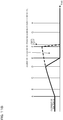
- Fig. 2A to Fig. 2D illustrate timing charts of the operations of the direct-current interruption apparatus illustrated in Fig. 1 .
- the time-series operations of the direct-current interruption apparatus illustrated in Fig. 1 will be described with reference to Fig. 2A to Fig. 2D .
- Fig. 2A illustrates a time-series variation of the total current (that is, the current detected by the current detecting unit 31).
- the initial stage stage before the time A is a normal state where a current is flowing, and this current is the total current flowing in the switches 11, 12.
- the current does not flow to the semiconductor switch 22, nor to the commutation element 21, the reactor 23, or the nonlinear resistor 24.
- the control unit 40 finds that a fault has occurred from the information obtained from the fault detector (not illustrated) or from the detected current notified by the current detecting unit 31 (time B). Upon finding the fault occurrence, the control unit 40 starts the electrode open control over the switches 11, 21 (time C). Even when the electrode open control is started, an arc current continues flowing to the switches 11, 12. In this state, the discharging of the commutation element is started under the control by the control unit 40 (time D).
- the discharging of the commutation element 21 is started, specifically, by changing the semiconductor switch 21b to ON.
- the semiconductor switch 21b changes to ON, the discharge of the electric charge stored in the charge/discharge functional element 21a in advance occurs to decrease the voltage across the both electrodes of the charge/discharge functional element 21a toward zero, so that the current flowing to the switch 12 is quickly commutated to be the current passing the commutation element 21. More specific description will be given below.
- a state where the electrodes on the lower side and the upper side in the drawing of the charge/discharge functional element 21a are charged plus and minus respectively in advance and the semiconductor switch 21b is OFF is equivalent to a state where one of the electrodes of the charge/discharge functional element 21a is electrically open, and in this state, the discharge scarcely occurs.
- the semiconductor switch 21b changes to ON from this state the discharge occurs from the electrode on the lower side in the drawing of the charge/discharge functional element 21a to the electrode on the upper side in the drawing of the charge/discharge functional element 21a through the semiconductor switch 21b, the reactor 23, and the switch 12.
- a voltage starts to be generated across the switch 12 owing to an on-resistance of the semiconductor switch 21b (refer to Fig. 2D ).
- the length from the time D to the time E is adjustable by the inductance of the reactor 23 as roughly described above.
- the time D is preferably at or after the opening time at which the interelectrode distance of the switch 12 is assumed to reach the predetermined distance.
- the semiconductor switch 21b of the commutation element 21 is next changed to OFF under the control by the control unit 40 (time F). That is, the control unit 40 estimates the length from the time D to the time E and performs the OFF control over the semiconductor switch 21b at or after the commutation time (time E) at which the current flowing in the switch 12 is assumed to reach zero.
- the control unit 40 By the OFF control over the semiconductor switch 21b by the control unit 40, the current path leading to the semiconductor switch 21b through the switch 11 is disconnected. Accordingly, the current having been flowing to the switch 11 until then is commutated this time to be a current to the semiconductor switch 22 which has been brought into a state allowing the current passage (time F: refer to Fig. 2C ). In a period from about the time F up to the time G described next, the voltage drop to a certain degree is occurring in the semiconductor switch 22 owing to the on-resistance of the semiconductor switch 22, and this becomes an applied voltage to the direct-current interruption apparatus (refer to Fig. 2D ).
- the control unit 40 controls the semiconductor switch 22 so as to turn off the semiconductor switch 22, at or after the opening time at which the interelectrode distance of the switch 11 is assumed to reach the predetermined distance (time G).
- time G the predetermined distance
- the current path 10 having the switches 11, 12 has already been in the current interruption state which is established at a timing soon after the time F, and the semiconductor switch 22 is also changed to the current interruption state at the time G. Accordingly, at and after the time G, the current temporarily flows to the nonlinear resistor 24.
- a relatively large voltage drop for example, 500 kV
- the current flows to the nonlinear resistor 24 its resistance value increases owing to the nonlinearity of the resistance, and the increased resistance value decreases the current to substantially zero.
- time H for example, several ms from the time A.
- a state from the time H is a state where a direct-current voltage (for example, 300 kV) appropriate for the direct-current power transmission system is applied to the direct-current interruption apparatus (refer to Fig. 2D ).
- the above-described time-series controls by the control unit 40 enable a series of the interruption controls as the direct-current interruption apparatus.
- This control procedure can be said as a basic procedure in this direct-current interruption apparatus, and the controls for the interruption may take place at more precise preferable timings without departing from this basic procedure (to be described later).
- the non-use of a semiconductor switch in the current path 10 makes it possible to greatly reduce a power loss during the current passage.
- the switch 11 is lower in responsiveness to the electrode open control but is higher in withstand voltage characteristics than the switch 12.
- the switch 12 is higher in responsiveness to the electrode open control but is lower in withstand voltage characteristics than the switch 11.
- the series connection of the high-withstand voltage switch 11 with the low-withstand voltage switch 12 achieves a withstand voltage high enough as the direct-current interruption apparatus.
- the commutation element 21 inserted in parallel with the switch 12 works to forcibly commutate the current of the switch 12 quickly to the commutation element 21 according to the switch 12 high in responsiveness.
- the semiconductor switch 21b of the commutation element 21 is thereafter changed to OFF, it is possible to quickly commutate the current of the switch 11 this time toward the semiconductor switch 22 as a current to be interrupted. Accordingly, it is possible to change the semiconductor switch 22 to OFF before the value of the interruption target current commutated to the second semiconductor switch 22 increases very much. This enables to avoid an increase in size of the interruption apparatus.
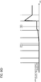
- Fig. 3 is a sectional view schematically illustrating a vacuum valve being an element that may be included in the switch 12 illustrated in Fig. 1 .
- the vacuum valve 50 includes, as its main components, a porcelain tube 51, a fixed-side electrode 52, a movable-side electrode 53, a fixed-side current-carrying shaft 54, a movable-side current-carrying shaft 55, and a bellows 56.
- a vacuum switch is usable as the switch 12.
- the vacuum switch is relatively high in responsiveness though it cannot be generally said to be a switch having a high withstand voltage characteristics. Therefore, even if the vacuum switch is used as the switch 12, the switch 12 can endure a low applied voltage which is possibly generated by the commutation element 21 including the semiconductor switch 21b in an ON state after the current of the current path 10 is reduced to zero, and in addition, there is an advantage that it is possible to reduce the time required for the commutation of the current of the switch 12.
- the vacuum switch includes the vacuum valve 50 illustrated in Fig. 3 , and in addition includes a mechanism (not illustrated) for moving the movable-side current-carrying shaft 55 in its axial direction as desired.
- the inside of the cylindrical porcelain tube 51 is kept substantially vacuum, and in order to insulate this vacuum from the outside, the bellows 56 is fixed to the movable-side current-carrying shaft 55 and the porcelain tube 51.
- the structure of the vacuum valve 50 will be described below.
- the fixed-side current-carrying shaft 54 penetrates through an upper surface of the cylindrical porcelain tube, and the fixed-side current-carrying shaft 54 is fixed to the porcelain tube 51 at a portion where it penetrates to the porcelain tube 51.
- a portion penetrating to and protruding from the upper surface of the cylindrical porcelain tube 51 is one terminal of the switch.
- the flat and disk-shaped fixed-side electrode 52 is at one end of the fixed-side current-carrying shaft 54 located inside the porcelain tube 51, so as to be coaxial with the fixed-side current-carrying shaft 54.
- a face of the movable-side electrode 53 having the same shape as that of the fixed-side electrode 52 and coaxial with the fixed-side electrode 52 faces a face of the fixed-side electrode 52 on a side opposite to a side where the fixed-side current-carrying shaft 54 is located.
- the movable-side current-carrying shaft 55 is located on a side of the movable-side electrode 53 opposite to its face facing the fixed-side current-carrying shaft 52, so as to be coaxial with the fixed-side current-carrying shaft 54, the fixed-side electrode 52, and the movable-side electrode 53.
- the movable-side current-carrying shaft 55 penetrates through a lower surface of the cylindrical porcelain tube 51, and its portion penetrating and protruding is the other terminal of the switch.
- the bellows 56 has its one side fixed to the movable-side current-carrying shaft 55 and has the other end fixed to the porcelain tube 51. The bellows 56 constantly keeps the inside of the porcelain tube 51 airtight even if the movable-side current-carrying shaft 55 is moved in its axial direction in order to pass or interrupt the current.
- the direct-current interruption apparatus illustrated in Fig. 1 is used in a system of, for example, about 300 kV direct current, it may almost suffice if the switch 12 can endure the voltage drop by the commutation element 21 including the semiconductor switch 21b in the ON state, considering the structure of this apparatus in which the high-withstand voltage switch 11 is connected in series with the switch 12. This voltage drop is estimated as several kV at the largest, and even the switch 12 being the vacuum switch can easily endure the voltage on this level. In addition, the use of the switch 12 being the vacuum switch enables a reduction in the time required for the commutation from the switch 12.
- one having plate electrodes as the electrodes 52, 53 is especially advantageous in terms of a reduction in a power loss during the current passage because of its low electric resistance in the closed state.
- a vacuum switch including vertical magnetic field electrodes as the electrodes 52, 53 can have improved interruption performance and its electrodes are less damaged because an arc current flowing between its electrodes after the electrode open control is controlled to diffuse by a vertical magnetic field.
- Examples of the vertical magnetic field electrodes are a fixed-side electrode 52a and a current-carrying side electrode 53a having slits on their side faces so that a circumferential-direction component is added to the direction of the current as schematically illustrated in Fig. 4 .
- the vertical magnetic field is added to the arc current between the electrodes 52a, 53a, and consequently, charged particles are confined in the magnetic field to equally distribute to the whole electrodes 52a, 53a. This can improve interruption performance and reduce damage to the electrodes.
- a specific example of the switch 11 is not mentioned either in the description of Fig. 1 and Fig. 2A to Fig. 2D , but a gas switch filled with SF 6 as insulating gas is usable as the switch 11, for instance.
- the gas switch is typically high in withstand voltage characteristics. Therefore, the use of the gas switch as the switch 11 enables the switch 11 to receive and endure a high applied voltage to the direct-current interruption apparatus that is possibly generated after the current interruption. At this time, the high applied voltage to the direct-current interruption apparatus is borne mainly by the switch 11 since the commutation element 21 (its resistance is not infinitely large, though high) in the OFF state is in parallel with the other switch 12.
- FIG. 5 illustrates the configuration of the direct-current interruption apparatus of the second embodiment (No. 1).
- the same components as those illustrated in Fig. 1 will be denoted by the same reference signs and description thereof will be omitted.
- this second embodiment is different from that illustrated in Fig. 1 in that the nonlinear resistor 24 in the second embodiment is connected in parallel with a series element of the semiconductor switch 22 and the reactor 23.
- the nonlinear resistor 24 may be connected in parallel only with the semiconductor switch 22 as illustrated in Fig. 1 , and may alternatively be connected in parallel with the series element of the semiconductor switch 22 and the reactor 23 as described here.
- the purpose of the reactor 23 is to adjust the time from the start of the discharging of the commutation element 21 until the current of the switch 12 is reduced to zero.
- the nonlinear resistor 24 the current only temporarily flows at the final stage of the direct-current interruption. Therefore, in whichever manner the nonlinear resistor 24 is arranged, there is substantially no influence on the function of the temporary current flow, that is, the direct-current interruption operation.
- Fig. 6 illustrates the configuration of the direct-current interruption apparatus of the second embodiment (No. 2).
- the same components as those illustrated in Fig. 1 will be denoted by the same reference signs and description thereof will be omitted.
- the configuration of this second embodiment is different from that illustrated in Fig. 1 in that the reactor 23 of the second embodiment is inserted in series only with the commutation element 21. That is, the reactor 23 is not in a series positional relation with the semiconductor switch 22, nor with the nonlinear resistor 24. It can also be said that the commutation element 21 is replaced by a series connection element of the charge/discharge functional element 21a, the semiconductor switch 21b, and the rector 23. The reactor 23 may also be in such an arrangement.
- the purpose of the reactor 23 is to adjust the time from the start of the discharging of the commutation element 21 until the current of the switch 12 is reduced to zero, which easily leads to the conclusion that the reactor 23 may be in the arrangement illustrated in Fig. 6 .
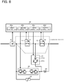
- FIG. 7 illustrates the configuration of the direct-current interruption apparatus of the third embodiment.
- the same components as those illustrated in Fig. 1 will be denoted by the same reference signs and description thereof will be omitted.
- a current path 10A of the third embodiment further includes an additional element 13 which is connected in parallel with the switch 12 and functions to reduce the maximum voltage that is possibly applied to the switch 12. Disposing the additional element 13 in parallel with the switch 12 makes it possible to further obviously reduce the maximum voltage applied to the switch 12, owing to its configuration difference from the switch 11 not provided with such an additional element.
- the additional element 13 one of a resistor, a nonlinear resistor, a capacitor, and a series connection element of a capacitor and a resistor, or one in which two or more these are connected in parallel is adoptable, for instance.
- the additional element 13 is a resistor or a nonlinear resistor (for example, a zinc oxide element)
- a resistance-divided voltage is applied to the switch 12, owing to its configuration difference from the switch 11 (small resistance, small applied voltage).
- the additional element 13 is a capacitor
- a capacitance-divided voltage is applied to the switch 12, owing to its configuration difference from the switch 11 (large capacitance, small applied voltage).
- an impedance-divided voltage is applied to the switch 12, owing to its configuration difference from the switch 11 (small impedance, small applied voltage).
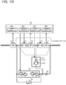
- FIG. 8 illustrates the configuration of the direct-current interruption apparatus of the fourth embodiment.
- the same components as those illustrated in Fig. 1 will be denoted by the same reference signs and description thereof will be omitted.
- a current path 10B of the fourth embodiment includes a distance detecting unit 14 provided on the switch 11 to detect the interelectrode distance of the switch 11 and notify it to the control unit 40, and also includes a distance detecting unit 15 provided on the switch 12 to detect the interelectrode distance of the switch 12 and notify it to the control unit 40.
- the distance detecting unit 14 provided on the switch 11 notifies the detected interelectrode distance of the switch 11 to the fourth control unit 40d.
- the fourth control unit 40d performs the control for changing the semiconductor switch 22 to OFF at an instant that is after the third control unit 40c performs the OFF control for changing the semiconductor switch 21b to OFF and that is at or after the opening time at which the distance detecting unit 14 detects that the interelectrode distance of the switch 11 reaches a predetermined distance.
- the distance detecting unit 15 provided on the second switch 12 notifies the detected interelectrode distance of the switch 12 to the third control unit 40c.
- the third control unit 40c performs the discharge control at an instant that is after the first control unit 40a starts the electrode open control over the switch 11 and the second control unit 40b starts the electrode open control over the switch 12 and that is at or after the opening time at which the distance detecting unit 15 detects that the interelectrode distance of the switch 12 reaches a predetermined distance.
- the control unit 40 performs the discharge control over the commutation element 21, the gradual reduction of the current flowing to the switch 12 starts and the application of the voltage to the switch 12 starts, as previously described. Therefore, according to this embodiment, since the control unit 40 is capable of performing the discharge control over the commutation element 21 based on the detected result of the interelectrode distance of the switch 12, the voltage is applied to the switch 12 having the interelectrode distance large enough for preventing a problem that might be caused by the generated voltage, and this is preferable.
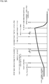
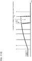
- Fig. 9A to Fig. 9D illustrate timing charts of the operations of the direct-current interruption apparatus illustrated in Fig. 8 .
- Fig. 9A to Fig. 9D are substantially the same as Fig. 2A to Fig. 2D , and for the same points, refer to the contents already described. The points described with reference to Fig. 8 will be described again with reference to Fig. 9 .
- the discharging of the commutation element 21 is started, and this is a preferable timing.
- the semiconductor switch 22 is changed to OFF, and this is a preferable timing.
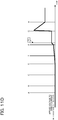
- Fig. 10 illustrates the configuration of the direct-current interruption apparatus of the fifth embodiment.
- the same components as those illustrated in Fig. 1 will be denoted by the same reference signs and description thereof will be omitted.
- a current path 10C of the fifth embodiment includes a current detecting unit 16 connected in series with the switch 11 and detects the current flowing in the switch 11 to notify it to the control unit 40, and also includes a current detecting unit 17 connected in series with the switch 12 and detects the current flowing in the switch 12 to notify it to the control unit 40.
- a current detecting unit 16 connected in series with the switch 11 and detects the current flowing in the switch 11 to notify it to the control unit 40
- a current detecting unit 17 connected in series with the switch 12 and detects the current flowing in the switch 12 to notify it to the control unit 40.
- the current detecting unit 16 connected in series with the switch 11 and detects the current flowing in the switch 11 notifies the detected current to the fourth control unit 40d.
- the fourth control unit 40d performs the control for changing the semiconductor switch 22 to OFF at an instant that is after the third control unit 40c performs the OFF control for changing the semiconductor switch 21a to OFF and that is at or after the commutation time at which the current detecting unit 16 detects that the current flowing in the switch 11 reaches zero.
- the current detecting unit 17 connected in series with the switch 12 and detects the current flowing in the switch 12 notifies the detected current to the third control unit 40c.
- the third control unit 40c performs the OFF control at an instant that is after the third control unit 40c performs the control for discharging the charge/discharge functional element 21a and that is at or after the commutation time at which the current detecting unit 17 detects that the current flowing in the switch 12 reaches zero.
- the series connection of the current detecting unit 17 with the switch 12 has the following advantage.
- the control for discharging the functional element 21a of the commutation element 21 by the control unit 40 is performed so as to reduce the current flowing in the switch 12 to zero. Consequently, the commutation of the current flowing to the switch 12 is completed. It takes some time for the current flowing in the switch 12 to actually reach zero after the discharge control. Therefore, it is preferable to perform the OFF control over the semiconductor switch 21b, which is the next control, taking this time into account.
- from the current detecting unit 17 it is possible to find that the current has reached zero, enabling a more appropriate response to this state.
- the series connection of the current detecting unit 16 with the switch 11 has the following advantage. This configuration makes it possible to assume an instant at which the current detecting unit 11 detects that the current flowing in the switch 11 reaches zero, as an instant at which the interelectrode distance of the switch 11 has reached the predetermined distance. A reason for this is as follows.
- Fig. 11A to Fig. 11D illustrate timing charts of the operations of the direct-current interruption apparatus illustrated in Fig. 10 .
- Fig. 11A to Fig. 11D are almost the same as Fig. 2A to Fig. 2D , and for the same points, refer to the contents already described.
- the points described with reference to Fig. 10 will be described again with reference to Figs. 11 .
- the commutation element 21 is controlled to be OFF. This is a preferable timing.
- the semiconductor switch 22 is changed to OFF. This is a preferable timing.
- the non-use of a semiconductor switch in the current path enables a great reduction in a power loss during the current passage.
- the first switch 11 is higher in withstand voltage characteristics than the second switch 12, though lower in responsiveness to the electrode open control than the second switch 12.
- the second switch 12 is lower in withstand voltage characteristics than the first switch, though higher in responsiveness to the electrode open control than the first switch 11.
- the series connection of the high-withstand voltage switch 11 with the low-withstand voltage switch 12 achieves a withstand voltage characteristics high enough as the direct-current interruption apparatus.
- the work of the commutation element 21 makes it possible to forcibly commutate the current quickly to the commutation element 21 according to the switch 12 with high responsiveness.
- the first semiconductor switch 21b of the commutation element 21 is thereafter changed to OFF, it is possible this time to commutate the current of the first switch 11 quickly to the second semiconductor switch 22 as the current to be interrupted. Accordingly, it is possible to change the second semiconductor switch 22 to OFF before the value of the interruption target current commutated to the second semiconductor switch 22 increases very much. This enables to avoid an increase in size of the interruption apparatus.
Abstract
Description
- Embodiments of the present invention relate to a direct-current interruption apparatus and a direct-current interruption method for interrupting a direct current.
- A system for transmitting electric power is typically required to have a function of interrupting a power transmission current in case of, for example, a fault. An interruption apparatus is used for this purpose, but direct-current power transmission, in particular, has a difficulty that alternating-current interruption does not have because a direct current transmitted in the direct-current power transmission does not have a zero point.
- A currently used direct-current interruption apparatus includes, for example, a current path having a switch and a current-interrupting path which is in parallel with the current path and is capable of gradually decreasing a current. The switch on the current path is normally closed to allow the passage of the current through the current path.
When a fault occurs, the current-interrupting path temporarily becomes electrically open so as to allow a fault current to pass through the current-interrupting path instead of the current path. On the other hand, the switch is opened to interrupt the current flowing to the current path, thereby commutating the fault current toward the current-interrupting path. The current of the current-interrupting path is thereafter quickly limited. This is the completion of the interruption. - The current path of the direct-current interruption apparatus preferably has as small an electric resistance as possible. This is because the electric resistance is a power loss during the normal time. In the direct-current interruption apparatus, the switching of the direction of the current from the current path to the current-interrupting path is preferably as prompt as possible. This is because, as the switching is more delayed, the fault current increases more, leading to an increase in a value of the current that is to be interrupted by the current-interrupting path. The increase in the current to be interrupted necessitates a larger capacity of the current-interrupting path, leading to a size increase of the interruption apparatus.
-
- Non-patent Document 1: Juergen Haefner, Bjoern Jacobson, "Proactive Hybrid HVDC Breakers - A key innovation for reliable HVDC grids", The electric power system of the future - Integrating supergrids and microgrids, International Symposium in Bologna, Italy 13-15 September, 2011
- Non-patent Document 2: Per Skarby, Ueli Steiger, "An Ultra-fast Disconnecting Switch for a Hybrid HVDC Breaker - a technical breakthrough", Ciger, Canada conference, Calgary, Canada 9-11 September, 2013
- A problem to be solved by the invention is to provide a direct-current interruption apparatus and a direct-current interruption method which enable to reduce a power loss during the normal time and avoid an increase in apparatus size.
- A direct-current interruption apparatus of an embodiment includes a current path, a commutation element including a first semiconductor switch, a second semiconductor switch, a conductive path, and a nonlinear resistor. The current path includes a first switch and a second switch connected in series, the first switch being a non-semiconductor device and having a predetermined first withstand voltage, and the second switch being a non-semiconductor device and having a second withstand voltage lower than the first withstand voltage.
- The commutation element has one end connected with a connection node of the first switch and the second switch and includes a functional element and the first semiconductor switch connected in series, the functional element having a charge/discharge function. The second semiconductor switch is between and connects with the other end of the commutation element and one end of the first switch, opposite to one end of the first switch connected with the second switch. The conductive path is between and connects with the other end of the commutation element and one end of the second switch, opposite to one end of the second switch connected with the first switch. The nonlinear resistor is connected in parallel with the second semiconductor switch.
- A direct-current interruption method of an embodiment is a direct-current interruption method of the above-described direct-current interruption apparatus and is as follows. Specifically, the method includes (1) charging the functional element of the commutation element in advance, (2) discharging the functional element after starting electrode open control over the first switch and starting electrode open control over the second switch, (3) changing the first semiconductor switch to OFF after discharging the functional element, and (4) changing the second semiconductor switch to OFF after changing the first semiconductor switch to OFF.
-
-
Fig. 1 is a block diagram illustrating a direct-current interruption apparatus of a first embodiment. -
Fig. 2A is an explanatory timing chart of the operation of the direct-current interruption apparatus illustrated inFig. 1 (total current). -
Fig. 2B is an explanatory timing chart of the operation of the direct-current interruption apparatus illustrated inFig. 1 (current of a switch 12). -
Fig. 2C is an explanatory timing chart of the operation of the direct-current interruption apparatus illustrated inFig. 1 (current of a switch 11). -
Fig. 2D is an explanatory timing chart of the operation of the direct-current interruption apparatus illustrated inFig. 1 (applied voltage to the direct-current interruption apparatus). -
Fig. 3 is a sectional view schematically illustrating a vacuum valve being an element that may be included in theswitch 12 illustrated inFig. 1 . -
Fig. 4 is a perspective view schematically illustrating a modification example of electrodes of the vacuum valve illustrated inFig. 3 . -
Fig. 5 is a block diagram illustrating a direct-current interruption apparatus of a second embodiment (No. 1). -
Fig. 6 is a block diagram illustrating a direct-current interruption apparatus of the second embodiment (No. 2). -
Fig. 7 is a block diagram illustrating a direct-current interruption apparatus of a third embodiment. -
Fig. 8 is a block diagram illustrating a direct-current interruption apparatus of a fourth embodiment. -
Fig. 9A is an explanatory timing chart of the operation of the direct-current interruption apparatus illustrated inFig. 8 (total current). -
Fig. 9B is an explanatory timing chart of the operation of the direct-current interruption apparatus illustrated inFig. 8 (current of a switch 12). -
Fig. 9C is an explanatory timing chart of the operation of the direct-current interruption apparatus illustrated inFig. 8 (current of a switch 11). -
Fig. 9D is an explanatory timing chart of the operation of the direct-current interruption apparatus illustrated inFig. 8 (applied voltage to the direct-current interruption apparatus). -
Fig. 10 is a block diagram illustrating a direct-current interruption apparatus of a fifth embodiment. -
Fig. 11A is an explanatory timing chart of the operation of the direct-current interruption apparatus illustrated inFig. 10 (total current). -
Fig. 11B is an explanatory timing chart of the operation of the direct-current interruption apparatus illustrated inFig. 10 (current of a switch 12). -
Fig. 11C is an explanatory timing chart of the operation of the direct-current interruption apparatus illustrated inFig. 10 (current of a switch 11). -
Fig. 11D is an explanatory timing chart of the operation of the direct-current interruption apparatus illustrated inFig. 10 (applied voltage to the direct-current interruption apparatus). - Based on the above, a direct-current interruption apparatus of each embodiment will be hereinafter described with reference to the drawings.
Fig. 1 illustrates the configuration of the direct-current interruption apparatus of a first embodiment. As illustrated inFig. 1 , the direct-current interruption apparatus includes acurrent path 10, acommutation element 21, asemiconductor switch 22, areactor 23, anonlinear resistor 24, a current detectingunit 31, and acontrol unit 40. Thecommutation element 21 includes a charge/dischargefunctional element 21a and asemiconductor switch 21b connected in series. - The
current path 10 includes aswitch 11 and aswitch 12 connected in series, theswitch 11 having a predetermined large withstand voltage characteristics (to be described later) and theswitch 12 having a lower withstand voltage characteristics than that of theswitch 11. Theswitches switch 11 and theswitch 12, theswitch 12 is higher in responsiveness to electrode open control. However, being a non-semiconductor device, even theswitch 12 is not capable of responding as quickly as a semiconductor device. In the following description, theswitch 11 and theswitch 12 will be sometimes comprehensively referred to as a switch group. - The operation of this apparatus is roughly as follows. The
switches current path 10. When the interruption of the current is required because of, for example, a fault, the electrode open control over theswitches switch 12 reaching the electrode open state first, thecommutation element 21 is made to function to promptly commutate the current flowing to theswitch 12 to a path passing thecommutation element 21. - Immediately after the commutation, the electrode open control over the
switch 11 has not been completed and the current flows to theswitch 11. Thereafter, when thesemiconductor switch 21b of thecommutation element 21 is promptly changed to OFF, the current which continues flowing to theswitch 11 is commutated to a path passing thesemiconductor switch 22 which has been controlled so as to allow the passage of the current. Thereafter, when thesemiconductor switch 22 is changed to OFF, the current is limited. This is the completion of the interruption. - In
Fig. 1 , both cases are generally conceivable where the flow direction of a direct current during the normal time is left to right in the drawing and it is right to left in the drawing, and the direct-current interruption apparatus is adapted to the both cases. For the convenience of the description, it is hereinafter assumed that the flow direction of the direct current is normally from left to right in the drawing. First, the components illustrated inFig. 1 will be described. - The
switch 11 is, as described above, a non-semiconductor device (mechanical device) and is capable of switching between the passage and interruption of a current. Theswitch 12 is also a non-semiconductor device and is capable of switching between the passage and interruption of a current. Theswitch 11 and theswitch 12 are in a complementary relation in terms of their advantages of withstand voltage characteristics and response speed to the electrode open control, and the switches thus having different characteristics are connected in series so that they each take its share of functions. The opening and closing of electrodes of both theswitch 11 and theswitch 12 are controlled by thecontrol unit 40. - The
commutation element 21 has one end connected with a connection node of theswitch 11 and theswitch 12 to commutate the current flowing to theswitch 12 quickly to the path passing the commutation element 21 (and the reactor 23). Thecommutation element 21 includes a charge/dischargefunctional element 21 a (for example, a capacitor) and asemiconductor switch 21b connected in series. - The charge/discharge
functional element 21a is charged in advance under the control by thecontrol unit 40, and when thesemiconductor switch 21b changes to ON in this state, a discharge of stored charge occurs to decrease a voltage across electrodes of the charge/dischargefunctional element 21a toward zero, so that the current flowing to theswitch 12 is quickly commutated to be a current passing thecommutation element 21. The charging and discharging of thecommutation element 21 are controlled by thecontrol unit 40. - The
semiconductor switch 22 is between and connects with the other end of thecommutation element 21 and one end of theswitch 11, opposite to one end of theswitch 11 connected with theswitch 12. Thesemiconductor switch 22 switches between the passage and interruption of a current and its switching (ON/OFF) is controlled by thecontrol unit 40. - A specific example of the
semiconductor switch 22 is a structure including many series-connected unit elements and having two main electrode terminals as a whole, the unit elements each being an element in which two inverse parallel connection (parallel connection with opposite forward directions) elements each composed of an IGBT (insulated gate bipolar transistor) and a diode are in face-to-face series connection in opposite directions, as illustrated inFig. 1 . When a voltage ascribable to a control signal from thecontrol unit 40 is applied to gates of IGBTs, the unit elements get into a state where the current flows in any direction (that is, the ON state). - As a specific structure of the
semiconductor switch 22, various structures are adoptable besides the illustrated one. For example, adoptable is a structure composed of may series-connected unit elements and having two main electrode terminals as a whole, the unit elements each being composed of thyristors which are in inverse parallel connection. A semiconductor switch typically has an equivalent resistance in an ON state (on-resistance), and undergoes a voltage drop when supplied with a current. This voltage drop is larger depending on the number of the series-connected unit elements, that is, the on-resistance of thewhole semiconductor switch 22 also is larger depending on this series-connection number. - The necessary number of the series-connected unit elements can be decided so as to satisfy the condition that it can endure a high voltage that is possibly applied to the interruption apparatus at and after an instant when the
semiconductor switch 22 becomes OFF for the current interruption. To achieve this, the series-connection number usually needs to be large to a certain degree (for example, several hundreds). - A standard way of the switching control over the
semiconductor switch 22 by thecontrol unit 40 is to keep thesemiconductor switch 22 OFF during the normal time, temporarily change thesemiconductor switch 22 to ON at the time of the interruption operation, and thereafter quickly change thesemiconductor switch 22 to OFF. However, this is not restrictive. Even if thesemiconductor switch 22 is controlled to be kept ON during the normal time, its on-resistance prevents a current from actually flowing thereto, and the total current flows in the current carryingpath 10. Therefore, the control to thus keep thesemiconductor switch 22 ON during the normal time is also an adoptable selection. - The
reactor 23 is between and connected with the other end of thecommutation element 21 and one end of theswitch 12, opposite to one end of theswitch 12 connected with theswitch 11. The purpose of the insertedreactor 23 is to adjust the time from the start of the discharging of thecommutation element 21 up to an instant at which the current of theswitch 12 is reduced to zero. The timing at which the current is reduced to zero is preferably after the completion and establishment of the electrode open control over theswitch 12, and by disposing thereactor 23 in the illustrated manner and adjusting its reactance, it is possible to reduce a discharge current to enable the aforesaid adjustment. In a case where the necessity for the adjustment is low, a simple conducting wire may replace thereactor 23. - The
nonlinear resistor 24 is connected in parallel with thesemiconductor switch 22. Thenonlinear resistor 24 functions at a final stage of the interruption operation of the direct-current interruption apparatus. Specifically, when the current to thecurrent path 10 is interrupted and the current to thesemiconductor switch 22 is also interrupted, the current temporarily flows to thenonlinear resistor 24. At an initial stage of the temporary flow, a current having the same value as that of the current flowing to thesemiconductor switch 22 immediately before this stage flows. When the current flows, a resistance value increases due to the nonlinearity of resistance, and the increased resistance value causes the current to be substantially zero. This is the completion of the current interruption. - The current detecting
unit 31 detects a current flowing in the direct-current interruption apparatus and notifies thecontrol unit 40 of the detected current. For this purpose, the current detectingunit 31 is outside the parallel connection of theswitches semiconductor switch 22, and thenonlinear resistor 24 so as to be connected in series with this parallel connection. Specific examples of how the current is detected include a structure to insert a resistor having a very small resistance value and detect a voltage across the resistor, and a structure to detect a magnetic flux generated by the current (direct-current CT). - The
control unit 40 controls the opening and closing of the electrodes of theswitches commutation element 21, and ON/OFF of thesemiconductor switch 22. Thecontrol unit 40 includes, as lower-order control units corresponding to these controls, afirst control unit 40a, asecond control unit 40b, athird control unit 40c, and afourth control unit 40d, and among these lower-order control units, information necessary for their controls is transmitted so as to be shared among them. - The
first control unit 40a connects with theswitch 11 to control the opening and closing of the electrodes of theswitch 11. Thesecond control unit 40b connects with theswitch 12 to control the opening and closing of the electrodes of theswitch 12. Thethird control unit 40c connects with thecommutation element 21 and the first andsecond control units third control unit 40c controls ON/OFF of thesemiconductor switch 21b of thecommutation element 21 and also has a control function of charging the charge/dischargefunctional element 21a of thecommutation element 21 in advance and discharging it at a predetermined timing. - The
third control unit 40c has at least the following functions. Specifically, thethird control unit 40c performs the charge control for charging the charge/dischargefunctional element 21a in advance before the start of the electrode open control over theswitch 11 by thefirst control unit 40a and the start of the electrode open control over theswitch 12 by thesecond control unit 40b, performs the discharge control for discharging the charge/dischargefunctional element 21a after the start of the electrode open control over theswitch 11 by thefirst control unit 40a and the start of the electrode open control over theswitch 12 by thesecond control unit 40b, and performs the OFF control for changing thesemiconductor switch 21b to OFF after performing the discharge control. - The discharge control that the
third control unit 40c performs after the start of the electrode open control over theswitch 11 by thefirst control unit 40a and the electrode open control over theswitch 12 by thesecond control unit 40b takes place at or after the opening time at which the interelectrode distance of theswitch 12 is assumed to reach a predetermined distance. - The OFF control that the
third control unit 40c performs after performing the control for discharging the charge/dischargefunctional element 21a takes place at or after the commutation time at which the current flowing in theswitch 12 is assumed to reach substantially zero. - The
fourth control unit 40d connects with thesemiconductor switch 22 and thethird control unit 40c and controls ON/OFF of thesemiconductor switch 22. Thefourth control unit 40d at least has a function of performing the control for changing thesemiconductor switch 22 to OFF after thethird control unit 40c performs the OFF control. - The control for changing the
semiconductor switch 22 to OFF performed by thefourth control unit 40d after thethird control unit 40c performs the OFF control takes place at or after the opening time at which the interelectrode distance of theswitch 11 is assumed to reach a predetermined distance. - The
control unit 40 obtains information regarding a fault from a fault detector (not illustrated), but thecontrol unit 40 may determine that a fault has occurred by making use of the detected current notified from the current detectingunit 31. -
Fig. 2A to Fig. 2D illustrate timing charts of the operations of the direct-current interruption apparatus illustrated inFig. 1 . The time-series operations of the direct-current interruption apparatus illustrated inFig. 1 will be described with reference toFig. 2A to Fig. 2D . -
Fig. 2A illustrates a time-series variation of the total current (that is, the current detected by the current detecting unit 31). InFig. 2A , the initial stage (stage before the time A is a normal state where a current is flowing, and this current is the total current flowing in theswitches semiconductor switch 22, nor to thecommutation element 21, thereactor 23, or thenonlinear resistor 24. - When a fault occurs in a direct-current power transmission system at the time A, the total current gradually increases as illustrated in
Fig. 2A . Thecontrol unit 40 finds that a fault has occurred from the information obtained from the fault detector (not illustrated) or from the detected current notified by the current detecting unit 31 (time B). Upon finding the fault occurrence, thecontrol unit 40 starts the electrode open control over theswitches 11, 21 (time C). Even when the electrode open control is started, an arc current continues flowing to theswitches - The discharging of the
commutation element 21 is started, specifically, by changing thesemiconductor switch 21b to ON. When thesemiconductor switch 21b changes to ON, the discharge of the electric charge stored in the charge/dischargefunctional element 21a in advance occurs to decrease the voltage across the both electrodes of the charge/dischargefunctional element 21a toward zero, so that the current flowing to theswitch 12 is quickly commutated to be the current passing thecommutation element 21. More specific description will be given below. - A state where the electrodes on the lower side and the upper side in the drawing of the charge/discharge
functional element 21a are charged plus and minus respectively in advance and thesemiconductor switch 21b is OFF is equivalent to a state where one of the electrodes of the charge/dischargefunctional element 21a is electrically open, and in this state, the discharge scarcely occurs. When thesemiconductor switch 21b changes to ON from this state, the discharge occurs from the electrode on the lower side in the drawing of the charge/dischargefunctional element 21a to the electrode on the upper side in the drawing of the charge/dischargefunctional element 21a through thesemiconductor switch 21b, thereactor 23, and theswitch 12. - In the
switch 12, the direction of this discharge current is opposite to that of the current having been flowing until then, and accordingly, the current having been flowing to theswitch 12 is quickly commutated to be the current passing thecommutation element 21. Consequently, the current interruption of theswitch 12 is completed (time E: refer toFig. 2B ). - At or after the time D at which the discharging of the
commutation element 21 is started, a voltage starts to be generated across theswitch 12 owing to an on-resistance of thesemiconductor switch 21b (refer toFig. 2D ). The length from the time D to the time E is adjustable by the inductance of thereactor 23 as roughly described above. However, since at or after the time D, the voltage can be generated across theswitch 12, the time D is preferably at or after the opening time at which the interelectrode distance of theswitch 12 is assumed to reach the predetermined distance. - Even after the aforesaid time E, the current continues flowing to the
switch 11 because of its low responsiveness to the electrode open control (refer toFig. 2C ). In this state, thesemiconductor switch 21b of thecommutation element 21 is next changed to OFF under the control by the control unit 40 (time F). That is, thecontrol unit 40 estimates the length from the time D to the time E and performs the OFF control over thesemiconductor switch 21b at or after the commutation time (time E) at which the current flowing in theswitch 12 is assumed to reach zero. - By the OFF control over the
semiconductor switch 21b by thecontrol unit 40, the current path leading to thesemiconductor switch 21b through theswitch 11 is disconnected. Accordingly, the current having been flowing to theswitch 11 until then is commutated this time to be a current to thesemiconductor switch 22 which has been brought into a state allowing the current passage (time F: refer toFig. 2C ). In a period from about the time F up to the time G described next, the voltage drop to a certain degree is occurring in thesemiconductor switch 22 owing to the on-resistance of thesemiconductor switch 22, and this becomes an applied voltage to the direct-current interruption apparatus (refer toFig. 2D ). - After the time F, the
control unit 40 controls thesemiconductor switch 22 so as to turn off thesemiconductor switch 22, at or after the opening time at which the interelectrode distance of theswitch 11 is assumed to reach the predetermined distance (time G). At this time, thecurrent path 10 having theswitches semiconductor switch 22 is also changed to the current interruption state at the time G. Accordingly, at and after the time G, the current temporarily flows to thenonlinear resistor 24. - At the initial stage of the temporary flow, the current having the same value as that of the current flowing to the
semiconductor switch 22 immediately before this stage flows. Consequently, a relatively large voltage drop (for example, 500 kV) occurs in thenonlinear resistor 24. When the current flows to thenonlinear resistor 24, its resistance value increases owing to the nonlinearity of the resistance, and the increased resistance value decreases the current to substantially zero. This is the completion of the current interruption (time H: for example, several ms from the time A). A state from the time H is a state where a direct-current voltage (for example, 300 kV) appropriate for the direct-current power transmission system is applied to the direct-current interruption apparatus (refer toFig. 2D ). - The above-described time-series controls by the
control unit 40 enable a series of the interruption controls as the direct-current interruption apparatus. This control procedure can be said as a basic procedure in this direct-current interruption apparatus, and the controls for the interruption may take place at more precise preferable timings without departing from this basic procedure (to be described later). - As described hitherto, according to the direct-current interruption apparatus of this embodiment, the non-use of a semiconductor switch in the
current path 10 makes it possible to greatly reduce a power loss during the current passage. Theswitch 11 is lower in responsiveness to the electrode open control but is higher in withstand voltage characteristics than theswitch 12. Conversely, theswitch 12 is higher in responsiveness to the electrode open control but is lower in withstand voltage characteristics than theswitch 11. The series connection of the high-withstandvoltage switch 11 with the low-withstandvoltage switch 12 achieves a withstand voltage high enough as the direct-current interruption apparatus. - The
commutation element 21 inserted in parallel with theswitch 12 works to forcibly commutate the current of theswitch 12 quickly to thecommutation element 21 according to theswitch 12 high in responsiveness. When thesemiconductor switch 21b of thecommutation element 21 is thereafter changed to OFF, it is possible to quickly commutate the current of theswitch 11 this time toward thesemiconductor switch 22 as a current to be interrupted. Accordingly, it is possible to change thesemiconductor switch 22 to OFF before the value of the interruption target current commutated to thesecond semiconductor switch 22 increases very much. This enables to avoid an increase in size of the interruption apparatus. -
Fig. 3 is a sectional view schematically illustrating a vacuum valve being an element that may be included in theswitch 12 illustrated inFig. 1 . As illustrated inFig. 3 , thevacuum valve 50 includes, as its main components, aporcelain tube 51, a fixed-side electrode 52, a movable-side electrode 53, a fixed-side current-carryingshaft 54, a movable-side current-carryingshaft 55, and a bellows 56. - Though specific examples of the
switch 12 are not mentioned in the description ofFig. 1 andFig. 2A toFig. 2D , a vacuum switch is usable as theswitch 12. The vacuum switch is relatively high in responsiveness though it cannot be generally said to be a switch having a high withstand voltage characteristics. Therefore, even if the vacuum switch is used as theswitch 12, theswitch 12 can endure a low applied voltage which is possibly generated by thecommutation element 21 including thesemiconductor switch 21b in an ON state after the current of thecurrent path 10 is reduced to zero, and in addition, there is an advantage that it is possible to reduce the time required for the commutation of the current of theswitch 12. - The vacuum switch includes the
vacuum valve 50 illustrated inFig. 3 , and in addition includes a mechanism (not illustrated) for moving the movable-side current-carryingshaft 55 in its axial direction as desired. The inside of thecylindrical porcelain tube 51 is kept substantially vacuum, and in order to insulate this vacuum from the outside, thebellows 56 is fixed to the movable-side current-carryingshaft 55 and theporcelain tube 51. The structure of thevacuum valve 50 will be described below. - The fixed-side current-carrying
shaft 54 penetrates through an upper surface of the cylindrical porcelain tube, and the fixed-side current-carryingshaft 54 is fixed to theporcelain tube 51 at a portion where it penetrates to theporcelain tube 51. In the fixed-side current-carryingshaft 54, a portion penetrating to and protruding from the upper surface of thecylindrical porcelain tube 51 is one terminal of the switch. The flat and disk-shaped fixed-side electrode 52 is at one end of the fixed-side current-carryingshaft 54 located inside theporcelain tube 51, so as to be coaxial with the fixed-side current-carryingshaft 54. A face of the movable-side electrode 53 having the same shape as that of the fixed-side electrode 52 and coaxial with the fixed-side electrode 52 faces a face of the fixed-side electrode 52 on a side opposite to a side where the fixed-side current-carryingshaft 54 is located. - The movable-side current-carrying
shaft 55 is located on a side of the movable-side electrode 53 opposite to its face facing the fixed-side current-carryingshaft 52, so as to be coaxial with the fixed-side current-carryingshaft 54, the fixed-side electrode 52, and the movable-side electrode 53. The movable-side current-carryingshaft 55 penetrates through a lower surface of thecylindrical porcelain tube 51, and its portion penetrating and protruding is the other terminal of the switch. As already described, thebellows 56 has its one side fixed to the movable-side current-carryingshaft 55 and has the other end fixed to theporcelain tube 51. The bellows 56 constantly keeps the inside of theporcelain tube 51 airtight even if the movable-side current-carryingshaft 55 is moved in its axial direction in order to pass or interrupt the current. - Assuming that the direct-current interruption apparatus illustrated in
Fig. 1 is used in a system of, for example, about 300 kV direct current, it may almost suffice if theswitch 12 can endure the voltage drop by thecommutation element 21 including thesemiconductor switch 21b in the ON state, considering the structure of this apparatus in which the high-withstandvoltage switch 11 is connected in series with theswitch 12. This voltage drop is estimated as several kV at the largest, and even theswitch 12 being the vacuum switch can easily endure the voltage on this level. In addition, the use of theswitch 12 being the vacuum switch enables a reduction in the time required for the commutation from theswitch 12. - Among vacuum switches, one having plate electrodes as the
electrodes electrodes - Examples of the vertical magnetic field electrodes are a fixed-
side electrode 52a and a current-carryingside electrode 53a having slits on their side faces so that a circumferential-direction component is added to the direction of the current as schematically illustrated inFig. 4 . When the current between theelectrodes electrodes whole electrodes - A specific example of the
switch 11 is not mentioned either in the description ofFig. 1 andFig. 2A toFig. 2D , but a gas switch filled with SF6 as insulating gas is usable as theswitch 11, for instance. The gas switch is typically high in withstand voltage characteristics. Therefore, the use of the gas switch as theswitch 11 enables theswitch 11 to receive and endure a high applied voltage to the direct-current interruption apparatus that is possibly generated after the current interruption. At this time, the high applied voltage to the direct-current interruption apparatus is borne mainly by theswitch 11 since the commutation element 21 (its resistance is not infinitely large, though high) in the OFF state is in parallel with theother switch 12. - Next, a direct-current interruption apparatus of a second embodiment will be described with reference to
Fig. 5 (No. 1) andFig. 6 (No. 2).Fig. 5 illustrates the configuration of the direct-current interruption apparatus of the second embodiment (No. 1). InFig. 5 , the same components as those illustrated inFig. 1 will be denoted by the same reference signs and description thereof will be omitted. - The configuration of this second embodiment is different from that illustrated in
Fig. 1 in that thenonlinear resistor 24 in the second embodiment is connected in parallel with a series element of thesemiconductor switch 22 and thereactor 23. Thenonlinear resistor 24 may be connected in parallel only with thesemiconductor switch 22 as illustrated inFig. 1 , and may alternatively be connected in parallel with the series element of thesemiconductor switch 22 and thereactor 23 as described here. - The purpose of the
reactor 23 is to adjust the time from the start of the discharging of thecommutation element 21 until the current of theswitch 12 is reduced to zero. On the other hand, to thenonlinear resistor 24, the current only temporarily flows at the final stage of the direct-current interruption. Therefore, in whichever manner thenonlinear resistor 24 is arranged, there is substantially no influence on the function of the temporary current flow, that is, the direct-current interruption operation. -
Fig. 6 illustrates the configuration of the direct-current interruption apparatus of the second embodiment (No. 2). InFig. 6 , the same components as those illustrated inFig. 1 will be denoted by the same reference signs and description thereof will be omitted. - The configuration of this second embodiment is different from that illustrated in
Fig. 1 in that thereactor 23 of the second embodiment is inserted in series only with thecommutation element 21. That is, thereactor 23 is not in a series positional relation with thesemiconductor switch 22, nor with thenonlinear resistor 24. It can also be said that thecommutation element 21 is replaced by a series connection element of the charge/dischargefunctional element 21a, thesemiconductor switch 21b, and therector 23. Thereactor 23 may also be in such an arrangement. - The purpose of the
reactor 23 is to adjust the time from the start of the discharging of thecommutation element 21 until the current of theswitch 12 is reduced to zero, which easily leads to the conclusion that thereactor 23 may be in the arrangement illustrated inFig. 6 . - Next, a direct-current interruption apparatus of a third embodiment will be described with reference to
Fig. 7. Fig. 7 illustrates the configuration of the direct-current interruption apparatus of the third embodiment. InFig. 7 , the same components as those illustrated inFig. 1 will be denoted by the same reference signs and description thereof will be omitted. - The configuration of the third embodiment is different from that illustrated in
Fig. 1 in that acurrent path 10A of the third embodiment further includes anadditional element 13 which is connected in parallel with theswitch 12 and functions to reduce the maximum voltage that is possibly applied to theswitch 12. Disposing theadditional element 13 in parallel with theswitch 12 makes it possible to further obviously reduce the maximum voltage applied to theswitch 12, owing to its configuration difference from theswitch 11 not provided with such an additional element. - As the
additional element 13, one of a resistor, a nonlinear resistor, a capacitor, and a series connection element of a capacitor and a resistor, or one in which two or more these are connected in parallel is adoptable, for instance. In a case where theadditional element 13 is a resistor or a nonlinear resistor (for example, a zinc oxide element), a resistance-divided voltage is applied to theswitch 12, owing to its configuration difference from the switch 11 (small resistance, small applied voltage). - Similarly, in a case where the
additional element 13 is a capacitor, a capacitance-divided voltage is applied to theswitch 12, owing to its configuration difference from the switch 11 (large capacitance, small applied voltage). In a case where theadditional element 13 is a series-connection element of a capacitor and a resistor, an impedance-divided voltage is applied to theswitch 12, owing to its configuration difference from the switch 11 (small impedance, small applied voltage). - Next, a direct-current interruption apparatus of a fourth embodiment will be described with reference to
Fig. 8. Fig. 8 illustrates the configuration of the direct-current interruption apparatus of the fourth embodiment. InFig. 8 , the same components as those illustrated inFig. 1 will be denoted by the same reference signs and description thereof will be omitted. - The configuration of the fourth embodiment is different from that illustrated in
Fig. 1 in that acurrent path 10B of the fourth embodiment includes adistance detecting unit 14 provided on theswitch 11 to detect the interelectrode distance of theswitch 11 and notify it to thecontrol unit 40, and also includes adistance detecting unit 15 provided on theswitch 12 to detect the interelectrode distance of theswitch 12 and notify it to thecontrol unit 40. - The
distance detecting unit 14 provided on theswitch 11 notifies the detected interelectrode distance of theswitch 11 to thefourth control unit 40d. - The
fourth control unit 40d performs the control for changing thesemiconductor switch 22 to OFF at an instant that is after thethird control unit 40c performs the OFF control for changing thesemiconductor switch 21b to OFF and that is at or after the opening time at which thedistance detecting unit 14 detects that the interelectrode distance of theswitch 11 reaches a predetermined distance. - The
distance detecting unit 15 provided on thesecond switch 12 notifies the detected interelectrode distance of theswitch 12 to thethird control unit 40c. - The
third control unit 40c performs the discharge control at an instant that is after thefirst control unit 40a starts the electrode open control over theswitch 11 and thesecond control unit 40b starts the electrode open control over theswitch 12 and that is at or after the opening time at which thedistance detecting unit 15 detects that the interelectrode distance of theswitch 12 reaches a predetermined distance. - As described previously, when the
control unit 40 performs the discharge control over thecommutation element 21, the gradual reduction of the current flowing to theswitch 12 starts and the application of the voltage to theswitch 12 starts, as previously described. Therefore, according to this embodiment, since thecontrol unit 40 is capable of performing the discharge control over thecommutation element 21 based on the detected result of the interelectrode distance of theswitch 12, the voltage is applied to theswitch 12 having the interelectrode distance large enough for preventing a problem that might be caused by the generated voltage, and this is preferable. - When the control for changing the
semiconductor switch 22 to OFF is performed, a path of the current flowing to theswitch 11 is only the path passing thenonlinear resistor 24 as previously described, and accordingly a very large voltage is applied to the direct-current interruption apparatus. According to this embodiment, since it is possible to perform the control for changing thesemiconductor switch 22 to OFF based on the detected result of the interelectrode distance of theswitch 11, the interelectrode distance of theswitch 11 having a high withstand voltage characteristics has been opened to a predetermined distance at this instant, and this is preferable. -
Fig. 9A to Fig. 9D illustrate timing charts of the operations of the direct-current interruption apparatus illustrated inFig. 8 .Fig. 9A to Fig. 9D are substantially the same asFig. 2A to Fig. 2D , and for the same points, refer to the contents already described. The points described with reference toFig. 8 will be described again with reference toFig. 9 . At the time D later than a timing at which theswitch 12 is opened (= timing at which the withstand voltage characteristics is obtained; time C1), the discharging of thecommutation element 21 is started, and this is a preferable timing. Further, at the time G later than a timing at which theswitch 11 is opened (= timing at which the withstand voltage characteristics is obtained; time C2), thesemiconductor switch 22 is changed to OFF, and this is a preferable timing. - Next, a direct-current interruption apparatus of a fifth embodiment will be described with reference to
Fig. 10. Fig. 10 illustrates the configuration of the direct-current interruption apparatus of the fifth embodiment. InFig. 10 , the same components as those illustrated inFig. 1 will be denoted by the same reference signs and description thereof will be omitted. - The configuration of the fifth embodiment is different from that illustrated in
Fig. 1 in that acurrent path 10C of the fifth embodiment includes a current detectingunit 16 connected in series with theswitch 11 and detects the current flowing in theswitch 11 to notify it to thecontrol unit 40, and also includes a current detectingunit 17 connected in series with theswitch 12 and detects the current flowing in theswitch 12 to notify it to thecontrol unit 40. As the specific configuration of the current detectingunits unit 31 is adoptable. - The current detecting
unit 16 connected in series with theswitch 11 and detects the current flowing in theswitch 11 notifies the detected current to thefourth control unit 40d. - The
fourth control unit 40d performs the control for changing thesemiconductor switch 22 to OFF at an instant that is after thethird control unit 40c performs the OFF control for changing thesemiconductor switch 21a to OFF and that is at or after the commutation time at which the current detectingunit 16 detects that the current flowing in theswitch 11 reaches zero. - The current detecting
unit 17 connected in series with theswitch 12 and detects the current flowing in theswitch 12 notifies the detected current to thethird control unit 40c. - The
third control unit 40c performs the OFF control at an instant that is after thethird control unit 40c performs the control for discharging the charge/dischargefunctional element 21a and that is at or after the commutation time at which the current detectingunit 17 detects that the current flowing in theswitch 12 reaches zero. - The series connection of the current detecting
unit 17 with theswitch 12 has the following advantage. The control for discharging thefunctional element 21a of thecommutation element 21 by thecontrol unit 40 is performed so as to reduce the current flowing in theswitch 12 to zero. Consequently, the commutation of the current flowing to theswitch 12 is completed. It takes some time for the current flowing in theswitch 12 to actually reach zero after the discharge control. Therefore, it is preferable to perform the OFF control over thesemiconductor switch 21b, which is the next control, taking this time into account. According to this embodiment, from the current detectingunit 17, it is possible to find that the current has reached zero, enabling a more appropriate response to this state. - The series connection of the current detecting
unit 16 with theswitch 11 has the following advantage. This configuration makes it possible to assume an instant at which the current detectingunit 11 detects that the current flowing in theswitch 11 reaches zero, as an instant at which the interelectrode distance of theswitch 11 has reached the predetermined distance. A reason for this is as follows. The electrode open control over theswitch 11 and that over theswitch 12 start simultaneously, though theswitch 11 is lower in responsiveness to the electrode open control than theswitch 12, and the controls are performed on the premise that theswitch 12 reaches the electrode open state after the start of the electrode open control, and therefore at the instant at which the current detectingunit 16 thereafter detects that the current flowing in theswitch 11 reaches zero, it is highly probable that the interelectrode distance of theswitch 11 has already reached the predetermined distance. -
Fig. 11A to Fig. 11D illustrate timing charts of the operations of the direct-current interruption apparatus illustrated inFig. 10 .Fig. 11A to Fig. 11D are almost the same asFig. 2A to Fig. 2D , and for the same points, refer to the contents already described. The points described with reference toFig. 10 will be described again with reference toFigs. 11 . At the time F later than the timing at which the disconnection of theswitch 12 is completed (= the current of theswitch 12 is zero; time E), thecommutation element 21 is controlled to be OFF. This is a preferable timing. Further, at the time G later than a timing at which the commutation to thesemiconductor switch 22 is completed (= the current of theswitch 11 is zero = assumed as the instant at which the interelectrode distance of theswitch 11 has already reached the predetermined distance; time F1), thesemiconductor switch 22 is changed to OFF. This is a preferable timing. - As has been described hitherto, according to the direct-current interruption apparatus of each of the embodiments, the non-use of a semiconductor switch in the current path enables a great reduction in a power loss during the current passage. The
first switch 11 is higher in withstand voltage characteristics than thesecond switch 12, though lower in responsiveness to the electrode open control than thesecond switch 12. Conversely, thesecond switch 12 is lower in withstand voltage characteristics than the first switch, though higher in responsiveness to the electrode open control than thefirst switch 11. The series connection of the high-withstandvoltage switch 11 with the low-withstandvoltage switch 12 achieves a withstand voltage characteristics high enough as the direct-current interruption apparatus. - Further, owing to the inserted
commutation element 21 in parallel with thesecond switch 12, the work of thecommutation element 21 makes it possible to forcibly commutate the current quickly to thecommutation element 21 according to theswitch 12 with high responsiveness. When thefirst semiconductor switch 21b of thecommutation element 21 is thereafter changed to OFF, it is possible this time to commutate the current of thefirst switch 11 quickly to thesecond semiconductor switch 22 as the current to be interrupted. Accordingly, it is possible to change thesecond semiconductor switch 22 to OFF before the value of the interruption target current commutated to thesecond semiconductor switch 22 increases very much. This enables to avoid an increase in size of the interruption apparatus. - Several embodiments of the present invention have been described hitherto, but these embodiments have been presented by way of example only, and are not intended to limit the scope of the inventions. Indeed, the novel embodiments described herein may be embodied in a variety of other forms; furthermore, various omissions, substitutions, and changes may be made without departing from the spirit of the inventions. The accompanying claims and their equivalents are intended to cover such forms or modifications as would fall within the scope and spirit of the inventions.
- 10, 10A, 10B, 10C...current path, 11...switch (high withstand voltage; first switch), 12...switch (low withstand voltage; second switch), 13...additional element, 14...interelectrode distance detecting unit, 15...interelectrode distance detecting unit, 16... current detecting unit, 17... current detecting unit, 21... commutation element, 21a...charge/discharge functional element, 21b...semiconductor switch (first semiconductor switch), 22...semiconductor switch (second semiconductor switch), 23...reactor, 24...nonlinear resistor, 31...current detecting unit, 40...control unit, 51...porcelain tube, 52...fixed-side plate electrode, 52a...fixed-side vertical magnetic field electrode, 53...movable-side plate electrode, 53a...movable-side vertical magnetic field electrode, 54...fixed-side current-carrying shaft, 55...movable-side current-carrying shaft, 56...bellows
Claims (17)
- A direct-current interruption apparatus comprising:a current path including a first switch and a second switch connected in series, the first switch being a non-semiconductor device and having a first withstand voltage, the second switch being a non-semiconductor device and having a second withstand voltage lower than the first withstand voltage;a commutation element having one end connected with a connection node of the first switch and the second switch and including a functional element and a first semiconductor switch connected in series, the functional element having a charge/discharge function;a second semiconductor switch being between and connected with the other end of the commutation element and one end of the first switch, the one end of the first switch being opposite to the other end of the first switch connected with the second switch;a conductive path being between and connected with the other end of the commutation element and one end of the second switch, the one end of the second switch being opposite to the other end of the second switch connected with the first switch; anda nonlinear resistor connected in parallel with the second semiconductor switch.
- The direct-current interruption apparatus according to claim 1, wherein the first switch is a gas switch.
- The direct-current interruption apparatus according to claim 1, wherein the second switch is a vacuum switch having plate electrodes or vertical magnetic field electrodes.
- The direct-current interruption apparatus according to claim 1, further comprising a reactor inserted in series in the conductive path.
- The direct-current interruption apparatus according to claim 4, wherein the nonlinear resistor is connected in parallel with the connection in series of the second semiconductor switch and the reactor.
- The direct-current interruption apparatus according to claim 1, wherein the commutation element includes the functional element, the first semiconductor switch, and further a reactor connected in series.
- The direct-current interruption apparatus according to claim 1, further comprising an additional element connected in parallel with the second switch and configured to reduce the maximum voltage applied to the second switch.
- The direct-current interruption apparatus according to claim 7, wherein the additional element is one or more selected from the group consisting of a resistor, a nonlinear resistor, a capacitor, and a connection in series of a capacitor and a resistor.
- The direct-current interruption apparatus according to claim 1, further comprising:a first control unit connected with the first switch and configured to control opening and closing of electrodes of the first switch;a second control unit connected with the second switch and configured to control opening and closing of electrodes of the second switch;a third control unit connected with the commutation element and the first and second control units, the third control unit being configured to control ON/OFF of the first semiconductor switch of the commutation element, and configured to control charging the functional element of the commutation element in advance and to control discharging the functional element at a predetermined timing; anda fourth control unit connected with the second semiconductor switch and the third control unit and configured to control ON/OFF of the second semiconductor switch, wherein:the third control unit is configured to control charging the functional element before the first control unit starts the electrode open control over the first switch and the second control unit starts the electrode open control over the second switch, configured to control discharging the functional element after the first control unit starts the electrode open control over the first switch and the second control unit starts the electrode open control over the second switch, and configured to control changing the first semiconductor switch to OFF after controlling the discharge; andthe fourth control unit is configured to control changing the second semiconductor switch to OFF after the third control unit controls changing the first semiconductor switch to OFF.
- The direct-current interruption apparatus according to claim 9, wherein the third control unit control charging the functional element of the commutation element after the first control unit starts the electrode open control over the first switch and the second control unit starts the electrode open control over the second switch and after an interelectrode distance of the second switch is assumed to reach a predetermined distance.
- The direct-current interruption apparatus according to claim 9, wherein the third control unit controls changing the first semiconductor switch to OFF after the third control unit control discharging the functional element and after a current flowing in the second switch is assumed to reach zero.
- The direct-current interruption apparatus according to claim 9, wherein the fourth control unit controls changing the second semiconductor switch to OFF after the third control unit controls changing the first semiconductor switch to OFF and after an interelectrode distance of the first switch is assumed to reach a predetermined distance.
- The direct-current interruption apparatus according to claim 9, further comprising a distance detecting unit provided to the second switch and configured to detect an interelectrode distance of the second switch to notify the detected interelectrode distance to the third control unit,
wherein the third control unit controls discharging the functional element after the first control unit starts the electrode open control over the first switch and the second control unit starts the electrode open control over the second switch and after the distance detecting unit detects that the interelectrode distance of the second switch reaches a predetermined distance. - The direct-current interruption apparatus according to claim 9, further comprising a current detecting unit connected in series with the second switch and configured to detect a current flowing in the second switch to notify the detected current to the third control unit,
wherein the third control unit controls changing the first semiconductor switch to OFF after the third control unit controls discharging the functional element and after the current detecting unit detects that the current flowing in the second switch reaches zero. - The direct-current interruption apparatus according to claim 9, further comprising a distance detecting unit provided to the first switch and configured to detect an interelectrode distance of the first switch to notify the detected interelectrode distance to the fourth control unit,
wherein that the fourth control unit controls changing the second semiconductor switch to OFF after the third control unit controls changing the first semiconductor switch to OFF and after the distance detecting unit detects that the interelectrode distance of the first switch reaches a predetermined distance. - The direct-current interruption apparatus according to claim 9, further comprising a current detecting unit connected in series with the first switch and configured to detect a current flowing in the first switch to notify the detected current to the fourth control unit,
wherein the fourth control unit controls changing the second semiconductor switch to OFF after the third control unit controls changing the first semiconductor switch to OFF and after the current detecting unit detects that the current flowing in the first switch reaches zero. - A direct-current interruption method with a direct-current interruption apparatus,
the apparatus comprising:a current path including a first switch and a second switch connected in series, the first switch being a non-semiconductor device and having a first withstand voltage, the second switch being a non-semiconductor device and having a second withstand voltage lower than the first withstand voltage;a commutation element having one end connected with a connection node of the first switch and the second switch, and including a functional element and a first semiconductor switch connected in series, the functional element having a charge/discharge function;a second semiconductor switch being between and connected with the other end of the commutation element and one end of the first switch, the one end of the first switch being opposite to the other end of the first switch connected with the second switch;a conductive path being between and connected with the other end of the commutation element and one end of the second switch, the one end of the second switch being opposite to the other end of the second switch connected with the first switch; anda nonlinear resistor connected in parallel with the second semiconductor switch,the method comprising:charging the functional element of the commutation element in advance;discharging the functional element after starting electrode open control over the first switch and starting electrode open control over the second switch;changing the first semiconductor switch to OFF after discharging the functional element; andchanging the second semiconductor switch to OFF after changing the first semiconductor switch to OFF.
Applications Claiming Priority (2)
| Application Number | Priority Date | Filing Date | Title |
|---|---|---|---|
| JP2015118430A JP6591210B2 (en) | 2015-06-11 | 2015-06-11 | DC cutoff device, DC cutoff method |
| PCT/JP2016/002782 WO2016199416A1 (en) | 2015-06-11 | 2016-06-08 | Direct-current interruption apparatus, direct-current interruption method |
Publications (3)
| Publication Number | Publication Date |
|---|---|
| EP3309809A1 true EP3309809A1 (en) | 2018-04-18 |
| EP3309809A4 EP3309809A4 (en) | 2019-03-06 |
| EP3309809B1 EP3309809B1 (en) | 2019-12-11 |
Family
ID=57503187
Family Applications (1)
| Application Number | Title | Priority Date | Filing Date |
|---|---|---|---|
| EP16807123.1A Active EP3309809B1 (en) | 2015-06-11 | 2016-06-08 | Direct-current interruption apparatus, direct-current interruption method |
Country Status (3)
| Country | Link |
|---|---|
| EP (1) | EP3309809B1 (en) |
| JP (1) | JP6591210B2 (en) |
| WO (1) | WO2016199416A1 (en) |
Cited By (2)
| Publication number | Priority date | Publication date | Assignee | Title |
|---|---|---|---|---|
| WO2020253989A1 (en) * | 2019-06-19 | 2020-12-24 | Eaton Intelligent Power Limited | Hybrid circuit breaker assembly |
| US11283258B2 (en) | 2018-12-10 | 2022-03-22 | Eaton Intelligent Power Limited | Fault current mitigation method and system for solid state circuit breaker |
Families Citing this family (1)
| Publication number | Priority date | Publication date | Assignee | Title |
|---|---|---|---|---|
| JP7458283B2 (en) | 2020-10-01 | 2024-03-29 | 株式会社東芝 | DC current interrupter |
Family Cites Families (5)
| Publication number | Priority date | Publication date | Assignee | Title |
|---|---|---|---|---|
| JPS60194824A (en) * | 1984-03-16 | 1985-10-03 | Mitsubishi Electric Corp | Dc thyristor circuit breaker |
| JP3122247B2 (en) * | 1992-08-31 | 2001-01-09 | 東京電力株式会社 | AC circuit breaker |
| SE514827C2 (en) * | 1993-12-09 | 2001-04-30 | Abb Ab | DC switch for high power |
| CN104685597B (en) * | 2012-10-05 | 2017-02-15 | Abb 技术有限公司 | Circuit breaker with stacked breaker modules |
| JP6182048B2 (en) * | 2013-10-18 | 2017-08-16 | 株式会社東芝 | DC circuit breaker |
-
2015
- 2015-06-11 JP JP2015118430A patent/JP6591210B2/en not_active Expired - Fee Related
-
2016
- 2016-06-08 WO PCT/JP2016/002782 patent/WO2016199416A1/en active Application Filing
- 2016-06-08 EP EP16807123.1A patent/EP3309809B1/en active Active
Cited By (3)
| Publication number | Priority date | Publication date | Assignee | Title |
|---|---|---|---|---|
| US11283258B2 (en) | 2018-12-10 | 2022-03-22 | Eaton Intelligent Power Limited | Fault current mitigation method and system for solid state circuit breaker |
| WO2020253989A1 (en) * | 2019-06-19 | 2020-12-24 | Eaton Intelligent Power Limited | Hybrid circuit breaker assembly |
| US11431160B2 (en) | 2019-06-19 | 2022-08-30 | Eaton Intelligent Power Limited | Hybrid circuit breaker assembly |
Also Published As
| Publication number | Publication date |
|---|---|
| EP3309809B1 (en) | 2019-12-11 |
| EP3309809A4 (en) | 2019-03-06 |
| JP2017004792A (en) | 2017-01-05 |
| WO2016199416A1 (en) | 2016-12-15 |
| JP6591210B2 (en) | 2019-10-16 |
Similar Documents
| Publication | Publication Date | Title |
|---|---|---|
| US10910817B2 (en) | DC circuit breaker | |
| EP2940820B1 (en) | Apparatus and method for interrupting direct current | |
| US10476255B2 (en) | DC circuit breaker | |
| EP3242309B1 (en) | High voltage dc circuit breaker | |
| EP3413330B1 (en) | Direct current circuit breaker | |
| JP6042035B2 (en) | DC breaker | |
| CN111937110B (en) | Switching device | |
| EP3242367B1 (en) | Dc circuit breaker | |
| EP3309809B1 (en) | Direct-current interruption apparatus, direct-current interruption method | |
| JP2020013656A (en) | Dc current cut-off device | |
| WO2017064144A1 (en) | Mechatronic circuit-breaker device | |
| US9240680B2 (en) | Switch for a transmission path for high-voltage direct current | |
| JP6448431B2 (en) | DC breaker | |
| JP6386955B2 (en) | DC cutoff device and DC cutoff method | |
| JP2018533835A (en) | Circuit breaker for high voltage DC networks using forced oscillation of current | |
| EP3276648B1 (en) | Direct current interruption device | |
| US11049677B2 (en) | Inverse current injection-type direct current blocking device and method using vacuum gap switch | |
| WO2016199407A1 (en) | Direct-current interruption apparatus, direct-current interruption method |
Legal Events
| Date | Code | Title | Description |
|---|---|---|---|
| STAA | Information on the status of an ep patent application or granted ep patent |
Free format text: STATUS: THE INTERNATIONAL PUBLICATION HAS BEEN MADE |
|
| PUAI | Public reference made under article 153(3) epc to a published international application that has entered the european phase |
Free format text: ORIGINAL CODE: 0009012 |
|
| STAA | Information on the status of an ep patent application or granted ep patent |
Free format text: STATUS: REQUEST FOR EXAMINATION WAS MADE |
|
| 17P | Request for examination filed |
Effective date: 20180109 |
|
| AK | Designated contracting states |
Kind code of ref document: A1 Designated state(s): AL AT BE BG CH CY CZ DE DK EE ES FI FR GB GR HR HU IE IS IT LI LT LU LV MC MK MT NL NO PL PT RO RS SE SI SK SM TR |
|
| AX | Request for extension of the european patent |
Extension state: BA ME |
|
| DAV | Request for validation of the european patent (deleted) | ||
| DAX | Request for extension of the european patent (deleted) | ||
| A4 | Supplementary search report drawn up and despatched |
Effective date: 20190201 |
|
| RIC1 | Information provided on ipc code assigned before grant |
Ipc: H01H 33/66 20060101ALN20190128BHEP Ipc: H01H 33/59 20060101AFI20190128BHEP Ipc: H01H 9/54 20060101ALI20190128BHEP |
|
| GRAP | Despatch of communication of intention to grant a patent |
Free format text: ORIGINAL CODE: EPIDOSNIGR1 |
|
| STAA | Information on the status of an ep patent application or granted ep patent |
Free format text: STATUS: GRANT OF PATENT IS INTENDED |
|
| RIC1 | Information provided on ipc code assigned before grant |
Ipc: H01H 9/54 20060101ALI20190716BHEP Ipc: H01H 33/66 20060101ALN20190716BHEP Ipc: H01H 33/59 20060101AFI20190716BHEP |
|
| INTG | Intention to grant announced |
Effective date: 20190731 |
|
| GRAS | Grant fee paid |
Free format text: ORIGINAL CODE: EPIDOSNIGR3 |
|
| GRAA | (expected) grant |
Free format text: ORIGINAL CODE: 0009210 |
|
| STAA | Information on the status of an ep patent application or granted ep patent |
Free format text: STATUS: THE PATENT HAS BEEN GRANTED |
|
| AK | Designated contracting states |
Kind code of ref document: B1 Designated state(s): AL AT BE BG CH CY CZ DE DK EE ES FI FR GB GR HR HU IE IS IT LI LT LU LV MC MK MT NL NO PL PT RO RS SE SI SK SM TR |
|
| REG | Reference to a national code |
Ref country code: GB Ref legal event code: FG4D |
|
| REG | Reference to a national code |
Ref country code: CH Ref legal event code: EP |
|
| REG | Reference to a national code |
Ref country code: AT Ref legal event code: REF Ref document number: 1213024 Country of ref document: AT Kind code of ref document: T Effective date: 20191215 |
|
| REG | Reference to a national code |
Ref country code: IE Ref legal event code: FG4D |
|
| REG | Reference to a national code |
Ref country code: DE Ref legal event code: R096 Ref document number: 602016026142 Country of ref document: DE |
|
| REG | Reference to a national code |
Ref country code: SE Ref legal event code: TRGR |
|
| REG | Reference to a national code |
Ref country code: NL Ref legal event code: MP Effective date: 20191211 |
|
| REG | Reference to a national code |
Ref country code: LT Ref legal event code: MG4D |
|
| PG25 | Lapsed in a contracting state [announced via postgrant information from national office to epo] |
Ref country code: FI Free format text: LAPSE BECAUSE OF FAILURE TO SUBMIT A TRANSLATION OF THE DESCRIPTION OR TO PAY THE FEE WITHIN THE PRESCRIBED TIME-LIMIT Effective date: 20191211 Ref country code: GR Free format text: LAPSE BECAUSE OF FAILURE TO SUBMIT A TRANSLATION OF THE DESCRIPTION OR TO PAY THE FEE WITHIN THE PRESCRIBED TIME-LIMIT Effective date: 20200312 Ref country code: NO Free format text: LAPSE BECAUSE OF FAILURE TO SUBMIT A TRANSLATION OF THE DESCRIPTION OR TO PAY THE FEE WITHIN THE PRESCRIBED TIME-LIMIT Effective date: 20200311 Ref country code: LV Free format text: LAPSE BECAUSE OF FAILURE TO SUBMIT A TRANSLATION OF THE DESCRIPTION OR TO PAY THE FEE WITHIN THE PRESCRIBED TIME-LIMIT Effective date: 20191211 Ref country code: LT Free format text: LAPSE BECAUSE OF FAILURE TO SUBMIT A TRANSLATION OF THE DESCRIPTION OR TO PAY THE FEE WITHIN THE PRESCRIBED TIME-LIMIT Effective date: 20191211 Ref country code: BG Free format text: LAPSE BECAUSE OF FAILURE TO SUBMIT A TRANSLATION OF THE DESCRIPTION OR TO PAY THE FEE WITHIN THE PRESCRIBED TIME-LIMIT Effective date: 20200311 |
|
| PG25 | Lapsed in a contracting state [announced via postgrant information from national office to epo] |
Ref country code: HR Free format text: LAPSE BECAUSE OF FAILURE TO SUBMIT A TRANSLATION OF THE DESCRIPTION OR TO PAY THE FEE WITHIN THE PRESCRIBED TIME-LIMIT Effective date: 20191211 Ref country code: RS Free format text: LAPSE BECAUSE OF FAILURE TO SUBMIT A TRANSLATION OF THE DESCRIPTION OR TO PAY THE FEE WITHIN THE PRESCRIBED TIME-LIMIT Effective date: 20191211 |
|
| PG25 | Lapsed in a contracting state [announced via postgrant information from national office to epo] |
Ref country code: AL Free format text: LAPSE BECAUSE OF FAILURE TO SUBMIT A TRANSLATION OF THE DESCRIPTION OR TO PAY THE FEE WITHIN THE PRESCRIBED TIME-LIMIT Effective date: 20191211 |
|
| PG25 | Lapsed in a contracting state [announced via postgrant information from national office to epo] |
Ref country code: EE Free format text: LAPSE BECAUSE OF FAILURE TO SUBMIT A TRANSLATION OF THE DESCRIPTION OR TO PAY THE FEE WITHIN THE PRESCRIBED TIME-LIMIT Effective date: 20191211 Ref country code: PT Free format text: LAPSE BECAUSE OF FAILURE TO SUBMIT A TRANSLATION OF THE DESCRIPTION OR TO PAY THE FEE WITHIN THE PRESCRIBED TIME-LIMIT Effective date: 20200506 Ref country code: NL Free format text: LAPSE BECAUSE OF FAILURE TO SUBMIT A TRANSLATION OF THE DESCRIPTION OR TO PAY THE FEE WITHIN THE PRESCRIBED TIME-LIMIT Effective date: 20191211 Ref country code: CZ Free format text: LAPSE BECAUSE OF FAILURE TO SUBMIT A TRANSLATION OF THE DESCRIPTION OR TO PAY THE FEE WITHIN THE PRESCRIBED TIME-LIMIT Effective date: 20191211 Ref country code: RO Free format text: LAPSE BECAUSE OF FAILURE TO SUBMIT A TRANSLATION OF THE DESCRIPTION OR TO PAY THE FEE WITHIN THE PRESCRIBED TIME-LIMIT Effective date: 20191211 Ref country code: ES Free format text: LAPSE BECAUSE OF FAILURE TO SUBMIT A TRANSLATION OF THE DESCRIPTION OR TO PAY THE FEE WITHIN THE PRESCRIBED TIME-LIMIT Effective date: 20191211 |
|
| PG25 | Lapsed in a contracting state [announced via postgrant information from national office to epo] |
Ref country code: SM Free format text: LAPSE BECAUSE OF FAILURE TO SUBMIT A TRANSLATION OF THE DESCRIPTION OR TO PAY THE FEE WITHIN THE PRESCRIBED TIME-LIMIT Effective date: 20191211 Ref country code: SK Free format text: LAPSE BECAUSE OF FAILURE TO SUBMIT A TRANSLATION OF THE DESCRIPTION OR TO PAY THE FEE WITHIN THE PRESCRIBED TIME-LIMIT Effective date: 20191211 Ref country code: IS Free format text: LAPSE BECAUSE OF FAILURE TO SUBMIT A TRANSLATION OF THE DESCRIPTION OR TO PAY THE FEE WITHIN THE PRESCRIBED TIME-LIMIT Effective date: 20200411 |
|
| REG | Reference to a national code |
Ref country code: DE Ref legal event code: R097 Ref document number: 602016026142 Country of ref document: DE |
|
| REG | Reference to a national code |
Ref country code: AT Ref legal event code: MK05 Ref document number: 1213024 Country of ref document: AT Kind code of ref document: T Effective date: 20191211 |
|
| PLBE | No opposition filed within time limit |
Free format text: ORIGINAL CODE: 0009261 |
|
| STAA | Information on the status of an ep patent application or granted ep patent |
Free format text: STATUS: NO OPPOSITION FILED WITHIN TIME LIMIT |
|
| PG25 | Lapsed in a contracting state [announced via postgrant information from national office to epo] |
Ref country code: DK Free format text: LAPSE BECAUSE OF FAILURE TO SUBMIT A TRANSLATION OF THE DESCRIPTION OR TO PAY THE FEE WITHIN THE PRESCRIBED TIME-LIMIT Effective date: 20191211 |
|
| 26N | No opposition filed |
Effective date: 20200914 |
|
| PG25 | Lapsed in a contracting state [announced via postgrant information from national office to epo] |
Ref country code: AT Free format text: LAPSE BECAUSE OF FAILURE TO SUBMIT A TRANSLATION OF THE DESCRIPTION OR TO PAY THE FEE WITHIN THE PRESCRIBED TIME-LIMIT Effective date: 20191211 Ref country code: SI Free format text: LAPSE BECAUSE OF FAILURE TO SUBMIT A TRANSLATION OF THE DESCRIPTION OR TO PAY THE FEE WITHIN THE PRESCRIBED TIME-LIMIT Effective date: 20191211 |
|
| PG25 | Lapsed in a contracting state [announced via postgrant information from national office to epo] |
Ref country code: MC Free format text: LAPSE BECAUSE OF FAILURE TO SUBMIT A TRANSLATION OF THE DESCRIPTION OR TO PAY THE FEE WITHIN THE PRESCRIBED TIME-LIMIT Effective date: 20191211 |
|
| PG25 | Lapsed in a contracting state [announced via postgrant information from national office to epo] |
Ref country code: PL Free format text: LAPSE BECAUSE OF FAILURE TO SUBMIT A TRANSLATION OF THE DESCRIPTION OR TO PAY THE FEE WITHIN THE PRESCRIBED TIME-LIMIT Effective date: 20191211 |
|
| PG25 | Lapsed in a contracting state [announced via postgrant information from national office to epo] |
Ref country code: LU Free format text: LAPSE BECAUSE OF NON-PAYMENT OF DUE FEES Effective date: 20200608 |
|
| REG | Reference to a national code |
Ref country code: BE Ref legal event code: MM Effective date: 20200630 |
|
| PG25 | Lapsed in a contracting state [announced via postgrant information from national office to epo] |
Ref country code: FR Free format text: LAPSE BECAUSE OF NON-PAYMENT OF DUE FEES Effective date: 20200630 Ref country code: IE Free format text: LAPSE BECAUSE OF NON-PAYMENT OF DUE FEES Effective date: 20200608 |
|
| PG25 | Lapsed in a contracting state [announced via postgrant information from national office to epo] |
Ref country code: BE Free format text: LAPSE BECAUSE OF NON-PAYMENT OF DUE FEES Effective date: 20200630 |
|
| PG25 | Lapsed in a contracting state [announced via postgrant information from national office to epo] |
Ref country code: TR Free format text: LAPSE BECAUSE OF FAILURE TO SUBMIT A TRANSLATION OF THE DESCRIPTION OR TO PAY THE FEE WITHIN THE PRESCRIBED TIME-LIMIT Effective date: 20191211 Ref country code: MT Free format text: LAPSE BECAUSE OF FAILURE TO SUBMIT A TRANSLATION OF THE DESCRIPTION OR TO PAY THE FEE WITHIN THE PRESCRIBED TIME-LIMIT Effective date: 20191211 Ref country code: CY Free format text: LAPSE BECAUSE OF FAILURE TO SUBMIT A TRANSLATION OF THE DESCRIPTION OR TO PAY THE FEE WITHIN THE PRESCRIBED TIME-LIMIT Effective date: 20191211 |
|
| PG25 | Lapsed in a contracting state [announced via postgrant information from national office to epo] |
Ref country code: MK Free format text: LAPSE BECAUSE OF FAILURE TO SUBMIT A TRANSLATION OF THE DESCRIPTION OR TO PAY THE FEE WITHIN THE PRESCRIBED TIME-LIMIT Effective date: 20191211 |
|
| PGFP | Annual fee paid to national office [announced via postgrant information from national office to epo] |
Ref country code: SE Payment date: 20230314 Year of fee payment: 8 |
|
| PGFP | Annual fee paid to national office [announced via postgrant information from national office to epo] |
Ref country code: IT Payment date: 20230510 Year of fee payment: 8 Ref country code: DE Payment date: 20230412 Year of fee payment: 8 |
|
| PGFP | Annual fee paid to national office [announced via postgrant information from national office to epo] |
Ref country code: GB Payment date: 20230420 Year of fee payment: 8 Ref country code: CH Payment date: 20230702 Year of fee payment: 8 |