EP3306666A1 - Stacked image sensor with shield bumps between interconnects - Google Patents
Stacked image sensor with shield bumps between interconnects Download PDFInfo
- Publication number
- EP3306666A1 EP3306666A1 EP17192064.8A EP17192064A EP3306666A1 EP 3306666 A1 EP3306666 A1 EP 3306666A1 EP 17192064 A EP17192064 A EP 17192064A EP 3306666 A1 EP3306666 A1 EP 3306666A1
- Authority
- EP
- European Patent Office
- Prior art keywords
- pixel
- coupled
- pixel array
- disposed
- semiconductor die
- Prior art date
- Legal status (The legal status is an assumption and is not a legal conclusion. Google has not performed a legal analysis and makes no representation as to the accuracy of the status listed.)
- Granted
Links
Images


Classifications
-
- H—ELECTRICITY
- H10—SEMICONDUCTOR DEVICES; ELECTRIC SOLID-STATE DEVICES NOT OTHERWISE PROVIDED FOR
- H10F—INORGANIC SEMICONDUCTOR DEVICES SENSITIVE TO INFRARED RADIATION, LIGHT, ELECTROMAGNETIC RADIATION OF SHORTER WAVELENGTH OR CORPUSCULAR RADIATION
- H10F39/00—Integrated devices, or assemblies of multiple devices, comprising at least one element covered by group H10F30/00, e.g. radiation detectors comprising photodiode arrays
- H10F39/80—Constructional details of image sensors
- H10F39/809—Constructional details of image sensors of hybrid image sensors
-
- H—ELECTRICITY
- H10—SEMICONDUCTOR DEVICES; ELECTRIC SOLID-STATE DEVICES NOT OTHERWISE PROVIDED FOR
- H10F—INORGANIC SEMICONDUCTOR DEVICES SENSITIVE TO INFRARED RADIATION, LIGHT, ELECTROMAGNETIC RADIATION OF SHORTER WAVELENGTH OR CORPUSCULAR RADIATION
- H10F39/00—Integrated devices, or assemblies of multiple devices, comprising at least one element covered by group H10F30/00, e.g. radiation detectors comprising photodiode arrays
- H10F39/011—Manufacture or treatment of image sensors covered by group H10F39/12
- H10F39/026—Wafer-level processing
-
- H—ELECTRICITY
- H10—SEMICONDUCTOR DEVICES; ELECTRIC SOLID-STATE DEVICES NOT OTHERWISE PROVIDED FOR
- H10F—INORGANIC SEMICONDUCTOR DEVICES SENSITIVE TO INFRARED RADIATION, LIGHT, ELECTROMAGNETIC RADIATION OF SHORTER WAVELENGTH OR CORPUSCULAR RADIATION
- H10F39/00—Integrated devices, or assemblies of multiple devices, comprising at least one element covered by group H10F30/00, e.g. radiation detectors comprising photodiode arrays
- H10F39/10—Integrated devices
- H10F39/12—Image sensors
- H10F39/18—Complementary metal-oxide-semiconductor [CMOS] image sensors; Photodiode array image sensors
-
- H—ELECTRICITY
- H10—SEMICONDUCTOR DEVICES; ELECTRIC SOLID-STATE DEVICES NOT OTHERWISE PROVIDED FOR
- H10F—INORGANIC SEMICONDUCTOR DEVICES SENSITIVE TO INFRARED RADIATION, LIGHT, ELECTROMAGNETIC RADIATION OF SHORTER WAVELENGTH OR CORPUSCULAR RADIATION
- H10F39/00—Integrated devices, or assemblies of multiple devices, comprising at least one element covered by group H10F30/00, e.g. radiation detectors comprising photodiode arrays
- H10F39/80—Constructional details of image sensors
- H10F39/803—Pixels having integrated switching, control, storage or amplification elements
- H10F39/8037—Pixels having integrated switching, control, storage or amplification elements the integrated elements comprising a transistor
-
- H—ELECTRICITY
- H10—SEMICONDUCTOR DEVICES; ELECTRIC SOLID-STATE DEVICES NOT OTHERWISE PROVIDED FOR
- H10F—INORGANIC SEMICONDUCTOR DEVICES SENSITIVE TO INFRARED RADIATION, LIGHT, ELECTROMAGNETIC RADIATION OF SHORTER WAVELENGTH OR CORPUSCULAR RADIATION
- H10F39/00—Integrated devices, or assemblies of multiple devices, comprising at least one element covered by group H10F30/00, e.g. radiation detectors comprising photodiode arrays
- H10F39/80—Constructional details of image sensors
- H10F39/811—Interconnections
-
- H—ELECTRICITY
- H10—SEMICONDUCTOR DEVICES; ELECTRIC SOLID-STATE DEVICES NOT OTHERWISE PROVIDED FOR
- H10F—INORGANIC SEMICONDUCTOR DEVICES SENSITIVE TO INFRARED RADIATION, LIGHT, ELECTROMAGNETIC RADIATION OF SHORTER WAVELENGTH OR CORPUSCULAR RADIATION
- H10F39/00—Integrated devices, or assemblies of multiple devices, comprising at least one element covered by group H10F30/00, e.g. radiation detectors comprising photodiode arrays
- H10F39/011—Manufacture or treatment of image sensors covered by group H10F39/12
- H10F39/018—Manufacture or treatment of image sensors covered by group H10F39/12 of hybrid image sensors
Definitions
- This invention is related to image sensors.
- embodiments of the present invention are related to stacked image sensors.
- Image sensors have become ubiquitous. They are widely used in digital cameras, cellular phones, security cameras, as well as, medical, automobile, and other applications.
- CMOS complementary metal-oxide-semiconductor
- the photodiodes of pixels are typically on a first die, and the pixel support circuits are on a second die that is stacked together with the first die that includes the photodiodes.
- Interconnection lines are provided between the first and second dies in order to provide electrical connections between the photodiodes on the first die and the corresponding pixel support circuits on the second die.
- One of the challenges presented with conventional stacked image sensors is the unwanted capacitive coupling that exists between the adjacent interconnection lines between the first and second dies of the stacked image sensors that connect the photodiodes to the pixel support circuits.
- the capacitive coupling between the adjacent interconnection lines can cause interference or result in other unwanted consequences between adjacent interconnection lines when reading out image data from the photodiodes.
- an example of a stacked image sensor in accordance with the teachings of the present invention includes a two dimensional array of pixels arranged in a first semiconductor die that are coupled through interconnect lines to pixel support circuitry disposed in a second semiconductor die that is stacked with the first semiconductor die.
- the pixels may be arranged in groupings, such as shared pixel cells.
- the pixels are arranged into groupings such that there are shield bumps disposed in the interconnect layer in the corners of the groupings of the shared pixel cells.
- the shield bumps may be dummy interconnect lines, power supply lines, ground lines, or the like. As such, there are shield bumps between the interconnections lines of the shared pixel cells to the pixel support circuitry, which are read out simultaneously along diagonals of the pixel array in accordance with the teachings of the present invention.
- every other shared pixel cell of two rows of shared pixel cells of the pixel array are read out at a time such that the shared pixel cells are read out simultaneously along diagonals of the pixel array. Since the shared pixel cells are read out simultaneously along diagonals of the pixel array, there are shield bumps between adjacent shared pixel cells that are being read out along the diagonal of the pixel array. With the shielding provided by the shield bumps in the corners of the pixel groupings, the unwanted effects caused by the capacitive coupling between adjacent interconnection lines along a row of the pixel array can be avoided when reading out pixel data from the pixel array in accordance with the teachings of the present invention.
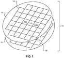
- FIG. 1 is an exploded view of one example of stacked semiconductor dies 102 and 104 of an example stacked imaging system 100 in accordance with the teachings of the present invention.
- semiconductor dies 102 and 104 are stacked device wafers that may include silicon, gallium arsenide, or other suitable semiconductor materials.
- semiconductor die 102 is a sensor die that includes a pixel array 106 having a plurality of pixel cells 110A, 110B, 110C, etc .
- semiconductor die 104 is a logic die that includes corresponding pixel support circuits to support operation of the pixel cells in pixel array 106 in accordance with the teachings of the present invention.
- pixel cells 110A, 110B, and 110C may be shared pixel cells.
- semiconductor die 102, which includes pixel array 106 is stacked with and coupled to semiconductor die 104.
- the plurality of shared pixel cells 110A, 110B, 110C, etc ., of pixel array 106 are coupled to the pixel support circuits 108 through interconnection lines (as will be shown for example in FIG. 2 ) that are coupled between semiconductor die 102 and semiconductor die 104.
- pixel cells 110A, 110B, 110C, etc ., of pixel array 106 are arranged into groupings such that there are shield bumps (as will be shown for example in FIG.
- every other shared pixel cell of two rows of pixel array 106 are read out at a time such that the shared pixel cells are read out simultaneously only along diagonals of the pixel array. Since the shared pixel cells are read out simultaneously only along diagonals of the pixel array 106, there are shield bumps between adjacent shared pixel cells that are being read out along the diagonal of the pixel array.
- the unwanted effects caused by the capacitive coupling between adjacent interconnection lines along the same row of the pixel array can be avoided when reading out pixel data from the pixel array in accordance with the teachings of the present invention.
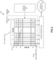
- FIG. 2 is a block diagram illustrating a stacked imaging system 200 in accordance with the teachings of the present invention.
- the stacked imaging system 200 of FIG. 2 may be an example of the stacked imaging system 100 shown in FIG. 1 , and therefore it should be appreciated that similarly named and numbered elements referenced below are coupled and function as described above.
- stacked imaging system 200 includes a first semiconductor die, labeled sensor die 202, that is stacked with and coupled to a second semiconductor die, labeled logic die 204.
- sensor die 202 includes a pixel array 206 arranged into groupings of shared pixels 210, and logic die 204 includes readout circuitry 212 coupled to read out image data from the groupings of shared pixels 210 through interconnections 218.
- logic die 204 also includes function circuitry 214 coupled to the readout circuitry 212, and control circuitry 216 coupled to the pixel array 206.
- pixel array 206 is a two dimensional (2D) pixel array of groupings of shared pixels 210 of an image sensor.
- each shared pixel 210 is a 2x2 shared pixel.
- each shared pixel 210 includes a plurality of photodiodes (e.g ., 4 photodiodes, P1/P2/P3/P4) that share a floating diffusion coupled to an interconnection 218.
- an output bitline is coupled to be read out through each interconnection 218 by the readout circuitry in the logic die 204.
- each photodiode (e.g ., P1/P2/P3/P4) of each shared pixel 210 in pixel array 206 is arranged into a row (e.g ., rows R1 to Ry) and a column ( e.g ., column C1 to Cx) to acquire image data for an image of a person, place, object, etc., which can then be used to render a 2D image of the person, place, object, etc., in accordance with the teachings of the present invention.
- stacked imaging system 200 also includes a plurality of shield bumps 220 that are disposed in corners of the pixel groupings 210.
- the shield bumps may be dummy interconnect lines, power supply lines, ground lines, or the like.
- every other shared pixel cell 210 of two rows of pixel array 206 are read out at a time such that the shared pixel cells 210 are read out simultaneously only along diagonals of the pixel array 206.
- the pixel data is therefore read out from the photodiodes (e.g ., P1/P2/P3/P4) of each shared pixel 210 in pixel array 206 through interconnections 218 to readout circuitry 212, and is then transferred to function circuitry 214.
- readout circuitry 212 may include amplification circuitry, analog-to-digital (ADC) conversion circuitry, or the like.
- Function circuitry 214 may include digital circuitry and may simply store the image data or even manipulate the image data with image signal processing techniques to apply post image effects (e.g., crop, rotate, remove red eye, adjust brightness, adjust contrast, or otherwise).
- control circuitry 216 is coupled to pixel array 206 to control the operational characteristics of pixel array 206.
- control circuitry 216 may generate control signals, such as the transfer gate control signals, as well as for example, reset signals, select signals, shutter signals, and other control signals coupled to pixel array 206 to control image acquisition.
- the shutter signal is a global shutter signal for simultaneously enabling all pixel cells within pixel array 206 to simultaneously capture their respective image data during a single acquisition window.
- the shutter signal is a rolling shutter signal such that each row, column, or group of pixels is sequentially enabled during consecutive acquisition windows.
- FIG. 3 shows one example schematic along a row of shared pixel cells in a pixel array of a stacked imaging system 300 that illustrates the coupling capacitance exists between adjacent interconnection lines along the same row.
- the stacked imaging system 300 of FIG. 3 may be an example of the stacked imaging system 100 shown in FIG. 1 , and/or the stacked imaging system 200 of FIG. 2 , and therefore it should be appreciated that similarly named and numbered elements referenced below are coupled and function as described above.
- stacked imaging system 300 includes a first semiconductor die 302 that is stacked with and coupled to a second semiconductor die 304.
- first shared pixel cell 310A and a second shared pixel cell 310B are included along the same row in first semiconductor die 302, and pixel support circuitry 346A and pixel support circuitry 346B are included in second semiconductor die 304.
- First shared pixel cell 310A is coupled to pixel support circuitry 346A through interconnection line 318A
- second shared pixel cell 310B is coupled to pixel support circuitry 346B through interconnection line 318B.
- first shared pixel 310A is illustrated as including four photodiodes 322A, 324A, 326A, and 328A, which are coupled to a floating diffusion FD 338A through transfer transistors 330A, 332A, 334A, and 336A, respectively.
- incident light is directed into photodiodes 322A, 324A, 326, and 328A to photogenerate image charge.
- the image charge that is photogenerated in photodiodes 322A, 324A, 326A, and 328A is transferred to floating diffusion FD 338A through transfer transistors 330A, 332A, 334A, and 336A in response to transfer control signals TX1A, TX2A, TX3A, and TX4A, respectively.
- the image charge that is transferred to floating diffusion FD 338A is coupled to pixel support circuitry 346A from first semiconductor die 302 to second semiconductor die 304 through interconnection line 318A.
- interconnection line 318A is coupled to a gate terminal of a source follower coupled amplifier transistor 340A, which is coupled to amplify the image data received from the interconnection line 318A.
- the drain terminal of the source follower coupled amplifier transistor 340A is coupled to a supply voltage VDD, and the source terminal is coupled to a row select transistor 342A.
- the image data that is amplified by the source follower coupled amplifier transistor 340A is coupled to an output bitline 344A through row select transistor 342A in response to a row select control signal RSA.
- the output bitline 344A is coupled to be read out through readout circuitry, such as for example readout circuitry 212 of FIG. 2 .
- second shared pixel 310B is illustrated as including four photodiodes 322B, 324B, 326B, and 328B, which are coupled to a floating diffusion FD 338B through transfer transistors 330B, 332B, 334B, and 336B, respectively.
- incident light is also directed into photodiodes 322B, 324B, 326B, and 328B to photogenerate image charge.
- the image charge that is photogenerated in photodiodes 322B, 324B, 326B, and 328A is transferred to floating diffusion FD 338B through transfer transistors 330B, 332B, 334B, and 336B in response to transfer control signals TX1B, TX2B, TX3B, and TX4B, respectively.
- the image charge that is transferred to floating diffusion FD 338B is coupled to pixel support circuitry 346B from first semiconductor die 302 to second semiconductor die 304 through interconnection line 318B.
- interconnection line 318B is coupled to a gate terminal of a source follower coupled amplifier transistor 340B, which is coupled to amplify the image data received from the interconnection line 318B.
- the drain terminal of the source follower coupled amplifier transistor 340B is coupled to supply voltage VDD, and the source terminal is coupled to a row select transistor 342B.
- the image data that is amplified by the source follower coupled amplifier transistor 340B is coupled to an output bitline 344B through row select transistor 342B in response to a row select control signal RSB.
- the output bitline 344B is coupled to be read out through readout circuitry, such as for example readout circuitry 212 of FIG. 2 .
- first shared pixel 310A and second shared pixel 310B are in the same row of a pixel array, such as for example row R1 of pixel array 206 of FIG. 2 .
- the interconnection line 318A that is coupled to shared pixel 310A is adjacent to interconnection line 318B coupled to shared pixel 310B along the same row.
- FIG. 4 is a block diagram illustrating an example pixel array 406 with shield bumps disposed in the corners of the pixel groupings, such that there are shield bumps between the interconnections lines of pixel groupings that are read out simultaneously only along diagonals of the pixel array in accordance with the teachings of the present invention.
- the pixel array 406 of FIG. 4 may be an example of the pixel array 106 shown in FIG. 1 , and/or the pixel array 206 of FIG. 2 , etc., and therefore it should be appreciated that similarly named and numbered elements referenced below are coupled and function as described above.
- pixel array 406 including plurality of pixels cells 410A and 410B that are alternatingly arranged in a checkerboard pattern into a plurality of rows and a plurality of columns as shown.
- the pixel cells are shared pixels including for example four photodiodes, similar to for instance the example described in FIG. 3 .
- pixel array 406 is included in a first semiconductor die that is stacked with and coupled to a semiconductor die that includes pixel support circuitry coupled to pixel array 406 through interconnects in accordance with the teachings of the present invention.
- pixel array 406 also includes a plurality of shield bumps 420, which are disposed proximate to corners of the pixel cells 410A and 410B.
- the shield bumps may be dummy interconnect lines, power supply lines, ground lines, or the like.
- each one of the plurality of shield bumps 410 is disposed between adjacent interconnect lines coupled to the pixel cells 410A and 410B along diagonals of the pixel array 406 in accordance with the teachings of the present invention. To illustrate, the diagonals from the upper left towards the lower right through pixel cells 410A are labeled with dashed lines A-A'.
- each one of the plurality of shield bumps 420 is disposed between adjacent interconnect lines that are coupled to shared pixel cells 410A and 410B along diagonals A-A' or B-B' of the pixel array 406 in accordance with the teachings of the present invention.
- the shield bumps 420 are adapted to shield a coupling capacitance between adjacent interconnect lines that are coupled to pixel cells 410A and 410B along the diagonals A-A' and B-B' of the pixel array 406 in accordance with the teachings of the present invention.
- every other pixel cell 410A, and then remaining every other pixel cell 410B, in two rows at a time of the pixel array 406 are read out such that there is a shield bump 420 disposed between the interconnect lines of the pixel cells from the two rows of the pixel array 406 that are being read out at that time.
- every other pixel cell 410A e.g., along diagonals A-A'
- every other pixel cell 410A e.g., along diagonals A-A'
- every other pixel cell 410B (e.g., along diagonals B-B') of two rows of pixel array 406 are read out simultaneously. Accordingly, there is a shield bump 420 between the interconnection line of each adjacent pixel cell 410B that is being read out to eliminate or substantially reduce the coupling capacitance between the two adjacent interconnection lines along diagonals B-B' in accordance with the teachings of the present invention.
- FIG. 5 is a cross section view of an example stacked imaging system 500 with stacked first and second semiconductor dies including shield bumps disposed in corners of the pixel groupings such that there are shield bumps between the interconnections lines of pixels that are read out simultaneously only along a diagonals of the pixel array in accordance with the teachings of the present invention.
- the stacked imaging system 500 of FIG. 5 may be an example of the stacked imaging system shown in FIG. 1 , and/or the stacked imaging system of FIG. 2 , etc., and therefore it should be appreciated that similarly named and numbered elements referenced below are coupled and function as described above.
- FIG. 5 shows stacked imaging system 500 including a first semiconductor die, which is labeled sensor die 502, that is stacked with and coupled to a second semiconductor die, which is labeled logic die 504.
- the example depicted in FIG. 5 also illustrates interconnections 518 between sensor die 502 and logic die 504, which couple the pixel cells included in the sensor die 502 to the corresponding pixel support circuits in logic die 504 as described above.
- the cross section view of imaging system 500 is along one of the diagonals A-A' or B-B' of pixel array 406 as illustrated in FIG. 4 above.
- shield bumps 520 disposed between adjacent interconnection lines 518 along each of the diagonals A-A' and/or B-B' of the pixel array of stacked imaging system 500 in accordance with the teachings of the present invention.
- a shield bump 520 disposed the corresponding interconnect lines 518 in accordance with the teachings of the present invention.
Landscapes
- Solid State Image Pick-Up Elements (AREA)
- Transforming Light Signals Into Electric Signals (AREA)
Abstract
Description
- This invention is related to image sensors. In particular, embodiments of the present invention are related to stacked image sensors.
- Image sensors have become ubiquitous. They are widely used in digital cameras, cellular phones, security cameras, as well as, medical, automobile, and other applications. The technology used to manufacture image sensors, and in particular, complementary metal-oxide-semiconductor (CMOS) image sensors, has continued to advance at great pace. For example, the demands of higher resolution and lower power consumption have encouraged the further miniaturization and integration of these image sensors.
- In conventional stacked image sensors, the photodiodes of pixels are typically on a first die, and the pixel support circuits are on a second die that is stacked together with the first die that includes the photodiodes. Interconnection lines are provided between the first and second dies in order to provide electrical connections between the photodiodes on the first die and the corresponding pixel support circuits on the second die.
- One of the challenges presented with conventional stacked image sensors is the unwanted capacitive coupling that exists between the adjacent interconnection lines between the first and second dies of the stacked image sensors that connect the photodiodes to the pixel support circuits. The capacitive coupling between the adjacent interconnection lines can cause interference or result in other unwanted consequences between adjacent interconnection lines when reading out image data from the photodiodes.
- Non-limiting and non-exhaustive embodiments of the present invention are described with reference to the following figures, wherein like reference numerals refer to like parts throughout the various views unless otherwise specified.
-
FIG. 1 is an exploded view of one example of a stacked imaging system including stacked semiconductor device wafers providing a stacked image sensor with shield bumps between interconnections along the diagonals of the image sensor in accordance with the teachings of the present invention. -
FIG. 2 is a block diagram illustrating an imaging system implemented as a stacked image sensor including a pixel array having shared pixel cells arranged in a first semiconductor die that are coupled through interconnections to pixel support circuits in a second semiconductor die with shield bumps between the interconnections along the diagonals of the pixel array in accordance with the teachings of the present invention. -
FIG. 3 shows one example schematic along a row of pixels in a pixel array of a stacked image sensor in which there is a coupling capacitance between adjacent interconnection lines along the rows of the pixel array in accordance with the teachings of the present invention. -
FIG. 4 is a block diagram illustrating an example pixel array with shield bumps disposed in corners of the pixel groupings such that there are shield bumps between the interconnections lines of pixel groupings that are read out simultaneously along diagonals of the pixel array in accordance with the teachings of the present invention. -
FIG. 5 is a cross section view of an example stacked imaging system with stacked first and second semiconductor dies including shield bumps disposed in corners of the pixel groupings such that there are shield bumps between the interconnections lines of pixel groupings that are read out simultaneously along a diagonals of the pixel array in accordance with the teachings of the present invention. - Corresponding reference characters indicate corresponding components throughout the several views of the drawings. Skilled artisans will appreciate that elements in the figures are illustrated for simplicity and clarity and have not necessarily been drawn to scale. For example, the dimensions of some of the elements in the figures may be exaggerated relative to other elements to help to improve understanding of various embodiments of the present invention. Also, common but well-understood elements that are useful or necessary in a commercially feasible embodiment are often not depicted in order to facilitate a less obstructed view of these various embodiments of the present invention.
- In the following description numerous specific details are set forth to provide a thorough understanding of the embodiments. One skilled in the relevant art will recognize, however, that the techniques described herein can be practiced without one or more of the specific details, or with other methods, components, materials, etc. In other instances, well-known structures, materials, or operations are not shown or described in detail to avoid obscuring certain aspects.
- Reference throughout this specification to "one embodiment" or "an embodiment" means that a particular feature, structure, or characteristic described in connection with the embodiment is included in at least one embodiment of the present invention. Thus, the appearances of the phrases "in one embodiment" or "in an embodiment" in various places throughout this specification are not necessarily all referring to the same embodiment. Furthermore, the particular features, structures, or characteristics may be combined in any suitable manner in one or more embodiments.
- Throughout this specification, several terms of art are used. These terms are to take on their ordinary meaning in the art from which they come, unless specifically defined herein or the context of their use would clearly suggest otherwise. For example, the term "or" is used in the inclusive sense (e.g., as in "and/or") unless the context clearly indicates otherwise. It should be noted that element names and symbols may be used interchangeably through this document (e.g., Si vs. silicon); however, both have identical meaning.
- As will be shown, an example of a stacked image sensor in accordance with the teachings of the present invention includes a two dimensional array of pixels arranged in a first semiconductor die that are coupled through interconnect lines to pixel support circuitry disposed in a second semiconductor die that is stacked with the first semiconductor die. In various examples, the pixels may be arranged in groupings, such as shared pixel cells. For instance, the pixels are arranged into groupings such that there are shield bumps disposed in the interconnect layer in the corners of the groupings of the shared pixel cells. In various examples, the shield bumps may be dummy interconnect lines, power supply lines, ground lines, or the like. As such, there are shield bumps between the interconnections lines of the shared pixel cells to the pixel support circuitry, which are read out simultaneously along diagonals of the pixel array in accordance with the teachings of the present invention.
- For instance, as will be disclosed in one example of a readout scheme in accordance with the teachings of the present invention, every other shared pixel cell of two rows of shared pixel cells of the pixel array are read out at a time such that the shared pixel cells are read out simultaneously along diagonals of the pixel array. Since the shared pixel cells are read out simultaneously along diagonals of the pixel array, there are shield bumps between adjacent shared pixel cells that are being read out along the diagonal of the pixel array. With the shielding provided by the shield bumps in the corners of the pixel groupings, the unwanted effects caused by the capacitive coupling between adjacent interconnection lines along a row of the pixel array can be avoided when reading out pixel data from the pixel array in accordance with the teachings of the present invention.
- To illustrate,
FIG. 1 is an exploded view of one example of stacked semiconductor dies 102 and 104 of an example stackedimaging system 100 in accordance with the teachings of the present invention. In various examples, semiconductor dies 102 and 104 are stacked device wafers that may include silicon, gallium arsenide, or other suitable semiconductor materials. In the illustrated example, semiconductor die 102 is a sensor die that includes apixel array 106 having a plurality ofpixel cells semiconductor die 104 is a logic die that includes corresponding pixel support circuits to support operation of the pixel cells inpixel array 106 in accordance with the teachings of the present invention. In one example,pixel cells semiconductor die 102, which includespixel array 106, is stacked with and coupled to semiconductor die 104. - As will be discussed in more detail below, the plurality of shared
pixel cells pixel array 106 are coupled to thepixel support circuits 108 through interconnection lines (as will be shown for example inFIG. 2 ) that are coupled between semiconductor die 102 andsemiconductor die 104. As will be shown,pixel cells pixel array 106 are arranged into groupings such that there are shield bumps (as will be shown for example inFIG. 2 ) disposed in the interconnect layer in the corners of the groupings of sharedpixel cells pixel cells pixel array 106 to thepixel support circuits 108. In various examples, every other shared pixel cell of two rows ofpixel array 106 are read out at a time such that the shared pixel cells are read out simultaneously only along diagonals of the pixel array. Since the shared pixel cells are read out simultaneously only along diagonals of thepixel array 106, there are shield bumps between adjacent shared pixel cells that are being read out along the diagonal of the pixel array. With the shielding provided by the shield bumps in the corners of the pixel groupings, the unwanted effects caused by the capacitive coupling between adjacent interconnection lines along the same row of the pixel array can be avoided when reading out pixel data from the pixel array in accordance with the teachings of the present invention. - To illustrate,
FIG. 2 is a block diagram illustrating astacked imaging system 200 in accordance with the teachings of the present invention. It is noted that thestacked imaging system 200 ofFIG. 2 may be an example of thestacked imaging system 100 shown inFIG. 1 , and therefore it should be appreciated that similarly named and numbered elements referenced below are coupled and function as described above. For instance, in one example, stackedimaging system 200 includes a first semiconductor die, labeled sensor die 202, that is stacked with and coupled to a second semiconductor die, labeled logic die 204. In one example, sensor die 202 includes apixel array 206 arranged into groupings of sharedpixels 210, and logic die 204 includesreadout circuitry 212 coupled to read out image data from the groupings of sharedpixels 210 throughinterconnections 218. In the depicted example,logic die 204 also includesfunction circuitry 214 coupled to thereadout circuitry 212, andcontrol circuitry 216 coupled to thepixel array 206. - As shown in the example illustrated in
FIG. 2 ,pixel array 206 is a two dimensional (2D) pixel array of groupings of sharedpixels 210 of an image sensor. For instance, in the example illustrated inFIG. 2 , each sharedpixel 210 is a 2x2 shared pixel. In the example, each sharedpixel 210 includes a plurality of photodiodes (e.g., 4 photodiodes, P1/P2/P3/P4) that share a floating diffusion coupled to aninterconnection 218. In the depicted example, an output bitline is coupled to be read out through eachinterconnection 218 by the readout circuitry in thelogic die 204. As illustrated, each photodiode (e.g., P1/P2/P3/P4) of each sharedpixel 210 inpixel array 206 is arranged into a row (e.g., rows R1 to Ry) and a column (e.g., column C1 to Cx) to acquire image data for an image of a person, place, object, etc., which can then be used to render a 2D image of the person, place, object, etc., in accordance with the teachings of the present invention. - As shown in the depicted example, stacked
imaging system 200 also includes a plurality ofshield bumps 220 that are disposed in corners of thepixel groupings 210. In various examples, the shield bumps may be dummy interconnect lines, power supply lines, ground lines, or the like. As such, there areshield bumps 220 between theinterconnections lines 218 of the sharedpixels 210 that are read out simultaneously only along diagonals of thepixel array 206 in accordance with the teachings of the present invention. Stated in another way, every other sharedpixel cell 210 of two rows ofpixel array 206 are read out at a time such that the sharedpixel cells 210 are read out simultaneously only along diagonals of thepixel array 206. Since the sharedpixel cells 210 are read out simultaneously along diagonals of thepixel array 206, there areshield bumps 220 between adjacent sharedpixel cells 210 that are being read out along the diagonal of thepixel array 206. With the shielding provided by the shield bumps 220 in the corners of thepixel groupings 210, the unwanted effects caused by the capacitive coupling between adjacent interconnection lines along the same row of thepixel array 206 can be avoided when reading out pixel data from thepixel array 206 in accordance with the teachings of the present invention. - The pixel data is therefore read out from the photodiodes (e.g., P1/P2/P3/P4) of each shared
pixel 210 inpixel array 206 throughinterconnections 218 toreadout circuitry 212, and is then transferred to functioncircuitry 214. In various examples,readout circuitry 212 may include amplification circuitry, analog-to-digital (ADC) conversion circuitry, or the like.Function circuitry 214 may include digital circuitry and may simply store the image data or even manipulate the image data with image signal processing techniques to apply post image effects (e.g., crop, rotate, remove red eye, adjust brightness, adjust contrast, or otherwise). - As mentioned,
control circuitry 216 is coupled topixel array 206 to control the operational characteristics ofpixel array 206. For example,control circuitry 216 may generate control signals, such as the transfer gate control signals, as well as for example, reset signals, select signals, shutter signals, and other control signals coupled topixel array 206 to control image acquisition. In one example, the shutter signal is a global shutter signal for simultaneously enabling all pixel cells withinpixel array 206 to simultaneously capture their respective image data during a single acquisition window. In another example, the shutter signal is a rolling shutter signal such that each row, column, or group of pixels is sequentially enabled during consecutive acquisition windows. -
FIG. 3 shows one example schematic along a row of shared pixel cells in a pixel array of astacked imaging system 300 that illustrates the coupling capacitance exists between adjacent interconnection lines along the same row. It is noted that thestacked imaging system 300 ofFIG. 3 may be an example of the stackedimaging system 100 shown inFIG. 1 , and/or the stackedimaging system 200 ofFIG. 2 , and therefore it should be appreciated that similarly named and numbered elements referenced below are coupled and function as described above. For instance, as shown in the illustration, stackedimaging system 300 includes a first semiconductor die 302 that is stacked with and coupled to a second semiconductor die 304. In the depicted example, a first sharedpixel cell 310A and a second sharedpixel cell 310B are included along the same row in first semiconductor die 302, andpixel support circuitry 346A andpixel support circuitry 346B are included in second semiconductor die 304. First sharedpixel cell 310A is coupled topixel support circuitry 346A through interconnection line 318A, and second sharedpixel cell 310B is coupled topixel support circuitry 346B through interconnection line 318B. - As shown in the depicted example, first shared
pixel 310A is illustrated as including fourphotodiodes 322A, 324A, 326A, and 328A, which are coupled to a floatingdiffusion FD 338A throughtransfer transistors 330A, 332A, 334A, and 336A, respectively. In operation, incident light is directed into photodiodes 322A, 324A, 326, and 328A to photogenerate image charge. The image charge that is photogenerated inphotodiodes 322A, 324A, 326A, and 328A is transferred to floatingdiffusion FD 338A throughtransfer transistors 330A, 332A, 334A, and 336A in response to transfer control signals TX1A, TX2A, TX3A, and TX4A, respectively. In the example, the image charge that is transferred to floatingdiffusion FD 338A is coupled topixel support circuitry 346A from first semiconductor die 302 to second semiconductor die 304 through interconnection line 318A. In particular, as shown in the depicted example, interconnection line 318A is coupled to a gate terminal of a source follower coupledamplifier transistor 340A, which is coupled to amplify the image data received from the interconnection line 318A. In the example, the drain terminal of the source follower coupledamplifier transistor 340A is coupled to a supply voltage VDD, and the source terminal is coupled to a rowselect transistor 342A. The image data that is amplified by the source follower coupledamplifier transistor 340A is coupled to anoutput bitline 344A through rowselect transistor 342A in response to a row select control signal RSA. In one example, theoutput bitline 344A is coupled to be read out through readout circuitry, such as forexample readout circuitry 212 ofFIG. 2 . - Similarly, as further shown in the depicted example of
FIG. 3 , second sharedpixel 310B is illustrated as including fourphotodiodes diffusion FD 338B throughtransfer transistors 330B, 332B, 334B, and 336B, respectively. In operation, incident light is also directed intophotodiodes photodiodes diffusion FD 338B throughtransfer transistors 330B, 332B, 334B, and 336B in response to transfer control signals TX1B, TX2B, TX3B, and TX4B, respectively. In the example, the image charge that is transferred to floatingdiffusion FD 338B is coupled topixel support circuitry 346B from first semiconductor die 302 to second semiconductor die 304 through interconnection line 318B. In particular, as shown in the depicted example, interconnection line 318B is coupled to a gate terminal of a source follower coupledamplifier transistor 340B, which is coupled to amplify the image data received from the interconnection line 318B. In the example, the drain terminal of the source follower coupledamplifier transistor 340B is coupled to supply voltage VDD, and the source terminal is coupled to a rowselect transistor 342B. The image data that is amplified by the source follower coupledamplifier transistor 340B is coupled to anoutput bitline 344B through rowselect transistor 342B in response to a row select control signal RSB. In one example, theoutput bitline 344B is coupled to be read out through readout circuitry, such as forexample readout circuitry 212 ofFIG. 2 . - As mentioned, it is appreciated that the first shared
pixel 310A and second sharedpixel 310B are in the same row of a pixel array, such as for example row R1 ofpixel array 206 ofFIG. 2 . As such, the interconnection line 318A that is coupled to sharedpixel 310A is adjacent to interconnection line 318B coupled to sharedpixel 310B along the same row. Furthermore, there is no shield bump between interconnection line 318A and adjacent interconnection line 318B. Since there is an absence of a shield bump between interconnection line 318A and interconnection line 318B, there is instead anunwanted coupling capacitance 320 between interconnection line 318A and interconnection line 318B, which causes unwanted interference when reading out image data from first sharedpixel cell 310A and second sharedpixel cell 310B. -
FIG. 4 is a block diagram illustrating anexample pixel array 406 with shield bumps disposed in the corners of the pixel groupings, such that there are shield bumps between the interconnections lines of pixel groupings that are read out simultaneously only along diagonals of the pixel array in accordance with the teachings of the present invention. It is noted that thepixel array 406 ofFIG. 4 may be an example of thepixel array 106 shown inFIG. 1 , and/or thepixel array 206 ofFIG. 2 , etc., and therefore it should be appreciated that similarly named and numbered elements referenced below are coupled and function as described above. In particular, the example depicted inFIG. 4 showspixel array 406 including plurality ofpixels cells FIG. 3 . In the example,pixel array 406 is included in a first semiconductor die that is stacked with and coupled to a semiconductor die that includes pixel support circuitry coupled topixel array 406 through interconnects in accordance with the teachings of the present invention. - As shown in the depicted example,
pixel array 406 also includes a plurality of shield bumps 420, which are disposed proximate to corners of thepixel cells pixel cells pixel array 406 in accordance with the teachings of the present invention. To illustrate, the diagonals from the upper left towards the lower right throughpixel cells 410A are labeled with dashed lines A-A'. Similarly, the diagonals from the lower left towards the upper right thorughpixel cells 410B are labeled with dashed lines B-B'. Therefore, each one of the plurality of shield bumps 420 is disposed between adjacent interconnect lines that are coupled to sharedpixel cells pixel array 406 in accordance with the teachings of the present invention. - In operation, the shield bumps 420 are adapted to shield a coupling capacitance between adjacent interconnect lines that are coupled to
pixel cells pixel array 406 in accordance with the teachings of the present invention. Thus, in one example, during read out ofpixel array 406, everyother pixel cell 410A, and then remaining everyother pixel cell 410B, in two rows at a time of thepixel array 406 are read out such that there is ashield bump 420 disposed between the interconnect lines of the pixel cells from the two rows of thepixel array 406 that are being read out at that time. - For example, during a first read out pass, every
other pixel cell 410A (e.g., along diagonals A-A') of two rows ofpixel array 406 are read out simultaneously. Accordingly, there is ashield bump 420 between the interconnection line of eachadjacent pixel cell 410A that is being read out to eliminate or substantially reduce the coupling capacitance between the two adjacent interconnection lines along diagonals A-A' in accordance with the teachings of the present invention. - Subsequently, during a next read out pass, every
other pixel cell 410B (e.g., along diagonals B-B') of two rows ofpixel array 406 are read out simultaneously. Accordingly, there is ashield bump 420 between the interconnection line of eachadjacent pixel cell 410B that is being read out to eliminate or substantially reduce the coupling capacitance between the two adjacent interconnection lines along diagonals B-B' in accordance with the teachings of the present invention. -
FIG. 5 is a cross section view of an example stackedimaging system 500 with stacked first and second semiconductor dies including shield bumps disposed in corners of the pixel groupings such that there are shield bumps between the interconnections lines of pixels that are read out simultaneously only along a diagonals of the pixel array in accordance with the teachings of the present invention. It is noted that thestacked imaging system 500 ofFIG. 5 may be an example of the stacked imaging system shown inFIG. 1 , and/or the stacked imaging system ofFIG. 2 , etc., and therefore it should be appreciated that similarly named and numbered elements referenced below are coupled and function as described above. - In particular, the example depicted in
FIG. 5 shows stackedimaging system 500 including a first semiconductor die, which is labeled sensor die 502, that is stacked with and coupled to a second semiconductor die, which is labeled logic die 504. The example depicted inFIG. 5 also illustrates interconnections 518 between sensor die 502 and logic die 504, which couple the pixel cells included in the sensor die 502 to the corresponding pixel support circuits in logic die 504 as described above. In the example, it is appreciated that the cross section view ofimaging system 500 is along one of the diagonals A-A' or B-B' ofpixel array 406 as illustrated inFIG. 4 above. As such, there are also shieldbumps 520 disposed between adjacent interconnection lines 518 along each of the diagonals A-A' and/or B-B' of the pixel array of stackedimaging system 500 in accordance with the teachings of the present invention. As such, when every other pixel cell in two rows of the pixel array included instacked imaging system 500 are read out at a time, there is ashield bump 520 disposed the corresponding interconnect lines 518 in accordance with the teachings of the present invention. With a shield bump 518 disposed between adjacent interconnection lines 518, the coupling capacitance is eliminated to reduce unwanted interference, crosstalk, and the like, during readouts ofstacked image sensor 500 in accordance with the teachings of the present invention. - The above description of illustrated embodiments of the invention, including what is described in the Abstract, is not intended to be exhaustive or to limit the invention to the precise forms disclosed. While specific embodiments of, and examples for, the invention are described herein for illustrative purposes, various modifications are possible within the scope of the invention, as those skilled in the relevant art will recognize.
- These modifications can be made to the invention in light of the above detailed description. The terms used in the following claims should not be construed to limit the invention to the specific embodiments disclosed in the specification. Rather, the scope of the invention is to be determined entirely by the following claims, which are to be construed in accordance with established doctrines of claim interpretation.
- The following statements provide general expressions of the disclosure herein:
- A1. An image sensor, comprising:
- a pixel array including plurality of pixel cells arranged into a plurality of rows and a plurality of columns of pixel cells in a first semiconductor die;
- a plurality of pixel support circuits arranged in a second semiconductor die, wherein the first and second semiconductor dies are stacked and coupled together;
- a plurality of interconnect lines coupled between the first and second semiconductor dies, wherein each one of the plurality of pixel cells is coupled to a corresponding one of the plurality of pixel support circuits through a corresponding one plurality of interconnect lines; and
- a plurality of shield bumps disposed proximate to corners of the pixel cells and between the first and second semiconductor dies such that each one of the plurality of shield bumps is disposed between adjacent interconnect lines along a diagonal of the pixel array.
- A2. The image sensor of statement A1, wherein each one of the plurality of shield bumps is disposed between adjacent interconnect lines along the diagonal of the pixel array is adapted to shield a coupling capacitance between said adjacent interconnect lines along the diagonal of the pixel array.
- A3. The image sensor of any previous statement, wherein every other pixel cell in two rows of the pixel array are read out at a time such that there is said one of the plurality of shield bumps disposed between said interconnect lines that are coupled to said every other pixel cell in said two rows of the pixel array that are read out at the time.
- A4. The image sensor of any previous statement, wherein each one of the plurality of shield bumps is one of a dummy interconnect line, a power supply line, or a ground line.
- A5. The image sensor of any previous statement, wherein each one of the plurality of pixel cells comprises a photodiode disposed in first semiconductor die and coupled to the corresponding interconnect line coupled to said one of the plurality of pixel cells.
- A6. The image sensor of statement A5, wherein each one of the plurality of pixel cells further comprises a transfer transistor disposed in the first semiconductor die and coupled between said photodiode and the corresponding interconnect line coupled to said one of the plurality of pixel cells.
- A7. The image sensor of any previous statement, wherein each one of the plurality of pixel cells is a shared pixel comprising a plurality of photodiodes disposed in the first semiconductor die and coupled to the corresponding interconnect line coupled to said one of the plurality of pixel cells.
- A8. The image sensor of statement A7, wherein each shared pixel further comprises a plurality of transfer transistors, wherein each one of the plurality of transfer transistors is disposed in the first semiconductor die and coupled between one of the plurality of photodiodes and the corresponding interconnect line coupled to said one of the plurality of pixel cells.
- A9. The image sensor of any previous statement, wherein each one of the pixel support circuits comprises:
- an amplifier transistor disposed in second semiconductor die and coupled to the corresponding interconnect line coupled to said one of the plurality of pixel cells; and
- a row select transistor disposed in second semiconductor die and coupled between an output of the amplifier transistor and an output bitline.
- A10. An imaging system, comprising:
- a sensor wafer including a first semiconductor layer, wherein the sensor wafer includes a pixel array including plurality of pixel cells arranged into a plurality of rows and a plurality of columns of pixel cells in a first semiconductor layer;
- a logic wafer including a second semiconductor layer, wherein the logic wafer includes a plurality of pixel support circuits arranged in a second semiconductor layer, wherein the sensor wafer and the logic wafer are stacked and coupled together;
- a plurality of interconnect lines coupled between the pixel array and the plurality of pixel support circuits, wherein each one of the plurality of pixel cells in the sensor wafer is coupled to a corresponding one of the plurality of pixel support circuits in the logic wafer through a corresponding one plurality of interconnect lines; and
- a plurality of shield bumps disposed proximate to corners of the pixel cells and between the sensor wafer and logic wafer such that each one of the plurality of shield bumps is disposed between adjacent interconnect lines along a diagonal of the pixel array.
- A11. The imaging system of statement A10, wherein the logic wafer further includes:
- control circuitry disposed in the second semiconductor layer and coupled to the pixel array to control operation of the pixel array;
- readout circuitry disposed in the second semiconductor layer and coupled to the plurality of pixel support circuits to readout image data from the pixel array; and
- function circuitry disposed in the second semiconductor layer and coupled to the readout circuitry to store the image data readout from the pixel array.
- A12. The imaging system of statement A10 or A11, wherein each one of the plurality of shield bumps is disposed between adjacent interconnect lines along the diagonal of the pixel array is adapted to shield a coupling capacitance between said adjacent interconnect lines along the diagonal of the pixel array.
- A13. The imaging system of statement A12, wherein every other pixel cell in two rows of the pixel array are read out at a time such that there is said one of the plurality of shield bumps disposed between said interconnect lines along the diagonal that are coupled to said every other pixel cell in said two rows of the pixel array that are read out at the time.
- A14. The imaging system of any of statements A10 to A13, wherein each one of the plurality of shield bumps is one of a dummy interconnect line, a power supply line, or a ground line.
- A15. The imaging system of any of statements A10 to A14, wherein each one of the plurality of pixel cells comprises a photodiode disposed in first semiconductor layer and coupled to the corresponding interconnect line coupled to said one of the plurality of pixel cells.
- A16. The imaging system of statement A15, wherein each one of the plurality of pixel cells further comprises a transfer transistor disposed in the first semiconductor layer and coupled between said photodiode and the corresponding interconnect line coupled to said one of the plurality of pixel cells.
- A17. The imaging system of any of statements A10 to A16, wherein each one of the plurality of pixel cells is a shared pixel comprising a plurality of photodiodes disposed in the first semiconductor layer and coupled to the corresponding interconnect line coupled to said one of the plurality of pixel cells.
- A18. The imaging system of statement A17, wherein each shared pixel further comprises a plurality of transfer transistors, wherein each one of the plurality of transfer transistors is disposed in the first semiconductor layer and coupled between one of the plurality of photodiodes and the corresponding interconnect line coupled to said one of the plurality of pixel cells.
- A19. The imaging system of any of statements A10 to A18, wherein each one of the pixel support circuits comprises:
- an amplifier transistor disposed in second semiconductor die and coupled to the corresponding interconnect line coupled to said one of the plurality of pixel cells; and
- a row select transistor disposed in second semiconductor die and coupled between an output of the amplifier transistor and an output bitline.
Claims (11)
- An image sensor, comprising:a pixel array including plurality of pixel cells arranged into a plurality of rows and a plurality of columns of pixel cells in a first semiconductor die;a plurality of pixel support circuits arranged in a second semiconductor die, wherein the first and second semiconductor dies are stacked and coupled together;a plurality of interconnect lines coupled between the first and second semiconductor dies, wherein each one of the plurality of pixel cells is coupled to a corresponding one of the plurality of pixel support circuits through a corresponding one plurality of interconnect lines; anda plurality of shield bumps disposed proximate to corners of the pixel cells and between the first and second semiconductor dies such that each one of the plurality of shield bumps is disposed between adjacent interconnect lines along a diagonal of the pixel array.
- The image sensor of claim 1, wherein each one of the plurality of shield bumps is disposed between adjacent interconnect lines along the diagonal of the pixel array is adapted to shield a coupling capacitance between said adjacent interconnect lines along the diagonal of the pixel array.
- The image sensor of claim 1 or claim 2, wherein every other pixel cell in two rows of the pixel array are read out at a time such that there is said one of the plurality of shield bumps disposed between said interconnect lines that are coupled to said every other pixel cell in said two rows of the pixel array that are read out at the time.
- The image sensor of any previous claim, wherein each one of the plurality of shield bumps is one of a dummy interconnect line, a power supply line, or a ground line.
- The image sensor of any previous claim, wherein each one of the plurality of pixel cells comprises a photodiode disposed in first semiconductor die and coupled to the corresponding interconnect line coupled to said one of the plurality of pixel cells.
- The image sensor of claim 5, wherein each one of the plurality of pixel cells further comprises a transfer transistor disposed in the first semiconductor die and coupled between said photodiode and the corresponding interconnect line coupled to said one of the plurality of pixel cells.
- The image sensor of any previous claim, wherein each one of the plurality of pixel cells is a shared pixel comprising a plurality of photodiodes disposed in the first semiconductor die and coupled to the corresponding interconnect line coupled to said one of the plurality of pixel cells.
- The image sensor of any previous claim, wherein each shared pixel further comprises a plurality of transfer transistors, wherein each one of the plurality of transfer transistors is disposed in the first semiconductor die and coupled between one of the plurality of photodiodes and the corresponding interconnect line coupled to said one of the plurality of pixel cells.
- The image sensor of any previous claim, wherein each one of the pixel support circuits comprises:an amplifier transistor disposed in second semiconductor die and coupled to the corresponding interconnect line coupled to said one of the plurality of pixel cells; anda row select transistor disposed in second semiconductor die and coupled between an output of the amplifier transistor and an output bitline.
- An imaging system, comprising:an image sensor according to any previous claim;a sensor wafer including the pixel array of the image sensor;a logic wafer including the plurality of pixel support circuits of the image sensor, wherein the sensor wafer and the logic wafer are stacked and coupled together.
- The imaging system of claim 10, wherein the logic wafer further includes:control circuitry disposed in the second semiconductor die and coupled to the pixel array to control operation of the pixel array;readout circuitry disposed in the second semiconductor die and coupled to the plurality of pixel support circuits to readout image data from the pixel array; andfunction circuitry disposed in the second semiconductor die and coupled to the readout circuitry to store the image data readout from the pixel array.
Applications Claiming Priority (1)
| Application Number | Priority Date | Filing Date | Title |
|---|---|---|---|
| US15/284,961 US10062722B2 (en) | 2016-10-04 | 2016-10-04 | Stacked image sensor with shield bumps between interconnects |
Publications (2)
| Publication Number | Publication Date |
|---|---|
| EP3306666A1 true EP3306666A1 (en) | 2018-04-11 |
| EP3306666B1 EP3306666B1 (en) | 2022-06-22 |
Family
ID=59923301
Family Applications (1)
| Application Number | Title | Priority Date | Filing Date |
|---|---|---|---|
| EP17192064.8A Active EP3306666B1 (en) | 2016-10-04 | 2017-09-20 | Stacked image sensor with shield bumps between interconnects |
Country Status (4)
| Country | Link |
|---|---|
| US (1) | US10062722B2 (en) |
| EP (1) | EP3306666B1 (en) |
| CN (1) | CN107895731B (en) |
| TW (1) | TWI654753B (en) |
Cited By (1)
| Publication number | Priority date | Publication date | Assignee | Title |
|---|---|---|---|---|
| WO2020100806A1 (en) * | 2018-11-16 | 2020-05-22 | Sony Semiconductor Solutions Corporation | Imaging device |
Families Citing this family (3)
| Publication number | Priority date | Publication date | Assignee | Title |
|---|---|---|---|---|
| KR102591627B1 (en) | 2018-08-17 | 2023-10-20 | 삼성전자주식회사 | Image sensor |
| TWI861140B (en) * | 2019-06-26 | 2024-11-11 | 日商索尼半導體解決方案公司 | Camera |
| US12256162B2 (en) * | 2022-10-05 | 2025-03-18 | Semiconductor Components Industries, Llc | Reference pixel column readout |
Citations (4)
| Publication number | Priority date | Publication date | Assignee | Title |
|---|---|---|---|---|
| JPH04280677A (en) * | 1991-03-08 | 1992-10-06 | Sony Corp | Laminated type solid-state image pickup device |
| US20100060764A1 (en) * | 2008-09-09 | 2010-03-11 | Mccarten John P | High gain read circuit for 3d integrated pixel |
| EP2525406A1 (en) * | 2011-05-20 | 2012-11-21 | Société Française de Détecteurs Infrarouges - SOFRADIR | Low-flow, low-noise detection circuit |
| US20160173803A1 (en) * | 2013-09-18 | 2016-06-16 | Olympus Corporation | Semiconductor device |
Family Cites Families (10)
| Publication number | Priority date | Publication date | Assignee | Title |
|---|---|---|---|---|
| US5760431A (en) * | 1995-11-29 | 1998-06-02 | Massachusetts Institute Of Technology | Multidirectional transfer charge-coupled device |
| US7145143B2 (en) * | 2002-03-18 | 2006-12-05 | Honeywell International Inc. | Tunable sensor |
| US7217601B1 (en) * | 2002-10-23 | 2007-05-15 | Massachusetts Institute Of Technology | High-yield single-level gate charge-coupled device design and fabrication |
| TWI422020B (en) * | 2008-12-08 | 2014-01-01 | Sony Corp | Solid-state imaging device |
| US8089036B2 (en) * | 2009-04-30 | 2012-01-03 | Omnivision Technologies, Inc. | Image sensor with global shutter and in pixel storage transistor |
| TWI467746B (en) | 2010-12-15 | 2015-01-01 | 新力股份有限公司 | Semiconductor device, manufacturing method thereof, and electronic apparatus |
| US9041842B2 (en) * | 2013-07-12 | 2015-05-26 | Omnivision Technologies, Inc. | Image sensor pixel cell readout architecture |
| US11335721B2 (en) * | 2013-11-06 | 2022-05-17 | Taiwan Semiconductor Manufacturing Co., Ltd. | Backside illuminated image sensor device with shielding layer |
| US9419044B2 (en) * | 2014-04-17 | 2016-08-16 | Omnivision Technologies, Inc. | Image sensor pixel having storage gate implant with gradient profile |
| CN105355621B (en) * | 2015-11-26 | 2018-05-29 | 上海集成电路研发中心有限公司 | A kind of stack imaging sensor |
-
2016
- 2016-10-04 US US15/284,961 patent/US10062722B2/en active Active
-
2017
- 2017-09-20 EP EP17192064.8A patent/EP3306666B1/en active Active
- 2017-09-29 CN CN201710906263.2A patent/CN107895731B/en active Active
- 2017-10-03 TW TW106134112A patent/TWI654753B/en active
Patent Citations (4)
| Publication number | Priority date | Publication date | Assignee | Title |
|---|---|---|---|---|
| JPH04280677A (en) * | 1991-03-08 | 1992-10-06 | Sony Corp | Laminated type solid-state image pickup device |
| US20100060764A1 (en) * | 2008-09-09 | 2010-03-11 | Mccarten John P | High gain read circuit for 3d integrated pixel |
| EP2525406A1 (en) * | 2011-05-20 | 2012-11-21 | Société Française de Détecteurs Infrarouges - SOFRADIR | Low-flow, low-noise detection circuit |
| US20160173803A1 (en) * | 2013-09-18 | 2016-06-16 | Olympus Corporation | Semiconductor device |
Cited By (1)
| Publication number | Priority date | Publication date | Assignee | Title |
|---|---|---|---|---|
| WO2020100806A1 (en) * | 2018-11-16 | 2020-05-22 | Sony Semiconductor Solutions Corporation | Imaging device |
Also Published As
| Publication number | Publication date |
|---|---|
| CN107895731A (en) | 2018-04-10 |
| TW201830680A (en) | 2018-08-16 |
| CN107895731B (en) | 2019-10-25 |
| TWI654753B (en) | 2019-03-21 |
| EP3306666B1 (en) | 2022-06-22 |
| US20180097030A1 (en) | 2018-04-05 |
| US10062722B2 (en) | 2018-08-28 |
Similar Documents
| Publication | Publication Date | Title |
|---|---|---|
| US10825854B2 (en) | Stacked photo sensor assembly with pixel level interconnect | |
| US9602750B2 (en) | Image sensor pixels having built-in variable gain feedback amplifier circuitry | |
| US9955091B1 (en) | High dynamic range image sensor read out architecture using in-frame multi-bit exposure control | |
| US9344658B2 (en) | Negative biased substrate for pixels in stacked image sensors | |
| US10536658B2 (en) | Image sensor having stacked imaging and digital wafers where the digital wafer has stacked capacitors and logic circuitry | |
| US9848140B2 (en) | Horizontal banding reduction with ramp generator isolation in an image sensor | |
| US20070018267A1 (en) | Anti-blooming storage pixel | |
| US20170324916A1 (en) | Optical sensor, signal reading method therefor, solid-state imaging device, and signal reading method therefor | |
| US20120007157A1 (en) | Image sensor with compact pixel layout | |
| US20140103411A1 (en) | Stacked chip image sensor with light-sensitive circuit elements on the bottom chip | |
| US20120314109A1 (en) | Solid-state imaging device and camera | |
| US7541628B2 (en) | Image sensors including active pixel sensor arrays | |
| KR102268707B1 (en) | Image sensor | |
| US10854649B2 (en) | Image sensor including unit pixel block having common selection transistor | |
| CN103117289A (en) | Solid-state imaging element, manufacturing method, and electronic device | |
| US10535695B2 (en) | Stacked wafer arrangement for global shutter pixels utilizing capacitive deep trench isolations | |
| EP3306666B1 (en) | Stacked image sensor with shield bumps between interconnects | |
| US11961855B2 (en) | Image sensing device | |
| US7667183B2 (en) | Image sensor with high fill factor pixels and method for forming an image sensor | |
| CN111149351B (en) | Solid-state imaging element and solid-state imaging device | |
| US11290674B1 (en) | Column amplifier capacitor switch circuit to adjust analog gain | |
| US11595597B2 (en) | Image sensing device | |
| US20160099283A1 (en) | Photosensor with channel region having center contact | |
| CN110970453B (en) | Camera device | |
| US9923024B1 (en) | CMOS image sensor with reduced cross talk |
Legal Events
| Date | Code | Title | Description |
|---|---|---|---|
| PUAI | Public reference made under article 153(3) epc to a published international application that has entered the european phase |
Free format text: ORIGINAL CODE: 0009012 |
|
| STAA | Information on the status of an ep patent application or granted ep patent |
Free format text: STATUS: REQUEST FOR EXAMINATION WAS MADE |
|
| 17P | Request for examination filed |
Effective date: 20171005 |
|
| AK | Designated contracting states |
Kind code of ref document: A1 Designated state(s): AL AT BE BG CH CY CZ DE DK EE ES FI FR GB GR HR HU IE IS IT LI LT LU LV MC MK MT NL NO PL PT RO RS SE SI SK SM TR |
|
| AX | Request for extension of the european patent |
Extension state: BA ME |
|
| RBV | Designated contracting states (corrected) |
Designated state(s): AL AT BE BG CH CY CZ DE DK EE ES FI FR GB GR HR HU IE IS IT LI LT LU LV MC MK MT NL NO PL PT RO RS SE SI SK SM TR |
|
| STAA | Information on the status of an ep patent application or granted ep patent |
Free format text: STATUS: EXAMINATION IS IN PROGRESS |
|
| 17Q | First examination report despatched |
Effective date: 20210111 |
|
| GRAP | Despatch of communication of intention to grant a patent |
Free format text: ORIGINAL CODE: EPIDOSNIGR1 |
|
| STAA | Information on the status of an ep patent application or granted ep patent |
Free format text: STATUS: GRANT OF PATENT IS INTENDED |
|
| INTG | Intention to grant announced |
Effective date: 20220207 |
|
| GRAS | Grant fee paid |
Free format text: ORIGINAL CODE: EPIDOSNIGR3 |
|
| GRAA | (expected) grant |
Free format text: ORIGINAL CODE: 0009210 |
|
| STAA | Information on the status of an ep patent application or granted ep patent |
Free format text: STATUS: THE PATENT HAS BEEN GRANTED |
|
| AK | Designated contracting states |
Kind code of ref document: B1 Designated state(s): AL AT BE BG CH CY CZ DE DK EE ES FI FR GB GR HR HU IE IS IT LI LT LU LV MC MK MT NL NO PL PT RO RS SE SI SK SM TR |
|
| REG | Reference to a national code |
Ref country code: GB Ref legal event code: FG4D |
|
| REG | Reference to a national code |
Ref country code: CH Ref legal event code: EP |
|
| REG | Reference to a national code |
Ref country code: DE Ref legal event code: R096 Ref document number: 602017058706 Country of ref document: DE |
|
| REG | Reference to a national code |
Ref country code: AT Ref legal event code: REF Ref document number: 1500345 Country of ref document: AT Kind code of ref document: T Effective date: 20220715 |
|
| REG | Reference to a national code |
Ref country code: IE Ref legal event code: FG4D |
|
| REG | Reference to a national code |
Ref country code: NL Ref legal event code: FP |
|
| REG | Reference to a national code |
Ref country code: LT Ref legal event code: MG9D |
|
| PG25 | Lapsed in a contracting state [announced via postgrant information from national office to epo] |
Ref country code: SE Free format text: LAPSE BECAUSE OF FAILURE TO SUBMIT A TRANSLATION OF THE DESCRIPTION OR TO PAY THE FEE WITHIN THE PRESCRIBED TIME-LIMIT Effective date: 20220622 Ref country code: NO Free format text: LAPSE BECAUSE OF FAILURE TO SUBMIT A TRANSLATION OF THE DESCRIPTION OR TO PAY THE FEE WITHIN THE PRESCRIBED TIME-LIMIT Effective date: 20220922 Ref country code: LT Free format text: LAPSE BECAUSE OF FAILURE TO SUBMIT A TRANSLATION OF THE DESCRIPTION OR TO PAY THE FEE WITHIN THE PRESCRIBED TIME-LIMIT Effective date: 20220622 Ref country code: HR Free format text: LAPSE BECAUSE OF FAILURE TO SUBMIT A TRANSLATION OF THE DESCRIPTION OR TO PAY THE FEE WITHIN THE PRESCRIBED TIME-LIMIT Effective date: 20220622 Ref country code: GR Free format text: LAPSE BECAUSE OF FAILURE TO SUBMIT A TRANSLATION OF THE DESCRIPTION OR TO PAY THE FEE WITHIN THE PRESCRIBED TIME-LIMIT Effective date: 20220923 Ref country code: FI Free format text: LAPSE BECAUSE OF FAILURE TO SUBMIT A TRANSLATION OF THE DESCRIPTION OR TO PAY THE FEE WITHIN THE PRESCRIBED TIME-LIMIT Effective date: 20220622 Ref country code: BG Free format text: LAPSE BECAUSE OF FAILURE TO SUBMIT A TRANSLATION OF THE DESCRIPTION OR TO PAY THE FEE WITHIN THE PRESCRIBED TIME-LIMIT Effective date: 20220922 |
|
| REG | Reference to a national code |
Ref country code: AT Ref legal event code: MK05 Ref document number: 1500345 Country of ref document: AT Kind code of ref document: T Effective date: 20220622 |
|
| PG25 | Lapsed in a contracting state [announced via postgrant information from national office to epo] |
Ref country code: RS Free format text: LAPSE BECAUSE OF FAILURE TO SUBMIT A TRANSLATION OF THE DESCRIPTION OR TO PAY THE FEE WITHIN THE PRESCRIBED TIME-LIMIT Effective date: 20220622 Ref country code: LV Free format text: LAPSE BECAUSE OF FAILURE TO SUBMIT A TRANSLATION OF THE DESCRIPTION OR TO PAY THE FEE WITHIN THE PRESCRIBED TIME-LIMIT Effective date: 20220622 |
|
| PG25 | Lapsed in a contracting state [announced via postgrant information from national office to epo] |
Ref country code: SM Free format text: LAPSE BECAUSE OF FAILURE TO SUBMIT A TRANSLATION OF THE DESCRIPTION OR TO PAY THE FEE WITHIN THE PRESCRIBED TIME-LIMIT Effective date: 20220622 Ref country code: SK Free format text: LAPSE BECAUSE OF FAILURE TO SUBMIT A TRANSLATION OF THE DESCRIPTION OR TO PAY THE FEE WITHIN THE PRESCRIBED TIME-LIMIT Effective date: 20220622 Ref country code: RO Free format text: LAPSE BECAUSE OF FAILURE TO SUBMIT A TRANSLATION OF THE DESCRIPTION OR TO PAY THE FEE WITHIN THE PRESCRIBED TIME-LIMIT Effective date: 20220622 Ref country code: PT Free format text: LAPSE BECAUSE OF FAILURE TO SUBMIT A TRANSLATION OF THE DESCRIPTION OR TO PAY THE FEE WITHIN THE PRESCRIBED TIME-LIMIT Effective date: 20221024 Ref country code: ES Free format text: LAPSE BECAUSE OF FAILURE TO SUBMIT A TRANSLATION OF THE DESCRIPTION OR TO PAY THE FEE WITHIN THE PRESCRIBED TIME-LIMIT Effective date: 20220622 Ref country code: EE Free format text: LAPSE BECAUSE OF FAILURE TO SUBMIT A TRANSLATION OF THE DESCRIPTION OR TO PAY THE FEE WITHIN THE PRESCRIBED TIME-LIMIT Effective date: 20220622 Ref country code: CZ Free format text: LAPSE BECAUSE OF FAILURE TO SUBMIT A TRANSLATION OF THE DESCRIPTION OR TO PAY THE FEE WITHIN THE PRESCRIBED TIME-LIMIT Effective date: 20220622 Ref country code: AT Free format text: LAPSE BECAUSE OF FAILURE TO SUBMIT A TRANSLATION OF THE DESCRIPTION OR TO PAY THE FEE WITHIN THE PRESCRIBED TIME-LIMIT Effective date: 20220622 |
|
| PG25 | Lapsed in a contracting state [announced via postgrant information from national office to epo] |
Ref country code: PL Free format text: LAPSE BECAUSE OF FAILURE TO SUBMIT A TRANSLATION OF THE DESCRIPTION OR TO PAY THE FEE WITHIN THE PRESCRIBED TIME-LIMIT Effective date: 20220622 Ref country code: IS Free format text: LAPSE BECAUSE OF FAILURE TO SUBMIT A TRANSLATION OF THE DESCRIPTION OR TO PAY THE FEE WITHIN THE PRESCRIBED TIME-LIMIT Effective date: 20221022 |
|
| REG | Reference to a national code |
Ref country code: DE Ref legal event code: R097 Ref document number: 602017058706 Country of ref document: DE |
|
| PG25 | Lapsed in a contracting state [announced via postgrant information from national office to epo] |
Ref country code: AL Free format text: LAPSE BECAUSE OF FAILURE TO SUBMIT A TRANSLATION OF THE DESCRIPTION OR TO PAY THE FEE WITHIN THE PRESCRIBED TIME-LIMIT Effective date: 20220622 |
|
| PG25 | Lapsed in a contracting state [announced via postgrant information from national office to epo] |
Ref country code: MC Free format text: LAPSE BECAUSE OF FAILURE TO SUBMIT A TRANSLATION OF THE DESCRIPTION OR TO PAY THE FEE WITHIN THE PRESCRIBED TIME-LIMIT Effective date: 20220622 Ref country code: DK Free format text: LAPSE BECAUSE OF FAILURE TO SUBMIT A TRANSLATION OF THE DESCRIPTION OR TO PAY THE FEE WITHIN THE PRESCRIBED TIME-LIMIT Effective date: 20220622 |
|
| PLBE | No opposition filed within time limit |
Free format text: ORIGINAL CODE: 0009261 |
|
| STAA | Information on the status of an ep patent application or granted ep patent |
Free format text: STATUS: NO OPPOSITION FILED WITHIN TIME LIMIT |
|
| REG | Reference to a national code |
Ref country code: BE Ref legal event code: MM Effective date: 20220930 |
|
| 26N | No opposition filed |
Effective date: 20230323 |
|
| P01 | Opt-out of the competence of the unified patent court (upc) registered |
Effective date: 20230421 |
|
| PG25 | Lapsed in a contracting state [announced via postgrant information from national office to epo] |
Ref country code: LU Free format text: LAPSE BECAUSE OF NON-PAYMENT OF DUE FEES Effective date: 20220920 |
|
| PG25 | Lapsed in a contracting state [announced via postgrant information from national office to epo] |
Ref country code: IE Free format text: LAPSE BECAUSE OF NON-PAYMENT OF DUE FEES Effective date: 20220920 |
|
| PG25 | Lapsed in a contracting state [announced via postgrant information from national office to epo] |
Ref country code: SI Free format text: LAPSE BECAUSE OF FAILURE TO SUBMIT A TRANSLATION OF THE DESCRIPTION OR TO PAY THE FEE WITHIN THE PRESCRIBED TIME-LIMIT Effective date: 20220622 |
|
| PG25 | Lapsed in a contracting state [announced via postgrant information from national office to epo] |
Ref country code: BE Free format text: LAPSE BECAUSE OF NON-PAYMENT OF DUE FEES Effective date: 20220930 |
|
| PG25 | Lapsed in a contracting state [announced via postgrant information from national office to epo] |
Ref country code: IT Free format text: LAPSE BECAUSE OF FAILURE TO SUBMIT A TRANSLATION OF THE DESCRIPTION OR TO PAY THE FEE WITHIN THE PRESCRIBED TIME-LIMIT Effective date: 20220622 |
|
| PG25 | Lapsed in a contracting state [announced via postgrant information from national office to epo] |
Ref country code: HU Free format text: LAPSE BECAUSE OF FAILURE TO SUBMIT A TRANSLATION OF THE DESCRIPTION OR TO PAY THE FEE WITHIN THE PRESCRIBED TIME-LIMIT; INVALID AB INITIO Effective date: 20170920 |
|
| PG25 | Lapsed in a contracting state [announced via postgrant information from national office to epo] |
Ref country code: CY Free format text: LAPSE BECAUSE OF FAILURE TO SUBMIT A TRANSLATION OF THE DESCRIPTION OR TO PAY THE FEE WITHIN THE PRESCRIBED TIME-LIMIT Effective date: 20220622 |
|
| PG25 | Lapsed in a contracting state [announced via postgrant information from national office to epo] |
Ref country code: MK Free format text: LAPSE BECAUSE OF FAILURE TO SUBMIT A TRANSLATION OF THE DESCRIPTION OR TO PAY THE FEE WITHIN THE PRESCRIBED TIME-LIMIT Effective date: 20220622 |
|
| PG25 | Lapsed in a contracting state [announced via postgrant information from national office to epo] |
Ref country code: MT Free format text: LAPSE BECAUSE OF FAILURE TO SUBMIT A TRANSLATION OF THE DESCRIPTION OR TO PAY THE FEE WITHIN THE PRESCRIBED TIME-LIMIT Effective date: 20220622 |
|
| PG25 | Lapsed in a contracting state [announced via postgrant information from national office to epo] |
Ref country code: BG Free format text: LAPSE BECAUSE OF FAILURE TO SUBMIT A TRANSLATION OF THE DESCRIPTION OR TO PAY THE FEE WITHIN THE PRESCRIBED TIME-LIMIT Effective date: 20220622 |
|
| REG | Reference to a national code |
Ref country code: DE Ref legal event code: R079 Ref document number: 602017058706 Country of ref document: DE Free format text: PREVIOUS MAIN CLASS: H01L0027146000 Ipc: H10F0039180000 |
|
| PG25 | Lapsed in a contracting state [announced via postgrant information from national office to epo] |
Ref country code: BG Free format text: LAPSE BECAUSE OF FAILURE TO SUBMIT A TRANSLATION OF THE DESCRIPTION OR TO PAY THE FEE WITHIN THE PRESCRIBED TIME-LIMIT Effective date: 20220622 |
|
| PGFP | Annual fee paid to national office [announced via postgrant information from national office to epo] |
Ref country code: NL Payment date: 20250812 Year of fee payment: 9 |
|
| REG | Reference to a national code |
Ref country code: CH Ref legal event code: U11 Free format text: ST27 STATUS EVENT CODE: U-0-0-U10-U11 (AS PROVIDED BY THE NATIONAL OFFICE) Effective date: 20251001 |
|
| PGFP | Annual fee paid to national office [announced via postgrant information from national office to epo] |
Ref country code: DE Payment date: 20250808 Year of fee payment: 9 |
|
| PGFP | Annual fee paid to national office [announced via postgrant information from national office to epo] |
Ref country code: GB Payment date: 20250814 Year of fee payment: 9 |
|
| PGFP | Annual fee paid to national office [announced via postgrant information from national office to epo] |
Ref country code: FR Payment date: 20250808 Year of fee payment: 9 |
|
| PG25 | Lapsed in a contracting state [announced via postgrant information from national office to epo] |
Ref country code: TR Free format text: LAPSE BECAUSE OF FAILURE TO SUBMIT A TRANSLATION OF THE DESCRIPTION OR TO PAY THE FEE WITHIN THE PRESCRIBED TIME-LIMIT Effective date: 20220622 |
|
| PGFP | Annual fee paid to national office [announced via postgrant information from national office to epo] |
Ref country code: CH Payment date: 20251001 Year of fee payment: 9 |