EP3306433A2 - Klasse-d-angetriebener ldo-regler - Google Patents
Klasse-d-angetriebener ldo-regler Download PDFInfo
- Publication number
- EP3306433A2 EP3306433A2 EP17187098.3A EP17187098A EP3306433A2 EP 3306433 A2 EP3306433 A2 EP 3306433A2 EP 17187098 A EP17187098 A EP 17187098A EP 3306433 A2 EP3306433 A2 EP 3306433A2
- Authority
- EP
- European Patent Office
- Prior art keywords
- transistors
- signal
- transistor
- gate
- voltage
- Prior art date
- Legal status (The legal status is an assumption and is not a legal conclusion. Google has not performed a legal analysis and makes no representation as to the accuracy of the status listed.)
- Withdrawn
Links
Images







Classifications
-
- G—PHYSICS
- G05—CONTROLLING; REGULATING
- G05F—SYSTEMS FOR REGULATING ELECTRIC OR MAGNETIC VARIABLES
- G05F1/00—Automatic systems in which deviations of an electric quantity from one or more predetermined values are detected at the output of the system and fed back to a device within the system to restore the detected quantity to its predetermined value or values, i.e. retroactive systems
- G05F1/10—Regulating voltage or current
- G05F1/46—Regulating voltage or current wherein the variable actually regulated by the final control device is DC
- G05F1/56—Regulating voltage or current wherein the variable actually regulated by the final control device is DC using semiconductor devices in series with the load as final control devices
- G05F1/575—Regulating voltage or current wherein the variable actually regulated by the final control device is DC using semiconductor devices in series with the load as final control devices characterised by the feedback circuit
-
- G—PHYSICS
- G05—CONTROLLING; REGULATING
- G05F—SYSTEMS FOR REGULATING ELECTRIC OR MAGNETIC VARIABLES
- G05F1/00—Automatic systems in which deviations of an electric quantity from one or more predetermined values are detected at the output of the system and fed back to a device within the system to restore the detected quantity to its predetermined value or values, i.e. retroactive systems
- G05F1/10—Regulating voltage or current
- G05F1/46—Regulating voltage or current wherein the variable actually regulated by the final control device is DC
- G05F1/56—Regulating voltage or current wherein the variable actually regulated by the final control device is DC using semiconductor devices in series with the load as final control devices
Definitions
- This disclosure relates generally to a low-drop-output (LDO) regulator, and more particularly to an LDO regulator that has low quiescent current and is area efficient.
- LDO low-drop-output
- An LDO regulator regulates a DC supply for electronic systems and needs to maintain a specified output voltage over a wide range of load current and input voltage, down to very small difference between input and output voltages.
- Today's high-throughput wireless system-on-chips (SOCs) require large dynamic range of supply current, which demands a high current capacity LDO.
- SOCs wireless system-on-chips
- the size of the power transistor of the LDO scales up with the maximum load current, such that an LDO regulator capable of handling large load currents require large size have sub-optimal area efficiency.
- Embodiments described herein provide a voltage regulator that includes an error amplifier configured to provide a difference signal indicative of a voltage difference between a reference signal and a feedback signal, a pulse width modulation generator configured to receive the difference signal and to output a pulse width modulated signal based on the difference signal, and one or more transistors configured to receive the pulse width modulated signal at a gate of the one or more transistors, and to provide the feedback signal at a drain of the one or more transistors as a regulated voltage that is adjusted to match the reference signal so as to reduce the voltage difference between the reference signal and the feedback signal.
- a state of the one or more transistors is determined by widths of pulses in the pulse width modulated signal.
- the one or more transistors include at least a first transistor
- the pulse width modulation generator includes at least a second transistor and a third transistor
- the second transistor and the third transistor share a drain node that is connected to a gate of the first transistor.
- the pulse width modulated signal is a first pulse width modulated signal and is received by the first transistor
- a gate of the second transistor is configured to receive a second pulse width modulated signal that has pulse widths defining time intervals during which increased current passes through the second transistor, causing a voltage at the gate of the first transistor to increase
- a gate of the third transistor is configured to receive a third pulse width modulated signal that has pulse widths defining time intervals during which decreased current passes through the third transistor, causing the voltage at the gate of the first transistor to decrease.
- the gate of the one or more transistors has a gate voltage that is pulled up to decrease an amount of current flowing through the one or more transistors and to decrease the amplitude of the feedback signal, when an amplitude of the feedback signal is greater than an amplitude of the reference signal, the gate voltage is pulled down to increase the amount of current flowing through the one or more transistors and to increase the amplitude of the feedback signal, when the amplitude of the feedback signal is less than the amplitude of the reference signal, and the gate voltage is maintained unchanged to maintain the amplitude of the feedback signal, when the amplitude of the feedback signal is equal to the amplitude of the reference signal.
- the one or more transistors is formed with a material having a low pass filter characteristic to low pass filter the pulse width modulated signal at the gate of the one or more transistors and thereby suppress switching ripple in the voltage regulator.
- the one or more transistors is implemented as an array of transistors including transistors having gates connected in series.
- the gates of the one or more transistors in the array of transistors include polycrystalline silicon material to low pass filter the pulse width modulated signal.
- the transistors in the array of transistors share same drain nodes and source nodes.
- the voltage regulator is configured to output a regulated voltage in a bandwidth between 1 and 10 MHz.
- Embodiments described herein provide a method of regulating an output voltage.
- An error amplifier receives a reference signal and a feedback signal, and provides to a pulse width modulation generator, a difference signal indicating a voltage difference between the reference signal and the feedback signal.
- the pulse width modulation generator provides a pulse width modulated signal based on the difference signal.
- a gate of one or more transistors receives the pulse width modulated signal.
- a drain of the one or more transistors provides the feedback signal as a regulated voltage that is adjusted to match the reference signal so as to reduce the voltage difference between the reference signal and the feedback signal.
- This disclosure generally relates to a low-drop-output (LDO) regulator, as well as an LDO regulator that has low quiescent current and is area efficient.
- LDO low-drop-output
- an LDO regulator that has low quiescent current and is area efficient.
- an LDO regulator that has a distributed-gate-resistance power transistor that achieves low quiescent current, low output ripple, and small silicon area.
- the systems and methods described herein are adapted and modified as is appropriate for the application being addressed, and that the systems and methods described herein are employed in other suitable applications, and that such other additions and modifications will not depart from the scope thereof.
- An LDO regulator maintains a specified output voltage over a wide range of load current and input voltage, down to very small difference between input and output voltages.
- An analog LDO consumes high quiescent current to drive a large power transistor for loop stability.
- the control circuits increase with the size of the power transistor, which results in more area overhead and design complexity.
- FIG. 1 is a diagram a Class-D LDO regulator 100, in accordance with an embodiment of the present disclosure.
- the Class-D driven LDO regulator 100 includes an error amplifier 132, a pulse width modulation (PWM) generator 134, a set of transistors 135, 136, and 137, a capacitor 138, and a current source 190, in an embodiment.
- PWM pulse width modulation
- the error amplifier 132 compares a reference signal voltage (Vref, top input) and a feedback voltage (Vfb) of the transistor 137 to obtain a difference signal and provides the difference signal to the PWM generator 134.
- the PWM generator 134 provides PWM signals to the gates of the PMOS transistor 135 and the NMOS transistor 136, which are connected at their drains and provide input to the gate of the PMOS transistor 137. While the transistors 135 and 136 are depicted in FIG. 1 as being separate from the PWM generator 134, in some embodiments, the transistors 135 and 136 are part of the PWM generator 134.
- the PMOS transistor 137 has a supply voltage of VDD at its source and an output voltage Vout at its drain.
- the gate of the PMOS transistor 137 receives a PWM signal that drives the PMOS transistor 137 and defines its state.
- the difference signal is negative.
- Vfb is greater than Vref
- the difference signal is positive.
- the PMOS transistor 135 is referred to as a pull-up PMOS transistor
- the NMOS transistor 136 is referred to as a pull-down NMOS transistor.
- the PWM generator 134 provides an UP signal to the pull-up PMOS transistor 135 (which is active-low), and a DN signal to the pull-down NMOS transistor 136 (which is active-high).
- the states of the transistors 135, 136, and 137 take on any of four possibilities.
- the PMOS transistor 135 is on and the NMOS transistor 136 is off. This causes the gate of the PMOS transistor 137 (which is referred to herein as a power transistor in some embodiments) to be pulled up.
- the PMOS transistor 135 is off and the NMOS transistor 136 is on. This causes the gate of the PMOS transistor 137 to be pulled down.
- the PMOS transistor 135 is off and the NMOS transistor 136 is off. This causes the gate of the PMOS transistor 137 to remain unchanged.
- the PMOS transistor 135 is on and the NMOS transistor 136 is on. This results in a short circuit, which is not a useful state, but guarantees overlap of UP and DN.
- the Class-D LDO regulator 100 employs PWM signals to drive the transistors 135, 136, and 137.
- the PWM generator 134 Upon receiving the difference signal from the error amplifier 132, the PWM generator 134 generates PWM signals that have pulse widths derived from the amplitude of the difference signal.
- the widths of the pulses within the PWM signals provided to the gates of the transistors 135 and 136 control the state of the PMOS transistor 137, and allow more current, less current, or the same amount of current to pass through the PMOS transistor 137, thereby causing the output voltage Vout to decrease, increase, or maintained without change.
- the advantages of such an implementation are described in relation to FIG. 2 .
- One possible implementation of the circuitry within the PWM generator 134 and the PWM signals is described in detail in relation to FIGS. 3 and 4 .
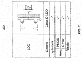
- FIG. 2 is a table 200 that describes the advantages of a Class-D LDO regulator, such as the Class-D LDO regulator 100, in accordance with an embodiment of the present disclosure.
- the table 200 summarizes the advantages (indicated by a check mark) of Class-D LDO regulators (such as Class-D LDO regulator 100).
- the diagram in the top row of the table represents simplified circuit diagrams of the Class-D LDO regulator.
- the shaded rectangle represents an effective signal swing at the gate of the final PMOS transistor (e.g., the power transistor).
- the Class-D LDO regulator 100 uses the full swing between VDD and VSS, having a range of VDD-VSS.
- the shaded region within the power transistor represents the concentration of the inverse carrier in the channel.
- the Class-D LDO regulator 100 is capable of carrying higher current density.
- Analog LDO regulators require large quiescent current and have large PMOS area (e.g., area of the power transistor).
- Digital LDO regulators have output ripple and large driver area.
- the Class-D LDO regulator described herein has low quiescent current, has small PMOS area and small driver area, and has low output ripple.
- the Class-D LDO regulator is accordingly efficient in power and area.
- FIG. 3 is a diagram of an example circuit implementation of a Class-D driven LDO regulator 300, in accordance with an embodiment of the present disclosure.
- the Class-D driven LDO regulator 300 includes an error amplifier 350, a PWM generator 352, and a power PMOS unit 354. Similar to the Class-D LDO regulator 100 described in relation to FIG. 1 , the error amplifier 350 compares a feedback signal Vfb to a reference voltage Vref, and provides the difference signal to the PWM generator 352. Moreover, the PWM generator 352 generates two PWM signals based on the difference signal from the error amplifier 350. The first PWM signal is an "UP" signal, and the second PWM signal is a "DN" signal. As is described in detail below, the UP and DN signals are both used to control the voltage of the gate of the last PMOS transistor, VG within the power PMOS unit 354.
- the UP signal is provided to the gate of a PMOS transistor within the power PMOS unit 354, and the DN signal is provided to the gate of an NMOS transistor within the power PMOS unit 354.
- the PMOS and NMOS transistors are connected in series at their drains, which provides input to the gate of a final PMOS transistor within the power PMOS unit 354.
- the final PMOS transistor provides the output voltage Vout.
- the feedback voltage Vfb is equal to or lower than the output voltage Vout, in some embodiments. In some embodiments, the feedback voltage Vfb is the same as the output voltage Vout. In other embodiments, a voltage divider is used to force Vfb to be a fixed fraction of Vout.
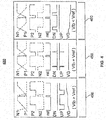
- FIG. 4 depicts time plots for three different states of the Class-D LDO regulator 300, in accordance with an embodiment of the present disclosure.
- the three states include: a first state 456 when Vfb is greater than Vref (left), a second state 458 when Vfb is equal to Vref (middle), and a third state 460 when Vfb is less than Vref (right).
- the Class-D controller e.g., the error amplifier 350 and the PWM generator 352 drives the power transistor gate (e.g., the power PMOS transistor 354, or more specifically, the rightmost PMOS transistor in the power PMOS transistor 354).
- the power transistor gate voltage (VG) takes on one of three states (high, low, or holding), based on the feedback voltage Vfb.
- the pulse widths of the UP and DN signals are modulated by the error voltage Vfb - Vref.
- the error amplifier 350 uses a transconductance stage to convert error voltage to output current.
- the tristate PWM generator 352 generates a reset pulse that sets the capacitor nodes P1 and N1 to VSS and VDD, respectively. These two nodes ramp up and down with a slope modulated by the output current of the error amplifier 350. The timing difference between P1 rising and N1 falling generates the differential PWM signals UP and DN.
- the sink current from the output of the error amplifier 350 slows the voltage amplitude rising at P1 and enables the voltage amplitude to quickly fall at N1. This generates a down pulse at UP, which pulls up the power transistor gate, VG.
- the source current from the output of the error amplifier 350 makes the voltage amplitude rising at P1 faster and the voltage amplitude falling at N1 slower. This generates an up pulse at DN, which pulls down the power transistor gate, VG.
- the Class-D LDO regulator circuit is configured to operate at low supply level, which makes it suitable for LDO applications.
- the Class-D LDO regulator consumes 152 ⁇ A current at 120 MHz PWM operation frequency.
- the circuit diagram in FIG. 3 and the corresponding timing diagrams in FIG. 4 depict one illustrative example of an implementation of a Class-D LDO regulator. In general, any number of different implementations of a Class-D LDO regulator are used that include an error amplifier, a PWM generator, and one or more transistors, without departing from the scope of the present disclosure.
- the Class-D driver Since the transistors in the driver stage (e.g., the transistors driven by UP and DN signals in the PWM generator 352) behave as complementary switches (meaning that they have interconnections such that when one is on, the other is off, and vice versa), the Class-D driver has much lower quiescent current than a typical analog Class-A or Class-AB driver. Moreover, rail-to-rail output range is a benefit of a Class-D driver (as it is in the digital LDO), and it helps to increase the output current density of the power transistor. For the analog LDO regulator, headroom is reserved to keep the transistors in a saturation mode. For example, an analog LDO regulator may have an effective output range in the analog driver that is VDD-2VDSAT. In this case, a minimal voltage VDSAT is reserved for both PMOS and NMOS transistors. Hence, the Class-D structure described herein is suitable for LDO regulation and low supply applications.
- Output ripple is an intrinsic problem in digital LDO regulators, due to the limited resolution of digitization.
- a digital LDO regulator activates a discrete number of power transistor units, each of which is configured to deliver a discrete amount of unit current, such that a switching ripple occurs when the load current is not an integer multiple of the unit current.
- the Class-D LDO regulator avoids output ripple that is inherent in a digital LDO regulator because of its finite resolution.
- the Class-D driver e.g., the PWM generator 352 outputs a tristate PWM signal (e.g., VG at the power PMOS 354).
- the power transistor gate VG senses digital pulses during transient response, but settles to an analog voltage level in the steady state. This behavior renders a Class-D LDO to be a ripple-less linear regulator.
- a low pass filter follows the Class-D driver, in an embodiment.
- LPF low pass filter
- the introduction of an LPF following the Class-D LDO regulator would add an extra pole into the feedback loop. This is generally undesirable because the extra pole would introduce stability problems.
- the circuit is redesigned to push the pole away from the loop bandwidth or to introduce a zero in the feedback loop. However, doing this would make the circuit complicated.
- the PMOS transistor 137 from FIG. 1 is implemented as a distributed LPF in a power-transistor gate resistance Rg and capacitance Cg, in accordance with embodiments as are described below in relation to FIGS. 5-10 .
- FIG. 5 is a circuit diagram 500 of a power transistor implemented as a distributed system, in accordance with an embodiment of the present disclosure.
- the transistor 562 in the left circuit diagram of FIG. 5 is implemented as a distributed system 564 in the right circuit diagram of FIG. 5 , in accordance with an embodiment of the disclosure.
- the distributed system 564 is referred to herein as a distributed-gate-resistance power transistor.
- the distributed system 564 includes an array of PMOS transistors. The drains of the PMOS transistors in the array of PMOS transistors are all connected to the same voltage Vout, and the sources of the PMOS transistors in the array of PMOS transistors are all connected to the same voltage VDD.
- the gates of the PMOS transistors in the array of PMOS transistors are connected to one another in series via resistors.
- the array of transistors in the distributed system 564 functions as a distributed RC network, whose transfer function is depicted in FIG. 8 .
- FIG. 6 depicts the LPF in a block diagram 700, in accordance with an embodiment of the present disclosure.
- the block diagram 600 depicts a tri-state PWM signal 670 that is provided to an LPF block 672, which low-pass filters the PWM signal 670 and provides the low-pass output to the gate of the PMOS transistor 674.
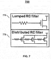
- FIG. 7 depicts the LPF in a circuit diagram 700, in accordance with an embodiment of the present disclosure.
- the circuit diagram 700 includes the diagram of a lumped RC filter 776 (with a simple resistor preceding the gate of a PMOS transistor) as well as the diagram of a distributed RC filter 778 (with an array of transistors connected to one another in the same manner as in the distributed system 564 in FIG. 5 ).
- the distributed RC filter 778 includes an array of PMOS transistors, where their drains are connected to the same voltage, their sources are connected to the same voltage, and their gates are connected to one another in series via resistors.
- FIG. 8 depicts plots of the transfer function 800 of the LPF, in accordance with an embodiment of the present disclosure.
- the transfer function 800 includes a plot of the amplitude (on top, in dB) and a plot of the phase (on bottom, in degrees), both as a function of frequency (in Hz).
- Different transfer functions are shown for the Class-D LDO regulator (1) without an LPF, (2) with a lumped RC LPF, and (3) with a distributed RC filter, as described above in relation to FIGS. 5-7 .
- the phase of the distributed RC filter has a relatively flat region between 1 MHz and 10 MHz, indicating that this bandwidth is an appropriate operating range for the Class-D LDO regulator.
- changing the characteristics of the Class-D LDO regulator such as the capacitor and resistors and other internal circuit characteristics, adjusts the location of the flat region and changes the optimal bandwidth for the Class-LDO regulator.
- FIG. 9 depicts a layout floor plan 980 and a circuit diagram 982 for the distributed-gate-resistance power transistor, in accordance with an embodiment of the present disclosure.
- the circuit diagram 982 includes an array of transistors that have the same drain voltages (Vout), the same source voltages (VDD), and gates that are connected in series via resistors, which are referred to herein as "gate resistors".
- Vout drain voltages
- VDD source voltages
- gate resistors the array of transistors that are connected in series via resistors.
- the array of transistors are connected by gate resistors. Accordingly, the entire power transistor array is interpreted as a distributed RC network, in an embodiment.
- the gate resistors are implemented as physical resistors connecting the gates of the transistors in the array in series. In other embodiments, no physical resistors are used, and the gate resistors are implemented by using a resistive or partially resistive material to form the gates of the transistors in the array.
- the gates are formed from a polycrystalline silicon material, which have some resistance to form built-in gate resistors. Forming the gate resistors through the inherent characteristics of the gate material is be desirable to increase area efficiency, in an embodiment.
- the layout floor plan 980 depicts the layout of an implementation of the circuit diagram 982, where no physical resistors are used, and the gate resistors are implemented by using a polycrystalline silicon material for the gates.
- the layout floor plan 980 includes an input gate voltage VG_IN metal region and an output gate voltage VG OUT metal region.
- Two parallel polycrystalline silicon gate (“poly gate”) lines extend from the VG_IN metal region across a set of diffusion regions, and terminate at a bottom metal portion.
- Two more parallel poly gate lines extend from the bottom metal portion across the set of diffusion regions and terminate at the VG_OUT metal region.
- the layout floor plan 980 depicts an implementation in which the inherent resistance of poly gate material is used to provide resistance between the gates of the PMOS transistors in the circuit diagram 982.
- FIG. 10 includes two such examples.
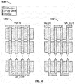
- FIG. 10 depicts two layout floor plans 1090 and 1092 for the distributed-gate-resistance power transistor, in accordance with an embodiment of the present disclosure.
- the layout floor plans 1090 and 1092 are similar to the layout floor plan 980, except that the poly gates are connected in parallel (1090) or in series (1092).
- the layout floor plan 1090 includes a VG_IN metal region, a VG_OUT metal region, and four parallel poly gate lines extending from VG_IN to VG_OUT.
- the layout floor plan 1092 includes a VG_IN metal region, a VG_OUT metal region, three intermediate metal regions, and a single poly gate line that snakes across the metal regions and terminates at VG_IN and VG_OUT.
- FIG. 11 depicts a table 1100 that summarizes the performance of an example Class-D LDO regulator as described herein, in accordance with an embodiment of the present disclosure.
- a Class-D LDO regulator is fabricated in a 28 nm CMOS process.
- the input voltage ranges from 1.8 V to 1.2 V, and has an output voltage of 1.05V with 1 A load capacity.
- the power transistor in this work uses a 1.8 V PMOS with width 40 mm and length 0.18 ⁇ m.
- the sheet resistance of the salicide gate in the 28 nm CMOS process is about 30 ⁇ /sq.
- Rg is configurable by series or parallel connection of the transistor gates. In an example, Rg is selected to be 23 k ⁇ , to achieve fast transient response as well as robust stability.
- the LDO loop bandwidth is 2.5 MHz at full load, which is far below the PWM switching frequency. Without extra compensation, the LDO loop has worst-case 40 degree phase margin and 46 dB gain margin across corners and loads.
- the power transistor e.g., the PMOS transistor 137 or the power transistor 354
- the Class-D controller e.g., the error amplifier 350 and the PWM generator 352
- a minimum 1 ⁇ F external capacitor is used for stability.
- the Class-D LDO regulator delivers 1 A of load current (Imax) while consuming about 152 ⁇ A quiescent current (Iq). In steady state, the measured output has no visible ripple, which is as good as a linear regulator.
- a power analyzer is used for a load test, in an embodiment.
- the transient overshoot and undershoot voltages are around 90 mV and 20 mV for a load step of 1000 mA/0.5 ⁇ s with supply at 1.35 V.
- Typical load regulation is 15 mV/A.
- the Class-D LDO regulator has line regulation of 1 mV when the supply is swept from 1.8 V to 1.2 V.
- Analog LDO regulators have linear output but large quiescent current when the power transistor scales up.
- Digital LDO regulators have smaller quiescent current, but the control logic complexity and area scales with the power-transistor units.
- the Class-D LDO regulator such as the Class-D LDO regulator 100 described in relation to FIG. 1 , avoids the disadvantages of both analog and digital LDO regulators by producing linear output with small quiescent current.
- the Class-D LDO regulator as described herein readily supports power transistor scaling and process migration, in some embodiments.
- the timing efficiency which is represented in FIG. 11 by a timing figure of merit (FOMT T ) is an evaluation of how fast of a response can the LDO regulator achieve, with a normalized power and capacitor parameter.
- the controller area efficiency which is represented in FIG. 11 by an area figure of merit (FOM A ), is the area of the controller (in mm 2 ) divided by the maximum load (in A), and is an area and current-efficient solution for high current capacity LDO applications.
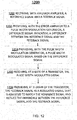
- FIG. 12 shows a high level flow chart for a process 1200 for using a Class-D LDO regulator to regulate an output voltage to match a reference voltage, in accordance with an embodiment of the present disclosure.
- the process 1200 includes receiving, with an error amplifier, a reference signal and a feedback signal (1202), and providing, with the error amplifier to a PWM generator, a difference signal indicating a voltage difference between the reference signal and the feedback signal (1204).
- the feedback signal is the same as Vout, in an embodiment, or is a fixed fraction of Vout, in an embodiment.
- the process 1200 further includes providing, with the PWM generator, a pulse width modulated signal based on the difference signal (1204), receiving, at a gate of one or more transistors, the pulse width modulated signal (1206), and providing, at a drain of the one or more transistors, the feedback signal as a regulated voltage that is adjusted to match the reference signal so as to reduce the voltage difference between the reference signal and the feedback signal (1208).
- an error amplifier receives a reference signal and a feedback signal.
- the reference signal corresponds to a desired voltage level or amplitude that the Class-D LDO regulator is configured to provide.
- the feedback signal corresponds to an output signal provided by a transistor within the Class-D LDO regulator (e.g., Vout or a fixed fraction of Vout).
- the error amplifier provides a difference signal to a PWM generator (such as the PWM generator 134 or 352, for example).
- the difference signal indicates a voltage difference between an amplitude of the reference signal and an amplitude of the feedback signal.
- the PWM generator provides a pulse width modulated signal based on the difference signal.
- the PWM generator provides two pulse width modulated signals: a first pulse width modulated signal corresponds to an UP signal, and a second pulse width modulated signal corresponds to a DN signal (such as the UP and DN signals described in relation to FIGS. 3 and 4 ).
- a first pulse width modulated signal corresponds to an UP signal
- a second pulse width modulated signal corresponds to a DN signal (such as the UP and DN signals described in relation to FIGS. 3 and 4 ).
- a first pulse width modulated signal corresponds to an UP signal
- a second pulse width modulated signal corresponds to a DN signal (such as the UP and DN signals described in relation to FIGS. 3 and 4 ).
- a second pulse width modulated signal corresponds to a DN signal (such as the UP and DN signals described in relation to FIGS. 3 and 4 ).
- the widths of the pulses define time interval
- the gate of one or more transistors receives the pulse width modulated signal.
- a first PMOS transistor receives the UP signal at its gate while an NMOS transistor receives the DN signal at its gate, in an embodiment.
- the first PMOS transistor and the NMOS transistor share a drain node that is also connected to the gate of a second PMOS transistor, such as that shown in 354 of FIG. 3 .
- the states of these three transistors are determined based on the pulse width modulated signals that are received at their respective gates, which is described in detail below.
- the DN signal is maintained without change, while the UP signal includes pulses whose widths define time intervals during which increased current passes through the first PMOS transistor, causing the drain voltage of the first PMOS transistor (and accordingly the gate voltage of the second PMOS transistor) to increase.
- the increase in the gate voltage of the second PMOS transistor causes the amount of current passing through the second PMOS transistor to decrease, thereby decreasing the feedback signal, or the drain voltage of the second PMOS transistor.
- the UP signal when the reference signal exceeds the feedback signal, the UP signal is maintained without change, while the DN signal includes pulses whose widths define time intervals during which decreased current passes through the NMOS transistor, causing the drain voltage of the NMOS transistor (and accordingly the gate voltage of the second PMOS transistor) to decrease. This causes the amount of current passing through the second PMOS transistor to increase, thereby increasing the feedback signal, or the drain voltage of the second PMOS transistor.
- the DN and UP signals are complementary (e.g., the DN signal is high when the UP signal is low, and the DN signal is low when the UP signal is high). In this case, the UP and DN signals cancel one another out, and the gate voltage of the second PMOS transistor is maintained without change to maintain the amplitude of the feedback signal.
- the one or more transistors are implemented as a distributed array of transistors, such as that depicted in FIGS. 5 , 9 , or 10 .
- the array of transistors is suitably arranged to have the same source node and the same drain node, with gate nodes connected in series, separated by resistors.
- the material used to form the gates of the transistors include a polycrystalline silicon material that has inherent resistive characteristics. These characteristics further form a distributed RC filter in an embodiment, such as that described with reference to FIG. 7 , that low pass filters the pulse width modulated signal and suppresses switching ripple.
- the drain of the one or more transistors provides the feedback signal as a regulated voltage that is adjusted to match the reference signal so as to reduce the voltage difference between the reference signal and the feedback signal.
Landscapes
- Engineering & Computer Science (AREA)
- Physics & Mathematics (AREA)
- Electromagnetism (AREA)
- General Physics & Mathematics (AREA)
- Radar, Positioning & Navigation (AREA)
- Automation & Control Theory (AREA)
- Continuous-Control Power Sources That Use Transistors (AREA)
- Amplifiers (AREA)
Applications Claiming Priority (1)
| Application Number | Priority Date | Filing Date | Title |
|---|---|---|---|
| US201662393396P | 2016-09-12 | 2016-09-12 |
Publications (2)
| Publication Number | Publication Date |
|---|---|
| EP3306433A2 true EP3306433A2 (de) | 2018-04-11 |
| EP3306433A3 EP3306433A3 (de) | 2018-05-02 |
Family
ID=59677146
Family Applications (1)
| Application Number | Title | Priority Date | Filing Date |
|---|---|---|---|
| EP17187098.3A Withdrawn EP3306433A3 (de) | 2016-09-12 | 2017-08-21 | Klasse-d-angetriebener ldo-regler |
Country Status (2)
| Country | Link |
|---|---|
| US (1) | US10126769B2 (de) |
| EP (1) | EP3306433A3 (de) |
Families Citing this family (4)
| Publication number | Priority date | Publication date | Assignee | Title |
|---|---|---|---|---|
| US11906997B2 (en) | 2021-05-14 | 2024-02-20 | Taiwan Semiconductor Manufacturing Company, Ltd. | Low-dropout (LDO) voltage regulator including amplifier and decoupling capacitor |
| EP4198676A1 (de) | 2021-12-17 | 2023-06-21 | Nxp B.V. | Spannungsregelung unter verwendung eines delta-sigma-modulators, vorrichtung und verfahren |
| US12326748B2 (en) | 2022-02-10 | 2025-06-10 | Nxp B.V. | Linear voltage regulator using serial bit stream for voltage regulation |
| CN118226913A (zh) * | 2022-12-21 | 2024-06-21 | 川能电子有限公司 | 双回路线性稳压器及其稳定度补偿电路与控制方法 |
Citations (3)
| Publication number | Priority date | Publication date | Assignee | Title |
|---|---|---|---|---|
| US20110018508A1 (en) * | 2007-10-12 | 2011-01-27 | Paul Ueunten | Method and apparatus for high performance switch mode voltage regulators |
| US20140084886A1 (en) * | 2012-09-27 | 2014-03-27 | Olivier Causse | Converter and method |
| US9729058B2 (en) * | 2015-09-22 | 2017-08-08 | Stmicroelectronics S.R.L. | Converter circuit with injection of ripple current for comparison |
Family Cites Families (30)
| Publication number | Priority date | Publication date | Assignee | Title |
|---|---|---|---|---|
| US5838271A (en) * | 1997-01-31 | 1998-11-17 | Lg Semicon Co., Ltd. | Digital to analog converter and bias circuit therefor for providing weighed currents |
| US6150803A (en) * | 2000-03-28 | 2000-11-21 | Linear Technology Corporation | Dual input, single output power supply |
| US6551941B2 (en) * | 2001-02-22 | 2003-04-22 | Applied Materials, Inc. | Method of forming a notched silicon-containing gate structure |
| US7737666B2 (en) * | 2003-08-04 | 2010-06-15 | Marvell World Trade Ltd. | Split gate drive scheme to improve reliable voltage operation range |
| CN100399689C (zh) * | 2004-04-27 | 2008-07-02 | 株式会社理光 | 开关调整器以及开关调整器的输出电压切换方法 |
| US6969977B1 (en) * | 2004-06-10 | 2005-11-29 | National Semiconductor Corporation | Soft-start voltage regulator circuit |
| JP4463635B2 (ja) * | 2004-07-20 | 2010-05-19 | 株式会社リコー | スイッチングレギュレータ、スイッチングレギュレータを使用した電源回路及びスイッチングレギュレータを使用した二次電池の充電回路 |
| TWI277850B (en) * | 2004-08-27 | 2007-04-01 | Richtek Techohnology Corp | A spring type modulation circuit and method for voltage regulator |
| TWI307203B (en) * | 2005-06-03 | 2009-03-01 | Richtek Technology Corp | A pulse width modulation system with nonlinear ramp |
| WO2007024675A1 (en) * | 2005-08-23 | 2007-03-01 | Analog Devices, Inc. | Improving transient behavior while switching between control loops in a switching voltage regulator |
| US7436158B2 (en) * | 2006-07-27 | 2008-10-14 | Richtek Technology Corp. | Low-gain current-mode voltage regulator |
| KR100804643B1 (ko) | 2006-11-30 | 2008-02-20 | 삼성전자주식회사 | 전압 레귤레이터, 이를 포함하는 디지털 앰프 및 전압 조절방법 |
| US7982445B1 (en) * | 2007-11-08 | 2011-07-19 | National Semiconductor Corporation | System and method for controlling overshoot and undershoot in a switching regulator |
| US7834601B2 (en) * | 2007-11-09 | 2010-11-16 | Freescale Semiconductor, Inc. | Circuit and method for reducing output noise of regulator |
| JP4618339B2 (ja) * | 2008-06-20 | 2011-01-26 | ミツミ電機株式会社 | Dc−dcコンバータ |
| US8269474B2 (en) * | 2008-07-23 | 2012-09-18 | Intersil Americas Inc | System and method for reducing voltage overshoot during load release within a buck regulator |
| US8148967B2 (en) * | 2008-08-05 | 2012-04-03 | Intersil Americas Inc. | PWM clock generation system and method to improve transient response of a voltage regulator |
| TWI420796B (zh) * | 2009-02-27 | 2013-12-21 | Asus Technology Pte Ltd | 直流轉直流變換器及其減小過衝現象的控制方法 |
| IT1394910B1 (it) * | 2009-06-10 | 2012-07-20 | St Microelectronics Srl | Metodo e relativo anello di controllo in retroazione di un convertitore di tensione |
| US8395367B2 (en) * | 2009-08-05 | 2013-03-12 | Upi Semiconductor Corporation | DC-DC converter with a constant on-time pulse width modulation controller |
| JP2011061989A (ja) * | 2009-09-10 | 2011-03-24 | Renesas Electronics Corp | スイッチングレギュレータ |
| JP5481161B2 (ja) * | 2009-10-30 | 2014-04-23 | ルネサスエレクトロニクス株式会社 | 半導体装置および電源装置 |
| EP2365622B1 (de) * | 2010-03-08 | 2017-05-10 | Nxp B.V. | Schaltung und Verfahren zur Steuerung eines Schaltnetzteiles mit schnellem transientem Ansprechverhalten |
| US8841893B2 (en) | 2010-12-16 | 2014-09-23 | International Business Machines Corporation | Dual-loop voltage regulator architecture with high DC accuracy and fast response time |
| CN102243505B (zh) | 2011-07-07 | 2013-08-14 | 矽力杰半导体技术(杭州)有限公司 | 一种低失调、快速响应的电压控制电流源、控制方法以及应用其的电源电路 |
| CN102931842A (zh) * | 2012-10-12 | 2013-02-13 | 华为技术有限公司 | 芯片动态调压电路和终端设备 |
| TWI495236B (zh) * | 2012-12-21 | 2015-08-01 | System General Corp | 控制電路及控制方法 |
| WO2014187965A1 (en) * | 2013-05-24 | 2014-11-27 | Zentrum Mikroelektronik Dresden Ag | Pwm calculation after light load to high load transition |
| KR101540858B1 (ko) | 2013-12-13 | 2015-07-30 | 강원대학교산학협력단 | Sdm을 이용한 디지털 제어 방식의 ldo 레귤레이터 |
| US9450492B1 (en) * | 2015-06-24 | 2016-09-20 | Infineon Technologies Ag | System and method for controlling a duty cycle of a switched-mode power supply |
-
2017
- 2017-07-31 US US15/664,708 patent/US10126769B2/en active Active
- 2017-08-21 EP EP17187098.3A patent/EP3306433A3/de not_active Withdrawn
Patent Citations (3)
| Publication number | Priority date | Publication date | Assignee | Title |
|---|---|---|---|---|
| US20110018508A1 (en) * | 2007-10-12 | 2011-01-27 | Paul Ueunten | Method and apparatus for high performance switch mode voltage regulators |
| US20140084886A1 (en) * | 2012-09-27 | 2014-03-27 | Olivier Causse | Converter and method |
| US9729058B2 (en) * | 2015-09-22 | 2017-08-08 | Stmicroelectronics S.R.L. | Converter circuit with injection of ripple current for comparison |
Also Published As
| Publication number | Publication date |
|---|---|
| US10126769B2 (en) | 2018-11-13 |
| EP3306433A3 (de) | 2018-05-02 |
| US20180074536A1 (en) | 2018-03-15 |
Similar Documents
| Publication | Publication Date | Title |
|---|---|---|
| EP1569062B1 (de) | Effiziente Frequenzkompensation für lineare Spannungsregler. | |
| US8624568B2 (en) | Low noise voltage regulator and method with fast settling and low-power consumption | |
| US7323853B2 (en) | Low drop-out voltage regulator with common-mode feedback | |
| EP1378808B1 (de) | Regelungseinrichtung mit kleiner Verlustspannung, mit grossem Lastbereich und schneller innerer Regelschleife | |
| US9122293B2 (en) | Method and apparatus for LDO and distributed LDO transient response accelerator | |
| CN112578842B (zh) | 具有改进的电源抑制的低压差电压调节器 | |
| EP2846213B1 (de) | Verfahren und Vorrichtung zur Begrenzung des Einschaltstroms bei Inbetriebnahme für Regler mit geringem Spannungsabfall | |
| US7893671B2 (en) | Regulator with improved load regulation | |
| US7218083B2 (en) | Low drop-out voltage regulator with enhanced frequency compensation | |
| US6703816B2 (en) | Composite loop compensation for low drop-out regulator | |
| US10126769B2 (en) | Class-D driven low-drop-output (LDO) regulator | |
| US10193449B2 (en) | Buck voltage converter | |
| US9874887B2 (en) | Voltage regulator with adjustable feedback | |
| US20120262135A1 (en) | LDO with improved stability | |
| US9110488B2 (en) | Wide-bandwidth linear regulator | |
| US7719241B2 (en) | AC-coupled equivalent series resistance | |
| US11009900B2 (en) | Method and circuitry for compensating low dropout regulators | |
| US9831757B2 (en) | Voltage regulator | |
| CN115097894A (zh) | 一种高电源抑制比的无片外电容的推拉型ldo | |
| US20170364111A1 (en) | Linear voltage regulator | |
| US10558232B2 (en) | Regulator circuit and control method | |
| EP3250977B1 (de) | Kapazitativ gekoppelte hybride parallele stromversorgung | |
| Xu et al. | 5.10 A 1A LDO regulator driven by a 0.0013 mm 2 class-D controller | |
| US7564299B2 (en) | Voltage regulator | |
| US20250123646A1 (en) | Low dropout (ldo) regulator |
Legal Events
| Date | Code | Title | Description |
|---|---|---|---|
| PUAI | Public reference made under article 153(3) epc to a published international application that has entered the european phase |
Free format text: ORIGINAL CODE: 0009012 |
|
| STAA | Information on the status of an ep patent application or granted ep patent |
Free format text: STATUS: THE APPLICATION HAS BEEN PUBLISHED |
|
| PUAL | Search report despatched |
Free format text: ORIGINAL CODE: 0009013 |
|
| AK | Designated contracting states |
Kind code of ref document: A2 Designated state(s): AL AT BE BG CH CY CZ DE DK EE ES FI FR GB GR HR HU IE IS IT LI LT LU LV MC MK MT NL NO PL PT RO RS SE SI SK SM TR |
|
| AX | Request for extension of the european patent |
Extension state: BA ME |
|
| AK | Designated contracting states |
Kind code of ref document: A3 Designated state(s): AL AT BE BG CH CY CZ DE DK EE ES FI FR GB GR HR HU IE IS IT LI LT LU LV MC MK MT NL NO PL PT RO RS SE SI SK SM TR |
|
| AX | Request for extension of the european patent |
Extension state: BA ME |
|
| RIC1 | Information provided on ipc code assigned before grant |
Ipc: G05F 1/575 20060101ALI20180329BHEP Ipc: G05F 1/56 20060101AFI20180329BHEP |
|
| STAA | Information on the status of an ep patent application or granted ep patent |
Free format text: STATUS: REQUEST FOR EXAMINATION WAS MADE |
|
| 17P | Request for examination filed |
Effective date: 20181031 |
|
| RBV | Designated contracting states (corrected) |
Designated state(s): AL AT BE BG CH CY CZ DE DK EE ES FI FR GB GR HR HU IE IS IT LI LT LU LV MC MK MT NL NO PL PT RO RS SE SI SK SM TR |
|
| RAP1 | Party data changed (applicant data changed or rights of an application transferred) |
Owner name: MARVELL ASIA PTE, LTD. |
|
| STAA | Information on the status of an ep patent application or granted ep patent |
Free format text: STATUS: EXAMINATION IS IN PROGRESS |
|
| 17Q | First examination report despatched |
Effective date: 20200807 |
|
| STAA | Information on the status of an ep patent application or granted ep patent |
Free format text: STATUS: THE APPLICATION IS DEEMED TO BE WITHDRAWN |
|
| 18D | Application deemed to be withdrawn |
Effective date: 20220301 |