EP3306363A1 - Method for producing phosphor plate - Google Patents
Method for producing phosphor plate Download PDFInfo
- Publication number
- EP3306363A1 EP3306363A1 EP16803181.3A EP16803181A EP3306363A1 EP 3306363 A1 EP3306363 A1 EP 3306363A1 EP 16803181 A EP16803181 A EP 16803181A EP 3306363 A1 EP3306363 A1 EP 3306363A1
- Authority
- EP
- European Patent Office
- Prior art keywords
- phosphor
- sheet
- greensheet
- ceramic plate
- face
- Prior art date
- Legal status (The legal status is an assumption and is not a legal conclusion. Google has not performed a legal analysis and makes no representation as to the accuracy of the status listed.)
- Withdrawn
Links
Images



Classifications
-
- H—ELECTRICITY
- H10—SEMICONDUCTOR DEVICES; ELECTRIC SOLID-STATE DEVICES NOT OTHERWISE PROVIDED FOR
- H10H—INORGANIC LIGHT-EMITTING SEMICONDUCTOR DEVICES HAVING POTENTIAL BARRIERS
- H10H20/00—Individual inorganic light-emitting semiconductor devices having potential barriers, e.g. light-emitting diodes [LED]
- H10H20/80—Constructional details
- H10H20/85—Packages
- H10H20/851—Wavelength conversion means
- H10H20/8511—Wavelength conversion means characterised by their material, e.g. binder
- H10H20/8512—Wavelength conversion materials
-
- H—ELECTRICITY
- H10—SEMICONDUCTOR DEVICES; ELECTRIC SOLID-STATE DEVICES NOT OTHERWISE PROVIDED FOR
- H10H—INORGANIC LIGHT-EMITTING SEMICONDUCTOR DEVICES HAVING POTENTIAL BARRIERS
- H10H20/00—Individual inorganic light-emitting semiconductor devices having potential barriers, e.g. light-emitting diodes [LED]
- H10H20/01—Manufacture or treatment
-
- B—PERFORMING OPERATIONS; TRANSPORTING
- B28—WORKING CEMENT, CLAY, OR STONE
- B28B—SHAPING CLAY OR OTHER CERAMIC COMPOSITIONS; SHAPING SLAG; SHAPING MIXTURES CONTAINING CEMENTITIOUS MATERIAL, e.g. PLASTER
- B28B11/00—Apparatus or processes for treating or working the shaped or preshaped articles
- B28B11/14—Apparatus or processes for treating or working the shaped or preshaped articles for dividing shaped articles by cutting
-
- C—CHEMISTRY; METALLURGY
- C09—DYES; PAINTS; POLISHES; NATURAL RESINS; ADHESIVES; COMPOSITIONS NOT OTHERWISE PROVIDED FOR; APPLICATIONS OF MATERIALS NOT OTHERWISE PROVIDED FOR
- C09K—MATERIALS FOR MISCELLANEOUS APPLICATIONS, NOT PROVIDED FOR ELSEWHERE
- C09K11/00—Luminescent materials, e.g. electroluminescent or chemiluminescent
- C09K11/02—Use of particular materials as binders, particle coatings or suspension media therefor
-
- H—ELECTRICITY
- H10—SEMICONDUCTOR DEVICES; ELECTRIC SOLID-STATE DEVICES NOT OTHERWISE PROVIDED FOR
- H10H—INORGANIC LIGHT-EMITTING SEMICONDUCTOR DEVICES HAVING POTENTIAL BARRIERS
- H10H20/00—Individual inorganic light-emitting semiconductor devices having potential barriers, e.g. light-emitting diodes [LED]
- H10H20/01—Manufacture or treatment
- H10H20/036—Manufacture or treatment of packages
- H10H20/0361—Manufacture or treatment of packages of wavelength conversion means
-
- H—ELECTRICITY
- H10—SEMICONDUCTOR DEVICES; ELECTRIC SOLID-STATE DEVICES NOT OTHERWISE PROVIDED FOR
- H10H—INORGANIC LIGHT-EMITTING SEMICONDUCTOR DEVICES HAVING POTENTIAL BARRIERS
- H10H20/00—Individual inorganic light-emitting semiconductor devices having potential barriers, e.g. light-emitting diodes [LED]
- H10H20/80—Constructional details
- H10H20/85—Packages
- H10H20/851—Wavelength conversion means
- H10H20/8514—Wavelength conversion means characterised by their shape, e.g. plate or foil
Definitions
- the present invention relates to a method for producing a phosphor plate, in particular, to a phosphor plate suitably used for an optical semiconductor device.
- a luminescence conversion element including a ceramic material is used for an optoelectronic component along with a radiation-emitting semiconductor chip.
- the luminescence conversion element is formed, for example, into a letter L shape plate having a cut portion (e.g., see Patent Document 1).
- Patent Document 1 has proposed an optoelectronic component in which the lower face of the luminescence conversion element is joined to the upper face of the radiation-emitting semiconductor chip, and the bonding pad provided in the corner region of the radiation-emitting semiconductor chip exposed from the cut portion is connected by a bonding wire.
- Patent Document 1 has also proposed the following method as the method for producing a luminescence conversion element. That is, first, on the support, a partial shaped bodies composed of the luminescence conversion material is molded into a bar having a rectangular cross section and extending into front-back directions, then, the upper right corner portion viewed in cross section of the partial shaped bodies is ground along with front-back directions, and thereafter, the partial shaped bodies is cut along the orthogonal direction (up-down left-right directions) relative to front-back directions.
- Patent Document 1 Japanese Unexamined Patent Application Publication (Translation of PCT Application) 2014-502368
- An object of the present invention is to provide a method for producing a phosphor plate that is easy and excellent in production efficiency.
- the through holes can be easily formed, and the phosphor plate can be produced with excellent production efficiency.
- FIG. 1A to FIG. 1G An embodiment of the method for producing a phosphor plate of the present invention and the method for producing an optical semiconductor device are described with reference to FIG. 1A to FIG. 1G .
- directions are in conformity with direction arrows.
- a method for producing a phosphor plate includes, in sequence, a step (1) (ref: FIG. 1A ), in which a phosphor sheet of the present invention is prepared as a greensheet 1; a step (2) (ref: FIG. 1B ), in which through holes 2 and penetration faces 3 fronting the through hole 2 are formed in the greensheet 1; a step (4) (ref: FIG. 1C ), in which a phosphor plate of the present invention is formed as a ceramic plate 4 produced by calcining the greensheet 1; a step (3) (ref: FIG. 1D and FIG. 1E ), in which the ceramic plate 4 is cut to form the plurality of phosphor plates 15 including the penetration faces 3; and a step (6) (ref: FIG. 1F ), in which the phosphor plate 15 is transferred from the supporting sheet 5 to the transfer sheet 20.
- step (1) (ref: FIG. 1A ), step (2) (ref: FIG. 1B ), step (4) (ref: FIG. 1C ), step (3) (ref: FIG. 1D and FIG. 1E ), and step (6) (ref: FIG. 1F ) are carried out sequentially.
- step (2) (ref: FIG. 1B )
- step (4) (ref: FIG. 1C )
- step (3) (ref: FIG. 1D and FIG. 1E )
- step (6) (ref: FIG. 1F ) are carried out sequentially.
- Each of the steps is described below.
- a greensheet 1 is prepared.
- the greensheet 1 can be prepared by a method such as, slurry (slip) molding; compression molding such as cold isostatic pressing (CIP) and hot isostatic pressing (HIP); and injection molding.
- slurry molding and compression molding are used, more preferably, slurry molding is used.
- slurry molding first, for example, a slurry containing a phosphor composition containing a phosphor material, organic particles, and a binder; and a dispersion medium is prepared.
- the phosphor material is a raw material composing phosphor, and is suitably selected in accordance with the phosphor.
- the phosphor has a function of converting wavelength, and examples thereof include yellow phosphor that can convert blue light to yellow light, and red phosphor that can convert blue light to red light.
- yellow phosphor examples include silicate phosphor such as (Ba,Sr,Ca) 2 SiO 4 ;Eu and (Sr,Ba) 2 SiO 4 :Eu (barium orthosilicate (BOS)); garnet phosphor having a garnet crystal structure such as (Y,Gd,Ba,Ca,Lu) 3 (Al,Si,Ge,B,P,Ga) 5 O 12 :Ce (YAG (yttrium • aluminum • garnet):Ce) and Tb 3 Al 3 O 12 : Ce (TAG (terbium • aluminum • gamet):Ce); and oxynitride phosphor such as Ca- ⁇ -SiAlON.
- silicate phosphor such as (Ba,Sr,Ca) 2 SiO 4 ;Eu and (Sr,Ba) 2 SiO 4 :Eu (barium orthosilicate (BOS)
- garnet phosphor having a garnet crystal structure such as (Y,
- red phosphor examples include nitride phosphors such as CaAlSiN 3 :Eu and CaSiN 2 :Eu.
- nitride phosphors such as CaAlSiN 3 :Eu and CaSiN 2 :Eu.
- garnet phosphor more preferably YAG:Ce (Y 3 Al 5 O 12 :Ce) is used.
- Examples of the phosphor material include a metal itself that composes phosphor, a metal oxide thereof, and a metal nitride.
- examples of the phosphor material include, when YAG: Ce is formed as the phosphor, metal oxides such as a yttrium-containing compound including yttrium oxide, an aluminum-containing compound including aluminum oxide, and a cerium-containing compound including cerium oxide are used.
- the phosphor material is formed, for example, into particles (or powder).
- the phosphor material has a purity of, for example, 99.0 mass% or more, preferably 99.9 mass% or more.
- the organic particles are contained in the phosphor composition as necessary to form micropores (not shown) in the ceramic plate 4.
- those materials that are thermally decomposed completely in the step (4) (described later) are used, and thermoplastic resin such as acrylic resin (to be specific, polymethyl methacrylate), styrene resin, acryl-styrene resin, polycarbonate resin, benzoguanamine resin, polyolefin resin, polyester resin, polyamide resin, and polyimide resin; and thermosetting resin such as epoxy resin and silicone resin are used.
- thermoplastic resin more preferably, acrylic resin is used.
- the average particle size of the organic particles is not particularly limited, and for example, it is 3.4 ⁇ m or more, preferably 4.0 ⁇ m or more, and for example, 25.0 ⁇ m or less, preferably 20.0 ⁇ m or less, more preferably 8.0 ⁇ m or less.
- the organic particle content relative to a total of the phosphor material content and the organic particles content is, for example, 1.5% by volume or more, preferably 2.0% by volume or more, and for example, 12.0% by volume or less, preferably 10.0% by volume or less, more preferably 8.0% by volume or less.
- binder examples include resin such as acrylic polymer, butyral polymer, vinyl polymer, and urethane polymer.
- examples of the binder also include water-soluble binders.
- acrylic polymer more preferably, water-soluble acrylic polymer is used.
- the binder content is set so that relative to 100 parts by volume of a total of the phosphor material and the binder, the binder content is, for example, 10 parts by volume or more, preferably 20 parts by volume or more, more preferably 30 parts by volume or more, and for example, 60 parts by volume or less, preferably 50 parts by volume or less, more preferably 40 parts by volume or less.
- the phosphor composition can further contain, for example, as necessary, additives such as a dispersing agent, a plasticizer, and a calcination auxiliary agent.
- additives such as a dispersing agent, a plasticizer, and a calcination auxiliary agent.
- the dispersion medium is not particularly limited, as long as it can disperse the phosphor material and the organic particles.
- examples of the dispersion medium include water, and an organic dispersion medium such as acetone, methyl ethyl ketone, methanol, ethanol, toluene, methyl propionate, and methyl cellosolve.
- water is used.
- the dispersion medium content relative to the slurry is, for example, 1 mass% or more, for example, 30 mass% or less.
- the above-described component is blended at the above-described ratio, and the mixture is subjected to, for example, wet blending with a ball mill.
- the above-described component can be subjected to wet blending all at once.
- the components other than the organic particles can be subjected to wet blending to prepare a first slurry, and then, the first slurry can be blended with organic particles by wet blending to prepare a slurry.
- the slurry is applied on the surface of the release sheet 10, and thereafter, dried.
- the release sheet 10 is formed from a flexible material.
- a polyester sheet such as polyethylene terephthalate (PET) sheet; a polycarbonate sheet; polyolefin sheets such as a polyethylene sheet and a polypropylene sheet; a polystyrene sheet; an acryl sheet; and resin sheets such as a silicone resin sheet and a fluorine resin sheet.
- foil of metals such as copper foil and stainless steel foil are used.
- a resin sheet even more preferably, a polyester sheet is used.
- the surface of the release sheet 10 may be treated for release in order to improve releasability, as necessary.
- the thickness of the release sheet 10 is set suitably in view of handleability and costs, and is, to be specific, 10 ⁇ m or more and 200 ⁇ m or less.
- the slurry is applied on the release sheet 10 by coating methods such as doctor blade coating, gravure coating, fountain coating, cast coating, spin coating, and roll coating.
- the drying temperature is, for example, 20°C or more, preferably 50°C or more, and for example, 200°C or less, preferably 150°C or less.
- the drying time is, for example, 1 minute or more, preferably 2 minutes or more, and for example, 24 hours or less, preferably 5 hours or less.
- the greensheet 1 is a sheet before calcining the ceramic plate 4 (ref: FIG. 1C ), and is a plate extending in front-back directions and left-right directions.
- a plurality of (a plurality of layers of) greensheets 1 can be laminated by heat lamination to obtain a greensheet laminate 1.
- the greensheet 1 (or greensheet laminate 1) has a thickness T1 of, for example, 10 ⁇ m or more, preferably 30 ⁇ m or more, and for example, 500 ⁇ m or less, preferably 200 ⁇ m or less.
- the plurality of through holes 2 are arranged in line in front-back directions and left-right directions in spaced-apart relation to each other (2 rows in front-back directions and 2 rows in left-right directions).
- the plurality of through holes 2 are round holes that penetrates the greensheet 1 in the thickness direction (up-down direction).
- the step (2) can be conducted by methods of making holes such as the following: for example, the greensheet 1 can be subjected to punching, blast processing, drilling, or laser processing with, for example, YAG laser.
- blast processing for example, direct pressure blast processing and siphon processing can be used.
- a resist is placed so as to cover the portions excluding the portions where through holes 2 are made, and then a blasting material is greensheet 1 is applied.
- the size of the through hole 2 is suitably adjusted by suitably adjusting the types and particle size of the blasting material used for blast processing, and the speed of blasting, or type (direct pressure ,siphon).
- Blast processing is preferable in view of productivity, compared with laser processing.
- the greensheet 1 is punched or the greensheet 1 is drilled.
- the greensheet 1 When the greensheet 1 is subjected to drilling, since a drill has a small diameter and easily damaged (broken), and therefore to prevent such problems, drilling process takes long time. Therefore, in view of shortening the takt time, more preferably, the greensheet 1 is punched.
- the penetration face 3 are inner periphery of the through hole 2 extending in the thickness direction (up-down direction) in the greensheet 1.
- the size of the through hole 2 and the penetration face 3 is suitably set in accordance with the size of the connection portion 25 and the wire 29 (ref: FIG. 1G ) of the optical semiconductor device 30 described later.
- the through hole 2 has an internal diameter L1 of, for example, 0.1 mm or more, preferably 0.3 mm or more, and for example, 5.0 mm or less, preferably 1.0 mm or less.
- the interval L2 between the through holes 2 that are adjacent in front-back directions and left-right directions is, for example, 0.5 mm or more, preferably 1.0 mm or more, and for example, 20 mm or less, preferably 10 mm or less.
- the pitch L3 of the through holes 2 that are adjacent to each other, that is, a sum of the internal diameter L1 and the interval L2 of the through hole 2 is, for example, 0.1 mm or more, preferably 1 mm or more, and for example, 20 mm or less, preferably 10 mm or less.
- the greensheet 1 (ref: FIG. 1B ) is calcined.
- the calcination temperature is, for example, 1300°C or more, preferably 1500°C or more, and for example, 2000°C or less, preferably 1800°C or less.
- the calcination time is, for example, 1 hour or more, preferably 2 hours or more, and for example, 24 hours or less, preferably 8 hours or less.
- the speed of the temperature increase in calcination is, for example, 0.5°C/minutes or more, and 20°C/ minutes or less.
- organic component removal processing can also be performed by preheating in air at, for example, 600°C or more and 1300°C or less using an electric furnace.
- the ceramic plate 4 after calcining shrinks compared with the greensheet 1 ( FIG. 1B ) before calcination.
- the thickness T1, the internal diameter L1 of the through hole 2, interval L2 between the through holes 2 that are adjacent to each other, and pitch L3 between the through holes 2 that are adjacent to each other in the ceramic plate 4 after calcinations is, for example, 99% or less, preferably 95% or less, more preferably 90% or less, and 60% or more relative to T1, L1, L2 and L3 of the greensheet 1 before calcination.
- the ceramic plate 4 after calcination has a thickness T1 of, for example, 0.03 mm or more, preferably 0.05 mm or more, and for example, 1.0 mm or less, preferably 0.3 mm or less.
- the internal diameter L1 of the through hole 2 of the ceramic plate 4 after calcinations is, for example, 0.1 mm or more, and for example, 1.0 mm or less, preferably 0.5 mm or less.
- the interval L2 between the through holes 2 that are adjacent to each other in front-back directions and left-right directions in the ceramic plate 4 after calcination is, for example, 0.5 mm or more, preferably 1.0 mm or more, and for example, 20 mm or less, preferably 10 mm or less.
- the pitch L3 between the through holes 2 in the ceramic plate 4 after calcination is, for example, 0.6 mm or more, preferably 1.1 mm or more, and for example, 20.5 mm or less, preferably 10.5 mm or less.
- the pores have an average pore size of, for example, 2.5 ( ⁇ m or more, preferably 3.0 ⁇ m or more, more preferably 3.5 ⁇ m or more, and for example, 20.0 ⁇ m or less, preferably 16.0 ⁇ m or less, more preferably 10.0 ⁇ m or less.
- the ceramic plate 4 is cut to form a plurality of phosphor plates including the penetration face 3.
- the ceramic plate 4 is supported by the supporting sheet 5.
- a slightly adhesive dicing tape that can support the supporting sheet 5 to reliably cut the ceramic plate 4 and thereafter to release the ceramic plate 4 (to be specific, phosphor plate 15 described later) after cutting is used.
- the size of the supporting sheet 5 is suitably adjusted in accordance with the size of the ceramic plate 4, and for example, the length in front-back directions and the length in left-right directions of the supporting sheet 5 are longer relative to those of the ceramic plate 4.
- the greensheet 1 is cut with a cutting blade 6.
- a dicing saw (dicing blade) 7 having a disc shape and is rotatable around its axis, and for example, a cutter (not shown) having a generally horizontal edge is used.
- a dicing saw 7 is used for the cutting blade 6, preferably, a dicing saw 7 is used.
- a dicing device including the dicing saw 7, and a cutting device (not shown) having a cutter is used.
- a dicing device is used.
- the ceramic plate 4 is cut so that the first cutting line 11 as an example of cutting lines formed with the above-described cutting blade 6 pass through the plurality of through holes 2, thereby producing the phosphor plate 15.
- the ceramic plate 4 is cut so that the penetration face 3 defining one through hole 2 is given to the plurality of phosphor plates 15 and one penetration face 3 is divided.
- the ceramic plate 4 is cut so that the penetration face 3 defining one through hole 2 is given to four phosphor plates 15 and one penetration face 3 is divided into four.
- the ceramic plate 4 is cut so that the first cutting lines 11 pass through the centers of the plurality of through holes 2. Then, one penetration face 3 is divided into a plural number.
- the first cutting line 11 has first front-back cutting lines 12 extending in front-back directions and arranged in left-right directions in spaced-apart relation to each other, and first left-right cutting lines 13 extending in left-right directions and arranged in front-back directions in spaced-apart relation to each other.
- the first front-back cutting lines 12 and the first left-right cutting lines 13 orthogonally cross each other at the centers of the plurality of through holes 2.
- the second cutting lines 14 do not pass the through holes 2. To be specific, the second cutting lines 14 pass between the through holes 2.
- the second cutting lines 14 have second front-back cutting lines 16 extending in front-back directions and are parallel and adjacent to the first front-back cutting lines 12, and second left-right cutting lines 17 extending in left-right directions and are parallel and adjacent to the first left-right cutting lines 13.
- the second front-back cutting lines 16 and the first front-back cutting lines 12 are arranged alternatively in left-right directions at an equal interval.
- the second left-right cutting line 17 and the first left-right cutting line 13 are arranged alternatively in front-back directions at an equal interval.
- the ceramic plate 4 is cut so that the lower end portion of the cutting blade 6 goes into the supporting sheet 5. Therefore, cutting grooves 21 corresponding to the first cutting lines 11 and the second cutting lines 14 are formed at the upper portion of the supporting sheet 5.
- the plurality of phosphor plates 15 are produced while they are supported on the upper face of the supporting sheet 5.
- the phosphor plate 15 has a plate shape having a flat upper face and a flat lower face.
- the side face of the phosphor plate 15 has a penetration face 3 divided (given) from one penetration face 3, two first side faces 18 (two faces) that are continuous with the end portion of the penetration face 3 and along the first cutting line 11, and two second side faces 19 (two faces) that are continuous with the end portion of the first side face 18 and along the second cutting line 14.
- the first side face 18 along the first front-back cutting line 12 is continuous with the front end portion of the penetration face 3
- the first side face 18 along the first left-right cutting line 13 is continuous with the rear end portion of the penetration face 3.
- the second side face 19 along the second front-back cutting line 16 is continuous with the right end portion of the first side face 18 between the first left-right cutting line 13, and the second side face 19 along the second left-right cutting line 17 is continuous with the front end portion of the first side face 18 along the first front-back cutting line 12, and the front end portion of the second side face 19 along the second front-back cutting line 16.
- the penetration face 3 of the phosphor plate 15 and the side faces of the first side face 18 and the second side face 19 are in continuous with each other in this way.
- the second phosphor plate 15B positioned at the peripheral end portion of the supporting sheet 5 has, at least, two first cutting lines 11 and one peripheral face corresponding to the peripheral face of the ceramic plate 4.
- the second phosphor plate 15B includes a plurality of (4) third phosphor plates 15B3 and a plurality of fourth phosphor plates 15B4.
- the third phosphor plate 15B3 is positioned at the corner portion of the supporting sheet 5, and two first cutting lines 11 (to be specific, one first front-back cutting line 12 and one first left-right cutting line 13) and two peripheral faces corresponding to the peripheral face of the ceramic plate 4.
- the fourth phosphor plate 15B4 is positioned between the third phosphor plates 15B3, and has two first cutting lines 11 and one second cutting line 14 (second front-back cutting line 16 or second left-right cutting line 17), and one peripheral face corresponding to the peripheral face of the ceramic plate 4.
- the size of the plurality of phosphor plates 15 is suitably set in accordance with the size of the optical semiconductor element 28 (ref: FIG. 1G ) to be described later.
- the phosphor plate 15 has a length in front-back directions and a length in left-right directions of, relative to the length in front-back directions and the length in left-right directions of the penetration face 3 (that is, half of the internal diameter L1 of through hole 2), for example, twice or more, preferably four times or more, and for example, 20 times or less, preferably 10 times or less.
- the phosphor plate 15 has a length in front-back directions and a length in left-right directions of, for example, 0.1 mm or more, preferably 0.5 mm or more, and for example, 10 mm or less, preferably 2.0 mm or less.
- the plurality of phosphor plates 15 are transferred from the supporting sheet 5 to the transfer sheet 20.
- the transfer sheet 20 is prepared, and the transfer sheet 20 is disposed on the plurality of phosphor plates 15 to face the phosphor plates.
- the transfer sheet 20 can stretch in front-back directions and left-right directions (surface direction), and has slight adhesiveness.
- the size of the transfer sheet 20 is set suitably in accordance with the size of the plurality of phosphor plates 15, and has a longer length in front-back directions and length in left-right directions relative to a total of the length in front-back directions of the plurality of transfer sheets 20, and a total of the length in left-right directions of the plurality of transfer sheets 20.
- the lower face of the transfer sheet 20 is allowed to contact the upper face of the plurality of phosphor plates 15, and then, the plurality of phosphor plates 15 are removed from the supporting sheet 5.
- the plurality of phosphor plates 15 are transferred from the supporting sheet 5 to the transfer sheet 20. That is, the plurality of phosphor plates 15 are temporarily fixed to the transfer sheet 20.
- the plurality of phosphor plates 15 are produced while temporarily fixed to the transfer sheet 20.
- the phosphor plate 15 is not the optical semiconductor element 28 to be described in next FIG. 1G .
- the phosphor plate 15 is one component of the optical semiconductor device 30, that is, a component to produce the optical semiconductor device 30, and does not include the optical semiconductor element 28.
- the phosphor plate 15 is distributed singly as a component, and is an industrially applicable device, but is not thereto.
- an optical semiconductor device 30 is produced using the phosphor plate 15.
- each of the plurality of phosphor plates 15 is taken off from the transfer sheet 20 with, for example, a pick-up device (not shown) including a collet, and then, as shown in FIG. 1G , piled on the upper face of the optical semiconductor element 28.
- a pick-up device not shown
- FIG. 1G piled on the upper face of the optical semiconductor element 28.
- the optical semiconductor element 28 is included in the optical semiconductor device 30.
- the optical semiconductor device 30 includes a substrate 26, a terminal 27, an optical semiconductor element 28, a phosphor plate 15, and a wire 29.
- the substrate 26 has a generally plate shape, and is composed of an insulating material.
- the terminal 27 is disposed on the upper face of the substrate 26.
- the optical semiconductor element 28 is fixed on the upper face of the substrate 26, and is disposed in spaced-apart relation with the terminal 27.
- the optical semiconductor element 28 has a generally plate shape, and is composed of an optical semiconductor material.
- a connection portion 25 is formed on the corner portion of the upper face of the optical semiconductor element 28, a connection portion 25 is formed.
- the phosphor plate 15 is disposed on the upper face of the optical semiconductor element 28 so as to expose the connection portion 25.
- the phosphor plate 15 is allowed to adhere to the upper face of the optical semiconductor element 28 through an adhesive, that is not shown.
- the wire 29 is disposed so that it is bent toward upper side.
- the wire 29 bends in generally letter U shape with its opening toward below.
- One end portion of the wire 29 is connected to the connection portion 25, and the other end of the wire 29 is connected to the terminal 27. That is, the wire 29 allows connection between the connection portion 25 and the wire 29 (wire bonding).
- the wire 29 is disposed to detour the phosphor plate 15.
- the optical semiconductor device 30 To produce the optical semiconductor device 30, first, a substrate 26 in which a terminal 27 and an optical semiconductor element 28 are disposed is prepared. Then, the lower face of the phosphor plate 15 is allowed to adhere to the upper face of the optical semiconductor element 28 through an adhesive, which is not shown. At this time, the phosphor plate 15 is piled on the optical semiconductor element 28 so as to expose the connection portion 25 from the penetration face 3. Thereafter, the connection portion 25 is connected to the terminal 27 through the wire 29 (wire bonding).
- the method can be suitably and accordingly changeable.
- the phosphor plate 15 and the optical semiconductor element 28 are joined, and thereafter they can be disposed to the substrate 26.
- the greensheet 1 is prepared, and then, as shown in FIG. 1B , through holes 2 are formed in the greensheet 1, and then, as shown in FIG. 1E , the ceramic plate 4 produced from the greensheet 1 is cut. Therefore, the through holes 2 can be formed easily, and the phosphor plate 15 can be produced with excellent production efficiency.
- the penetration face 3 is divided to (4) so that the penetration face 3 defining one through hole 2 is given to a plurality of (4) phosphor plates 15.
- production efficiency is even more excellent.
- the phosphor sheet composed of the greensheet 1 can be prepared, and the phosphor plate 15 composed of the ceramic plate 4 can be produced.
- the scrapes and/or cutting groove 21 may give effects (for example, to taking off of the phosphor plate 15 with a pick-up device).
- the ceramic plate 4 can be reliably cut.
- the through holes 2 can be reliably formed in the greensheet 1 while achieving shortening of takt time and reduction of processing costs: a method in which the greensheet 1 is punched, a method in which the greensheet 1 is subjected to blast processing, a method in which the greensheet 1 is subjected to laser processing, and a method in which the greensheet 1 is subjected to drilling.
- the ceramic plate 4 is cut so that the second front-back cutting line 16 is singular, but for example, although not shown, the ceramic plate 4 can be cut so that the second front-back cutting line 16 is in a plural number.
- the through holes 2 are arranged, for example, so that there are three or more left-right rows in the greensheet 1, and in the step (3), the second front-back cutting line 16 is formed between every two adjacent through holes 2 arranged in left-right directions.
- the ceramic plate 4 is cut so that the second left-right cutting line 17 is singular, but for example, although not shown, the ceramic plate 4 can be cut so that the second left-right cutting line 17 is in a plural number.
- the through holes 2 are arranged, for example, so that there are three or more front-rear rows in the greensheet 1, and in the step (3), the second left-right cutting line 17 is formed between every two adjacent through holes 2 in front-back directions.
- the through hole 2 can be singular.
- one penetration face 3 is divided into 4.
- the number of division of the penetration face 3 is not particularly limited. Although not shown, for example, it can be divided to 2, 3, 5, 6, or 7.
- the ceramic plate 4 is cut with a cutting blade 6, but for example, as shown in FIG. 2A and FIG. 2B , the ceramic plate 4 can be scribed or broken.
- the dicing saw 7 (ref: solid line) and the cutter 8 (ref: phantom line) are used.
- the cutter 8 has a cutting edge 48 that is movable in up-down direction.
- the cutting edge 48 is parallel to the upper face of the ceramic plate 4.
- the groove 22 corresponding to the first cutting line 11 and the second cutting line 14 are formed on the upper portion of the ceramic plate 4.
- the groove 22 has a cross section of generally V shape with its opening facing upward.
- the groove 22 has a depth of, for example, 1 ⁇ m or more, preferably 3 ⁇ m or more, and for example, 20 ⁇ m or less, preferably 10 ⁇ m or less.
- the ceramic plate 4 is broken along with the groove 22.
- a breaking member 23 sharpened downward is pressed against the groove 22, and the breaking member 23 is pressed downward.
- the grinding member 24 while pressing the upper face of the ceramic plate 4 with a grinding member 24 having a flat lower face and a disc shape, the grinding member 24 is allowed to grind in front-back directions and left-right directions (grind breaking). Then, when the end portion of the lower face of the grinding member 24 is overlapped with the position of the groove 22, the pressured applied from the grinding member 24 is concentrated on the groove 22, and breaks the ceramic plate 4 (breaking) positioned below the groove 22.
- the ceramic plate 4 can be cut by laser.
- Examples of the laser include YAG laser and CO 2 laser, and preferably, YAG laser is used.
- the ceramic plate 4 can be cut by blast processing.
- blast processing examples include direct pressure blast processing and siphon processing.
- blast processing to be specific, in the ceramic plate 4, the portion other than the portion forming the first cutting line 11 and the second cutting line 14 is covered with a resist, and then a blasting material is applied to the ceramic plate 4.
- the types, particle size, blasting speed, and types (direct pressure, siphon) of the blasting material used in the blast processing the size of the first cutting line 11 and the second cutting line 14 can be suitably adjusted.
- Blast processing is preferable in view of productivity compared with laser processing.
- step (3) of the following methods, i.e., a method in which the ceramic plate 4 is cut with a cutting blade, a method in which the ceramic plate 4 is scribed and broken, a method (laser processing) in which the ceramic plate 4 is cut by laser, and a method in which the ceramic plate 4 is subjected to blast processing, preferably, to prevent melting mark (to be specific, laser abrasion mark) to remain at the side face of the phosphor plate 15 caused by heat along with laser irradiation, preferably, the ceramic plate 4 is cut with a cutting blade, or the ceramic plate 4 is scribed or broken.
- the ceramic plate 4 is cut with a cutting blade.
- a step (6) in which a plurality of phosphor plates 15 are transferred from the supporting sheet 5 to the transfer sheet 20, is carried out.
- a step (7) in which the plurality of phosphor plates 15 are taken off from the supporting sheet 5, and then as shown in FIG. 3B , the plurality of phosphor plates 15 are arranged so that the penetration faces 3 of the phosphor plate 15 are oriented in the same direction can be conducted.
- the plurality of phosphor plates 15 are taken off from the supporting sheet 5 using a pick-up device 44, and then disposed on the surface of another supporting sheet 35.
- the pick-up device 44 extends in up-down direction, and has a collet 45 having a suction port at its lower face.
- the collet 45 is configured to be rotatable around the axis extending in up-down direction. Then, the suction port of the collet 45 is allowed to contact the upper face of the phosphor plate 15 and to suck the phosphor plate 15, and then the phosphor plate 15 is pulled up, and thereafter, the collet is rotated to a desired angle (revolution). Thereafter, the plurality of phosphor plates 15 are arranged on the surface of another supporting sheet 35 so that the penetration face 3 of the plurality of phosphor plates 15 are oriented toward the same direction, for example, obliquely front-right side.
- the plurality of phosphor plates 15 are arranged on the surface of another supporting sheet 35, with an interval L4 between each other in, for example, front-back directions and left-right directions.
- Another supporting sheet 35 is formed from the same material as that of the supporting sheet 5.
- step (6) and the step (7) are carried out selectively, but the step (6) and the step (7) can be carried out both.
- the through holes 2 have a round shape, but the shape of the through hole 2 is not particularly limited.
- the through holes 2 can be formed, for example, into a polygon, to be specific, as shown in FIG. 4A and FIG. 5A , the through holes 2 can be formed into a rectangular shape. That is, the through holes 2 can be square holes.
- the penetration face 3 fronting the through hole 2 has a front face 31 and a rear face 32 facing each other in front-back directions, and two connection faces 33 connecting their left-right both end portions.
- the front face 31 and the rear face 32 extend in left-right directions.
- the two connection faces 33 extend in front-back directions.
- the length in front-back directions and length in left-right directions L1 of the through hole 2 are the same as the internal diameter L1 of the round hole in one embodiment.
- the penetration face 3 is divided into a plurality of (4) phosphor plates 15.
- the phosphor plate 15 has a generally letter L shape when viewed from the top.
- the penetration face 3 fronting the through hole 2 continuously has a front left face 37 and a rear right face 38 facing each other in a first inclination direction ID1, which inclines leftward as it approaches the front side, and a front right face 39 and a rear left face 40 connecting the front-back end portions of the front left face 37 and rear right face 38 and facing each other in a second inclination direction (direction which inclines rightward as it approaches the front side) ID2, which orthogonally crosses the first inclination direction ID1.
- the length of the front left face 37 and the rear right face 38 (length along the first inclination direction ID2) L5 may be the same or different from the length of the front right face 39 and the rear left face 40 (length along the second inclination direction ID1) L5, and relative to the above-described L1, for example, 50% or more, preferably 65% or more, and for example, 200% or less, preferably 100% or less.
- the L5 is, for example, 0.05 mm or more, preferably 0.1 mm or more, and for example, 5 mm or less, preferably 1 mm or less.
- the front left face 37, rear right face 38, front right face 39, and rear left face 40 are given to a plurality of (4) phosphor plates 15.
- the phosphor plate 15 has a generally pentagon shape, and has an inclination face 36 formed from one of the front left face 37, rear right face 38, front right face 39, and rear left face 40.
- one phosphor plate 15 has one penetration face 3.
- the number of the penetration face 3 is not particularly limited.
- one phosphor plate 15 may have a plurality of penetration faces 3.
- the plurality of through holes 2 and cutouts 52 are arranged in line, 2 rows in front-rear (n rows) and 4 rows in left-right (2n rows).
- the cutouts 52 have a semicircle shape, in which the right side face or the left side face of the ceramic plate 4 is cut out.
- the ceramic plate 4 is cut so that two penetration faces 3 adjacent to each other in left-right directions are divided and given to at least one phosphor plate 15.
- the second cutting line 14 does not have the second front-back cutting line 16 (ref: FIG. 1F ), but only has a second left-right cutting line 17.
- the phosphor plate 15 has, as shown in FIG. 6C , a plurality of (two) penetration faces 3.
- two penetration faces 3 are connected by the first cutting line 11 (to be specific, first left-right cutting line 13).
- the two penetration faces 3 are disposed adjacent to each other in the phosphor plate 15 in the left-right directions.
- the ceramic plate 4 is cut so that the first cutting line 11 passes through the through hole 2.
- the ceramic plate 4 can be cut so that only the second cutting line 14 passing between the through holes 2 adjacent to each other, not passing the through hole 2 can be formed without forming the first cutting line 11.
- the second cutting line 14 passes between the adjacent through holes 2.
- the phosphor plate 15 has a through hole 2 at an end portion (corner portion), and has a generally rectangular contour.
- One phosphor plate 15 includes one through hole 2.
- the phosphor sheet of the present invention in the step (1), as shown in FIG. 1A , is a greensheet containing phosphor 1, and in the step (4), as shown in FIG. 1C , the phosphor sheet of the present invention is a ceramic plate 4 produced by calcining the greensheet 1.
- the phosphor sheet of the present invention can be a B-STAGE sheet 41 composed of a phosphor resin composition containing phosphor and thermosetting resin, and as shown in the reference numerals in parentheses in FIG. 1C , in the step (4), the phosphor sheet of the present invention can be a C stage sheet 42 produced by thermosetting the B-STAGE sheet 41.
- the mixing ratio of the phosphor relative to the phosphor resin composition is, for example, 5 mass% or more, preferably 10 mass% or more, and for example, 80 mass% or less, preferably 70 mass% or less.
- thermosetting resin examples include 2-stage reaction curable resin and 1-stage reaction curable resin.
- the 2-stage reaction curable resin has two reaction mechanisms, and in the first stage reaction, A-stage state can be changed into B-stage state (semicured), and then, in the second stage reaction, B-stage state can be changed into C-stage state (completely cured). That is, the 2-stage reaction curable resin is a thermosetting resin that can be brought into B-stage state with suitable heating conditions.
- the B-stage state is a state in which the thermosetting resin is in between the liquid A stage state and completely cured C stage state. In this state, curing and gelation progress slightly in the thermosetting resin, and the thermosetting resin is in semisolid or solid state having a compressive modulus smaller than the modulus of elasticity of C stage state resin.
- the 1-stage reaction curable resin has one reaction mechanism, and in the first stage reaction, the status changes from A stage status to C stage status (completely cured).
- Such 1-stage reaction curable resin is a thermosetting resin in which reaction stops in the middle of the first stage reaction, and which can be brought into B-stage state from A stage state. With further reaction thereafter, the first reaction restarts and the thermosetting resin can be brought into C stage (completely cured) from B-stage state. That is, the thermosetting resin is a thermosetting resin that can be brought into B-STAGE state.
- the 1-stage reaction curable resin cannot be controlled to stop the reaction in the middle of the first stage, that is, cannot be brought into B-STAGE state, and does not include curable resin that can be brought into C stage state (completely cured) all at once from A stage state.
- thermosetting resin is a thermosetting resin that can be brought into B-STAGE state.
- thermosetting resin examples include silicone resin, epoxy resin, urethane resin, polyimide resin, phenol resin, urea resin, melamine resin, and unsaturated polyester resin.
- silicone resin, and epoxy resin are used, more preferably, silicone resin, even more preferably, phenyl silicone resin is used.
- the above-described thermosetting resin can be the same type or a plurality of different types can be used.
- thermosetting resin The mixing ratio of the thermosetting resin is the remaining portion of the phosphor.
- the phosphor resin composition is prepared.
- the above-described phosphor is blended with the thermosetting resin, thereby preparing varnish of the phosphor resin composition.
- the B-STAGE sheet 41 is prepared in this manner.
- the step (2) is curried out.
- the greensheet 1 is punched, or the greensheet 1 is drilled.
- the B-stage sheet 41 is thermally cured.
- a C stage sheet 42 is produced.
- the step (2) and the step (4) are carried out in sequence. That is, first, as shown in FIG. 1B , through holes 2 are formed in the greensheet 1, and thereafter, as shown in FIG. 1C , the greensheet 1 is a ceramic plate 4.
- the step (4) and the step (2) can be carried out in sequence. That is, although not shown, first, the greensheet 1 is a ceramic plate 4, and then, the through holes 2 are formed in the ceramic plate 4.
- the through holes 2 can be formed in the ceramic plate 4 by, for example, in one embodiment, through holes 2 are formed in the greensheet 1, and preferably, blast processing and laser processing are used. These may be used singly, or may be used in combination. With blast processing or laser processing, through holes 2 and penetration faces 3 can be reliably formed in a hard ceramic plate 4.
- Blast processing is preferable compared with laser processing, in view of productivity.
- a phosphor material powder composed of 11.34 g of yttrium oxide particles (purity 99.99%, manufactured by Nippon Yttrium Co., Ltd.), 8.577 g of aluminum oxide particles (purity 99.99%, manufactured by Sumitomo Chemical Co., Ltd.), and 0.087 g of cerium oxide particles was prepared.
- organic particles polymethyl methacrylate, average particle size 3.5 ⁇ m
- organic particles were added to the first slurry so that the organic particles relative to a total of the phosphor material and organic particles was 3.0% by volume.
- the mixture was further subjected to wet blending, thereby preparing a slurry.
- the slurry was applied on the surface of the release sheet 10 composed of a PET sheet by doctor blade method, and dried at 70°C for 5 minutes, thereby producing a greensheet 1 having a thickness of 55 ⁇ m.
- the greensheet 1 was removed from the PET sheet, and then the greensheet 1 was cut into a size of 20 mm ⁇ 20 mm. Two greensheets 1 after cutting were piled, and they were subjected to heat lamination using a hot press, thereby producing a greensheet laminate 1 having a thickness of 110 ⁇ m.
- a plurality of through holes 2 and a plurality of penetration faces 3 were formed in the greensheet laminate 1.
- the greensheet laminate 1 was drilled with a NC drill machine having a drill with a diameter of 0.7 mm manufactured by Via Mechanics, Ltd., thereby making holes in the greensheet laminate 1.
- the greensheet laminate 1 was heated (preheating) in an electric muffle furnace in air at a temperature increase speed of 2°C/min to 1200°C, thereby thermally decomposing and removing the water-soluble binder and organic particles.
- the greensheet laminate 1 was transferred to a high temperature furnace, heated under reduction atmosphere at a temperature increase speed of 5°C/min to 1800°C, and calcined at the temperature for 5 hours, thereby producing a ceramic plate 4 having a thickness of 120 ⁇ m as shown in FIG. 1C .
- the ceramic plate 4 i.e., after calcination, shrank about 16% relative to the greensheet laminate 1, i.e., before calcination, to be specific, the through holes 2 in the calcined ceramic plate 4 had an internal diameter L1 of 0.6 mm, and the interval L2 between adjacent through holes 2 was 1.4 mm.
- the ceramic plate 4 was temporarily fixed to the surface of the supporting sheet 5 of dicing tape.
- DFD 6361 manufactured by Disco Corporation was used.
- the plurality of phosphor plates 15 were transferred from the supporting sheet 5 to the transfer sheet 20 (temporarily fixed).
- a plurality of phosphor plates 15 were produced in the same manner as in Example 1, except that holes were made in the greensheet laminate 1 in the step (2) by, instead of drilling, subjecting the greensheet laminate 1 to laser processing.
- Model 5330 UV-YAG laser manufactured by Electro Scientific Industries, Inc. was used.
- a plurality of phosphor plates 15 were produced in the same manner as in Example 1, except that holes were made in the greensheet laminate 1 by punching the greensheet laminate 1 instead of drilling in the step (2).
- a plurality of phosphor plates 15 were produced in the same manner as in Example 1, except that holes were made in the greensheet laminate 1 by punching the greensheet laminate 1 instead of drilling, and the shape of the through holes 2 was changed from the round shape to the rectangular shape shown in FIG. 5A in the step (2).
- the penetration face 3 having front left face 37, rear right face 38, front right face 39, and rear left face 40 was fronting the through hole 2.
- the through hole 2 had a length in front-back directions (diagonal length) and a length in left-right directions (diagonal length) L1 of 1.0 mm, and the length of the front left face 37 and the rear right face 38, and the length of the front right face 39 and the rear left face 40 are 0.7 mm or more.
- a plurality of phosphor plates 15 were produced in the same manner as in Example 1, except that a laser processing device was used instead of dicing device, the ceramic plate 4 was cut by subjecting the ceramic plate 4 to laser processing in the step (3).
- Model 5330 UV-YAG laser manufactured by Electro Scientific Industries, Inc. was used.
- Step (2) and step (3) were evaluated in the following manner, and the results are shown in Table 1.
- Cutting of the ceramic plate 4 in the step (3) was evaluated based on the following criteria.
- the phosphor plate produced with the method for producing a phosphor plate is used for production of an optical semiconductor device.
Landscapes
- Engineering & Computer Science (AREA)
- Chemical & Material Sciences (AREA)
- Structural Engineering (AREA)
- Ceramic Engineering (AREA)
- Mechanical Engineering (AREA)
- Materials Engineering (AREA)
- Organic Chemistry (AREA)
- Led Device Packages (AREA)
- Luminescent Compositions (AREA)
- Devices For Post-Treatments, Processing, Supply, Discharge, And Other Processes (AREA)
Abstract


Description
- The present invention relates to a method for producing a phosphor plate, in particular, to a phosphor plate suitably used for an optical semiconductor device.
- Conventionally, it has been known that a luminescence conversion element including a ceramic material is used for an optoelectronic component along with a radiation-emitting semiconductor chip.
- The luminescence conversion element is formed, for example, into a letter L shape plate having a cut portion (e.g., see Patent Document 1).
Patent Document 1 has proposed an optoelectronic component in which the lower face of the luminescence conversion element is joined to the upper face of the radiation-emitting semiconductor chip, and the bonding pad provided in the corner region of the radiation-emitting semiconductor chip exposed from the cut portion is connected by a bonding wire. -
Patent Document 1 has also proposed the following method as the method for producing a luminescence conversion element. That is, first, on the support, a partial shaped bodies composed of the luminescence conversion material is molded into a bar having a rectangular cross section and extending into front-back directions, then, the upper right corner portion viewed in cross section of the partial shaped bodies is ground along with front-back directions, and thereafter, the partial shaped bodies is cut along the orthogonal direction (up-down left-right directions) relative to front-back directions. - Patent Document 1: Japanese Unexamined Patent Application Publication (Translation of
PCT Application) 2014-502368 - However, with the method described in
Patent Document 1, first, the bar shaped partial shaped bodies has to be molded, and therefore there are disadvantages in that production efficiency cannot be sufficiently improved. - Furthermore, with the method described in
Patent Document 1, after the bar shaped partial shaped bodies is molded, and then thereafter the partial shaped bodies is ground along the front-back directions. Therefore, there are disadvantages in that the shape of the cutout portion is complicated. - An object of the present invention is to provide a method for producing a phosphor plate that is easy and excellent in production efficiency.
-
- [1] present invention includes a method for producing a phosphor plate, the method including the steps in sequence of:
- a step (1), in which a phosphor sheet is prepared,
- a step (2), in which through holes and penetration faces fronting the through hole are formed in the phosphor sheet, and
- a step (3), in which the phosphor sheet is cut to form a plurality of phosphor plates including the penetration faces.
With the method, without molding the bar-shaped shaped body as did in the method described inPatent Document 1, a phosphor sheet is prepared, and then, through holes are formed in the sheet, and thereafter, the sheet is cut. Therefore, the through holes are formed easily, and the phosphor plate can be produced with excellent production efficiency. - [2] The present invention includes a method for producing the phosphor plate of the above-described [1], wherein in the step (3), the phosphor sheet is cut so that the cutting line passes through the through holes, and by cutting the phosphor sheet, the penetration face is divided so that the penetration face defining one through hole is given to each of the plurality of phosphor plates.
With the method, by cutting the phosphor sheet having the cutting lines, the penetration face defining one through hole is divided so that the penetration face is given to each of the plurality of phosphor plates, and therefore production efficiency is even more excellent. - [3] The present invention includes a method for producing the phosphor plate of the above-described [1] or [2], wherein
- in the step (1), the phosphor sheet is a greensheet containing phosphor, and
- a step (4), in which the phosphor sheet is a ceramic plate produced by calcining the greensheet, is further included after the step (2) and before the step (3).
In this method, a phosphor sheet composed of the greensheet is produced, and a phosphor plate composed of a ceramics plate can be produced. - [4] The present invention includes a method for producing the phosphor plate of the above-described [3], further including, after the step (4) and before the step (3), a step (5) in which the ceramic plate is supported in a supporting sheet, and
- a step, in which after the step (3), the plurality of phosphor plates are transferred from the supporting sheet to the transfer sheet, and/or, a step (6), in which the plurality of phosphor plates are taken off from the supporting sheet, and the plurality of phosphor plates are arranged so that the penetration face are oriented toward the same direction, after the step (3).
When the supporting sheet has scraps and/or cutting grooves caused by cutting, in later steps, the scrapes and/or cutting grooves may give effects.
However, when a plurality of phosphor plates are transferred from the supporting sheet to the transfer sheet after the step (3) as in the present invention, the above-described effects can be excluded.
Furthermore, after the step (3), by taking off the plurality of phosphor plates from the supporting sheet, and arranging the plurality of phosphor plates so that their penetration faces are directed to the same direction, handleability of the plurality of phosphor plates can be improved. - [5] The present invention includes a method for producing the phosphor plate of any one of the above-described [1] to [4], wherein in the step (3), at least one of the following methods are conducted: a method in which the phosphor sheet is cut with a cutting blade, a method in which the phosphor sheet is scribed and broken, a method in which the phosphor sheet is cut by laser, and a method in which the phosphor sheet is cut by blast processing.
With the method, the phosphor sheet can be reliably cut. - [6] The present invention includes a method for producing the phosphor plate of any one of the above-described [1] to [5], wherein in the step (2), one of the following methods is conducted: a method in which the phosphor sheet is punched, a method in which the phosphor sheet is subjected to blast processing, a method in which the phosphor sheet is subjected to laser processing, and a method in which the phosphor sheet is subjected to drilling.
With the method, the above-described method allows for reliable formation of the through hole in the phosphor sheet. - [7] The present invention includes the method for producing the phosphor plate of the above-described [1] or [2], wherein in the step (1), the phosphor sheet is a greensheet containing phosphor, and a step (4), in which the phosphor sheet is a ceramic plate produced by calcining the greensheet, is further included after the step (1) and before the step (2).
In this method, the greensheet is a ceramic plate, and thereafter, through holes and penetration faces can be formed in a hard ceramic plate. - [8] includes the method for producing the phosphor plate of the above-described [7], wherein in the step (2), one of the following methods is conducted: a method in which the ceramic plate is subjected to blast processing, and a method in which the ceramic plate is subjected to laser processing.
- In this method, through holes and penetration faces can be reliably formed in a hard ceramic plate.
- With the present invention, the through holes can be easily formed, and the phosphor plate can be produced with excellent production efficiency.
-
- [
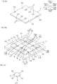
FIG. 1] FIG. 1A to FIG. 1G are perspective views illustrating process diagrams showing an embodiment of the method for producing a phosphor plate of the present invention, and the method for producing an optical semiconductor device,FIG. 1A to FIG. 1E and FIG. 1G are perspective views from above, andFIG. 1F is a perspective view from below.FIG. 1A shows a step (1), in which a greensheet is prepared,FIG. 1B shows a step (2), in which through holes and penetration faces are formed in the greensheet,FIG. 1C shows a step (4), in which the greensheet is calcined to form a ceramic plate,FIG. 1D shows a step in which the ceramic plate is supported by a supporting sheet,FIG. 1E shows a step (3), in which the ceramic plate is cut with a cutting blade,FIG. 1F shows a step (6), in which the plurality of phosphor plates are transferred from the supporting sheet to a transfer sheet, andFIG. 1G shows a step in which an optical semiconductor device is produced. - [
FIG. 2] FIG. 2A to FIG. 2C are process diagrams illustrating a modified example of the step (3) shown inFIG. 1E ,FIG. 2A showing a step in which the ceramic plate is scribed,FIG. 2B showing a step in which the ceramic plate is broken with a breaking member, andFIG. 2C showing a step in which the ceramic plate is broken with a grinding member. - [
FIG. 3] FIG. 3A and FIG. 3B are process diagrams illustrating a modified example of the step (6) shown inFIG. 1F ,FIG. 3A showing a step in which the phosphor plate is taken off from the supporting sheet and turned, andFIG. 3B showing a step (7), in which the plurality of phosphor plates are arranged on a separate supporting sheet. - [
FIG. 4] FIG. 4A to FIG. 4C are process diagrams illustrating a modified example of the step (2) and step (3) shown in shown inFIG. 1B, FIG. 1E, and FIG. 1F ,FIG. 4A showing the step (2), in which square holes, and penetration faces having a front face, rear face, and two connection faces are formed in the greensheet,FIG. 4B showing the step (3), in which the ceramic plate is cut, andFIG. 4C showing a step in which the phosphor plate is obtained. - [
FIG. 5] FIG. 5A to FIG. 5C are process diagrams illustrating a modified example of the step (2) and step (3) shown inFIG. 1B, FIG. 1E, and FIG. 1F ,FIG. 5A showing the step (2), in which square holes, and penetration faces having a front left face, a rear right face, a front right face, and a rear left face are formed in the greensheet,FIG. 5B showing the step (3), in which the ceramic plate is cut, andFIG. 5C showing a step in which the phosphor plate is obtained. - [
FIG. 6] FIG. 6A to FIG. 6C are process diagrams illustrating a modified example of the step (2) and step (3) shown inFIG. 1B, FIG. 1E, and FIG. 1F ,FIG. 6A showing a step (2), in which a plurality of through holes are formed in the greensheet,FIG. 6B showing a step (3), in which the ceramic plate is cut so that the second cutting line only has a second left-right cutting line, andFIG. 6C showing a step in which a phosphor plate having two penetration faces is obtained. - [
FIG. 7] FIG. 7A and FIG. 7B are process diagrams illustrating a modified example of the step (2) and step (3) shown inFIG. 1B, FIG. 1E, and FIG. 1F ,FIG. 7A showing a step (2), in which a plurality of through holes are formed in the greensheet,FIG. 7B showing a step (3), in which the ceramic plate is cut so that the second cutting line is not formed but only a first cutting line is formed, andFIG. 7C showing a step in which the phosphor plate having one through hole is obtained. - An embodiment of the method for producing a phosphor plate of the present invention and the method for producing an optical semiconductor device are described with reference to
FIG. 1A to FIG. 1G . In the figures, directions are in conformity with direction arrows. - A method for producing a phosphor plate includes, in sequence, a step (1) (ref:
FIG. 1A ), in which a phosphor sheet of the present invention is prepared as agreensheet 1; a step (2) (ref:FIG. 1B ), in which throughholes 2 and penetration faces 3 fronting the throughhole 2 are formed in thegreensheet 1; a step (4) (ref:FIG. 1C ), in which a phosphor plate of the present invention is formed as aceramic plate 4 produced by calcining thegreensheet 1; a step (3) (ref:FIG. 1D and FIG. 1E ), in which theceramic plate 4 is cut to form the plurality ofphosphor plates 15 including the penetration faces 3; and a step (6) (ref:FIG. 1F ), in which thephosphor plate 15 is transferred from the supportingsheet 5 to thetransfer sheet 20. - That is, in the method for producing a phosphor plate, the step (1) (ref:
FIG. 1A ), step (2) (ref:FIG. 1B ), step (4) (ref:FIG. 1C ), step (3) (ref:FIG. 1D and FIG. 1E ), and step (6) (ref:FIG. 1F ) are carried out sequentially. Each of the steps is described below. - In the step (1), as shown in
FIG. 1A , agreensheet 1 is prepared. - The
greensheet 1 can be prepared by a method such as, slurry (slip) molding; compression molding such as cold isostatic pressing (CIP) and hot isostatic pressing (HIP); and injection molding. Preferably, in view of thickness precision of thegreensheet 1, slurry molding and compression molding are used, more preferably, slurry molding is used. - In slurry molding, first, for example, a slurry containing a phosphor composition containing a phosphor material, organic particles, and a binder; and a dispersion medium is prepared.
- The phosphor material is a raw material composing phosphor, and is suitably selected in accordance with the phosphor.
- The phosphor has a function of converting wavelength, and examples thereof include yellow phosphor that can convert blue light to yellow light, and red phosphor that can convert blue light to red light.
- Examples of the yellow phosphor include silicate phosphor such as (Ba,Sr,Ca)2SiO4;Eu and (Sr,Ba)2SiO4:Eu (barium orthosilicate (BOS)); garnet phosphor having a garnet crystal structure such as (Y,Gd,Ba,Ca,Lu)3(Al,Si,Ge,B,P,Ga)5O12:Ce (YAG (yttrium • aluminum • garnet):Ce) and Tb3Al3O12: Ce (TAG (terbium • aluminum • gamet):Ce); and oxynitride phosphor such as Ca-α-SiAlON. Examples of the red phosphor include nitride phosphors such as CaAlSiN3:Eu and CaSiN2:Eu. Preferably, garnet phosphor, more preferably YAG:Ce (Y3Al5O12:Ce) is used.
- Examples of the phosphor material include a metal itself that composes phosphor, a metal oxide thereof, and a metal nitride. To be specific, examples of the phosphor material include, when YAG: Ce is formed as the phosphor, metal oxides such as a yttrium-containing compound including yttrium oxide, an aluminum-containing compound including aluminum oxide, and a cerium-containing compound including cerium oxide are used. The phosphor material is formed, for example, into particles (or powder).
- The phosphor material has a purity of, for example, 99.0 mass% or more, preferably 99.9 mass% or more.
- The organic particles are contained in the phosphor composition as necessary to form micropores (not shown) in the
ceramic plate 4. For the organic material forming the organic particles, those materials that are thermally decomposed completely in the step (4) (described later) are used, and thermoplastic resin such as acrylic resin (to be specific, polymethyl methacrylate), styrene resin, acryl-styrene resin, polycarbonate resin, benzoguanamine resin, polyolefin resin, polyester resin, polyamide resin, and polyimide resin; and thermosetting resin such as epoxy resin and silicone resin are used. Preferably, thermoplastic resin, more preferably, acrylic resin is used. The average particle size of the organic particles is not particularly limited, and for example, it is 3.4 µm or more, preferably 4.0 µm or more, and for example, 25.0 µm or less, preferably 20.0 µm or less, more preferably 8.0 µm or less. - The organic particle content relative to a total of the phosphor material content and the organic particles content is, for example, 1.5% by volume or more, preferably 2.0% by volume or more, and for example, 12.0% by volume or less, preferably 10.0% by volume or less, more preferably 8.0% by volume or less.
- Examples of the binder include resin such as acrylic polymer, butyral polymer, vinyl polymer, and urethane polymer. Examples of the binder also include water-soluble binders. Preferably, acrylic polymer, more preferably, water-soluble acrylic polymer is used. The binder content is set so that relative to 100 parts by volume of a total of the phosphor material and the binder, the binder content is, for example, 10 parts by volume or more, preferably 20 parts by volume or more, more preferably 30 parts by volume or more, and for example, 60 parts by volume or less, preferably 50 parts by volume or less, more preferably 40 parts by volume or less.
- The phosphor composition can further contain, for example, as necessary, additives such as a dispersing agent, a plasticizer, and a calcination auxiliary agent.
- The dispersion medium is not particularly limited, as long as it can disperse the phosphor material and the organic particles. Examples of the dispersion medium include water, and an organic dispersion medium such as acetone, methyl ethyl ketone, methanol, ethanol, toluene, methyl propionate, and methyl cellosolve. Preferably, water is used. The dispersion medium content relative to the slurry is, for example, 1 mass% or more, for example, 30 mass% or less.
- To prepare the slurry, first, the above-described component is blended at the above-described ratio, and the mixture is subjected to, for example, wet blending with a ball mill.
- When the slurry is prepared, the above-described component can be subjected to wet blending all at once. Alternatively, the components other than the organic particles can be subjected to wet blending to prepare a first slurry, and then, the first slurry can be blended with organic particles by wet blending to prepare a slurry.
- Then, in the step (1), the slurry is applied on the surface of the
release sheet 10, and thereafter, dried. - The
release sheet 10 is formed from a flexible material. Examples of such materials include a polyester sheet such as polyethylene terephthalate (PET) sheet; a polycarbonate sheet; polyolefin sheets such as a polyethylene sheet and a polypropylene sheet; a polystyrene sheet; an acryl sheet; and resin sheets such as a silicone resin sheet and a fluorine resin sheet. Furthermore, foil of metals such as copper foil and stainless steel foil are used. Preferably, a resin sheet, even more preferably, a polyester sheet is used. The surface of therelease sheet 10 may be treated for release in order to improve releasability, as necessary. The thickness of therelease sheet 10 is set suitably in view of handleability and costs, and is, to be specific, 10 µm or more and 200 µm or less. - The slurry is applied on the
release sheet 10 by coating methods such as doctor blade coating, gravure coating, fountain coating, cast coating, spin coating, and roll coating. - In this manner, a coating composed of slurry is formed on the surface of the
release sheet 10. - Then, the coating is dried.
- The drying temperature is, for example, 20°C or more, preferably 50°C or more, and for example, 200°C or less, preferably 150°C or less.
- The drying time is, for example, 1 minute or more, preferably 2 minutes or more, and for example, 24 hours or less, preferably 5 hours or less.
- In this manner, the
greensheet 1 supported by therelease sheet 10 is obtained. - The
greensheet 1 is a sheet before calcining the ceramic plate 4 (ref:FIG. 1C ), and is a plate extending in front-back directions and left-right directions. - Thereafter, the
release sheet 10 is released from thegreensheet 1. - Thereafter, as necessary, to obtain a desired thickness, a plurality of (a plurality of layers of) greensheets 1 can be laminated by heat lamination to obtain a
greensheet laminate 1. - The greensheet 1 (or greensheet laminate 1) has a thickness T1 of, for example, 10 µm or more, preferably 30 µm or more, and for example, 500 µm or less, preferably 200 µm or less.
- In this step (2), as shown in
FIG. 1B , throughholes 2 are formed in thegreensheet 1. - In the
greensheet 1, the plurality of throughholes 2 are arranged in line in front-back directions and left-right directions in spaced-apart relation to each other (2 rows in front-back directions and 2 rows in left-right directions). The plurality of throughholes 2 are round holes that penetrates thegreensheet 1 in the thickness direction (up-down direction). - The step (2) can be conducted by methods of making holes such as the following: for example, the
greensheet 1 can be subjected to punching, blast processing, drilling, or laser processing with, for example, YAG laser. - For the blast processing, for example, direct pressure blast processing and siphon processing can be used. In blast processing, to be specific, in the
greensheet 1, a resist is placed so as to cover the portions excluding the portions where throughholes 2 are made, and then a blasting material isgreensheet 1 is applied. The size of the throughhole 2 is suitably adjusted by suitably adjusting the types and particle size of the blasting material used for blast processing, and the speed of blasting, or type (direct pressure ,siphon). - Blast processing is preferable in view of productivity, compared with laser processing.
- To carry out the step (2), in view of shortening takt time and reducing processing costs, preferably, the
greensheet 1 is punched or thegreensheet 1 is drilled. - When the
greensheet 1 is subjected to drilling, since a drill has a small diameter and easily damaged (broken), and therefore to prevent such problems, drilling process takes long time. Therefore, in view of shortening the takt time, more preferably, thegreensheet 1 is punched. - Then, by forming the plurality of through
holes 2 in thegreensheet 1, a plurality of penetration faces 3 fronting of the plurality of throughholes 2 are formed in thegreensheet 1. That is, in the step (2), the throughholes 2 and the penetration faces 3 are formed simultaneously. - The
penetration face 3 are inner periphery of the throughhole 2 extending in the thickness direction (up-down direction) in thegreensheet 1. - The size of the through
hole 2 and thepenetration face 3 is suitably set in accordance with the size of theconnection portion 25 and the wire 29 (ref:FIG. 1G ) of theoptical semiconductor device 30 described later. To be specific, the throughhole 2 has an internal diameter L1 of, for example, 0.1 mm or more, preferably 0.3 mm or more, and for example, 5.0 mm or less, preferably 1.0 mm or less. The interval L2 between the throughholes 2 that are adjacent in front-back directions and left-right directions is, for example, 0.5 mm or more, preferably 1.0 mm or more, and for example, 20 mm or less, preferably 10 mm or less. The pitch L3 of the throughholes 2 that are adjacent to each other, that is, a sum of the internal diameter L1 and the interval L2 of the throughhole 2 is, for example, 0.1 mm or more, preferably 1 mm or more, and for example, 20 mm or less, preferably 10 mm or less. - In the step (4), as shown in
FIG. 1C , the greensheet 1 (ref:FIG. 1B ) is calcined. - The calcination temperature is, for example, 1300°C or more, preferably 1500°C or more, and for example, 2000°C or less, preferably 1800°C or less.
- The calcination time is, for example, 1 hour or more, preferably 2 hours or more, and for example, 24 hours or less, preferably 8 hours or less.
- The speed of the temperature increase in calcination is, for example, 0.5°C/minutes or more, and 20°C/ minutes or less.
- To subject the organic components such as a binder and a dispersing agent to thermal decomposition and to remove them, before the above-described calcination (main calcination), organic component removal processing can also be performed by preheating in air at, for example, 600°C or more and 1300°C or less using an electric furnace.
- By calcination of the above-described
greensheet 1, aceramic plate 4 having the throughholes 2 and penetration faces 3 is produced. - The ceramic plate 4 (ref:
FIG. 1 C) after calcining shrinks compared with the greensheet 1 (FIG. 1B ) before calcination. For example, the thickness T1, the internal diameter L1 of the throughhole 2, interval L2 between the throughholes 2 that are adjacent to each other, and pitch L3 between the throughholes 2 that are adjacent to each other in theceramic plate 4 after calcinations is, for example, 99% or less, preferably 95% or less, more preferably 90% or less, and 60% or more relative to T1, L1, L2 and L3 of thegreensheet 1 before calcination. - To be specific, the
ceramic plate 4 after calcination has a thickness T1 of, for example, 0.03 mm or more, preferably 0.05 mm or more, and for example, 1.0 mm or less, preferably 0.3 mm or less. The internal diameter L1 of the throughhole 2 of theceramic plate 4 after calcinations is, for example, 0.1 mm or more, and for example, 1.0 mm or less, preferably 0.5 mm or less. The interval L2 between the throughholes 2 that are adjacent to each other in front-back directions and left-right directions in theceramic plate 4 after calcination is, for example, 0.5 mm or more, preferably 1.0 mm or more, and for example, 20 mm or less, preferably 10 mm or less. The pitch L3 between the throughholes 2 in theceramic plate 4 after calcination is, for example, 0.6 mm or more, preferably 1.1 mm or more, and for example, 20.5 mm or less, preferably 10.5 mm or less. - In the
ceramic plate 4, a plurality of micropores (not shown) are formed. The pores have an average pore size of, for example, 2.5 (µm or more, preferably 3.0 µm or more, more preferably 3.5 µm or more, and for example, 20.0 µm or less, preferably 16.0 µm or less, more preferably 10.0 µm or less. - In the step (3), as shown in
FIG. 1D and FIG. 1E , theceramic plate 4 is cut to form a plurality of phosphor plates including thepenetration face 3. - In this step (3), as shown in
FIG. 1D , first, theceramic plate 4 is supported by the supportingsheet 5. - For the supporting
sheet 5, a slightly adhesive dicing tape that can support the supportingsheet 5 to reliably cut theceramic plate 4 and thereafter to release the ceramic plate 4 (to be specific,phosphor plate 15 described later) after cutting is used. The size of the supportingsheet 5 is suitably adjusted in accordance with the size of theceramic plate 4, and for example, the length in front-back directions and the length in left-right directions of the supportingsheet 5 are longer relative to those of theceramic plate 4. - Then, in the step (3), as shown in
FIG. 1E , thegreensheet 1 is cut with acutting blade 6. - For the cutting blade, as shown in
FIG. 1E , for example, a dicing saw (dicing blade) 7 having a disc shape and is rotatable around its axis, and for example, a cutter (not shown) having a generally horizontal edge is used. For thecutting blade 6, preferably, a dicing saw 7 is used. - To cut the
ceramic plate 4, to be specific, for example, a dicing device including the dicing saw 7, and a cutting device (not shown) having a cutter is used. Preferably, a dicing device is used. - Then, the
ceramic plate 4 is cut so that thefirst cutting line 11 as an example of cutting lines formed with the above-describedcutting blade 6 pass through the plurality of throughholes 2, thereby producing thephosphor plate 15. To be specific, theceramic plate 4 is cut so that thepenetration face 3 defining one throughhole 2 is given to the plurality ofphosphor plates 15 and onepenetration face 3 is divided. To be specific, theceramic plate 4 is cut so that thepenetration face 3 defining one throughhole 2 is given to fourphosphor plates 15 and onepenetration face 3 is divided into four. - To be specific, the
ceramic plate 4 is cut so that thefirst cutting lines 11 pass through the centers of the plurality of throughholes 2. Then, onepenetration face 3 is divided into a plural number. - The
first cutting line 11 has first front-back cutting lines 12 extending in front-back directions and arranged in left-right directions in spaced-apart relation to each other, and first left-right cutting lines 13 extending in left-right directions and arranged in front-back directions in spaced-apart relation to each other. - The first front-
back cutting lines 12 and the first left-right cutting lines 13 orthogonally cross each other at the centers of the plurality of throughholes 2. - Along with cutting of the
ceramic plate 4 along thefirst cutting line 11, cutting of theceramic plate 4 along thesecond cutting line 14 is performed. - The
second cutting lines 14 do not pass the through holes 2. To be specific, thesecond cutting lines 14 pass between the through holes 2. Thesecond cutting lines 14 have second front-back cutting lines 16 extending in front-back directions and are parallel and adjacent to the first front-back cutting lines 12, and second left-right cutting lines 17 extending in left-right directions and are parallel and adjacent to the first left-right cutting lines 13. - The second front-
back cutting lines 16 and the first front-back cutting lines 12 are arranged alternatively in left-right directions at an equal interval. The second left-right cutting line 17 and the first left-right cutting line 13 are arranged alternatively in front-back directions at an equal interval. - The
ceramic plate 4 is cut so that the lower end portion of thecutting blade 6 goes into the supportingsheet 5. Therefore, cuttinggrooves 21 corresponding to thefirst cutting lines 11 and thesecond cutting lines 14 are formed at the upper portion of the supportingsheet 5. - Then, by cutting the
ceramic plate 4 along the above-described first cuttingline 11 and thesecond cutting line 14, the plurality ofphosphor plates 15 are produced while they are supported on the upper face of the supportingsheet 5. - The
phosphor plate 15 has a plate shape having a flat upper face and a flat lower face. The side face of thephosphor plate 15 has apenetration face 3 divided (given) from onepenetration face 3, two first side faces 18 (two faces) that are continuous with the end portion of thepenetration face 3 and along thefirst cutting line 11, and two second side faces 19 (two faces) that are continuous with the end portion of thefirst side face 18 and along thesecond cutting line 14. - To be specific, in the
first phosphor plate 15A (ref: hatched portion inFIG. 1E ) that is positioned at the center (portion excluding the peripheral end portion to be described later) of the supportingsheet 5 and in which thepenetration face 3 is formed at the rear left side face, thefirst side face 18 along the first front-back cutting line 12 is continuous with the front end portion of thepenetration face 3, and thefirst side face 18 along the first left-right cutting line 13 is continuous with the rear end portion of thepenetration face 3. Thesecond side face 19 along the second front-back cutting line 16 is continuous with the right end portion of thefirst side face 18 between the first left-right cutting line 13, and thesecond side face 19 along the second left-right cutting line 17 is continuous with the front end portion of thefirst side face 18 along the first front-back cutting line 12, and the front end portion of thesecond side face 19 along the second front-back cutting line 16. Thepenetration face 3 of thephosphor plate 15 and the side faces of thefirst side face 18 and thesecond side face 19 are in continuous with each other in this way. - Meanwhile, the
second phosphor plate 15B positioned at the peripheral end portion of the supportingsheet 5 has, at least, twofirst cutting lines 11 and one peripheral face corresponding to the peripheral face of theceramic plate 4. Thesecond phosphor plate 15B includes a plurality of (4) third phosphor plates 15B3 and a plurality of fourth phosphor plates 15B4. The third phosphor plate 15B3 is positioned at the corner portion of the supportingsheet 5, and two first cutting lines 11 (to be specific, one first front-back cutting line 12 and one first left-right cutting line 13) and two peripheral faces corresponding to the peripheral face of theceramic plate 4. The fourth phosphor plate 15B4 is positioned between the third phosphor plates 15B3, and has twofirst cutting lines 11 and one second cutting line 14 (second front-back cutting line 16 or second left-right cutting line 17), and one peripheral face corresponding to the peripheral face of theceramic plate 4. - The size of the plurality of
phosphor plates 15 is suitably set in accordance with the size of the optical semiconductor element 28 (ref:FIG. 1G ) to be described later. Thephosphor plate 15 has a length in front-back directions and a length in left-right directions of, relative to the length in front-back directions and the length in left-right directions of the penetration face 3 (that is, half of the internal diameter L1 of through hole 2), for example, twice or more, preferably four times or more, and for example, 20 times or less, preferably 10 times or less. To be specific, thephosphor plate 15 has a length in front-back directions and a length in left-right directions of, for example, 0.1 mm or more, preferably 0.5 mm or more, and for example, 10 mm or less, preferably 2.0 mm or less. - In the step (6), as shown in
FIG. 1F , the plurality ofphosphor plates 15 are transferred from the supportingsheet 5 to thetransfer sheet 20. - To transfer the plurality of
phosphor plates 15 from the supportingsheet 5 to thetransfer sheet 20, for example, first, thetransfer sheet 20 is prepared, and thetransfer sheet 20 is disposed on the plurality ofphosphor plates 15 to face the phosphor plates. - The
transfer sheet 20 can stretch in front-back directions and left-right directions (surface direction), and has slight adhesiveness. The size of thetransfer sheet 20 is set suitably in accordance with the size of the plurality ofphosphor plates 15, and has a longer length in front-back directions and length in left-right directions relative to a total of the length in front-back directions of the plurality oftransfer sheets 20, and a total of the length in left-right directions of the plurality oftransfer sheets 20. - Then, the lower face of the
transfer sheet 20 is allowed to contact the upper face of the plurality ofphosphor plates 15, and then, the plurality ofphosphor plates 15 are removed from the supportingsheet 5. In this manner, the plurality ofphosphor plates 15 are transferred from the supportingsheet 5 to thetransfer sheet 20. That is, the plurality ofphosphor plates 15 are temporarily fixed to thetransfer sheet 20. - In this manner, the plurality of
phosphor plates 15 are produced while temporarily fixed to thetransfer sheet 20. - The
phosphor plate 15 is not theoptical semiconductor element 28 to be described in nextFIG. 1G . Thephosphor plate 15 is one component of theoptical semiconductor device 30, that is, a component to produce theoptical semiconductor device 30, and does not include theoptical semiconductor element 28. Thephosphor plate 15 is distributed singly as a component, and is an industrially applicable device, but is not thereto. - Thereafter, an
optical semiconductor device 30 is produced using thephosphor plate 15. - To be specific, first, as shown in
FIG. 1F , each of the plurality ofphosphor plates 15 is taken off from thetransfer sheet 20 with, for example, a pick-up device (not shown) including a collet, and then, as shown inFIG. 1G , piled on the upper face of theoptical semiconductor element 28. - The
optical semiconductor element 28 is included in theoptical semiconductor device 30. - The
optical semiconductor device 30 includes asubstrate 26, a terminal 27, anoptical semiconductor element 28, aphosphor plate 15, and awire 29. - The
substrate 26 has a generally plate shape, and is composed of an insulating material. - The terminal 27 is disposed on the upper face of the
substrate 26. - The
optical semiconductor element 28 is fixed on the upper face of thesubstrate 26, and is disposed in spaced-apart relation with the terminal 27. Theoptical semiconductor element 28 has a generally plate shape, and is composed of an optical semiconductor material. On the corner portion of the upper face of theoptical semiconductor element 28, aconnection portion 25 is formed. - The
phosphor plate 15 is disposed on the upper face of theoptical semiconductor element 28 so as to expose theconnection portion 25. Thephosphor plate 15 is allowed to adhere to the upper face of theoptical semiconductor element 28 through an adhesive, that is not shown. - The
wire 29 is disposed so that it is bent toward upper side. Thewire 29 bends in generally letter U shape with its opening toward below. One end portion of thewire 29 is connected to theconnection portion 25, and the other end of thewire 29 is connected to the terminal 27. That is, thewire 29 allows connection between theconnection portion 25 and the wire 29 (wire bonding). Thewire 29 is disposed to detour thephosphor plate 15. - To produce the
optical semiconductor device 30, first, asubstrate 26 in which a terminal 27 and anoptical semiconductor element 28 are disposed is prepared. Then, the lower face of thephosphor plate 15 is allowed to adhere to the upper face of theoptical semiconductor element 28 through an adhesive, which is not shown. At this time, thephosphor plate 15 is piled on theoptical semiconductor element 28 so as to expose theconnection portion 25 from thepenetration face 3. Thereafter, theconnection portion 25 is connected to the terminal 27 through the wire 29 (wire bonding). - The description above is an example, and for example, the method can be suitably and accordingly changeable. For example, the
phosphor plate 15 and theoptical semiconductor element 28 are joined, and thereafter they can be disposed to thesubstrate 26. - With the method, without molding the bar shaped shaped-body as described in the method in
Patent Document 1, as shown inFIG. 1A , first, thegreensheet 1 is prepared, and then, as shown inFIG. 1B , throughholes 2 are formed in thegreensheet 1, and then, as shown inFIG. 1E , theceramic plate 4 produced from thegreensheet 1 is cut. Therefore, the throughholes 2 can be formed easily, and thephosphor plate 15 can be produced with excellent production efficiency. - With the method, by cutting the
ceramic plate 4 having thefirst cutting line 11, thepenetration face 3 is divided to (4) so that thepenetration face 3 defining one throughhole 2 is given to a plurality of (4)phosphor plates 15. Thus, production efficiency is even more excellent. - In this method, the phosphor sheet composed of the
greensheet 1 can be prepared, and thephosphor plate 15 composed of theceramic plate 4 can be produced. - As shown in
FIG. 1E , when the supportingsheet 5 has scrapes caused by cutting (not shown inFIG. 1E ) and/or when the supportingsheet 5 has cuttinggrooves 21, in later steps, to be specific, when thephosphor plate 15 is taken off with a pick-up device, the scrapes and/or cuttinggroove 21 may give effects (for example, to taking off of thephosphor plate 15 with a pick-up device). - However, as shown in
FIG. 1F , after the step (3), by transferring the plurality ofphosphor plates 15 from the supportingsheet 5 to thetransfer sheet 20, the above-described effects can be excluded. - When the method in which the
ceramic plate 4 is cut with acutting blade 6, theceramic plate 4 can be reliably cut. - In the step (2), by carrying out any one of the following methods, the through
holes 2 can be reliably formed in thegreensheet 1 while achieving shortening of takt time and reduction of processing costs: a method in which thegreensheet 1 is punched, a method in which thegreensheet 1 is subjected to blast processing, a method in which thegreensheet 1 is subjected to laser processing, and a method in which thegreensheet 1 is subjected to drilling. - In Modified Examples, those members and steps that are the same as the embodiment above, the same reference numerals are given and detailed descriptions thereof are omitted.
- In one embodiment, as shown in
FIG. 1E , theceramic plate 4 is cut so that the second front-back cutting line 16 is singular, but for example, although not shown, theceramic plate 4 can be cut so that the second front-back cutting line 16 is in a plural number. In the case of the above, in the step (2), the throughholes 2 are arranged, for example, so that there are three or more left-right rows in thegreensheet 1, and in the step (3), the second front-back cutting line 16 is formed between every two adjacent throughholes 2 arranged in left-right directions. - In one embodiment, as shown in
FIG. 1E , theceramic plate 4 is cut so that the second left-right cutting line 17 is singular, but for example, although not shown, theceramic plate 4 can be cut so that the second left-right cutting line 17 is in a plural number. In this case, in the step (2), the throughholes 2 are arranged, for example, so that there are three or more front-rear rows in thegreensheet 1, and in the step (3), the second left-right cutting line 17 is formed between every two adjacent throughholes 2 in front-back directions. - Although not shown, for example, the through
hole 2 can be singular. - In one embodiment, as shown in
FIG. 1E , onepenetration face 3 is divided into 4. However, the number of division of thepenetration face 3 is not particularly limited. Although not shown, for example, it can be divided to 2, 3, 5, 6, or 7. - In one embodiment, in the step (3), as shown in
FIG. 1E , theceramic plate 4 is cut with acutting blade 6, but for example, as shown inFIG. 2A and FIG. 2B , theceramic plate 4 can be scribed or broken. - In this method, first, as shown in
FIG. 2A , the upper portion of theceramic plate 4 is scribed (shaved) along thefirst cutting line 11 and thesecond cutting line 14. - To scribe the
ceramic plate 4, the dicing saw 7 (ref: solid line) and the cutter 8 (ref: phantom line) are used. Thecutter 8 has acutting edge 48 that is movable in up-down direction. Thecutting edge 48 is parallel to the upper face of theceramic plate 4. - In this manner, the
groove 22 corresponding to thefirst cutting line 11 and thesecond cutting line 14 are formed on the upper portion of theceramic plate 4. Thegroove 22 has a cross section of generally V shape with its opening facing upward. Thegroove 22 has a depth of, for example, 1 µm or more, preferably 3 µm or more, and for example, 20 µm or less, preferably 10 µm or less. - Thereafter, as shown in
FIG. 2B , theceramic plate 4 is broken along with thegroove 22. - To break the
ceramic plate 4, a breakingmember 23 sharpened downward is pressed against thegroove 22, and the breakingmember 23 is pressed downward. - Alternatively, as shown in
FIG. 2C , while pressing the upper face of theceramic plate 4 with a grindingmember 24 having a flat lower face and a disc shape, the grindingmember 24 is allowed to grind in front-back directions and left-right directions (grind breaking). Then, when the end portion of the lower face of the grindingmember 24 is overlapped with the position of thegroove 22, the pressured applied from the grindingmember 24 is concentrated on thegroove 22, and breaks the ceramic plate 4 (breaking) positioned below thegroove 22. - In this manner, the
ceramic plate 4 is broken along thegroove 22. - Furthermore, instead of or in addition to cutting with a cutting blade, scribing, and breaking, the
ceramic plate 4 can be cut by laser. - Examples of the laser include YAG laser and CO2 laser, and preferably, YAG laser is used.
- Alternatively, instead of or in addition to cutting with a cutting blade, scribing, and breaking, the
ceramic plate 4 can be cut by blast processing. - Examples of blast processing include direct pressure blast processing and siphon processing. In blast processing, to be specific, in the
ceramic plate 4, the portion other than the portion forming thefirst cutting line 11 and thesecond cutting line 14 is covered with a resist, and then a blasting material is applied to theceramic plate 4. By suitably changing the types, particle size, blasting speed, and types (direct pressure, siphon) of the blasting material used in the blast processing, the size of thefirst cutting line 11 and thesecond cutting line 14 can be suitably adjusted. - Blast processing is preferable in view of productivity compared with laser processing.
- In the step (3), of the following methods, i.e., a method in which the
ceramic plate 4 is cut with a cutting blade, a method in which theceramic plate 4 is scribed and broken, a method (laser processing) in which theceramic plate 4 is cut by laser, and a method in which theceramic plate 4 is subjected to blast processing, preferably, to prevent melting mark (to be specific, laser abrasion mark) to remain at the side face of thephosphor plate 15 caused by heat along with laser irradiation, preferably, theceramic plate 4 is cut with a cutting blade, or theceramic plate 4 is scribed or broken. - In the step (3), more preferably, in view of accuracy in size of the
phosphor plate 15, theceramic plate 4 is cut with a cutting blade. - In one embodiment, as shown in
FIG. 1E and FIG. 1F , after the step (3), a step (6), in which a plurality ofphosphor plates 15 are transferred from the supportingsheet 5 to thetransfer sheet 20, is carried out. Instead, for example, as shown inFIG. 3A , a step (7), in which the plurality ofphosphor plates 15 are taken off from the supportingsheet 5, and then as shown inFIG. 3B , the plurality ofphosphor plates 15 are arranged so that the penetration faces 3 of thephosphor plate 15 are oriented in the same direction can be conducted. - In this method, first, as shown in
FIG. 3A , the plurality ofphosphor plates 15 are taken off from the supportingsheet 5 using a pick-updevice 44, and then disposed on the surface of another supportingsheet 35. - The pick-up
device 44 extends in up-down direction, and has acollet 45 having a suction port at its lower face. Thecollet 45 is configured to be rotatable around the axis extending in up-down direction. Then, the suction port of thecollet 45 is allowed to contact the upper face of thephosphor plate 15 and to suck thephosphor plate 15, and then thephosphor plate 15 is pulled up, and thereafter, the collet is rotated to a desired angle (revolution). Thereafter, the plurality ofphosphor plates 15 are arranged on the surface of another supportingsheet 35 so that thepenetration face 3 of the plurality ofphosphor plates 15 are oriented toward the same direction, for example, obliquely front-right side. - The plurality of
phosphor plates 15 are arranged on the surface of another supportingsheet 35, with an interval L4 between each other in, for example, front-back directions and left-right directions. - Another supporting
sheet 35 is formed from the same material as that of the supportingsheet 5. - Then, in this method, when the plurality of
phosphor plates 15 are taken off from the supportingsheet 5 and the plurality ofphosphor plates 15 are arranged so that their penetration faces 3 are oriented toward the same direction after the step (3), handleability of the plurality ofphosphor plates 15 can be improved. - In the description above, the step (6) and the step (7) are carried out selectively, but the step (6) and the step (7) can be carried out both.
- In one embodiment, in the step (2), as shown in
FIG. 1B , the throughholes 2 have a round shape, but the shape of the throughhole 2 is not particularly limited. The throughholes 2 can be formed, for example, into a polygon, to be specific, as shown inFIG. 4A andFIG. 5A , the throughholes 2 can be formed into a rectangular shape. That is, the throughholes 2 can be square holes. - As shown in
FIG. 4A , thepenetration face 3 fronting the throughhole 2 has afront face 31 and arear face 32 facing each other in front-back directions, and two connection faces 33 connecting their left-right both end portions. Thefront face 31 and therear face 32 extend in left-right directions. The two connection faces 33 extend in front-back directions. - The length in front-back directions and length in left-right directions L1 of the through
hole 2 are the same as the internal diameter L1 of the round hole in one embodiment. - In the step (3), as shown in
FIG. 4B , by cutting thegreensheet 1, thepenetration face 3 is divided into a plurality of (4)phosphor plates 15. - Then, as shown in
FIG. 4C , thephosphor plate 15 has a generally letter L shape when viewed from the top. - Alternatively, as shown in
FIG. 5A , thepenetration face 3 fronting the throughhole 2 continuously has a frontleft face 37 and a rearright face 38 facing each other in a first inclination direction ID1, which inclines leftward as it approaches the front side, and a frontright face 39 and a rearleft face 40 connecting the front-back end portions of the frontleft face 37 and rearright face 38 and facing each other in a second inclination direction (direction which inclines rightward as it approaches the front side) ID2, which orthogonally crosses the first inclination direction ID1. - The length of the front
left face 37 and the rear right face 38 (length along the first inclination direction ID2) L5 may be the same or different from the length of the frontright face 39 and the rear left face 40 (length along the second inclination direction ID1) L5, and relative to the above-described L1, for example, 50% or more, preferably 65% or more, and for example, 200% or less, preferably 100% or less. To be specific, the L5 is, for example, 0.05 mm or more, preferably 0.1 mm or more, and for example, 5 mm or less, preferably 1 mm or less. - In the step (3), as shown in
FIG. 5B , by cutting thegreensheet 1, the frontleft face 37, rearright face 38, frontright face 39, and rearleft face 40 are given to a plurality of (4)phosphor plates 15. - Then, the
phosphor plate 15 has a generally pentagon shape, and has aninclination face 36 formed from one of the frontleft face 37, rearright face 38, frontright face 39, and rearleft face 40. - In one embodiment, one
phosphor plate 15 has onepenetration face 3. However, the number of thepenetration face 3 is not particularly limited. For example, as shown inFIG. 6C , onephosphor plate 15 may have a plurality of penetration faces 3. - In the step (2), as shown in
FIG.6A , in thegreensheet 1, the plurality of throughholes 2 andcutouts 52 are arranged in line, 2 rows in front-rear (n rows) and 4 rows in left-right (2n rows). Thecutouts 52 have a semicircle shape, in which the right side face or the left side face of theceramic plate 4 is cut out. - Then, as shown in
FIG. 6B , in the step (3), theceramic plate 4 is cut so that two penetration faces 3 adjacent to each other in left-right directions are divided and given to at least onephosphor plate 15. - In this step (3), as shown in
FIG. 6B , thesecond cutting line 14 does not have the second front-back cutting line 16 (ref:FIG. 1F ), but only has a second left-right cutting line 17. - The
phosphor plate 15 has, as shown inFIG. 6C , a plurality of (two) penetration faces 3. In thephosphor plate 15, two penetration faces 3 are connected by the first cutting line 11 (to be specific, first left-right cutting line 13). The two penetration faces 3 are disposed adjacent to each other in thephosphor plate 15 in the left-right directions. - In one embodiment, in the step (3), as shown in
FIG. 1E , theceramic plate 4 is cut so that thefirst cutting line 11 passes through the throughhole 2. However, without limitation to the above, for example, as shown inFIG. 7B , theceramic plate 4 can be cut so that only thesecond cutting line 14 passing between the throughholes 2 adjacent to each other, not passing the throughhole 2 can be formed without forming thefirst cutting line 11. - As shown in
FIG. 7B , thesecond cutting line 14 passes between the adjacent throughholes 2. - As shown in
FIG. 7C , thephosphor plate 15 has a throughhole 2 at an end portion (corner portion), and has a generally rectangular contour. Onephosphor plate 15 includes one throughhole 2. - In one embodiment, in the step (1), as shown in
FIG. 1A , the phosphor sheet of the present invention is agreensheet containing phosphor 1, and in the step (4), as shown inFIG. 1C , the phosphor sheet of the present invention is aceramic plate 4 produced by calcining thegreensheet 1. - However, as shown in reference numeral in parenthesis in
FIG. 1A , in the step (1), the phosphor sheet of the present invention can be a B-STAGE sheet 41 composed of a phosphor resin composition containing phosphor and thermosetting resin, and as shown in the reference numerals in parentheses inFIG. 1C , in the step (4), the phosphor sheet of the present invention can be aC stage sheet 42 produced by thermosetting the B-STAGE sheet 41. - The mixing ratio of the phosphor relative to the phosphor resin composition is, for example, 5 mass% or more, preferably 10 mass% or more, and for example, 80 mass% or less, preferably 70 mass% or less.
- Examples of the thermosetting resin include 2-stage reaction curable resin and 1-stage reaction curable resin.
- The 2-stage reaction curable resin has two reaction mechanisms, and in the first stage reaction, A-stage state can be changed into B-stage state (semicured), and then, in the second stage reaction, B-stage state can be changed into C-stage state (completely cured). That is, the 2-stage reaction curable resin is a thermosetting resin that can be brought into B-stage state with suitable heating conditions. The B-stage state is a state in which the thermosetting resin is in between the liquid A stage state and completely cured C stage state. In this state, curing and gelation progress slightly in the thermosetting resin, and the thermosetting resin is in semisolid or solid state having a compressive modulus smaller than the modulus of elasticity of C stage state resin.
- The 1-stage reaction curable resin has one reaction mechanism, and in the first stage reaction, the status changes from A stage status to C stage status (completely cured). Such 1-stage reaction curable resin is a thermosetting resin in which reaction stops in the middle of the first stage reaction, and which can be brought into B-stage state from A stage state. With further reaction thereafter, the first reaction restarts and the thermosetting resin can be brought into C stage (completely cured) from B-stage state. That is, the thermosetting resin is a thermosetting resin that can be brought into B-STAGE state. Therefore, the 1-stage reaction curable resin cannot be controlled to stop the reaction in the middle of the first stage, that is, cannot be brought into B-STAGE state, and does not include curable resin that can be brought into C stage state (completely cured) all at once from A stage state.
- In sum, the thermosetting resin is a thermosetting resin that can be brought into B-STAGE state.
- Examples of the thermosetting resin include silicone resin, epoxy resin, urethane resin, polyimide resin, phenol resin, urea resin, melamine resin, and unsaturated polyester resin. For the thermosetting resin, preferably, silicone resin, and epoxy resin are used, more preferably, silicone resin, even more preferably, phenyl silicone resin is used. The above-described thermosetting resin can be the same type or a plurality of different types can be used.
- The mixing ratio of the thermosetting resin is the remaining portion of the phosphor.
- In the step (1), first, the phosphor resin composition is prepared. To prepare the phosphor resin composition, the above-described phosphor is blended with the thermosetting resin, thereby preparing varnish of the phosphor resin composition.
- Then, the varnish is applied on the surface of the
release sheet 10. Thereafter, the phosphor resin composition is heated (baked). The B-STAGE sheet 41 is prepared in this manner. - Thereafter, the B-
STAGE sheet 41 is taken off from therelease sheet 10. - Then, as shown in
FIG. 1B , the step (2) is curried out. Preferably, thegreensheet 1 is punched, or thegreensheet 1 is drilled. - Thereafter, as shown in
FIG. 1C , in the step (4), the B-stage sheet 41 is thermally cured.A C stage sheet 42 is produced. - In one embodiment, as shown in
FIG. 1B to FIG. 1E , the step (2) and the step (4) are carried out in sequence. That is, first, as shown inFIG. 1B , throughholes 2 are formed in thegreensheet 1, and thereafter, as shown inFIG. 1C , thegreensheet 1 is aceramic plate 4. - However, although not shown, the step (4) and the step (2) can be carried out in sequence. That is, although not shown, first, the
greensheet 1 is aceramic plate 4, and then, the throughholes 2 are formed in theceramic plate 4. - At this time, in the step (2), the through
holes 2 can be formed in theceramic plate 4 by, for example, in one embodiment, throughholes 2 are formed in thegreensheet 1, and preferably, blast processing and laser processing are used. These may be used singly, or may be used in combination. With blast processing or laser processing, throughholes 2 and penetration faces 3 can be reliably formed in a hardceramic plate 4. - Blast processing is preferable compared with laser processing, in view of productivity. Examples
- The specific numeral values such as mixing ratio (content), physical property values, and parameters used in the following description can be replaced with upper limit value (numeral values defined with "or less", "less than") or lower limit value (numeral values defined with "or more", "more than") of corresponding mixing ratio (content), physical property values, and parameters in the above-described "DESCRIPTION OF EMBODIMENTS".
- A phosphor material powder composed of 11.34 g of yttrium oxide particles (purity 99.99%, manufactured by Nippon Yttrium Co., Ltd.), 8.577 g of aluminum oxide particles (purity 99.99%, manufactured by Sumitomo Chemical Co., Ltd.), and 0.087 g of cerium oxide particles was prepared.
- Then, 20 g of the phosphor material powder was mixed with water-soluble binder ("WB4101 ", manufactured by Polymer Inovations, Inc) so that the solid content volume ratio was 62:38, and distilled water was added thereto. The mixture was put into an alumina-made vessel, and subjected to wet blending with zirconia balls with a diameter of 3 mm for 24 hours in a ball mill, thereby preparing a first slurry.
- Then, organic particles (polymethyl methacrylate, average particle size 3.5 µm) were added to the first slurry so that the organic particles relative to a total of the phosphor material and organic particles was 3.0% by volume. The mixture was further subjected to wet blending, thereby preparing a slurry.
- Then, as shown in the phantom line and solid line in
FIG. 1A , the slurry was applied on the surface of therelease sheet 10 composed of a PET sheet by doctor blade method, and dried at 70°C for 5 minutes, thereby producing agreensheet 1 having a thickness of 55 µm. - Thereafter, the
greensheet 1 was removed from the PET sheet, and then thegreensheet 1 was cut into a size of 20 mm × 20 mm. Twogreensheets 1 after cutting were piled, and they were subjected to heat lamination using a hot press, thereby producing agreensheet laminate 1 having a thickness of 110 µm. - As shown in
FIG. 1B , a plurality of throughholes 2 and a plurality of penetration faces 3 were formed in thegreensheet laminate 1. To be specific, thegreensheet laminate 1 was drilled with a NC drill machine having a drill with a diameter of 0.7 mm manufactured by Via Mechanics, Ltd., thereby making holes in thegreensheet laminate 1. - In this manner, through
holes 2 having a round shape, an internal diameter L1 of 0.7 mm, an interval L2 of 1.7 mm, and a pitch L3 of 2.4 mm were formed in thegreensheet laminate 1. - The
greensheet laminate 1 was heated (preheating) in an electric muffle furnace in air at a temperature increase speed of 2°C/min to 1200°C, thereby thermally decomposing and removing the water-soluble binder and organic particles. - Thereafter, the
greensheet laminate 1 was transferred to a high temperature furnace, heated under reduction atmosphere at a temperature increase speed of 5°C/min to 1800°C, and calcined at the temperature for 5 hours, thereby producing aceramic plate 4 having a thickness of 120 µm as shown inFIG. 1C . - The
ceramic plate 4, i.e., after calcination, shrank about 16% relative to thegreensheet laminate 1, i.e., before calcination, to be specific, the throughholes 2 in the calcinedceramic plate 4 had an internal diameter L1 of 0.6 mm, and the interval L2 between adjacent throughholes 2 was 1.4 mm. - Thereafter, as shown in
FIG. 1D , theceramic plate 4 was temporarily fixed to the surface of the supportingsheet 5 of dicing tape. - Then, they were set in a dicing device having a dicing saw 7, and as shown in
FIG. 1E , cut with a dicing saw 7 having a blade thickness of 100 µm to pass through the center of the throughhole 2. - For the dicing device, DFD 6361 manufactured by Disco Corporation was used.
- Thereafter, as shown in
FIG. 1F , the plurality ofphosphor plates 15 were transferred from the supportingsheet 5 to the transfer sheet 20 (temporarily fixed). - In this manner, the plurality of
phosphor plates 15 fixed temporarily onto thetransfer sheet 20 were produced. - A plurality of
phosphor plates 15 were produced in the same manner as in Example 1, except that holes were made in thegreensheet laminate 1 in the step (2) by, instead of drilling, subjecting thegreensheet laminate 1 to laser processing. - In the laser processing, Model 5330 UV-YAG laser manufactured by Electro Scientific Industries, Inc. was used.
- A plurality of
phosphor plates 15 were produced in the same manner as in Example 1, except that holes were made in thegreensheet laminate 1 by punching thegreensheet laminate 1 instead of drilling in the step (2). - In the punching, a punching machine of MP series manufactured by UHT Corporation was used.
- A plurality of
phosphor plates 15 were produced in the same manner as in Example 1, except that holes were made in thegreensheet laminate 1 by punching thegreensheet laminate 1 instead of drilling, and the shape of the throughholes 2 was changed from the round shape to the rectangular shape shown inFIG. 5A in the step (2). - In the punching, MP series manufactured by UHT Corporation were used.
- The
penetration face 3 having front leftface 37, rearright face 38, frontright face 39, and rearleft face 40 was fronting the throughhole 2. - The through
hole 2 had a length in front-back directions (diagonal length) and a length in left-right directions (diagonal length) L1 of 1.0 mm, and the length of the frontleft face 37 and the rearright face 38, and the length of the frontright face 39 and the rearleft face 40 are 0.7 mm or more. - A plurality of
phosphor plates 15 were produced in the same manner as in Example 1, except that a laser processing device was used instead of dicing device, theceramic plate 4 was cut by subjecting theceramic plate 4 to laser processing in the step (3). - For the laser processing device, Model 5330 UV-YAG laser manufactured by Electro Scientific Industries, Inc. was used.
- Step (2) and step (3) were evaluated in the following manner, and the results are shown in Table 1.
- The production of holes in the
greensheet laminate 1 in the step (2) was evaluated based on the criteria below. - Excellent: No burrs and melting mark were found at the
penetration face 3, and the throughholes 2 having a desired size were formed, and the time taken to form four throughholes 2 was less than 2 seconds, and the speed of making holes was fast. - Good: No burrs and melting mark were observed at the
penetration face 3, and the throughholes 2 having a desired size were formed. However, it took 5 seconds or more to form four throughholes 2, and the speed of making holes was slow. - Not good: It took less than 5 seconds to form four through
holes 2, and the speed of making holes was fast. However, burrs and melting mark were observed in thepenetration face 3, and throughholes 2 with a desired size could not be formed. - Cutting of the
ceramic plate 4 in the step (3) was evaluated based on the following criteria. - Excellent: No burrs and melting mark were observed in the
first cutting line 11 and thesecond cutting line 14, and thephosphor plate 15 having a desired size was produced. - Good: Some burrs and melting mark were observed in the
first cutting line 11 and thesecond cutting line 14. - While the illustrative embodiments of the present invention are provided in the above description, such is for illustrative purpose only and it is not to be construed as limiting in any manner. Modifications and variations of the present invention that will be obvious to those skilled in the art are to be covered by the following claims.
- The phosphor plate produced with the method for producing a phosphor plate is used for production of an optical semiconductor device.
-
- 1 greensheet (greensheet laminate)
- 2 through hole
- 3 penetration face
- 4 ceramic plate
- 5 supporting sheet
- 6 cutting blade
- 9 phosphor plate
- 11 first cutting line
- 12 first front-back cutting line
- 13 first left-right cutting line
- 15 phosphor plate
- 20 transfer sheet
- 23 breaking member
- 24 grinding member
| Example 1 | Example 2 | Example 3 | Example 4 | Example 5 | ||
| | | | | | ||
| Step (2) | Method | Drilling | Laser processing | Punching | Punching | Drilling |
| Device name: NC drilling machine manufactured by Via Mechanics, Ltd. | Device name: Model 5330 manufactured by Electro Scientific Industries, Inc. UV-YAG laser | Device name: MP series manufactured by UHT Corporation | Device name: MP series manufactured by UHT Corporation | Device name: NC drilling machine manufactured by Via Mechanics, Ltd. | ||
| Evaluation | Good | Not good | Excellent | Excellent | Good | |
| Step (3) | Method | Dicing | Dicing | Dicing | Dicing | Laser processing |
| Device name: DFD 6361 manufactured by Disco Corporation | Device name: DFD 6361 manufactured by Disco Corporation | Device name: DFD 6361 manufactured by Disco Corporation | Device name: DFD 6361 manufactured by Disco Corporation | Model 5330 manufactured by Electro Scientific Industries, Inc. UV-YAG laser | ||
| Evaluation | Excellent | Excellent | Excellent | Excellent | Good | |
Claims (8)
- A method for producing a phosphor plate, the method including the steps of, in sequence:a step (1), in which a phosphor sheet is prepared,a step (2), in which through holes and penetration faces fronting the through holes are formed in the phosphor sheet, anda step (3), in which the phosphor sheet is cut to form a plurality of phosphor plates including the penetration faces.
- The method for producing a phosphor plate according to Claim 1, whereinin the step (3), the phosphor sheet is cut so that the cutting line passes through the through holes, and by cutting the phosphor sheet, the penetration face is divided so that the penetration face defining one through hole is given to the plurality of phosphor plates.
- The method for producing a phosphor plate according to Claim 1, whereinin the step (1), the phosphor sheet is a greensheet containing phosphor, anda step (4), in which the phosphor sheet is a ceramic plate produced by calcining the greensheet, is further included after the step (2) and before the step (3).
- The method for producing a phosphor plate according to Claim 3, further including,a step (5), in which the ceramic plate is supported by a supporting sheet after the step (4) and before the step (3), anda step (6), in which the plurality of phosphor plates are transferred from the supporting sheet to a transfer sheet after the step (3), and/or, a step (7), in which the plurality of phosphor plates are taken off from the supporting sheet, and the plurality of phosphor plates are arranged so that the penetration faces are oriented toward the same direction, after the step (3).
- The method for producing a phosphor plate according to Claim 1, whereinin the step (3), at least one of the following methods is conducted:a method in which the phosphor sheet is cut with a cutting blade,a method in which the phosphor sheet is scribed and broken,a method in which the phosphor sheet is cut by laser, anda method in which the phosphor sheet is cut by blast processing.
- The method for producing a phosphor plate according to Claim 1, whereinin the step (2), one of the following methods is conducted:a method in which the phosphor sheet is punched,a method in which the phosphor sheet is subjected to blast processing,a method in which the phosphor sheet is subjected to laser processing, anda method in which the phosphor sheet is subjected to drilling.
- The method for producing a phosphor plate according to Claim 1, whereinin the step (1), the phosphor sheet is a greensheet containing phosphor, anda step (4), in which the phosphor sheet is a ceramic plate produced by calcining the greensheet, is further included after the step (1) and before the step (2).
- The method for producing a phosphor plate according to Claim 7, whereinin the step (2), one of the following methods is conducted:a method in which the ceramic plate is subjected to blast processing, anda method in which the ceramic plate is subjected to laser processing.
Applications Claiming Priority (3)
| Application Number | Priority Date | Filing Date | Title |
|---|---|---|---|
| JP2015111873 | 2015-06-02 | ||
| JP2016096805A JP2016222902A (en) | 2015-06-02 | 2016-05-13 | Method for manufacturing phosphor plate |
| PCT/JP2016/065528 WO2016194746A1 (en) | 2015-06-02 | 2016-05-26 | Method for producing phosphor plate |
Publications (2)
| Publication Number | Publication Date |
|---|---|
| EP3306363A1 true EP3306363A1 (en) | 2018-04-11 |
| EP3306363A4 EP3306363A4 (en) | 2019-01-09 |
Family
ID=57747398
Family Applications (1)
| Application Number | Title | Priority Date | Filing Date |
|---|---|---|---|
| EP16803181.3A Withdrawn EP3306363A4 (en) | 2015-06-02 | 2016-05-26 | PROCESS FOR PRODUCING PHOSPHORUS PLATE |
Country Status (6)
| Country | Link |
|---|---|
| US (1) | US20180145231A1 (en) |
| EP (1) | EP3306363A4 (en) |
| JP (1) | JP2016222902A (en) |
| KR (1) | KR20180015146A (en) |
| CN (1) | CN107710033A (en) |
| TW (1) | TW201703287A (en) |
Families Citing this family (4)
| Publication number | Priority date | Publication date | Assignee | Title |
|---|---|---|---|---|
| JP6776859B2 (en) | 2016-12-09 | 2020-10-28 | 日本電気硝子株式会社 | Manufacturing method of wavelength conversion member, wavelength conversion member and light emitting device |
| JP7561481B2 (en) * | 2018-02-05 | 2024-10-04 | 日本電気硝子株式会社 | Manufacturing method for individual pieces of phosphor glass thin plate |
| KR102580321B1 (en) * | 2021-04-14 | 2023-09-19 | 주식회사 루츠 | A manufacturing method of phosphor chips |
| KR102837821B1 (en) * | 2022-05-24 | 2025-07-23 | 주식회사 루츠 | A manufacturing method of a fluorescent substance |
Family Cites Families (6)
| Publication number | Priority date | Publication date | Assignee | Title |
|---|---|---|---|---|
| JP2005243750A (en) * | 2004-02-25 | 2005-09-08 | Ngk Spark Plug Co Ltd | Multilayer ceramic substrate, unit ceramic substrate, and manufacturing method thereof |
| JP5255421B2 (en) * | 2008-12-15 | 2013-08-07 | 株式会社小糸製作所 | Light emitting module, method for manufacturing light emitting module, and lamp unit |
| JP5745319B2 (en) * | 2011-04-14 | 2015-07-08 | 日東電工株式会社 | Fluorescent reflection sheet and method for manufacturing light emitting diode device |
| US20140339582A1 (en) * | 2011-06-07 | 2014-11-20 | Nobuo Matsumura | Resin sheet laminate, method for manufacturing the same and method for manufacturing led chip with phosphor-containing resin sheet |
| JP5864367B2 (en) * | 2011-06-16 | 2016-02-17 | 日東電工株式会社 | Fluorescent adhesive sheet, light-emitting diode element with phosphor layer, light-emitting diode device, and manufacturing method thereof |
| JP2014116587A (en) * | 2012-11-16 | 2014-06-26 | Toray Ind Inc | Phosphor containing resin sheet, led element employing the same and manufacturing method thereof |
-
2016
- 2016-05-13 JP JP2016096805A patent/JP2016222902A/en active Pending
- 2016-05-26 EP EP16803181.3A patent/EP3306363A4/en not_active Withdrawn
- 2016-05-26 US US15/577,043 patent/US20180145231A1/en not_active Abandoned
- 2016-05-26 CN CN201680032335.9A patent/CN107710033A/en active Pending
- 2016-05-26 KR KR1020177034727A patent/KR20180015146A/en not_active Withdrawn
- 2016-06-02 TW TW105117455A patent/TW201703287A/en unknown
Also Published As
| Publication number | Publication date |
|---|---|
| CN107710033A (en) | 2018-02-16 |
| JP2016222902A (en) | 2016-12-28 |
| US20180145231A1 (en) | 2018-05-24 |
| EP3306363A4 (en) | 2019-01-09 |
| TW201703287A (en) | 2017-01-16 |
| KR20180015146A (en) | 2018-02-12 |
Similar Documents
| Publication | Publication Date | Title |
|---|---|---|
| CN103153611B (en) | Resin sheet laminated body, method for producing same, and method for producing led chip with phosphor-containing resin sheet using same | |
| CN104321888B (en) | Resin sheet laminates and the manufacture method using its semiconductor light-emitting elements | |
| CN205746149U (en) | Bulb and translucent alumina base material | |
| US20180145231A1 (en) | Method for producing phosphor plate | |
| TW201128740A (en) | Substrate for mounting element and process for its production | |
| EP3136452A1 (en) | Wavelength conversion member and method for manufacturing same | |
| KR102752202B1 (en) | Method for manufacturing silicon nitride substrate | |
| CN107431115A (en) | Method for manufacturing optical semiconductor element with light reflection layer, method for manufacturing optical semiconductor element with light reflection layer and phosphor layer | |
| EP3136454A1 (en) | Wavelength conversion joining member, wavelength conversion heat-radiating member, and light emission device | |
| EP3416203A1 (en) | Ceramic plate, method for manufacturing same, and optical semiconductor device | |
| WO2016194746A1 (en) | Method for producing phosphor plate | |
| JP2016213451A (en) | Method for manufacturing phosphor layer-sealing layer-attached optical semiconductor element | |
| KR102493235B1 (en) | Manufacturing method of light transmitting member and manufacturing method of light emitting device | |
| KR101072125B1 (en) | Multi-layer board | |
| EP3136453A1 (en) | Wavelength conversion member and method for producing same | |
| JPH0799263A (en) | Ceramic substrate manufacturing method | |
| WO2017138180A1 (en) | Ceramic plate, method for manufacturing same, and optical semiconductor device | |
| KR100809257B1 (en) | Manufacturing method of low temperature cofired ceramic substrate | |
| JP2006278761A (en) | Manufacturing method of green substrate, breaking method of ceramic substrate, and manufacturing method of chip electric component | |
| JP4978822B2 (en) | Multilayer ceramic substrate manufacturing method and multilayer ceramic substrate | |
| TW201638052A (en) | Method of producing phosphor ceramic | |
| KR100586942B1 (en) | Lamination Method Using Binder Film | |
| JP2015034110A (en) | Method for manufacturing wafer holding substrate, and wafer holding substrate | |
| KR20160013030A (en) | Sealing sheet and method for manufacturing same | |
| JP2003168863A (en) | Glass ceramic substrate and method of manufacturing the same |
Legal Events
| Date | Code | Title | Description |
|---|---|---|---|
| PUAI | Public reference made under article 153(3) epc to a published international application that has entered the european phase |
Free format text: ORIGINAL CODE: 0009012 |
|
| 17P | Request for examination filed |
Effective date: 20171124 |
|
| AK | Designated contracting states |
Kind code of ref document: A1 Designated state(s): AL AT BE BG CH CY CZ DE DK EE ES FI FR GB GR HR HU IE IS IT LI LT LU LV MC MK MT NL NO PL PT RO RS SE SI SK SM TR |
|
| AX | Request for extension of the european patent |
Extension state: BA ME |
|
| DAV | Request for validation of the european patent (deleted) | ||
| DAX | Request for extension of the european patent (deleted) | ||
| A4 | Supplementary search report drawn up and despatched |
Effective date: 20181206 |
|
| RIC1 | Information provided on ipc code assigned before grant |
Ipc: B28B 11/14 20060101ALI20181130BHEP Ipc: H01L 33/50 20100101ALI20181130BHEP Ipc: C09K 11/00 20060101ALI20181130BHEP Ipc: G02B 5/20 20060101AFI20181130BHEP Ipc: C09K 11/02 20060101ALI20181130BHEP |
|
| RAP1 | Party data changed (applicant data changed or rights of an application transferred) |
Owner name: SCHOTT AG |
|
| STAA | Information on the status of an ep patent application or granted ep patent |
Free format text: STATUS: THE APPLICATION IS DEEMED TO BE WITHDRAWN |
|
| 18D | Application deemed to be withdrawn |
Effective date: 20190716 |