EP3301705A1 - Method for fluorocarbon film used as middle stop layer for porous low k film - Google Patents
Method for fluorocarbon film used as middle stop layer for porous low k film Download PDFInfo
- Publication number
- EP3301705A1 EP3301705A1 EP17192406.1A EP17192406A EP3301705A1 EP 3301705 A1 EP3301705 A1 EP 3301705A1 EP 17192406 A EP17192406 A EP 17192406A EP 3301705 A1 EP3301705 A1 EP 3301705A1
- Authority
- EP
- European Patent Office
- Prior art keywords
- layer
- hardmask
- fluorocarbon
- mask
- dielectric
- Prior art date
- Legal status (The legal status is an assumption and is not a legal conclusion. Google has not performed a legal analysis and makes no representation as to the accuracy of the status listed.)
- Granted
Links
Images



Classifications
-
- H—ELECTRICITY
- H10—SEMICONDUCTOR DEVICES; ELECTRIC SOLID-STATE DEVICES NOT OTHERWISE PROVIDED FOR
- H10P—GENERIC PROCESSES OR APPARATUS FOR THE MANUFACTURE OR TREATMENT OF DEVICES COVERED BY CLASS H10
- H10P50/00—Etching of wafers, substrates or parts of devices
- H10P50/20—Dry etching; Plasma etching; Reactive-ion etching
- H10P50/28—Dry etching; Plasma etching; Reactive-ion etching of insulating materials
- H10P50/282—Dry etching; Plasma etching; Reactive-ion etching of insulating materials of inorganic materials
- H10P50/283—Dry etching; Plasma etching; Reactive-ion etching of insulating materials of inorganic materials by chemical means
- H10P50/285—Dry etching; Plasma etching; Reactive-ion etching of insulating materials of inorganic materials by chemical means of materials not containing Si, e.g. PZT or Al2O3
-
- H—ELECTRICITY
- H10—SEMICONDUCTOR DEVICES; ELECTRIC SOLID-STATE DEVICES NOT OTHERWISE PROVIDED FOR
- H10P—GENERIC PROCESSES OR APPARATUS FOR THE MANUFACTURE OR TREATMENT OF DEVICES COVERED BY CLASS H10
- H10P50/00—Etching of wafers, substrates or parts of devices
- H10P50/20—Dry etching; Plasma etching; Reactive-ion etching
- H10P50/28—Dry etching; Plasma etching; Reactive-ion etching of insulating materials
- H10P50/282—Dry etching; Plasma etching; Reactive-ion etching of insulating materials of inorganic materials
- H10P50/283—Dry etching; Plasma etching; Reactive-ion etching of insulating materials of inorganic materials by chemical means
-
- H—ELECTRICITY
- H10—SEMICONDUCTOR DEVICES; ELECTRIC SOLID-STATE DEVICES NOT OTHERWISE PROVIDED FOR
- H10P—GENERIC PROCESSES OR APPARATUS FOR THE MANUFACTURE OR TREATMENT OF DEVICES COVERED BY CLASS H10
- H10P50/00—Etching of wafers, substrates or parts of devices
- H10P50/20—Dry etching; Plasma etching; Reactive-ion etching
- H10P50/28—Dry etching; Plasma etching; Reactive-ion etching of insulating materials
- H10P50/286—Dry etching; Plasma etching; Reactive-ion etching of insulating materials of organic materials
- H10P50/287—Dry etching; Plasma etching; Reactive-ion etching of insulating materials of organic materials by chemical means
-
- H—ELECTRICITY
- H10—SEMICONDUCTOR DEVICES; ELECTRIC SOLID-STATE DEVICES NOT OTHERWISE PROVIDED FOR
- H10P—GENERIC PROCESSES OR APPARATUS FOR THE MANUFACTURE OR TREATMENT OF DEVICES COVERED BY CLASS H10
- H10P50/00—Etching of wafers, substrates or parts of devices
- H10P50/73—Etching of wafers, substrates or parts of devices using masks for insulating materials
-
- H—ELECTRICITY
- H10—SEMICONDUCTOR DEVICES; ELECTRIC SOLID-STATE DEVICES NOT OTHERWISE PROVIDED FOR
- H10W—GENERIC PACKAGES, INTERCONNECTIONS, CONNECTORS OR OTHER CONSTRUCTIONAL DETAILS OF DEVICES COVERED BY CLASS H10
- H10W20/00—Interconnections in chips, wafers or substrates
- H10W20/01—Manufacture or treatment
- H10W20/031—Manufacture or treatment of conductive parts of the interconnections
- H10W20/056—Manufacture or treatment of conductive parts of the interconnections by filling conductive material into holes, grooves or trenches
-
- H—ELECTRICITY
- H10—SEMICONDUCTOR DEVICES; ELECTRIC SOLID-STATE DEVICES NOT OTHERWISE PROVIDED FOR
- H10W—GENERIC PACKAGES, INTERCONNECTIONS, CONNECTORS OR OTHER CONSTRUCTIONAL DETAILS OF DEVICES COVERED BY CLASS H10
- H10W20/00—Interconnections in chips, wafers or substrates
- H10W20/01—Manufacture or treatment
- H10W20/071—Manufacture or treatment of dielectric parts thereof
-
- H—ELECTRICITY
- H10—SEMICONDUCTOR DEVICES; ELECTRIC SOLID-STATE DEVICES NOT OTHERWISE PROVIDED FOR
- H10W—GENERIC PACKAGES, INTERCONNECTIONS, CONNECTORS OR OTHER CONSTRUCTIONAL DETAILS OF DEVICES COVERED BY CLASS H10
- H10W20/00—Interconnections in chips, wafers or substrates
- H10W20/01—Manufacture or treatment
- H10W20/071—Manufacture or treatment of dielectric parts thereof
- H10W20/074—Manufacture or treatment of dielectric parts thereof of dielectric parts comprising thin functional dielectric layers, e.g. dielectric etch-stop, barrier, capping or liner layers
-
- H—ELECTRICITY
- H10—SEMICONDUCTOR DEVICES; ELECTRIC SOLID-STATE DEVICES NOT OTHERWISE PROVIDED FOR
- H10W—GENERIC PACKAGES, INTERCONNECTIONS, CONNECTORS OR OTHER CONSTRUCTIONAL DETAILS OF DEVICES COVERED BY CLASS H10
- H10W20/00—Interconnections in chips, wafers or substrates
- H10W20/01—Manufacture or treatment
- H10W20/071—Manufacture or treatment of dielectric parts thereof
- H10W20/081—Manufacture or treatment of dielectric parts thereof by forming openings in the dielectric parts
-
- H—ELECTRICITY
- H10—SEMICONDUCTOR DEVICES; ELECTRIC SOLID-STATE DEVICES NOT OTHERWISE PROVIDED FOR
- H10W—GENERIC PACKAGES, INTERCONNECTIONS, CONNECTORS OR OTHER CONSTRUCTIONAL DETAILS OF DEVICES COVERED BY CLASS H10
- H10W20/00—Interconnections in chips, wafers or substrates
- H10W20/01—Manufacture or treatment
- H10W20/071—Manufacture or treatment of dielectric parts thereof
- H10W20/081—Manufacture or treatment of dielectric parts thereof by forming openings in the dielectric parts
- H10W20/084—Manufacture or treatment of dielectric parts thereof by forming openings in the dielectric parts for dual-damascene structures
- H10W20/087—Manufacture or treatment of dielectric parts thereof by forming openings in the dielectric parts for dual-damascene structures involving multiple stacked pre-patterned masks
-
- H—ELECTRICITY
- H10—SEMICONDUCTOR DEVICES; ELECTRIC SOLID-STATE DEVICES NOT OTHERWISE PROVIDED FOR
- H10W—GENERIC PACKAGES, INTERCONNECTIONS, CONNECTORS OR OTHER CONSTRUCTIONAL DETAILS OF DEVICES COVERED BY CLASS H10
- H10W20/00—Interconnections in chips, wafers or substrates
- H10W20/40—Interconnections external to wafers or substrates, e.g. back-end-of-line [BEOL] metallisations or vias connecting to gate electrodes
- H10W20/41—Interconnections external to wafers or substrates, e.g. back-end-of-line [BEOL] metallisations or vias connecting to gate electrodes characterised by their conductive parts
- H10W20/42—Vias, e.g. via plugs
-
- H—ELECTRICITY
- H10—SEMICONDUCTOR DEVICES; ELECTRIC SOLID-STATE DEVICES NOT OTHERWISE PROVIDED FOR
- H10W—GENERIC PACKAGES, INTERCONNECTIONS, CONNECTORS OR OTHER CONSTRUCTIONAL DETAILS OF DEVICES COVERED BY CLASS H10
- H10W20/00—Interconnections in chips, wafers or substrates
- H10W20/40—Interconnections external to wafers or substrates, e.g. back-end-of-line [BEOL] metallisations or vias connecting to gate electrodes
- H10W20/41—Interconnections external to wafers or substrates, e.g. back-end-of-line [BEOL] metallisations or vias connecting to gate electrodes characterised by their conductive parts
- H10W20/43—Layouts of interconnections
-
- H—ELECTRICITY
- H10—SEMICONDUCTOR DEVICES; ELECTRIC SOLID-STATE DEVICES NOT OTHERWISE PROVIDED FOR
- H10W—GENERIC PACKAGES, INTERCONNECTIONS, CONNECTORS OR OTHER CONSTRUCTIONAL DETAILS OF DEVICES COVERED BY CLASS H10
- H10W20/00—Interconnections in chips, wafers or substrates
- H10W20/40—Interconnections external to wafers or substrates, e.g. back-end-of-line [BEOL] metallisations or vias connecting to gate electrodes
- H10W20/41—Interconnections external to wafers or substrates, e.g. back-end-of-line [BEOL] metallisations or vias connecting to gate electrodes characterised by their conductive parts
- H10W20/44—Conductive materials thereof
- H10W20/4403—Conductive materials thereof based on metals, e.g. alloys, metal silicides
-
- H—ELECTRICITY
- H10—SEMICONDUCTOR DEVICES; ELECTRIC SOLID-STATE DEVICES NOT OTHERWISE PROVIDED FOR
- H10W—GENERIC PACKAGES, INTERCONNECTIONS, CONNECTORS OR OTHER CONSTRUCTIONAL DETAILS OF DEVICES COVERED BY CLASS H10
- H10W20/00—Interconnections in chips, wafers or substrates
- H10W20/40—Interconnections external to wafers or substrates, e.g. back-end-of-line [BEOL] metallisations or vias connecting to gate electrodes
- H10W20/45—Interconnections external to wafers or substrates, e.g. back-end-of-line [BEOL] metallisations or vias connecting to gate electrodes characterised by their insulating parts
- H10W20/47—Interconnections external to wafers or substrates, e.g. back-end-of-line [BEOL] metallisations or vias connecting to gate electrodes characterised by their insulating parts comprising two or more dielectric layers having different properties, e.g. different dielectric constants
-
- H—ELECTRICITY
- H10—SEMICONDUCTOR DEVICES; ELECTRIC SOLID-STATE DEVICES NOT OTHERWISE PROVIDED FOR
- H10P—GENERIC PROCESSES OR APPARATUS FOR THE MANUFACTURE OR TREATMENT OF DEVICES COVERED BY CLASS H10
- H10P14/00—Formation of materials, e.g. in the shape of layers or pillars
- H10P14/60—Formation of materials, e.g. in the shape of layers or pillars of insulating materials
- H10P14/65—Formation of materials, e.g. in the shape of layers or pillars of insulating materials characterised by treatments performed before or after the formation of the materials
- H10P14/6516—Formation of materials, e.g. in the shape of layers or pillars of insulating materials characterised by treatments performed before or after the formation of the materials of treatments performed after formation of the materials
- H10P14/6518—Formation of materials, e.g. in the shape of layers or pillars of insulating materials characterised by treatments performed before or after the formation of the materials of treatments performed after formation of the materials by introduction of substances into an already-existing insulating layer
- H10P14/6519—Formation of materials, e.g. in the shape of layers or pillars of insulating materials characterised by treatments performed before or after the formation of the materials of treatments performed after formation of the materials by introduction of substances into an already-existing insulating layer the substance being oxygen
-
- H—ELECTRICITY
- H10—SEMICONDUCTOR DEVICES; ELECTRIC SOLID-STATE DEVICES NOT OTHERWISE PROVIDED FOR
- H10P—GENERIC PROCESSES OR APPARATUS FOR THE MANUFACTURE OR TREATMENT OF DEVICES COVERED BY CLASS H10
- H10P14/00—Formation of materials, e.g. in the shape of layers or pillars
- H10P14/60—Formation of materials, e.g. in the shape of layers or pillars of insulating materials
- H10P14/65—Formation of materials, e.g. in the shape of layers or pillars of insulating materials characterised by treatments performed before or after the formation of the materials
- H10P14/6516—Formation of materials, e.g. in the shape of layers or pillars of insulating materials characterised by treatments performed before or after the formation of the materials of treatments performed after formation of the materials
- H10P14/6529—Formation of materials, e.g. in the shape of layers or pillars of insulating materials characterised by treatments performed before or after the formation of the materials of treatments performed after formation of the materials by exposure to a gas or vapour
- H10P14/6532—Formation of materials, e.g. in the shape of layers or pillars of insulating materials characterised by treatments performed before or after the formation of the materials of treatments performed after formation of the materials by exposure to a gas or vapour by exposure to a plasma
-
- H—ELECTRICITY
- H10—SEMICONDUCTOR DEVICES; ELECTRIC SOLID-STATE DEVICES NOT OTHERWISE PROVIDED FOR
- H10P—GENERIC PROCESSES OR APPARATUS FOR THE MANUFACTURE OR TREATMENT OF DEVICES COVERED BY CLASS H10
- H10P14/00—Formation of materials, e.g. in the shape of layers or pillars
- H10P14/60—Formation of materials, e.g. in the shape of layers or pillars of insulating materials
- H10P14/68—Organic materials, e.g. photoresists
- H10P14/683—Organic materials, e.g. photoresists carbon-based polymeric organic materials, e.g. polyimides, poly cyclobutene or PVC
- H10P14/687—Organic materials, e.g. photoresists carbon-based polymeric organic materials, e.g. polyimides, poly cyclobutene or PVC the materials being fluorocarbon compounds, e.g. (CHxFy) n or polytetrafluoroethylene
-
- H—ELECTRICITY
- H10—SEMICONDUCTOR DEVICES; ELECTRIC SOLID-STATE DEVICES NOT OTHERWISE PROVIDED FOR
- H10P—GENERIC PROCESSES OR APPARATUS FOR THE MANUFACTURE OR TREATMENT OF DEVICES COVERED BY CLASS H10
- H10P14/00—Formation of materials, e.g. in the shape of layers or pillars
- H10P14/60—Formation of materials, e.g. in the shape of layers or pillars of insulating materials
- H10P14/69—Inorganic materials
- H10P14/6902—Inorganic materials composed of carbon, e.g. alpha-C, diamond or hydrogen doped carbon
Definitions
- porous ultra-low k materials are generally used in interconnect structures in small-sized semiconductor devices.
- the present inventor has discovered that the uniformity of the metal interconnects is relatively poor when a porous ultra-low k material is utilized as a dielectric material in an interconnect structure, and the poor uniformity of the metal interconnects increases the parasitic capacitance between the metal interconnects.
- the present inventor provides a novel interconnect structure and method for manufacturing the same to improve the uniformity of the interconnects .
- the second opening of the first mask layer includes two openings extending to the bottom of the first opening to form two corresponding through holes extending to the metal interconnect layer.
- the first hardmask layer includes non-porous SiOCH; the second hardmask layer includes tetraethyl orthosilicate (TEOS); and the third hardmask layer comprises titanium nitride (TiN).
- TEOS tetraethyl orthosilicate
- TiN titanium nitride
- the method further includes, after forming the fluorocarbon layer on the first dielectric layer, subjecting the fluorocarbon layer to an oxygen-containing plasma treatment.
- the oxygen-containing plasma treatment includes a source gas including O 2 , O 3 , or H 2 O.
- the interconnect structure further includes a first hardmask layer comprising SiOCH on the second dielectric layer, a second hardmask layer comprising TEOS on the first hardmask layer, and a third hardmask layer comprising TiN on the second hardmask layer.
- FIG. 1 is a flowchart illustrating a method for manufacturing an interconnect structure.
- each drawing or step in the flowchart represents a process associated with embodiments of the method described. Those of skill in the art will recognize that additional steps and drawings that described the embodiments may be added.
- the fluorocarbon layer has a higher etch selectivity ratio in relation to a general dielectric layer, especially to a porous low-k dielectric layer, so that the etch process performed on the second dielectric layer can be easily stopped at the fluorocarbon layer, thereby obtaining an improved uniformity of the opening.
- the deposited fluorocarbon layer may be subjected to an oxygen-containing plasma treatment.
- the source gas of the oxygen-containing plasma may include, for example, O 2 , O 3 , or H 2 O.
- the surface portion of fluorocarbon layer 301 can be oxidized by subjecting the fluorocarbon layer to an oxygen-containing plasma treatment to increase the bonding force between fluorocarbon layer 301 and a subsequently deposited second dielectric layer 401.
- first hardmask layer 511, second hardmask layer 521, and third hardmask layer 531 are sequentially formed, a mask oxide layer (e.g., silicon oxide) may be formed (not shown) on third hardmask layer 531.
- the second mask layer is then formed on the mask oxide layer.
- the mask oxide layer, third hardmask layer 531, and second hardmask layer 521 are successively etched using the second mask layer as a mask to form the first opening. After removing the second mask layer, the remaining mask oxide layer is also removed.
- the exposed portion of fluorocarbon layer 301 in opening 701 may be removed using a source gas of a first oxygen-containing plasma.
- the portion of first dielectric layer 202 under opening 701 may be etched using a source gas of a second CF 4 -containing plasma.
- the source gas of the second plasma may also include CO or CO 2 .
- nitrogen gas, argon gas, helium gas, or a combination thereof may be used as a carrier gas.
- the number of through holes extending to the metal interconnect layer can be any integer number N.
- N integer number
- two through holes 801 are shown extending from fluorocarbon layer 301 to metal interconnect layer 201.
- the number is arbitrary chosen for describing the example embodiment and should not be limiting.
- the number of through hole 801 may be one through hole.
- FIGS. 2 through 10 a method for manufacturing an interconnect structure has been described above according to some embodiment of the present invention with reference to FIGS. 2 through 10 .
- steps shown in FIGS. 2 to 10 may be performed in different embodiments, and that some processes in FIGS. 2 to 10 are not necessary in one embodiment.
- the interconnect structure may include a metal interconnect layer 201, a first dielectric layer 202 on metal interconnect layer 201, a fluorocarbon layer 301 on first dielectric layer 202, and a second dielectric layer 401 on fluorocarbon layer 301.
- Second dielectric layer 401 includes a trench 802 extending to the surface of fluorocarbon layer 301.
- the interconnect structure may also include a through hole 801 in trench 801 extending through fluorocarbon layer 301 and first dielectric layer 202 to the surface of metal interconnect layer 201.
- the interconnect structure may have two through holes 801 in the trench that extend through the fluorocarbon layer and the first dielectric layer to the surface of metal interconnect layer.
Landscapes
- Internal Circuitry In Semiconductor Integrated Circuit Devices (AREA)
- Physics & Mathematics (AREA)
- Geometry (AREA)
Abstract
Description
- This application claims priority to Chinese patent application No.
201610868147.1, filed September 30, 2016 - Embodiments of the present invention relate to the field of semiconductor technology. In particular, embodiments of the present invention relate to an interconnect structure and method for manufacturing the same.
- With the development of integrated circuit technology, semiconductor device elements and structures have become increasingly smaller in size. In order to reduce the parasitic capacitance between the metal interconnects, low-k dielectric materials are gradually used instead of silicon dioxide in the interconnect structure. A porous ultra-low k material can further reduce the dielectric constant of the dielectric material in the interconnect structure. Therefore, porous ultra-low k materials are generally used in interconnect structures in small-sized semiconductor devices.
- An opening needs to be formed by etching the porous ultra-low k material prior to forming the metal interconnect. The uniformity of the opening affects the uniformity of the metal interconnect.
- It is an object of the present invention to provide an interconnect structure and a method for manufacturing the same which may improve the uniformity of the interconnects for solving or at least reducing the above-described problems.
- The object is achieved by the features of the respective independent claims. Further embodiments are defined in the respective dependent claims.
- The present inventor has discovered that the uniformity of the metal interconnects is relatively poor when a porous ultra-low k material is utilized as a dielectric material in an interconnect structure, and the poor uniformity of the metal interconnects increases the parasitic capacitance between the metal interconnects. In view of this, the present inventor provides a novel interconnect structure and method for manufacturing the same to improve the uniformity of the interconnects .
- A first aspect of the present invention provides a method for manufacturing an interconnect structure including providing a metal interconnect layer; forming a first dielectric layer on the metal interconnect layer; forming a fluorocarbon layer on the first dielectric layer; forming a second dielectric layer on the fluorocarbon layer; and performing an etch process on the second dielectric layer using the fluorocarbon layer as an etch stop mask to form an opening.
- Preferably, performing the etch process includes forming a patterned hardmask layer on the second dielectric layer, the hardmask layer having a first opening extending into the hardmask layer; forming a patterned first mask layer on the hardmask layer, the first mask layer having a second opening extending to a bottom of the first opening; etching the hardmask layer and the second dielectric layer using the first mask layer as a mask to expose a portion of the fluorocarbon layer; and removing the first mask layer to form the opening.
- Preferably, the method further includes removing the exposed portion of the fluorocarbon layer and a portion of the first dielectric layer under the exposed portion of the fluorocarbon layer using the etched hardmask layer as a mask to form a through hole extending to the metal interconnect layer; removing a portion of the hardmask layer and a portion of the first dielectric layer below the first opening to form a trench extending to the fluorocarbon layer.
- Preferably, the second opening of the first mask layer includes two openings extending to the bottom of the first opening to form two corresponding through holes extending to the metal interconnect layer.
- Preferably, the method further includes forming a metal layer filling the trench and the through hole.
- Preferably, forming the patterned hardmask layer on the second dielectric layer includes forming a first hardmask layer on the second dielectric layer, a second hardmask layer on the first hardmask layer, and a third hardmask layer on the second hardmask layer; forming a patterned second mask layer on the third hardmask layer; etching the third hardmask layer and the second hardmask layer using the second mask layer as a mask to form the opening extending into the second hardmask layer or extending into a surface off the first hardmask layer; and removing the second mask layer.
- Preferably, forming the patterned second mask layer on the third hardmask layer includes forming a mask oxide layer on the third hardmask layer; forming the second mask layer on the mask oxide layer; etching the third hardmask layer and the second hardmask layer includes etching the mask oxide layer, the third hardmask layer, and the second hardmask layer using the second mask layer as a mask. After removing the second mask layer, the method further includes removing a remaining portion of the mask oxide layer.
- Preferably, the first hardmask layer includes non-porous SiOCH; the second hardmask layer includes tetraethyl orthosilicate (TEOS); and the third hardmask layer comprises titanium nitride (TiN).
- Preferably, the method further includes, after forming the fluorocarbon layer on the first dielectric layer, subjecting the fluorocarbon layer to an oxygen-containing plasma treatment. In an embodiment, the oxygen-containing plasma treatment includes a source gas including O2, O3, or H2O.
- Preferably, each of the first and second dielectric layers includes a porous low-k dielectric layer.
- Preferably, the fluorocarbon layer is a hydrogen-containing fluorocarbon layer.
- Preferably, etching a portion of the fluorocarbon layer and a portion of the first dielectric layer below the opening using a remaining portion of the hardmask layer as a mask includes etching the portion of the fluorocarbon layer below the opening comprises a source gas including an O2 containing first plasma; and etching the portion of the first dielectric layer below the opening comprises a source gas of a CF4 containing second plasma.
- Preferably, the source gas of the second plasma further includes CO or CO2.
- A second aspect of the present invention provides an interconnect structure including a metal interconnect layer, a first dielectric layer on the metal interconnect layer, a fluorocarbon layer on the first dielectric layer, a second dielectric layer on the fluorocarbon layer, a trench extending through the second dielectric layer to the fluorocarbon layer, and a through hole in the trench extending to the metal interconnect layer.
- Preferably, the through hole includes a first through hole and a second through hole.
- Preferably, the interconnect structure further includes a metal layer filling the trench and the through hole.
- Preferably, each of the first and second dielectric layers includes a porous low-k dielectric layer. In an embodiment, the fluorocarbon layer is a hydrogen-containing fluorocarbon layer.
- Preferably, the interconnect structure further includes a first hardmask layer comprising SiOCH on the second dielectric layer, a second hardmask layer comprising TEOS on the first hardmask layer, and a third hardmask layer comprising TiN on the second hardmask layer.
- A interconnect structure according to the second aspect of the present invention may be obtained by a method according to the first aspect of the present invention.
- The following description, together with the accompanying drawings, will provide a better understanding of the nature and advantages of the claimed invention.
- The accompanying drawings, referred to herein and constituting a part hereof, illustrate embodiments of the invention. The drawings together with the description serve to explain the principles of the invention.
-
FIG. 1 is a flowchart illustrating a manufacturing method of an interconnect structure according to embodiments of the present invention. -
FIGS. 2 through 10 are cross-sectional views illustrating intermediate stages of a manufacturing method of an interconnect structure according to some embodiments of the present invention. - In the following description, numerous specific details are provided for a thorough understanding of the present invention. However, it should be appreciated by those of skill in the art that the present invention may be realized without one or more of these details. In other examples, features and techniques known in the art will not be described for purposes of brevity.
- It should be understood that the drawings are not drawn to scale, and similar reference numbers are used for representing similar elements. Embodiments of the invention are described herein with reference to perspective cross-section illustrations that are schematic illustrations of idealized embodiments (and intermediate structures) of the invention. The thickness of layers and regions in the drawings may be exaggerated relative to each other for clarity. Additionally, variations from the shapes of the illustrations as a result, for example, of manufacturing techniques and/or tolerances, are to be expected. Thus, embodiments of the invention should not be construed as limited to the particular shapes of regions illustrated herein but are to include deviations in shapes that result, for example, from manufacturing.
- It will be understood that, when an element or layer is referred to as "on," "disposed on," "adjacent to," "connected to," or "coupled to" another element or layer, it can be disposed directly on the other element or layer, adjacent to, connected or coupled to the other element or layer, or intervening elements or layers may also be present. In contrast, when an element is referred to as being "directly on," directly disposed on," "directly connected to," or "directly coupled to" another element or layer, there are no intervening elements or layers present between them. It will be understood that, although the terms "first," "second," "third," etc. may be used herein to describe various elements, components, regions, layers and/or sections, these elements, components, regions, layers and/or sections should not be limited by these terms. These terms are only used to distinguish one element, component, region, layer or section from another region, layer or section. Thus, a first element, component, region, layer or section discussed below could be termed a second element, component, region, layer or section without departing from the teachings of the present invention.
- The use of the terms first, second, third, etc. do not denote any order, but rather the terms first, second, third, etc. are used to distinguish one element from another. Furthermore, the use of the terms a, an, etc. does not denote a limitation of quantity, but rather denote the presence of at least one of the referenced items.
- The term "substrate" may include any structure having an exposed surface with which to form an integrated circuit. The term "substrate" is understood to include semiconductor wafers and is also used to refer to semiconductor structures during processing and may include other layers that have been fabricated thereupon. A "substrate" may include doped and undoped semiconductor wafers, epitaxial semiconductor layers, as well as other semiconductor structures.
- Notice that similar reference numerals and letters refer to similar items in the following figures, and thus once an item is defined in a figure, it may not be discussed or further defined in following figures.
- The present inventor proposes the use of fluorocarbons to form an interconnect structure. Fluorocarbons have good thermal stability and can withstand thermal shocks in the integrated circuit manufacturing process and the increased temperature during the device operation. Further, fluorocarbons have good adhesion and filling properties and are compatible with the manufacturing process of integrated circuits.
- In accordance with some embodiments of the present invention,
FIG. 1 is a flowchart illustrating a method for manufacturing an interconnect structure. In the disclosure, each drawing or step in the flowchart represents a process associated with embodiments of the method described. Those of skill in the art will recognize that additional steps and drawings that described the embodiments may be added. - Referring to
FIG. 1 , the method may include the following steps: -
Step 102, providing a first dielectric layer on a metal interconnect layer. The metal interconnect layer may be, for example, a copper (Cu) interconnect layer. Preferably, the first dielectric layer is a porous low-k dielectric layer, such as SiCOH. - Step 104: forming (e.g., using a deposition process) a fluorocarbon layer on the first dielectric layer. For example, the fluorocarbon layer may be formed using a plasma enhanced chemical vapor deposition (PECVD) or a physical vapor deposition (PVD) process. The fluorocarbon layer may be, for example, in the form of CxFy, and the x and y may vary according to different process conditions. In one embodiment, the fluorocarbon layer may be a hydrogen-containing fluorocarbon layer.
- Step 106: forming (e.g., using a deposition process) a second dielectric layer on the fluorocarbon layer. Preferably, the second dielectric layer is a porous low-k dielectric layer, such as SiCOH.
- Step 108: etching the second dielectric layer using the fluorocarbon layer as an etch stop layer to form an opening extending to the fluorocarbon layer.
- The fluorocarbon layer has a higher etch selectivity ratio in relation to a general dielectric layer, especially to a porous low-k dielectric layer, so that the etch process performed on the second dielectric layer can be easily stopped at the fluorocarbon layer, thereby obtaining an improved uniformity of the opening.
- The present invention provides a method of manufacturing an interconnect structure using a fluorocarbon layer as an etch stop layer to form an opening. The thus formed opening has an improved uniformity, so that a metal interconnect subsequently formed in the opening also has an improved uniformity that reduces the parasitic capacitance between the metal interconnects.
-
FIGS. 2 through 10 are cross-sectional views illustrating intermediate stages of a manufacturing method of an interconnect structure according to some embodiments of the present invention. The manufacturing method of an interconnect structure according to some embodiments of the present invention will be described in detail with reference toFIGS. 2 to 10 . - Referring to
FIG. 2 , ametal interconnect layer 201 is provided, and a firstdielectric layer 202 is formed onmetal interconnect layer 201. In one embodiment, firstdielectric layer 202 may be a porous low-k dielectric layer or an ultra-low k dielectric layer. In another embodiment, firstdielectric layer 202 may include a SiCN layer onmetal interconnect layer 201, a buffer layer (e.g. a silicon oxide layer) on the SiCN layer, and a porous low-k dielectric layer or an ultra-low k dielectric layer on the buffer layer. Herein, the porous low-k dielectric layer or ultra-low k dielectric layer may be, for example, SiOCH or the like. - Thereafter, a
fluorocarbon layer 301 is formed (e.g., using a deposition process) on firstdielectric layer 202, as shown inFIG. 3 . For example, the fluorocarbon layer may be deposited using a PECVD or PVD process using an organic gas (e.g., CxFy and CH4) containing carbon, fluorine and hydrogen as a source gas. In one embodiment,fluorocarbon layer 301 may be a hydrogen-containing fluorocarbon layer. In one embodiment,fluorocarbon layer 301 may be a doped fluorocarbon layer, e.g., a fluorocarbon layer may be doped with nitrogen or boron. In a preferred embodiment,fluorocarbon layer 301 has a thickness in the range between 5 angstroms and 1000 angstroms, e.g., 50 angstroms, 100 angstroms, 400, angstroms, 600 angstroms, etc. - In a preferred embodiment, after depositing
fluorocarbon layer 301 on firstdielectric layer 202, the deposited fluorocarbon layer may be subjected to an oxygen-containing plasma treatment. Herein, the source gas of the oxygen-containing plasma may include, for example, O2, O3, or H2O. The surface portion offluorocarbon layer 301 can be oxidized by subjecting the fluorocarbon layer to an oxygen-containing plasma treatment to increase the bonding force betweenfluorocarbon layer 301 and a subsequently deposited seconddielectric layer 401. - Next, a
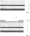
second dielectric layer 401 is formed onfluorocarbon layer 301, as shown inFIG. 4 . In one embodiment,second dielectric layer 401 may be a porous low-k dielectric layer or an ultra-low k dielectric layer. - Thereafter, an etch process is performed on second
dielectric layer 401 usingfluorocarbon layer 301 as an etch stop layer to form an opening extending to the surface offluorocarbon layer 301. - It is noted that, as employed herein, the term "opening," "via", or "trench" refers to an opening, a via, or a trench extending to a layer.
- In one embodiment, an opening extending to
fluorocarbon layer 301 may be formed by the steps shown inFIGS. 5 to 7 . - Referring to
FIG. 5 , a patternedhardmask layer 501 is formed on seconddielectric layer 401.Hardmask layer 501 has afirst opening 502 extending intohardmask layer 501. - In some embodiments, a
first hardmask layer 511, asecond hardmask layer 521, and athird hardmask layer 531 may be sequentially formed on seconddielectric layer 401. For example,first hardmask layer 511 may include non-porous SiOCH;second hardmask layer 521 may include tetraethyl orthosilicate (TEOS),third hardmask layer 531 may include titanium nitride (TiN). However, it is to be understood that the invention is not limited thereto. A patterned mask layer (e.g., a photoresist) is then formed overthird hardmask layer 531. In order to distinguish the patterned mask layer (not shown) from a first mask layer disclosed later, the patterned mask layer herein may be referred to as a second mask layer. An etch process is performed onthird hardmask layer 531 andsecond hardmask layer 521 using the second mask layer as a mask to form anopening 502 extending into second hardmask layer 521 (as shown inFIG. 5 ) or extending to the surface offirst hardmask layer 511. Preferably,first opening 502 may extend below the middle portion ofsecond hardmask layer 521 , that is, more than half of the thickness ofsecond hardmask layer 521 may be removed, as shown inFIG. 5 . Thereafter, the second mask layer is removed. That is,first opening 502 inhardmask layer 501 includes a remaining portion of second hardmask layer 521 (less than half of the thickness of second hardmask layer 521). - In some other embodiments, after
first hardmask layer 511,second hardmask layer 521, andthird hardmask layer 531 are sequentially formed, a mask oxide layer (e.g., silicon oxide) may be formed (not shown) onthird hardmask layer 531. The second mask layer is then formed on the mask oxide layer. Thereafter, the mask oxide layer,third hardmask layer 531, andsecond hardmask layer 521 are successively etched using the second mask layer as a mask to form the first opening. After removing the second mask layer, the remaining mask oxide layer is also removed. - Referring to
FIG. 6 , a patterned mask layer 601 (also referred to as a first mask layer), e.g., a photoresist, is formed onhard mask layer 501.First mask layer 601 has ansecond opening 602 extending to the bottom offirst opening 502. In one embodiment,second opening 602 may include two openings (as shown inFIG. 6 ), so that two through holes (vias) can be formed subsequently that extend tometal interconnect layer 201. In another embodiment,first mask layer 601 may havesecond opening 602 extending to the bottom offirst opening 501, so that a through hole (via) may be subsequently formed extending tometal interconnect layer 201. - Referring to
FIG. 7 , an etch process is performed onhardmask layer 501 and seconddielectric layer 401 usingfirst mask layer 601 as a mask.First mask layer 601 is then removed to form anopening 701 extending tofluorocarbon layer 301 and exposing a portion of the surface offluorocarbon layer 301. - The exposed portion of
fluorocarbon layer 301 and a portion of firstdielectric layer 202 under opening 701 may also be removed usinghardmask layer 501 as a mask to form anopening 801. A portion of thehardmask layer 501 in first opening 502 (i.e., the portion of the remaininghardmask layer 521, the portion offirst hardmask layer 511 below the remaininglayer 521 in the first opening), and a portion of seconddielectric layer 401 infirst opening 502 are also removed to form atrench 802 extending to the surface offluorocarbon layer 301, as shown inFIG. 8 . - In one embodiment, the exposed portion of
fluorocarbon layer 301 in opening 701 may be removed using a source gas of a first oxygen-containing plasma. In one embodiment, the portion of firstdielectric layer 202 under opening 701 may be etched using a source gas of a second CF4-containing plasma. In one embodiment, the source gas of the second plasma may also include CO or CO2. In addition, in the etching of the exposed portion offluorocarbon layer 301 and the portion of firstdielectric layer 202 below opening 701, nitrogen gas, argon gas, helium gas, or a combination thereof may be used as a carrier gas. - It is to be understood that the number of through holes extending to the metal interconnect layer can be any integer number N. In the example shown in
FIG. 8 , two throughholes 801 are shown extending fromfluorocarbon layer 301 tometal interconnect layer 201. But it is understood that the number is arbitrary chosen for describing the example embodiment and should not be limiting. In some other embodiments, as described above, the number of throughhole 801 may be one through hole. -
Fluorocarbon layer 301 enablestrench 802 in the different portions of the interconnect structure to have contact to the surface of the fluorocarbon layer, so that throughhole 801 in the different portions of the interconnect structure has contact to the surface of the fluorocarbon layer, thereby improving the uniformity oftrench 802 and throughhole 801 in the vertical direction (direction perpendicular to the surface of the metal interconnect layer). Metal interconnect lines that are formed by subsequently filling a metal layer in the trench and through hole(s) also have improved uniformity, which can reduce the parasitic capacitance between the metal interconnect lines. - Thereafter, a
metal layer 901 may be formed to filltrench 802 and throughhole 801, as shown inFIG. 9 .Metal layer 901 may also be formed on remaininghardmask layer 501. In one embodiment,metal layer 901 may include copper. - Thereafter, a planarization (e.g., a chemical mechanical polishing) process is performed on
metal layer 901 to form a metal interconnect line, as shown inFIG. 10 . In one embodiment, theplanarized metal layer 901 has a planar surface that is flush with the upper surface of seconddielectric layer 401. - Thus, a method for manufacturing an interconnect structure has been described above according to some embodiment of the present invention with reference to
FIGS. 2 through 10 . One of skill in the art will appreciate that steps shown inFIGS. 2 to 10 may be performed in different embodiments, and that some processes inFIGS. 2 to 10 are not necessary in one embodiment. - Embodiments of the present invention also provide a novel interconnect structure. Referring to
FIG. 8 , the interconnect structure may include ametal interconnect layer 201, a firstdielectric layer 202 onmetal interconnect layer 201, afluorocarbon layer 301 on firstdielectric layer 202, and asecond dielectric layer 401 onfluorocarbon layer 301.Second dielectric layer 401 includes atrench 802 extending to the surface offluorocarbon layer 301. The interconnect structure may also include a throughhole 801 intrench 801 extending throughfluorocarbon layer 301 and firstdielectric layer 202 to the surface ofmetal interconnect layer 201. In one embodiment, the interconnect structure may have two throughholes 801 in the trench that extend through the fluorocarbon layer and the first dielectric layer to the surface of metal interconnect layer. - In one embodiment, referring still to
FIG. 8 , the interconnect structure may further include afirst hardmask layer 511 on seconddielectric layer 401, asecond hardmask layer 521 onfirst hardmask layer 511, and athird hardmask layer 531 onsecond hardmask layer 521. In one exemplary embodiment,first hardmask layer 511 may include non-porous SiOCH;second hardmask layer 521 may include tetraethyl orthosilicate (TEOS),third hardmask layer 531 may include titanium nitride (TiN). - In one embodiment, referring to
FIG. 10 , the interconnect structure may further include ametal layer 901filling trench 802 and throughhole 801.Metal layer 901 may include copper. - Preferred embodiments of the present invention have been described in detail hereinabove.
- While the present invention is described herein with reference to illustrative embodiments, this description is not intended to be construed in a limiting sense. Rather, the purpose of the illustrative embodiments is to make the present invention be better understood by those skilled in the art. In order not to obscure the invention, many details of well-known processes and manufacturing techniques are omitted.
- Furthermore, some of the features of the preferred embodiments of the present invention could be used to advantage without the corresponding use of other features. As such, the foregoing description should be considered as merely illustrative of the principles of the invention, and not in limitation thereof.
Claims (15)
- A method for manufacturing an interconnect structure, the method comprising:providing a metal interconnect layer;forming a first dielectric layer on the metal interconnect layer;forming a fluorocarbon layer on the first dielectric layer;forming a second dielectric layer on the fluorocarbon layer;performing an etch process on the second dielectric layer using the fluorocarbon layer as an etch stop mask to form an opening.
- The method of claim 1, wherein performing the etch process comprises:forming a patterned hardmask layer on the second dielectric layer, the hardmask layer having a first opening extending into the hardmask layer;forming a patterned first mask layer on the hardmask layer, the first mask layer having a second opening extending to a bottom of the first opening;etching the hardmask layer and the second dielectric layer using the first mask layer as a mask to expose a portion of the fluorocarbon layer; andremoving the first mask layer to form the opening.
- The method of claim 2, further comprising:removing the exposed portion of the fluorocarbon layer and a portion of the first dielectric layer under the exposed portion of the fluorocarbon layer using the etched hardmask layer as a mask to form a through hole extending to the metal interconnect layer;removing a portion of the hardmask layer and a portion of the first dielectric layer below the first opening to form a trench extending to the fluorocarbon layer.
- The method of claim 3, wherein the second opening of the first mask layer comprises two openings extending to the bottom of the first opening to form two corresponding through holes extending to the metal interconnect layer.
- The method of claim 3 or 4, further comprising:forming a metal layer filling the trench and the through hole.
- The method of anyone of the claims 2-5, wherein forming the patterned hardmask layer on the second dielectric layer comprises:forming a first hardmask layer on the second dielectric layer, a second hardmask layer on the first hardmask layer, and a third hardmask layer on the second hardmask layer;forming a patterned second mask layer on the third hardmask layer;etching the third hardmask layer and the second hardmask layer using the second mask layer as a mask to form the opening extending into the second hardmask layer or extending into a surface off the first hardmask layer; andremoving the second mask layer.
- The method of claim 6, wherein forming the patterned second mask layer on the third hardmask layer comprises:forming a mask oxide layer on the third hardmask layer;forming the second mask layer on the mask oxide layer;etching the third hardmask layer and the second hardmask layer comprises:etching the mask oxide layer, the third hardmask layer, and the second hardmask layer using the second mask layer as a mask; and after removing the second mask layer, the method further comprising:removing a remaining portion of the mask oxide layer.
- The method of claim 6 or 7, wherein:the first hardmask layer comprises non-porous SiOCH;the second hardmask layer comprises tetraethyl orthosilicate (TEOS); andthe third hardmask layer comprises titanium nitride (TiN).
- The method of anyone of the claims 1-8, further comprising, after forming the fluorocarbon layer on the first dielectric layer:subjecting the fluorocarbon layer to an oxygen-containing plasma treatment; andwherein preferably: the oxygen-containing plasma treatment comprises a source gas including O2, O3, or H2O.
- The method of anyone of the claims 1-9, wherein
the first and second dielectric layers each comprise a porous low-k dielectric layer; and/or
the fluorocarbon layer is a hydrogen-containing fluorocarbon layer. - The method of anyone of the claims 1-10, wherein etching a portion of the fluorocarbon layer and a portion of the first dielectric layer below the opening using a remaining portion of the hardmask layer as a mask comprises:etching the portion of the fluorocarbon layer below the opening comprises a source gas including an O2 containing first plasma;etching the portion of the first dielectric layer below the opening comprises a source gas of a CF4 containing second plasma; andwherein preferably: the source gas of the second plasma further comprises CO or CO2.
- An interconnect structure comprising:a metal interconnect layer;a first dielectric layer on the metal interconnect layer;a fluorocarbon layer on the first dielectric layer;a second dielectric layer on the fluorocarbon layer;a trench extending through the second dielectric layer to the fluorocarbon layer; anda through hole in the trench extending to the metal interconnect layer.
- The interconnect structure of claim 12, wherein at least one of:the through hole comprises a first through hole and a second through hole;the first and second dielectric layers each comprise a porous low-k dielectric layer; andthe fluorocarbon layer is a hydrogen-containing fluorocarbon layer.
- The interconnect structure of claim 12 or 13, further comprising a metal layer filling the trench and the through hole.
- The interconnect structure of anyone of the claims 12-14, further comprising:a first hardmask layer comprising SiOCH on the second dielectric layer;a second hardmask layer comprising TEOS on the first hardmask layer; anda third hardmask layer comprising TiN on the second hardmask layer.
Applications Claiming Priority (1)
| Application Number | Priority Date | Filing Date | Title |
|---|---|---|---|
| CN201610868147.1A CN107887323B (en) | 2016-09-30 | 2016-09-30 | Interconnect structure and method of making the same |
Publications (2)
| Publication Number | Publication Date |
|---|---|
| EP3301705A1 true EP3301705A1 (en) | 2018-04-04 |
| EP3301705B1 EP3301705B1 (en) | 2019-06-19 |
Family
ID=59968969
Family Applications (1)
| Application Number | Title | Priority Date | Filing Date |
|---|---|---|---|
| EP17192406.1A Not-in-force EP3301705B1 (en) | 2016-09-30 | 2017-09-21 | Method for fluorocarbon film used as middle stop layer for porous low k film |
Country Status (3)
| Country | Link |
|---|---|
| US (2) | US10636672B2 (en) |
| EP (1) | EP3301705B1 (en) |
| CN (1) | CN107887323B (en) |
Cited By (2)
| Publication number | Priority date | Publication date | Assignee | Title |
|---|---|---|---|---|
| CN110838464A (en) * | 2018-08-16 | 2020-02-25 | 联华电子股份有限公司 | Metal interconnect structure and method of making the same |
| TWI849397B (en) * | 2021-09-08 | 2024-07-21 | 南韓商三星電子股份有限公司 | Method of fabricating semiconductor device including porous dielectric layer |
Families Citing this family (3)
| Publication number | Priority date | Publication date | Assignee | Title |
|---|---|---|---|---|
| CN109860041B (en) * | 2018-12-28 | 2020-12-29 | 芯创智(北京)微电子有限公司 | A kind of integrated circuit precision pattern preparation method |
| US12119226B2 (en) * | 2021-03-29 | 2024-10-15 | Changxin Memory Technologies, Inc. | Method for manufacturing mask structure, semiconductor structure and manufacturing method thereof |
| CN113223954B (en) * | 2021-04-25 | 2022-12-23 | 华虹半导体(无锡)有限公司 | A method for improving wafer burrs caused by trench etching |
Citations (4)
| Publication number | Priority date | Publication date | Assignee | Title |
|---|---|---|---|---|
| US5674355A (en) * | 1994-07-12 | 1997-10-07 | International Business Machines Corp. | Diamond-like carbon for use in VLSI and ULSI interconnect systems |
| US6291334B1 (en) * | 1997-12-19 | 2001-09-18 | Applied Materials, Inc. | Etch stop layer for dual damascene process |
| US20020054962A1 (en) * | 1999-06-18 | 2002-05-09 | Judy Huang | Plasma treatment to enhance adhesion and to minimize oxidation of carbon-containing layers |
| US20150262912A1 (en) * | 2014-03-14 | 2015-09-17 | Taiwan Semiconductor Manufacturing Company, Ltd. | Via Corner Engineering in Trench-First Dual Damascene Process |
Family Cites Families (9)
| Publication number | Priority date | Publication date | Assignee | Title |
|---|---|---|---|---|
| US6949203B2 (en) | 1999-12-28 | 2005-09-27 | Applied Materials, Inc. | System level in-situ integrated dielectric etch process particularly useful for copper dual damascene |
| US6696365B2 (en) * | 2002-01-07 | 2004-02-24 | Applied Materials, Inc. | Process for in-situ etching a hardmask stack |
| US20030190829A1 (en) | 2002-04-05 | 2003-10-09 | Brennan Kenneth D. | Dual damascene barrier structures and preferential etching method |
| JP4668522B2 (en) * | 2003-03-31 | 2011-04-13 | 東京エレクトロン株式会社 | Plasma processing method |
| US7432210B2 (en) * | 2005-10-05 | 2008-10-07 | Applied Materials, Inc. | Process to open carbon based hardmask |
| JP5143769B2 (en) | 2008-03-12 | 2013-02-13 | 東京エレクトロン株式会社 | Semiconductor device and manufacturing method thereof |
| US20100022091A1 (en) * | 2008-07-25 | 2010-01-28 | Li Siyi | Method for plasma etching porous low-k dielectric layers |
| US20140054754A1 (en) * | 2012-08-21 | 2014-02-27 | Toshiba America Electronic Components, Inc. | Optically reactive masking |
| TWM485462U (en) * | 2014-05-02 | 2014-09-01 | Qin He Information Co Ltd | Community service integration platform |
-
2016
- 2016-09-30 CN CN201610868147.1A patent/CN107887323B/en active Active
-
2017
- 2017-07-31 US US15/664,966 patent/US10636672B2/en active Active
- 2017-09-21 EP EP17192406.1A patent/EP3301705B1/en not_active Not-in-force
-
2020
- 2020-03-26 US US16/831,336 patent/US20200227272A1/en not_active Abandoned
Patent Citations (4)
| Publication number | Priority date | Publication date | Assignee | Title |
|---|---|---|---|---|
| US5674355A (en) * | 1994-07-12 | 1997-10-07 | International Business Machines Corp. | Diamond-like carbon for use in VLSI and ULSI interconnect systems |
| US6291334B1 (en) * | 1997-12-19 | 2001-09-18 | Applied Materials, Inc. | Etch stop layer for dual damascene process |
| US20020054962A1 (en) * | 1999-06-18 | 2002-05-09 | Judy Huang | Plasma treatment to enhance adhesion and to minimize oxidation of carbon-containing layers |
| US20150262912A1 (en) * | 2014-03-14 | 2015-09-17 | Taiwan Semiconductor Manufacturing Company, Ltd. | Via Corner Engineering in Trench-First Dual Damascene Process |
Cited By (4)
| Publication number | Priority date | Publication date | Assignee | Title |
|---|---|---|---|---|
| CN110838464A (en) * | 2018-08-16 | 2020-02-25 | 联华电子股份有限公司 | Metal interconnect structure and method of making the same |
| CN110838464B (en) * | 2018-08-16 | 2023-04-25 | 联华电子股份有限公司 | Metal interconnection structure and manufacturing method thereof |
| TWI849397B (en) * | 2021-09-08 | 2024-07-21 | 南韓商三星電子股份有限公司 | Method of fabricating semiconductor device including porous dielectric layer |
| US12308245B2 (en) | 2021-09-08 | 2025-05-20 | Samsung Electronics Co., Ltd. | Method of fabricating semiconductor device including porous dielectric layer |
Also Published As
| Publication number | Publication date |
|---|---|
| CN107887323B (en) | 2020-06-05 |
| US20180096857A1 (en) | 2018-04-05 |
| CN107887323A (en) | 2018-04-06 |
| US20200227272A1 (en) | 2020-07-16 |
| US10636672B2 (en) | 2020-04-28 |
| EP3301705B1 (en) | 2019-06-19 |
Similar Documents
| Publication | Publication Date | Title |
|---|---|---|
| US20200227272A1 (en) | Interconnect Structure with Porous Low K Film | |
| US7767587B2 (en) | Method of forming an interconnection structure in a organosilicate glass having a porous layer with higher carbon content located between two lower carbon content non-porous layers | |
| US20090200636A1 (en) | Sub-lithographic dimensioned air gap formation and related structure | |
| US9293363B2 (en) | Methods and structures for back end of line integration | |
| US9412651B2 (en) | Air-gap formation in interconnect structures | |
| US7015133B2 (en) | Dual damascene structure formed of low-k dielectric materials | |
| US11217458B2 (en) | Method for forming semiconductor device structure with fine line pitch and fine end-to-end space | |
| EP3264458A1 (en) | Method for capping cu layer using graphene in semiconductor | |
| US8728936B1 (en) | Copper etching integration scheme | |
| KR102733881B1 (en) | Semiconductor device having an interconnection structure | |
| TWI899421B (en) | Method of forming semiconductor device and interconnect structure | |
| US6774031B2 (en) | Method of forming dual-damascene structure | |
| CN104851835A (en) | Metal interconnection structure and forming method thereof | |
| US6524962B2 (en) | Method for forming dual-damascene interconnect structure | |
| US8084357B2 (en) | Method for manufacturing a dual damascene opening comprising a trench opening and a via opening | |
| KR20040101008A (en) | Manufacturing method for semiconductor apparatus | |
| US11081478B2 (en) | Interconnect structure having a fluorocarbon layer | |
| KR20230085819A (en) | Film deposition for patterning process | |
| US20080057727A1 (en) | Method of manufacturing a semiconductor device | |
| KR101024871B1 (en) | How to form a dual damascene pattern | |
| JP2006108336A (en) | Manufacturing method of semiconductor device | |
| JPH11176935A (en) | Method for manufacturing semiconductor device | |
| CN111933580A (en) | Preparation method of semiconductor structure | |
| KR20010030169A (en) | Reduced Capacitance Dielectric Structure For Integrated Circuits |
Legal Events
| Date | Code | Title | Description |
|---|---|---|---|
| PUAI | Public reference made under article 153(3) epc to a published international application that has entered the european phase |
Free format text: ORIGINAL CODE: 0009012 |
|
| STAA | Information on the status of an ep patent application or granted ep patent |
Free format text: STATUS: THE APPLICATION HAS BEEN PUBLISHED |
|
| AK | Designated contracting states |
Kind code of ref document: A1 Designated state(s): AL AT BE BG CH CY CZ DE DK EE ES FI FR GB GR HR HU IE IS IT LI LT LU LV MC MK MT NL NO PL PT RO RS SE SI SK SM TR |
|
| AX | Request for extension of the european patent |
Extension state: BA ME |
|
| STAA | Information on the status of an ep patent application or granted ep patent |
Free format text: STATUS: REQUEST FOR EXAMINATION WAS MADE |
|
| 17P | Request for examination filed |
Effective date: 20180918 |
|
| RBV | Designated contracting states (corrected) |
Designated state(s): AL AT BE BG CH CY CZ DE DK EE ES FI FR GB GR HR HU IE IS IT LI LT LU LV MC MK MT NL NO PL PT RO RS SE SI SK SM TR |
|
| RAP1 | Party data changed (applicant data changed or rights of an application transferred) |
Owner name: SEMICONDUCTOR MANUFACTURING INTERNATIONAL (BEIJING Owner name: SEMICONDUCTOR MANUFACTURING INTERNATIONAL (SHANGHA |
|
| GRAP | Despatch of communication of intention to grant a patent |
Free format text: ORIGINAL CODE: EPIDOSNIGR1 |
|
| STAA | Information on the status of an ep patent application or granted ep patent |
Free format text: STATUS: GRANT OF PATENT IS INTENDED |
|
| RIC1 | Information provided on ipc code assigned before grant |
Ipc: H01L 23/532 20060101ALI20181212BHEP Ipc: H01L 21/312 20060101ALN20181212BHEP Ipc: H01L 21/311 20060101AFI20181212BHEP Ipc: H01L 21/768 20060101ALI20181212BHEP |
|
| INTG | Intention to grant announced |
Effective date: 20190108 |
|
| GRAS | Grant fee paid |
Free format text: ORIGINAL CODE: EPIDOSNIGR3 |
|
| GRAA | (expected) grant |
Free format text: ORIGINAL CODE: 0009210 |
|
| STAA | Information on the status of an ep patent application or granted ep patent |
Free format text: STATUS: THE PATENT HAS BEEN GRANTED |
|
| AK | Designated contracting states |
Kind code of ref document: B1 Designated state(s): AL AT BE BG CH CY CZ DE DK EE ES FI FR GB GR HR HU IE IS IT LI LT LU LV MC MK MT NL NO PL PT RO RS SE SI SK SM TR |
|
| REG | Reference to a national code |
Ref country code: GB Ref legal event code: FG4D |
|
| REG | Reference to a national code |
Ref country code: CH Ref legal event code: EP |
|
| REG | Reference to a national code |
Ref country code: IE Ref legal event code: FG4D |
|
| REG | Reference to a national code |
Ref country code: DE Ref legal event code: R096 Ref document number: 602017004634 Country of ref document: DE |
|
| REG | Reference to a national code |
Ref country code: AT Ref legal event code: REF Ref document number: 1146569 Country of ref document: AT Kind code of ref document: T Effective date: 20190715 |
|
| REG | Reference to a national code |
Ref country code: NL Ref legal event code: MP Effective date: 20190619 |
|
| PG25 | Lapsed in a contracting state [announced via postgrant information from national office to epo] |
Ref country code: AL Free format text: LAPSE BECAUSE OF FAILURE TO SUBMIT A TRANSLATION OF THE DESCRIPTION OR TO PAY THE FEE WITHIN THE PRESCRIBED TIME-LIMIT Effective date: 20190619 Ref country code: SE Free format text: LAPSE BECAUSE OF FAILURE TO SUBMIT A TRANSLATION OF THE DESCRIPTION OR TO PAY THE FEE WITHIN THE PRESCRIBED TIME-LIMIT Effective date: 20190619 Ref country code: NO Free format text: LAPSE BECAUSE OF FAILURE TO SUBMIT A TRANSLATION OF THE DESCRIPTION OR TO PAY THE FEE WITHIN THE PRESCRIBED TIME-LIMIT Effective date: 20190919 Ref country code: HR Free format text: LAPSE BECAUSE OF FAILURE TO SUBMIT A TRANSLATION OF THE DESCRIPTION OR TO PAY THE FEE WITHIN THE PRESCRIBED TIME-LIMIT Effective date: 20190619 Ref country code: LT Free format text: LAPSE BECAUSE OF FAILURE TO SUBMIT A TRANSLATION OF THE DESCRIPTION OR TO PAY THE FEE WITHIN THE PRESCRIBED TIME-LIMIT Effective date: 20190619 Ref country code: FI Free format text: LAPSE BECAUSE OF FAILURE TO SUBMIT A TRANSLATION OF THE DESCRIPTION OR TO PAY THE FEE WITHIN THE PRESCRIBED TIME-LIMIT Effective date: 20190619 |
|
| REG | Reference to a national code |
Ref country code: LT Ref legal event code: MG4D |
|
| PG25 | Lapsed in a contracting state [announced via postgrant information from national office to epo] |
Ref country code: LV Free format text: LAPSE BECAUSE OF FAILURE TO SUBMIT A TRANSLATION OF THE DESCRIPTION OR TO PAY THE FEE WITHIN THE PRESCRIBED TIME-LIMIT Effective date: 20190619 Ref country code: GR Free format text: LAPSE BECAUSE OF FAILURE TO SUBMIT A TRANSLATION OF THE DESCRIPTION OR TO PAY THE FEE WITHIN THE PRESCRIBED TIME-LIMIT Effective date: 20190920 Ref country code: RS Free format text: LAPSE BECAUSE OF FAILURE TO SUBMIT A TRANSLATION OF THE DESCRIPTION OR TO PAY THE FEE WITHIN THE PRESCRIBED TIME-LIMIT Effective date: 20190619 Ref country code: BG Free format text: LAPSE BECAUSE OF FAILURE TO SUBMIT A TRANSLATION OF THE DESCRIPTION OR TO PAY THE FEE WITHIN THE PRESCRIBED TIME-LIMIT Effective date: 20190919 |
|
| REG | Reference to a national code |
Ref country code: AT Ref legal event code: MK05 Ref document number: 1146569 Country of ref document: AT Kind code of ref document: T Effective date: 20190619 |
|
| PG25 | Lapsed in a contracting state [announced via postgrant information from national office to epo] |
Ref country code: SK Free format text: LAPSE BECAUSE OF FAILURE TO SUBMIT A TRANSLATION OF THE DESCRIPTION OR TO PAY THE FEE WITHIN THE PRESCRIBED TIME-LIMIT Effective date: 20190619 Ref country code: EE Free format text: LAPSE BECAUSE OF FAILURE TO SUBMIT A TRANSLATION OF THE DESCRIPTION OR TO PAY THE FEE WITHIN THE PRESCRIBED TIME-LIMIT Effective date: 20190619 Ref country code: PT Free format text: LAPSE BECAUSE OF FAILURE TO SUBMIT A TRANSLATION OF THE DESCRIPTION OR TO PAY THE FEE WITHIN THE PRESCRIBED TIME-LIMIT Effective date: 20191021 Ref country code: AT Free format text: LAPSE BECAUSE OF FAILURE TO SUBMIT A TRANSLATION OF THE DESCRIPTION OR TO PAY THE FEE WITHIN THE PRESCRIBED TIME-LIMIT Effective date: 20190619 Ref country code: CZ Free format text: LAPSE BECAUSE OF FAILURE TO SUBMIT A TRANSLATION OF THE DESCRIPTION OR TO PAY THE FEE WITHIN THE PRESCRIBED TIME-LIMIT Effective date: 20190619 Ref country code: NL Free format text: LAPSE BECAUSE OF FAILURE TO SUBMIT A TRANSLATION OF THE DESCRIPTION OR TO PAY THE FEE WITHIN THE PRESCRIBED TIME-LIMIT Effective date: 20190619 Ref country code: RO Free format text: LAPSE BECAUSE OF FAILURE TO SUBMIT A TRANSLATION OF THE DESCRIPTION OR TO PAY THE FEE WITHIN THE PRESCRIBED TIME-LIMIT Effective date: 20190619 |
|
| PG25 | Lapsed in a contracting state [announced via postgrant information from national office to epo] |
Ref country code: ES Free format text: LAPSE BECAUSE OF FAILURE TO SUBMIT A TRANSLATION OF THE DESCRIPTION OR TO PAY THE FEE WITHIN THE PRESCRIBED TIME-LIMIT Effective date: 20190619 Ref country code: SM Free format text: LAPSE BECAUSE OF FAILURE TO SUBMIT A TRANSLATION OF THE DESCRIPTION OR TO PAY THE FEE WITHIN THE PRESCRIBED TIME-LIMIT Effective date: 20190619 Ref country code: IT Free format text: LAPSE BECAUSE OF FAILURE TO SUBMIT A TRANSLATION OF THE DESCRIPTION OR TO PAY THE FEE WITHIN THE PRESCRIBED TIME-LIMIT Effective date: 20190619 Ref country code: IS Free format text: LAPSE BECAUSE OF FAILURE TO SUBMIT A TRANSLATION OF THE DESCRIPTION OR TO PAY THE FEE WITHIN THE PRESCRIBED TIME-LIMIT Effective date: 20191019 |
|
| PG25 | Lapsed in a contracting state [announced via postgrant information from national office to epo] |
Ref country code: TR Free format text: LAPSE BECAUSE OF FAILURE TO SUBMIT A TRANSLATION OF THE DESCRIPTION OR TO PAY THE FEE WITHIN THE PRESCRIBED TIME-LIMIT Effective date: 20190619 |
|
| REG | Reference to a national code |
Ref country code: DE Ref legal event code: R119 Ref document number: 602017004634 Country of ref document: DE |
|
| PG25 | Lapsed in a contracting state [announced via postgrant information from national office to epo] |
Ref country code: PL Free format text: LAPSE BECAUSE OF FAILURE TO SUBMIT A TRANSLATION OF THE DESCRIPTION OR TO PAY THE FEE WITHIN THE PRESCRIBED TIME-LIMIT Effective date: 20190619 Ref country code: DK Free format text: LAPSE BECAUSE OF FAILURE TO SUBMIT A TRANSLATION OF THE DESCRIPTION OR TO PAY THE FEE WITHIN THE PRESCRIBED TIME-LIMIT Effective date: 20190619 |
|
| PG25 | Lapsed in a contracting state [announced via postgrant information from national office to epo] |
Ref country code: MC Free format text: LAPSE BECAUSE OF FAILURE TO SUBMIT A TRANSLATION OF THE DESCRIPTION OR TO PAY THE FEE WITHIN THE PRESCRIBED TIME-LIMIT Effective date: 20190619 Ref country code: IS Free format text: LAPSE BECAUSE OF FAILURE TO SUBMIT A TRANSLATION OF THE DESCRIPTION OR TO PAY THE FEE WITHIN THE PRESCRIBED TIME-LIMIT Effective date: 20200224 |
|
| PLBE | No opposition filed within time limit |
Free format text: ORIGINAL CODE: 0009261 |
|
| STAA | Information on the status of an ep patent application or granted ep patent |
Free format text: STATUS: NO OPPOSITION FILED WITHIN TIME LIMIT |
|
| PG2D | Information on lapse in contracting state deleted |
Ref country code: IS |
|
| PG25 | Lapsed in a contracting state [announced via postgrant information from national office to epo] |
Ref country code: LU Free format text: LAPSE BECAUSE OF NON-PAYMENT OF DUE FEES Effective date: 20190921 Ref country code: IE Free format text: LAPSE BECAUSE OF NON-PAYMENT OF DUE FEES Effective date: 20190921 Ref country code: DE Free format text: LAPSE BECAUSE OF NON-PAYMENT OF DUE FEES Effective date: 20200401 |
|
| REG | Reference to a national code |
Ref country code: BE Ref legal event code: MM Effective date: 20190930 |
|
| 26N | No opposition filed |
Effective date: 20200603 |
|
| PG25 | Lapsed in a contracting state [announced via postgrant information from national office to epo] |
Ref country code: SI Free format text: LAPSE BECAUSE OF FAILURE TO SUBMIT A TRANSLATION OF THE DESCRIPTION OR TO PAY THE FEE WITHIN THE PRESCRIBED TIME-LIMIT Effective date: 20190619 Ref country code: BE Free format text: LAPSE BECAUSE OF NON-PAYMENT OF DUE FEES Effective date: 20190930 |
|
| PG25 | Lapsed in a contracting state [announced via postgrant information from national office to epo] |
Ref country code: FR Free format text: LAPSE BECAUSE OF NON-PAYMENT OF DUE FEES Effective date: 20190930 |
|
| REG | Reference to a national code |
Ref country code: CH Ref legal event code: PL |
|
| PG25 | Lapsed in a contracting state [announced via postgrant information from national office to epo] |
Ref country code: CY Free format text: LAPSE BECAUSE OF FAILURE TO SUBMIT A TRANSLATION OF THE DESCRIPTION OR TO PAY THE FEE WITHIN THE PRESCRIBED TIME-LIMIT Effective date: 20190619 |
|
| PG25 | Lapsed in a contracting state [announced via postgrant information from national office to epo] |
Ref country code: HU Free format text: LAPSE BECAUSE OF FAILURE TO SUBMIT A TRANSLATION OF THE DESCRIPTION OR TO PAY THE FEE WITHIN THE PRESCRIBED TIME-LIMIT; INVALID AB INITIO Effective date: 20170921 Ref country code: MT Free format text: LAPSE BECAUSE OF FAILURE TO SUBMIT A TRANSLATION OF THE DESCRIPTION OR TO PAY THE FEE WITHIN THE PRESCRIBED TIME-LIMIT Effective date: 20190619 |
|
| PG25 | Lapsed in a contracting state [announced via postgrant information from national office to epo] |
Ref country code: CH Free format text: LAPSE BECAUSE OF NON-PAYMENT OF DUE FEES Effective date: 20200930 Ref country code: LI Free format text: LAPSE BECAUSE OF NON-PAYMENT OF DUE FEES Effective date: 20200930 |
|
| GBPC | Gb: european patent ceased through non-payment of renewal fee |
Effective date: 20210921 |
|
| PG25 | Lapsed in a contracting state [announced via postgrant information from national office to epo] |
Ref country code: MK Free format text: LAPSE BECAUSE OF FAILURE TO SUBMIT A TRANSLATION OF THE DESCRIPTION OR TO PAY THE FEE WITHIN THE PRESCRIBED TIME-LIMIT Effective date: 20190619 |
|
| PG25 | Lapsed in a contracting state [announced via postgrant information from national office to epo] |
Ref country code: GB Free format text: LAPSE BECAUSE OF NON-PAYMENT OF DUE FEES Effective date: 20210921 |