EP3301703A1 - Semiconductor device and manufacturing method thereof - Google Patents
Semiconductor device and manufacturing method thereof Download PDFInfo
- Publication number
- EP3301703A1 EP3301703A1 EP17188984.3A EP17188984A EP3301703A1 EP 3301703 A1 EP3301703 A1 EP 3301703A1 EP 17188984 A EP17188984 A EP 17188984A EP 3301703 A1 EP3301703 A1 EP 3301703A1
- Authority
- EP
- European Patent Office
- Prior art keywords
- dielectric layer
- layer
- substrate
- recesses
- graphene
- Prior art date
- Legal status (The legal status is an assumption and is not a legal conclusion. Google has not performed a legal analysis and makes no representation as to the accuracy of the status listed.)
- Withdrawn
Links
Images


Classifications
-
- H—ELECTRICITY
- H10—SEMICONDUCTOR DEVICES; ELECTRIC SOLID-STATE DEVICES NOT OTHERWISE PROVIDED FOR
- H10D—INORGANIC ELECTRIC SEMICONDUCTOR DEVICES
- H10D62/00—Semiconductor bodies, or regions thereof, of devices having potential barriers
- H10D62/80—Semiconductor bodies, or regions thereof, of devices having potential barriers characterised by the materials
- H10D62/83—Semiconductor bodies, or regions thereof, of devices having potential barriers characterised by the materials being Group IV materials, e.g. B-doped Si or undoped Ge
- H10D62/8303—Diamond
-
- H—ELECTRICITY
- H10—SEMICONDUCTOR DEVICES; ELECTRIC SOLID-STATE DEVICES NOT OTHERWISE PROVIDED FOR
- H10B—ELECTRONIC MEMORY DEVICES
- H10B10/00—Static random access memory [SRAM] devices
- H10B10/12—Static random access memory [SRAM] devices comprising a MOSFET load element
- H10B10/125—Static random access memory [SRAM] devices comprising a MOSFET load element the MOSFET being a thin film transistor [TFT]
-
- H—ELECTRICITY
- H10—SEMICONDUCTOR DEVICES; ELECTRIC SOLID-STATE DEVICES NOT OTHERWISE PROVIDED FOR
- H10D—INORGANIC ELECTRIC SEMICONDUCTOR DEVICES
- H10D30/00—Field-effect transistors [FET]
- H10D30/01—Manufacture or treatment
- H10D30/021—Manufacture or treatment of FETs having insulated gates [IGFET]
- H10D30/024—Manufacture or treatment of FETs having insulated gates [IGFET] of fin field-effect transistors [FinFET]
-
- H—ELECTRICITY
- H10—SEMICONDUCTOR DEVICES; ELECTRIC SOLID-STATE DEVICES NOT OTHERWISE PROVIDED FOR
- H10D—INORGANIC ELECTRIC SEMICONDUCTOR DEVICES
- H10D30/00—Field-effect transistors [FET]
- H10D30/01—Manufacture or treatment
- H10D30/021—Manufacture or treatment of FETs having insulated gates [IGFET]
- H10D30/026—Manufacture or treatment of FETs having insulated gates [IGFET] having laterally-coplanar source and drain regions, a gate at the sides of the bulk channel, and both horizontal and vertical current flow
-
- H—ELECTRICITY
- H10—SEMICONDUCTOR DEVICES; ELECTRIC SOLID-STATE DEVICES NOT OTHERWISE PROVIDED FOR
- H10D—INORGANIC ELECTRIC SEMICONDUCTOR DEVICES
- H10D30/00—Field-effect transistors [FET]
- H10D30/40—FETs having zero-dimensional [0D], one-dimensional [1D] or two-dimensional [2D] charge carrier gas channels
- H10D30/47—FETs having zero-dimensional [0D], one-dimensional [1D] or two-dimensional [2D] charge carrier gas channels having two-dimensional [2D] charge carrier gas channels, e.g. nanoribbon FETs or high electron mobility transistors [HEMT]
-
- H—ELECTRICITY
- H10—SEMICONDUCTOR DEVICES; ELECTRIC SOLID-STATE DEVICES NOT OTHERWISE PROVIDED FOR
- H10D—INORGANIC ELECTRIC SEMICONDUCTOR DEVICES
- H10D30/00—Field-effect transistors [FET]
- H10D30/60—Insulated-gate field-effect transistors [IGFET]
- H10D30/62—Fin field-effect transistors [FinFET]
-
- H—ELECTRICITY
- H10—SEMICONDUCTOR DEVICES; ELECTRIC SOLID-STATE DEVICES NOT OTHERWISE PROVIDED FOR
- H10D—INORGANIC ELECTRIC SEMICONDUCTOR DEVICES
- H10D30/00—Field-effect transistors [FET]
- H10D30/60—Insulated-gate field-effect transistors [IGFET]
- H10D30/67—Thin-film transistors [TFT]
- H10D30/674—Thin-film transistors [TFT] characterised by the active materials
- H10D30/6741—Group IV materials, e.g. germanium or silicon carbide
-
- H—ELECTRICITY
- H10—SEMICONDUCTOR DEVICES; ELECTRIC SOLID-STATE DEVICES NOT OTHERWISE PROVIDED FOR
- H10D—INORGANIC ELECTRIC SEMICONDUCTOR DEVICES
- H10D30/00—Field-effect transistors [FET]
- H10D30/60—Insulated-gate field-effect transistors [IGFET]
- H10D30/67—Thin-film transistors [TFT]
- H10D30/6758—Thin-film transistors [TFT] characterised by the insulating substrates
-
- H—ELECTRICITY
- H10—SEMICONDUCTOR DEVICES; ELECTRIC SOLID-STATE DEVICES NOT OTHERWISE PROVIDED FOR
- H10D—INORGANIC ELECTRIC SEMICONDUCTOR DEVICES
- H10D62/00—Semiconductor bodies, or regions thereof, of devices having potential barriers
- H10D62/10—Shapes, relative sizes or dispositions of the regions of the semiconductor bodies; Shapes of the semiconductor bodies
- H10D62/17—Semiconductor regions connected to electrodes not carrying current to be rectified, amplified or switched, e.g. channel regions
- H10D62/213—Channel regions of field-effect devices
- H10D62/221—Channel regions of field-effect devices of FETs
- H10D62/235—Channel regions of field-effect devices of FETs of IGFETs
- H10D62/292—Non-planar channels of IGFETs
-
- H—ELECTRICITY
- H10—SEMICONDUCTOR DEVICES; ELECTRIC SOLID-STATE DEVICES NOT OTHERWISE PROVIDED FOR
- H10D—INORGANIC ELECTRIC SEMICONDUCTOR DEVICES
- H10D62/00—Semiconductor bodies, or regions thereof, of devices having potential barriers
- H10D62/80—Semiconductor bodies, or regions thereof, of devices having potential barriers characterised by the materials
- H10D62/881—Semiconductor bodies, or regions thereof, of devices having potential barriers characterised by the materials being a two-dimensional material
- H10D62/882—Graphene
-
- H—ELECTRICITY
- H10—SEMICONDUCTOR DEVICES; ELECTRIC SOLID-STATE DEVICES NOT OTHERWISE PROVIDED FOR
- H10D—INORGANIC ELECTRIC SEMICONDUCTOR DEVICES
- H10D84/00—Integrated devices formed in or on semiconductor substrates that comprise only semiconducting layers, e.g. on Si wafers or on GaAs-on-Si wafers
- H10D84/01—Manufacture or treatment
- H10D84/0123—Integrating together multiple components covered by H10D12/00 or H10D30/00, e.g. integrating multiple IGBTs
- H10D84/0126—Integrating together multiple components covered by H10D12/00 or H10D30/00, e.g. integrating multiple IGBTs the components including insulated gates, e.g. IGFETs
- H10D84/0158—Integrating together multiple components covered by H10D12/00 or H10D30/00, e.g. integrating multiple IGBTs the components including insulated gates, e.g. IGFETs the components including FinFETs
-
- H—ELECTRICITY
- H10—SEMICONDUCTOR DEVICES; ELECTRIC SOLID-STATE DEVICES NOT OTHERWISE PROVIDED FOR
- H10D—INORGANIC ELECTRIC SEMICONDUCTOR DEVICES
- H10D84/00—Integrated devices formed in or on semiconductor substrates that comprise only semiconducting layers, e.g. on Si wafers or on GaAs-on-Si wafers
- H10D84/01—Manufacture or treatment
- H10D84/02—Manufacture or treatment characterised by using material-based technologies
- H10D84/03—Manufacture or treatment characterised by using material-based technologies using Group IV technology, e.g. silicon technology or silicon-carbide [SiC] technology
- H10D84/038—Manufacture or treatment characterised by using material-based technologies using Group IV technology, e.g. silicon technology or silicon-carbide [SiC] technology using silicon technology, e.g. SiGe
-
- H—ELECTRICITY
- H10—SEMICONDUCTOR DEVICES; ELECTRIC SOLID-STATE DEVICES NOT OTHERWISE PROVIDED FOR
- H10D—INORGANIC ELECTRIC SEMICONDUCTOR DEVICES
- H10D86/00—Integrated devices formed in or on insulating or conducting substrates, e.g. formed in silicon-on-insulator [SOI] substrates or on stainless steel or glass substrates
- H10D86/201—Integrated devices formed in or on insulating or conducting substrates, e.g. formed in silicon-on-insulator [SOI] substrates or on stainless steel or glass substrates the substrates comprising an insulating layer on a semiconductor body, e.g. SOI
-
- H—ELECTRICITY
- H10—SEMICONDUCTOR DEVICES; ELECTRIC SOLID-STATE DEVICES NOT OTHERWISE PROVIDED FOR
- H10P—GENERIC PROCESSES OR APPARATUS FOR THE MANUFACTURE OR TREATMENT OF DEVICES COVERED BY CLASS H10
- H10P14/00—Formation of materials, e.g. in the shape of layers or pillars
- H10P14/20—Formation of materials, e.g. in the shape of layers or pillars of semiconductor materials
- H10P14/24—Formation of materials, e.g. in the shape of layers or pillars of semiconductor materials using chemical vapour deposition [CVD]
-
- H—ELECTRICITY
- H10—SEMICONDUCTOR DEVICES; ELECTRIC SOLID-STATE DEVICES NOT OTHERWISE PROVIDED FOR
- H10P—GENERIC PROCESSES OR APPARATUS FOR THE MANUFACTURE OR TREATMENT OF DEVICES COVERED BY CLASS H10
- H10P14/00—Formation of materials, e.g. in the shape of layers or pillars
- H10P14/20—Formation of materials, e.g. in the shape of layers or pillars of semiconductor materials
- H10P14/27—Formation of materials, e.g. in the shape of layers or pillars of semiconductor materials using selective deposition, e.g. simultaneous growth of monocrystalline and non-monocrystalline semiconductor materials
- H10P14/271—Formation of materials, e.g. in the shape of layers or pillars of semiconductor materials using selective deposition, e.g. simultaneous growth of monocrystalline and non-monocrystalline semiconductor materials characterised by the preparation of substrate for selective deposition
-
- H—ELECTRICITY
- H10—SEMICONDUCTOR DEVICES; ELECTRIC SOLID-STATE DEVICES NOT OTHERWISE PROVIDED FOR
- H10P—GENERIC PROCESSES OR APPARATUS FOR THE MANUFACTURE OR TREATMENT OF DEVICES COVERED BY CLASS H10
- H10P14/00—Formation of materials, e.g. in the shape of layers or pillars
- H10P14/20—Formation of materials, e.g. in the shape of layers or pillars of semiconductor materials
- H10P14/32—Formation of materials, e.g. in the shape of layers or pillars of semiconductor materials characterised by intermediate layers between substrates and deposited layers
- H10P14/3202—Materials thereof
- H10P14/3238—Materials thereof being insulating materials
-
- H—ELECTRICITY
- H10—SEMICONDUCTOR DEVICES; ELECTRIC SOLID-STATE DEVICES NOT OTHERWISE PROVIDED FOR
- H10P—GENERIC PROCESSES OR APPARATUS FOR THE MANUFACTURE OR TREATMENT OF DEVICES COVERED BY CLASS H10
- H10P14/00—Formation of materials, e.g. in the shape of layers or pillars
- H10P14/20—Formation of materials, e.g. in the shape of layers or pillars of semiconductor materials
- H10P14/34—Deposited materials, e.g. layers
- H10P14/3402—Deposited materials, e.g. layers characterised by the chemical composition
- H10P14/3404—Deposited materials, e.g. layers characterised by the chemical composition being Group IVA materials
- H10P14/3406—Carbon, e.g. diamond-like carbon
-
- H—ELECTRICITY
- H10—SEMICONDUCTOR DEVICES; ELECTRIC SOLID-STATE DEVICES NOT OTHERWISE PROVIDED FOR
- H10W—GENERIC PACKAGES, INTERCONNECTIONS, CONNECTORS OR OTHER CONSTRUCTIONAL DETAILS OF DEVICES COVERED BY CLASS H10
- H10W20/00—Interconnections in chips, wafers or substrates
- H10W20/01—Manufacture or treatment
- H10W20/031—Manufacture or treatment of conductive parts of the interconnections
- H10W20/032—Manufacture or treatment of conductive parts of the interconnections of conductive barrier, adhesion or liner layers
- H10W20/052—Manufacture or treatment of conductive parts of the interconnections of conductive barrier, adhesion or liner layers by treatments not introducing additional elements therein
-
- H—ELECTRICITY
- H10—SEMICONDUCTOR DEVICES; ELECTRIC SOLID-STATE DEVICES NOT OTHERWISE PROVIDED FOR
- H10N—ELECTRIC SOLID-STATE DEVICES NOT OTHERWISE PROVIDED FOR
- H10N70/00—Solid-state devices having no potential barriers, and specially adapted for rectifying, amplifying, oscillating or switching
- H10N70/20—Multistable switching devices, e.g. memristors
- H10N70/231—Multistable switching devices, e.g. memristors based on solid-state phase change, e.g. between amorphous and crystalline phases, Ovshinsky effect
-
- H—ELECTRICITY
- H10—SEMICONDUCTOR DEVICES; ELECTRIC SOLID-STATE DEVICES NOT OTHERWISE PROVIDED FOR
- H10P—GENERIC PROCESSES OR APPARATUS FOR THE MANUFACTURE OR TREATMENT OF DEVICES COVERED BY CLASS H10
- H10P14/00—Formation of materials, e.g. in the shape of layers or pillars
- H10P14/20—Formation of materials, e.g. in the shape of layers or pillars of semiconductor materials
- H10P14/38—Formation of materials, e.g. in the shape of layers or pillars of semiconductor materials characterised by treatments done after the formation of the materials
-
- H—ELECTRICITY
- H10—SEMICONDUCTOR DEVICES; ELECTRIC SOLID-STATE DEVICES NOT OTHERWISE PROVIDED FOR
- H10P—GENERIC PROCESSES OR APPARATUS FOR THE MANUFACTURE OR TREATMENT OF DEVICES COVERED BY CLASS H10
- H10P14/00—Formation of materials, e.g. in the shape of layers or pillars
- H10P14/60—Formation of materials, e.g. in the shape of layers or pillars of insulating materials
-
- H—ELECTRICITY
- H10—SEMICONDUCTOR DEVICES; ELECTRIC SOLID-STATE DEVICES NOT OTHERWISE PROVIDED FOR
- H10W—GENERIC PACKAGES, INTERCONNECTIONS, CONNECTORS OR OTHER CONSTRUCTIONAL DETAILS OF DEVICES COVERED BY CLASS H10
- H10W20/00—Interconnections in chips, wafers or substrates
- H10W20/01—Manufacture or treatment
- H10W20/031—Manufacture or treatment of conductive parts of the interconnections
- H10W20/032—Manufacture or treatment of conductive parts of the interconnections of conductive barrier, adhesion or liner layers
- H10W20/042—Manufacture or treatment of conductive parts of the interconnections of conductive barrier, adhesion or liner layers the barrier, adhesion or liner layers being seed or nucleation layers
- H10W20/045—Manufacture or treatment of conductive parts of the interconnections of conductive barrier, adhesion or liner layers the barrier, adhesion or liner layers being seed or nucleation layers for deposition from the gaseous phase, e.g. for chemical vapour deposition [CVD]
Definitions
- the present invention relates to the technical field of semiconductor technologies, particularly to a semiconductor device and a manufacturing method thereof, and more specifically to a graphene semiconductor device and a manufacturing method thereof.
- Graphene is a two-dimensional crystalline material of carbon atoms, and possess special features such as a forbidden electronic band gap with zero width and high carrier mobility. Since its discovery in 2004, graphene is expected to be used to develop a new generation of electric elements such as transistors that are thinner and of high electric conduction speed.
- Existing methods for patterning graphene mainly include a method of photolithography and a method of direct laser raster writing.
- the method of direct laser raster writing introduces no other chemical reagents during a process of patterning the graphene, a patterned feature in the graphene layer obtained using this method may not be fine enough (i.e., may be of insufficient resolution) and a long production cycle.
- the method of photolithography introduces other chemical reagents during etching, and a developing solution and a stripping solution used thereby for, e.g., photoresists, may be problematic.
- photolithography of graphene may lead to increase in sheet resistance of the obtained patterned graphene.
- a first aspect of the present invention provides a method for manufacturing a semiconductor device.
- the method includes: providing a growth substrate, wherein the growth substrate contains a sacrificial substrate and a first dielectric layer on the sacrificial substrate, a plurality of recesses formed through the first dielectric layer and into the sacrificial substrate, a buffer layer covering surfaces of the plurality of recess, a selectively grown graphene layer on the buffer layer, and a second dielectric layer filling the plurality of recesses.
- the method further includes attaching the growth substrate to a bonding substrate such that the second dielectric layer attaches to the bonding substrate; removing the sacrificial substrate; and removing the buffer layer so as to expose the graphene layer.
- providing the growth substrate comprises forming a growth substrate, where the forming a growth substrate includes: forming a growth substrate by providing a substrate structure containing a sacrificial substrate, a first dielectric layer on the sacrificial substrate, and a plurality of recesses formed through the first dielectric layer and into the sacrificial substrate, by forming a buffer layer covering exposes surfaces of the plurality of recesses, by selectively growing a graphene layer on the buffer layer, and by filling the plurality of recesses with a second dielectric layer.
- the method of present invention avoids adverse effects from patterning graphene by using selective growth of graphene on a patterned buffer layer.
- forming (or providing) the growth substrate further includes: performing planarization after filling the plurality of recesses with the second dielectric layer so that the second dielectric layer in the plurality of recesses approximately flushes with the first dielectric layer between the plurality of recesses.
- forming the buffer layer covering the exposed surfaces of the plurality of recesses above includes forming, by using an epitaxial growth process, the buffer layer covering the exposed surfaces of the plurality of recesses.
- filling the plurality of recesses with the second dielectric layer includes: filling the plurality of recesses with the second dielectric layer using an atomic layer deposition process or a physical vapor deposition process.
- the second dielectric layer above includes a nonconductive nitride of boron, or an oxide of silicon.
- selectively growing the graphene layer includes selectively growing the graphene layer on the buffer layer using methane and hydrogen.
- the sacrificial substrate above includes silicon.
- removing the sacrificial substrate includes using an etching agent to remove the sacrificial substrate in a wet etching process.
- the etching agent above includes tetramethylammonium hydroxide.
- the buffer layer above includes silicon germanium.
- removing the buffer layer includes removing the buffer layer using a mixed solution of ammonium hydroxide and hydrochloric acid.
- the foregoing methods further include forming a third dielectric layer to cover at least part of the exposed graphene layer.
- the third dielectric layer above includes a nonconductive nitride of boron, or an oxide of silicon.
- forming the gate electrode on the third dielectric layer above is further included.
- the plurality of recesses above each comprises an elongated groove; the second dielectric layer filling the plurality of recesses forms a plurality of fins; the exposed graphene layer covers at least part of the plurality of fins; and the graphene layer and the second dielectric layer form a fin structure.
- the methods above further include: forming a third dielectric layer to cover at least part of the exposed graphene layer; and forming a gate electrode on the third dielectric layer.
- the first dielectric layer includes a dielectric material on which graphene cannot be selectively grown.
- a second aspect of the present invention provides a first alternative of a semiconductor device.
- the semiconductor device includes: a substrate; a fin structure on the substrate; and a graphene layer covering at least a portion of the fin structure.
- the fin structure in the semiconductor device above includes a plurality of fins and the semiconductor device above further includes a first dielectric layer on the substrate and between the fin structures.
- the graphene layer is provided above the first dielectric layer in the semiconductor device above.
- the find of the fin structure in the semiconductor device above is comprises a second dielectric material.
- the fin structure of the semiconductor device above includes a surface layer of an insulating material.
- the second dielectric material for the semiconductor device above includes an oxide of silicon.
- the first dielectric layer for the semiconductor device above comprises a dielectric material on which graphene cannot be selectively grown.
- second dielectric layer for the semiconductor device above comprises a nonconductive nitride of boron, or an oxide of silicon.
- the substrate layer above includes silicon.
- a third dielectric layer covering the graphene layer is further included in the semiconductor device above.
- the third dielectric layer above includes a nonconductive nitride of boron, or an oxide of silicon.
- a gate electrode covering part of the third dielectric layer is further included in the semiconductor device above.
- a semiconductor device according to the second aspect of the present invention may be obtained by a method according to the first aspect of the present invention.
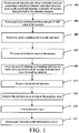
- FIG. 1 is a schematic flowchart of a manufacturing method of a semiconductor device.
- FIG. 2 to FIG. 11 illustrate schematically cross-sectional views of several phases of a manufacturing process of a semiconductor device.
- FIG. 12 illustrates schematically a perspective view of a semiconductor device.
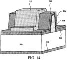
- FIG. 13 and FIG. 14 illustrate schematically a cross-sectional view and a perspective view of a semiconductor device according to another form of the present invention. The following describes the forms of the present invention with reference to FIG. 1 to FIG. 14 .
- step 101 a substrate structure is formed.
- the substrate may include a sacrificial substrate 200 and a first dielectric layer 202 on the sacrificial substrate 200.
- a plurality of recesses 203 are formed in the substrate to provide the substrate structure 201.
- the recesses 203 may be formed in the first dielectric layer 202 and bottom portions and part of side walls of the recesses 203 may be located in the sacrificial substrate 200.
- the recesses 203 may be formed through the first dielectric layer 202 and into the sacrificial substrate 200.
- a material of the sacrificial substrate 200 may include a semiconductor material such as silicon.
- a material of the first dielectric layer 202 comprises a dielectric material on which graphene cannot be selectively grown (see FIG. 5 for how to avoid growing graphene on the first dielectric layer in subsequent steps of selectively growing a graphene layer).
- a material for the first dielectric layer 202 may comprise an oxide of silicon.
- the substrate structure 201 of the present invention may be formed by using methods, process steps, and materials known in this field. Therefore, details of a process of forming the substrate structure 201 are not described herein in detail.
- each of the recesses 203 of the substrate structure 201 may comprise an elongated groove.
- step 103 a buffer layer at bottom portions and part of side walls of the recesses is formed.
- a buffer layer 204 may be formed at bottom portions and part of the side walls of the recesses 203 by using, e.g., an epitaxial growth process.
- the buffer layer may be alternatively referred to as a pad layer.
- the buffer layer will be used to facilitate a growth of graphene.
- a material of the buffer layer 204 may include silicon germanium, or another material known by a person of ordinary skill in the art and on which graphene can be selectively grown.
- step 105 a graphene layer is selectively grown on the buffer layer.
- a graphene layer 206 may be selectively grown on the buffer layer 204 as shown in FIG. 4 , using, for example, methane and hydrogen.
- the graphene layer 206 may also be selectively grown on the buffer layer 204 using another process for selective growth of graphene that is known by a person of ordinary skill in the art.
- a material of the first dielectric layer 202 may comprise a dielectric material on which graphene cannot be selectively grown. Therefore, no graphene layer may be grown on top portions and side walls of the first dielectric layer 202, as shown in FIG. 4 .
- step 107 the recesses is filled with a second dielectric layer.
- a second dielectric layer 207 is used to fill the recesses 203 by using, for example, an atomic layer deposition (ALD) process or a physical vapor deposition (PVD) process.
- a preferable process for depositing the second dielectric layer may be chosen so as to avoid introducing oxygen into the graphene layer 206. Introduction of oxygen into the graphene layer may adversely affect the performance of a resulting device.
- processes such as a chemical vapor deposition (CVD) process may introduce oxygen into the graphene layer and may not be a preferable process for depositing the second dielectric layer 207.
- a material of the second dielectric layer 207 may include: a nonconductive nitride of boron or an oxide of silicon.
- the second dielectric layer 207 may be preferably deposited using the PVD process.
- a planarization process may be performed after step 107, so that a top portion of the second dielectric layer 207 in the recesses approximately flushes top portions of the first dielectric layer 202 between the recesses, as shown in FIG. 6 .
- each of the recesses 203 may comprise an elongated groove, so that the second dielectric layer 207 filled in the recesses 203 forms a fin 208, as shown in FIG. 6 .
- the buffer layer 204 may be formed to cover top portions and side walls of the first dielectric layer 202.
- the graphene layer 206 is selectively grown on the buffer layer 204.
- the second dielectric layer 207 is deposited to cover the graphene layer 206, where the second dielectric layer 207 further fills the recesses 203.
- a planarization process is performed, so that top portions of the second dielectric layer 207 in the recess approximately flushes with the top portion of the first dielectric layer 202 between the recesses.
- a buffer layer 204 and a graphene layer 206 are also grown on side walls of the first dielectric layer 202 (not shown in FIG. 6 ).
- the buffer layer 204 may be formed to cover top portions of the first dielectric layer 202.
- an alumina layer may be formed on the structure shown in FIG. 2 through deposition (for example, atomic layer deposition (ALD)); and then a part of the alumina layer at a top portion may be removed by using a patterned mask, so as to form a structure shown in FIG. 3 .
- the graphene layer 206 is selectively grown on the buffer layer 204. Afterwards, process steps similar to those described above may be performed.
- step 109 the growth substrate is further attached to a bonding substrate.
- the growth substrate is attached to a bonding substrate 300 in a manner that top portion of the second dielectric layer 207 (i.e., the base portion of the fin 208 or the side of the growth substrate facing away from the sacrificial substrate layer 200) faces the bonding substrate 300.
- the growth substrate may be attached to the bonding substrate 300 by means of solid solution, interference fit, or bonding (e.g., through hydrogen bonding at a surface).
- a material of the bonding substrate 300 may include a semiconductor material such as silicon.
- a dielectric layer 302 may also be formed on a surface of the bonding substrate 300 that is opposite to a bonding surface at which the bonding substrate 300 is attached to the growth substrate, as shown in FIG. 7 .
- step 111 the sacrificial substrate is removed.
- the sacrificial substrate 200 is removed, as shown in FIG. 8 , by using an etching agent according to a wet etching process.
- the etching agent may include, for example, tetramethylammonium hydroxide (TMAH), or a mixed solution of ammonium hydroxide and hydrochloric acid.
- step 113 the buffer layer is removed so as to expose the graphene layer, as shown in FIG. 9 .
- the buffer layer 204 may comprise silicon germanium (SiGe) and may be removed by using a mixed solution of ammonium hydroxide and hydrochloric acid, so as to expose the graphene layer 206, as shown in FIG. 9 .
- the buffer layer 204 may also be removed, under a condition that the graphene layer 206 is not damaged, by using another method known by a person of ordinary skill in the art.
- a third dielectric layer 210 may be further formed in step 115.
- the third dielectric layer 210 at least covers part of the exposed graphene layer 206.
- a material of the third dielectric layer 210 may include a nonconductive nitride of boron or an oxide of silicon.
- the third dielectric layer 210 may be formed using a PVD process.
- the third dielectric layer 210 may also be formed using another method known by a person of ordinary skill in the art.
- a gate electrode on the third dielectric layer may be further formed in step 117.
- a gate electrode 212 is formed on the third dielectric layer 210. It should be understood that the gate electrode of the present invention may be formed by using methods, process steps, and materials known in this field. Therefore, details of a process of forming the gate electrode are not described herein.
- a perspective view of an semiconductor device obtained from the process above and comprising one fin 208 is shown in FIG. 12 .
- FIG. 13 A cross-sectional diagram of a semiconductor device obtained according to another implementation of a manufacturing method of the foregoing semiconductor device is shown in FIG. 13 , where a graphene layer 206 is also grown on a side wall of the first dielectric layer 202.
- FIG. 14 A perspective view of the semiconductor device obtained by using this method is shown in FIG. 14 .
- the manufacturing methods of the semiconductor device in the forms above may reduce complexity of patterning the graphene layer by selectively growing a graphene layer on a patterned buffer layer, thereby avoiding adverse effects from patterning graphene using etching processes such as direct laser raster writing or photoetching.
- this disclosure further teaches a semiconductor device, including: a substrate, a fin structure on the substrate, and a graphene layer covering a top portion and at least an upper portion of a side wall of each fin of the fin structure.
- a first dielectric layer on the substrate and between the fin structures is further included.
- the graphene layer is above the first dielectric layer.
- the fin structure comprises a second dielectric material.
- the fin structure comprises a surface layer formed by an insulating material.
- the second dielectric material comprises an oxide of silicon.
- the first dielectric layer comprises a dielectric material on which graphene cannot be selectively grown.
- the second dielectric layer comprises a nonconductive nitride of boron or an oxide of silicon.
- the substrate layer comprises silicon
- a third dielectric layer covering the graphene layer is further included.
- the third dielectric layer comprises a nonconductive nitride of boron or an oxide of silicon.
- a gate electrode covering a part of a top portion and a part of a side wall of each fin of the fin structure is further included.
Landscapes
- Thin Film Transistor (AREA)
- Insulated Gate Type Field-Effect Transistor (AREA)
- Carbon And Carbon Compounds (AREA)
Abstract
Description
- This application is based on and claims priority to Chinese Patent Application
CN201610871131.6, filed September 30, 2016 - The present invention relates to the technical field of semiconductor technologies, particularly to a semiconductor device and a manufacturing method thereof, and more specifically to a graphene semiconductor device and a manufacturing method thereof.
- Graphene is a two-dimensional crystalline material of carbon atoms, and possess special features such as a forbidden electronic band gap with zero width and high carrier mobility. Since its discovery in 2004, graphene is expected to be used to develop a new generation of electric elements such as transistors that are thinner and of high electric conduction speed.
- Existing methods for patterning graphene mainly include a method of photolithography and a method of direct laser raster writing. Although the method of direct laser raster writing introduces no other chemical reagents during a process of patterning the graphene, a patterned feature in the graphene layer obtained using this method may not be fine enough (i.e., may be of insufficient resolution) and a long production cycle. Moreover, the method of photolithography introduces other chemical reagents during etching, and a developing solution and a stripping solution used thereby for, e.g., photoresists, may be problematic. For example, photolithography of graphene may lead to increase in sheet resistance of the obtained patterned graphene.
- Therefore, development of technologies related to manufacturing a high-quality semiconductor device having a patterned graphene layer represents one of the major current challenges in semi-conductor technologies.
- It is an object of the present invention to provide a method of for manufacturing a semiconductor device and a semiconductor device which address at least one of the foregoing problems., in particular in connection with high-quality semiconductor devices having a patterned graphene layer.
- The object is achieved by the features of the respective independent claims. Further embodiments are defined in the respective dependent claims.
- A first aspect of the present invention provides a method for manufacturing a semiconductor device. The method includes: providing a growth substrate, wherein the growth substrate contains a sacrificial substrate and a first dielectric layer on the sacrificial substrate, a plurality of recesses formed through the first dielectric layer and into the sacrificial substrate, a buffer layer covering surfaces of the plurality of recess, a selectively grown graphene layer on the buffer layer, and a second dielectric layer filling the plurality of recesses. The method further includes attaching the growth substrate to a bonding substrate such that the second dielectric layer attaches to the bonding substrate; removing the sacrificial substrate; and removing the buffer layer so as to expose the graphene layer.
- Preferably, providing the growth substrate comprises forming a growth substrate, where the forming a growth substrate includes: forming a growth substrate by providing a substrate structure containing a sacrificial substrate, a first dielectric layer on the sacrificial substrate, and a plurality of recesses formed through the first dielectric layer and into the sacrificial substrate, by forming a buffer layer covering exposes surfaces of the plurality of recesses, by selectively growing a graphene layer on the buffer layer, and by filling the plurality of recesses with a second dielectric layer.
- The method of present invention avoids adverse effects from patterning graphene by using selective growth of graphene on a patterned buffer layer.
- Preferably, forming (or providing) the growth substrate further includes: performing planarization after filling the plurality of recesses with the second dielectric layer so that the second dielectric layer in the plurality of recesses approximately flushes with the first dielectric layer between the plurality of recesses.
- Preferably, forming the buffer layer covering the exposed surfaces of the plurality of recesses above includes forming, by using an epitaxial growth process, the buffer layer covering the exposed surfaces of the plurality of recesses.
- Preferably, filling the plurality of recesses with the second dielectric layer includes: filling the plurality of recesses with the second dielectric layer using an atomic layer deposition process or a physical vapor deposition process.
- Preferably, the second dielectric layer above includes a nonconductive nitride of boron, or an oxide of silicon.
- Preferably, selectively growing the graphene layer includes selectively growing the graphene layer on the buffer layer using methane and hydrogen.
- Preferably, the sacrificial substrate above includes silicon.
- Preferably, removing the sacrificial substrate includes using an etching agent to remove the sacrificial substrate in a wet etching process.
- Preferably, the etching agent above includes tetramethylammonium hydroxide.
- Preferably, the buffer layer above includes silicon germanium.
- Preferably, removing the buffer layer includes removing the buffer layer using a mixed solution of ammonium hydroxide and hydrochloric acid.
- Preferably, the foregoing methods further include forming a third dielectric layer to cover at least part of the exposed graphene layer.
- Preferably, the third dielectric layer above includes a nonconductive nitride of boron, or an oxide of silicon.
- Preferably, forming the gate electrode on the third dielectric layer above is further included.
- Preferably, the plurality of recesses above each comprises an elongated groove; the second dielectric layer filling the plurality of recesses forms a plurality of fins; the exposed graphene layer covers at least part of the plurality of fins; and the graphene layer and the second dielectric layer form a fin structure.
- Preferably, the methods above further include: forming a third dielectric layer to cover at least part of the exposed graphene layer; and forming a gate electrode on the third dielectric layer.
- Preferably, the first dielectric layer includes a dielectric material on which graphene cannot be selectively grown.
- A second aspect of the present invention provides a first alternative of a semiconductor device. The semiconductor device includes: a substrate; a fin structure on the substrate; and a graphene layer covering at least a portion of the fin structure.
- Preferably, the fin structure in the semiconductor device above includes a plurality of fins and the semiconductor device above further includes a first dielectric layer on the substrate and between the fin structures.
- Preferably, the graphene layer is provided above the first dielectric layer in the semiconductor device above.
- Preferably, the find of the fin structure in the semiconductor device above is comprises a second dielectric material.
- Preferably, the fin structure of the semiconductor device above includes a surface layer of an insulating material.
- Preferably, the second dielectric material for the semiconductor device above includes an oxide of silicon.
- Preferably, the first dielectric layer for the semiconductor device above comprises a dielectric material on which graphene cannot be selectively grown.
- Preferably, second dielectric layer for the semiconductor device above comprises a nonconductive nitride of boron, or an oxide of silicon.
- Preferably, the substrate layer above includes silicon.
- Preferably, a third dielectric layer covering the graphene layer is further included in the semiconductor device above.
- Preferably, the third dielectric layer above includes a nonconductive nitride of boron, or an oxide of silicon.
- Preferably, a gate electrode covering part of the third dielectric layer is further included in the semiconductor device above.
- A semiconductor device according to the second aspect of the present invention may be obtained by a method according to the first aspect of the present invention.
- According to the following detailed descriptions of the exemplary forms of the present invention with reference to the accompanying drawings, other characters and advantages of the present invention will become clear.
- The accompanying drawings that form a part of the specification describe forms of the present invention, and are used to explain the principles of the present invention together with the specification.
- With reference to the accompanying drawings, the present invention can be understood more clearly according to the following detailed description, where:
-
FIG. 1 is a schematic flowchart of a manufacturing method of a semiconductor device; -
FIG. 2 to FIG. 11 illustrate schematically cross-sectional views of several phases of a manufacturing process of a semiconductor device; -
FIG. 12 illustrates schematically a perspective view of a semiconductor device; -
FIG. 13 illustrates schematically a cross-sectional view of a semiconductor device; and -
FIG. 14 illustrates schematically a perspective view of another semiconductor device. - Exemplary forms of the present invention are described in detail with reference to the accompanying drawings. It should be noted that unless being described in detail, relative layouts, mathematical expressions, and numeric values of components and steps described in these forms do not limit the present invention.
- In addition, it should be noted that for ease of description, sizes of the parts shown in the accompanying drawings are not drawn according to any actual proportional relationship.
- The following description about at least one exemplary form actually is illustrative only, and would not be used as any limitation on the present invention and applications or uses of the present invention.
- Technologies, methods, and devices that are known by a person of ordinary skill in the related fields may not be discussed in detail. However, if appropriate, these technologies, methods, and devices should be considered as a part of the description.
- In all examples shown and discussed herein, any specific value should be interpreted to be illustrative only rather than a limitation. Therefore, other examples of the exemplary forms may have different values.
- It should be noted that similar reference numerals, labels, and letters represent similar items in the following accompanying drawings. Therefore, once an item is defined in a figure, the item may be but needs not to be further discussed in subsequent figures.
-
FIG. 1 is a schematic flowchart of a manufacturing method of a semiconductor device.FIG. 2 to FIG. 11 illustrate schematically cross-sectional views of several phases of a manufacturing process of a semiconductor device.FIG. 12 illustrates schematically a perspective view of a semiconductor device.FIG. 13 andFIG. 14 illustrate schematically a cross-sectional view and a perspective view of a semiconductor device according to another form of the present invention. The following describes the forms of the present invention with reference toFIG. 1 to FIG. 14 . - As shown in
FIG. 1 , instep 101, a substrate structure is formed. - First, a substrate is provided. As shown in
FIG. 2 , the substrate may include asacrificial substrate 200 and a firstdielectric layer 202 on thesacrificial substrate 200. A plurality ofrecesses 203 are formed in the substrate to provide thesubstrate structure 201. Specifically, therecesses 203 may be formed in thefirst dielectric layer 202 and bottom portions and part of side walls of therecesses 203 may be located in thesacrificial substrate 200. In other words, therecesses 203 may be formed through thefirst dielectric layer 202 and into thesacrificial substrate 200. A material of thesacrificial substrate 200 may include a semiconductor material such as silicon. - In an implementation, a material of the
first dielectric layer 202 comprises a dielectric material on which graphene cannot be selectively grown (seeFIG. 5 for how to avoid growing graphene on the first dielectric layer in subsequent steps of selectively growing a graphene layer). For example, a material for thefirst dielectric layer 202 may comprise an oxide of silicon. - It should be understood that the
substrate structure 201 of the present invention may be formed by using methods, process steps, and materials known in this field. Therefore, details of a process of forming thesubstrate structure 201 are not described herein in detail. - In an implementation, each of the
recesses 203 of thesubstrate structure 201 may comprise an elongated groove. - Back to
FIG. 1 , instep 103, a buffer layer at bottom portions and part of side walls of the recesses is formed. - In an implementation, as shown in
FIG. 3 , abuffer layer 204 may be formed at bottom portions and part of the side walls of therecesses 203 by using, e.g., an epitaxial growth process. The buffer layer may be alternatively referred to as a pad layer. The buffer layer will be used to facilitate a growth of graphene. A material of thebuffer layer 204 may include silicon germanium, or another material known by a person of ordinary skill in the art and on which graphene can be selectively grown. - Subsequently, as shown in
FIG. 1 , instep 105, a graphene layer is selectively grown on the buffer layer. - In an implementation, a
graphene layer 206 may be selectively grown on thebuffer layer 204 as shown inFIG. 4 , using, for example, methane and hydrogen. Thegraphene layer 206 may also be selectively grown on thebuffer layer 204 using another process for selective growth of graphene that is known by a person of ordinary skill in the art. - In an implementation, a material of the
first dielectric layer 202 may comprise a dielectric material on which graphene cannot be selectively grown. Therefore, no graphene layer may be grown on top portions and side walls of thefirst dielectric layer 202, as shown inFIG. 4 . - Subsequently, as shown in
FIG. 1 , instep 107, the recesses is filled with a second dielectric layer. - In an implementation, as shown in
FIG. 5 , asecond dielectric layer 207 is used to fill therecesses 203 by using, for example, an atomic layer deposition (ALD) process or a physical vapor deposition (PVD) process. A preferable process for depositing the second dielectric layer may be chosen so as to avoid introducing oxygen into thegraphene layer 206. Introduction of oxygen into the graphene layer may adversely affect the performance of a resulting device. For example, processes such as a chemical vapor deposition (CVD) process may introduce oxygen into the graphene layer and may not be a preferable process for depositing thesecond dielectric layer 207. A material of thesecond dielectric layer 207 may include: a nonconductive nitride of boron or an oxide of silicon. When the material of thesecond dielectric layer 207 is an oxide of silicon, thesecond dielectric layer 207 may be preferably deposited using the PVD process. - In an implementation, a planarization process may be performed after
step 107, so that a top portion of thesecond dielectric layer 207 in the recesses approximately flushes top portions of thefirst dielectric layer 202 between the recesses, as shown inFIG. 6 . In a specific implementation, each of therecesses 203 may comprise an elongated groove, so that thesecond dielectric layer 207 filled in therecesses 203 forms afin 208, as shown inFIG. 6 . - In another alternative implementation, in
step 103, thebuffer layer 204 may be formed to cover top portions and side walls of thefirst dielectric layer 202. Subsequently, instep 105, thegraphene layer 206 is selectively grown on thebuffer layer 204. Subsequently, instep 107, thesecond dielectric layer 207 is deposited to cover thegraphene layer 206, where thesecond dielectric layer 207 further fills therecesses 203. Afterwards, a planarization process is performed, so that top portions of thesecond dielectric layer 207 in the recess approximately flushes with the top portion of thefirst dielectric layer 202 between the recesses. In this implementation manner, abuffer layer 204 and agraphene layer 206 are also grown on side walls of the first dielectric layer 202 (not shown inFIG. 6 ). - In another implementation alternative to the implementations above, in
step 103, thebuffer layer 204 may be formed to cover top portions of thefirst dielectric layer 202. For example, an alumina layer may be formed on the structure shown inFIG. 2 through deposition (for example, atomic layer deposition (ALD)); and then a part of the alumina layer at a top portion may be removed by using a patterned mask, so as to form a structure shown inFIG. 3 . Subsequently, instep 105, thegraphene layer 206 is selectively grown on thebuffer layer 204. Afterwards, process steps similar to those described above may be performed. - The structure obtained above as shown in
FIG 6 may be referred to as a growth substrate. Returning toFIG. 1 , instep 109, the growth substrate is further attached to a bonding substrate. - In an implementation, as shown in
FIG. 7 , the growth substrate is attached to abonding substrate 300 in a manner that top portion of the second dielectric layer 207 (i.e., the base portion of thefin 208 or the side of the growth substrate facing away from the sacrificial substrate layer 200) faces thebonding substrate 300. For example, the growth substrate may be attached to thebonding substrate 300 by means of solid solution, interference fit, or bonding (e.g., through hydrogen bonding at a surface). A material of thebonding substrate 300 may include a semiconductor material such as silicon. Optionally, adielectric layer 302 may also be formed on a surface of thebonding substrate 300 that is opposite to a bonding surface at which thebonding substrate 300 is attached to the growth substrate, as shown inFIG. 7 . - Subsequently, in
step 111, the sacrificial substrate is removed. - In an implementation, the
sacrificial substrate 200 is removed, as shown inFIG. 8 , by using an etching agent according to a wet etching process. Depending on the material used for thesacrificial substrate 200, the etching agent may include, for example, tetramethylammonium hydroxide (TMAH), or a mixed solution of ammonium hydroxide and hydrochloric acid. - Subsequently, in
step 113, the buffer layer is removed so as to expose the graphene layer, as shown inFIG. 9 . - In an implementation, the
buffer layer 204 may comprise silicon germanium (SiGe) and may be removed by using a mixed solution of ammonium hydroxide and hydrochloric acid, so as to expose thegraphene layer 206, as shown inFIG. 9 . Thebuffer layer 204 may also be removed, under a condition that thegraphene layer 206 is not damaged, by using another method known by a person of ordinary skill in the art. - Optionally, as shown in
FIG. 1 , a thirddielectric layer 210 may be further formed instep 115. - As shown in
FIG. 10 , the thirddielectric layer 210 at least covers part of the exposedgraphene layer 206. A material of the thirddielectric layer 210 may include a nonconductive nitride of boron or an oxide of silicon. For example, the thirddielectric layer 210 may be formed using a PVD process. The thirddielectric layer 210 may also be formed using another method known by a person of ordinary skill in the art. - Optionally, as shown in
FIG. 1 , a gate electrode on the third dielectric layer may be further formed instep 117. - As shown in
FIG. 11 , agate electrode 212 is formed on the thirddielectric layer 210. It should be understood that the gate electrode of the present invention may be formed by using methods, process steps, and materials known in this field. Therefore, details of a process of forming the gate electrode are not described herein. A perspective view of an semiconductor device obtained from the process above and comprising onefin 208 is shown inFIG. 12 . - A cross-sectional diagram of a semiconductor device obtained according to another implementation of a manufacturing method of the foregoing semiconductor device is shown in
FIG. 13 , where agraphene layer 206 is also grown on a side wall of thefirst dielectric layer 202. A perspective view of the semiconductor device obtained by using this method is shown inFIG. 14 . - The manufacturing methods of the semiconductor device in the forms above may reduce complexity of patterning the graphene layer by selectively growing a graphene layer on a patterned buffer layer, thereby avoiding adverse effects from patterning graphene using etching processes such as direct laser raster writing or photoetching.
- It should be understood that when an element (such as a layer, an area, or a substrate) is called as being on another element, the element may be directly on the another element or there may also be an intermediate element. In addition, a relative term such as "below..." or "above..." may be used herein to describe a relationship of a layer or an area relative to another layer or area. It should also be understood that these terms are aimed at including different orientations of a device besides an orientation described in the accompanying drawings. As used herein, the term "and/or" includes any or all combinations of one or more of listed items that are associated with each other, and may also be abbreviated as "/".
- It should be understood that this disclosure further teaches a semiconductor device, including: a substrate, a fin structure on the substrate, and a graphene layer covering a top portion and at least an upper portion of a side wall of each fin of the fin structure.
- In an implementation, a first dielectric layer on the substrate and between the fin structures is further included.
- In an implementation, the graphene layer is above the first dielectric layer.
- In an implementation, the fin structure comprises a second dielectric material.
- In an implementation, the fin structure comprises a surface layer formed by an insulating material.
- In an implementation, the second dielectric material comprises an oxide of silicon.
- In an implementation, the first dielectric layer comprises a dielectric material on which graphene cannot be selectively grown.
- In an implementation, the second dielectric layer comprises a nonconductive nitride of boron or an oxide of silicon.
- In an implementation, the substrate layer comprises silicon.
- In an implementation, a third dielectric layer covering the graphene layer is further included.
- In an implementation, the third dielectric layer comprises a nonconductive nitride of boron or an oxide of silicon.
- In an implementation, a gate electrode covering a part of a top portion and a part of a side wall of each fin of the fin structure is further included.
- Heretofore, a semiconductor device and a manufacturing method thereof according to the forms of this disclosure are described in detail. To avoid obscuring the teaching of this disclosure, some details generally known in this field are not described.
Claims (15)
- A method for manufacturing a semiconductor device, comprising:providing a growth substrate, wherein the growth substrate comprises:a sacrificial substrate and a first dielectric layer on the sacrificial substrate;a plurality of recesses formed through the first dielectric layer and into the sacrificial substrate;a buffer layer covering surfaces of the plurality of recess;a selectively grown graphene layer on the buffer layer; anda second dielectric layer filling the plurality of recesses;attaching the growth substrate to a bonding substrate such that the second dielectric layer attaches to the bonding substrate;removing the sacrificial substrate; andremoving the buffer layer so as to expose the graphene layer.
- The method according to claim 1, wherein providing the growth substrate comprises:providing a substrate structure comprising the sacrificial substrate, the first dielectric layer on the sacrificial substrate, and the plurality of recesses formed through the first dielectric layer and into the sacrificial substrate;forming the buffer layer covering exposed surfaces of the plurality of recesses;selectively growing the graphene layer on the buffer layer; andfilling the plurality of recesses with the second dielectric layer.
- The method according to claim 2, wherein providing the growth substrate further comprises:performing planarization after filling the plurality of recesses with the second dielectric layer so that the second dielectric layer in the plurality of recesses approximately flushes with the first dielectric layer between the plurality of recesses.
- The method according to claim 2 or 3, wherein forming the buffer layer covering the exposed surfaces of the plurality of recesses comprises:forming, by using an epitaxial growth process, the buffer layer covering the exposed surfaces of the plurality of recesses.
- The method according to anyone of the claims 2-4, wherein filling of the plurality of recesses with the second dielectric layer comprises:filling the plurality of recesses with the second dielectric layer using an atomic layer deposition process or a physical vapor deposition process.
- The method according to anyone of the claims 2-5, wherein selectively growing the graphene layer comprises:selectively growing the graphene layer on the buffer layer using methane and hydrogen.
- The method according to anyone of the claims 1-6, wherein removing the sacrificial substrate comprises using an etching agent to remove the sacrificial substrate in a wet etching process.
- The method according to anyone of the claim 1, further comprising:forming a third dielectric layer to cover at least part of the exposed graphene layer; andpreferably, forming a gate electrode on the third dielectric layer.
- The method according to anyone of the claim 1-8, wherein:the plurality of recesses each comprises an elongated groove;the second dielectric layer filling the plurality of recesses forms a plurality of fins;the exposed graphene layer covers at least part of the plurality of fins; andthe graphene layer and the second dielectric layer form a fin structure; andwherein the method preferably further comprises: forming a third dielectric layer to cover at least part of the exposed graphene layer; and forming a gate electrode on the third dielectric layer.
- The method according to anyone of the claims 1-9, wherein the first dielectric layer comprises a dielectric material on which graphene cannot be grown.
- A semiconductor device, comprising:a substrate;a fin structure on the substrate; anda graphene layer covering at least a portion of the fin structure.
- The semiconductor device according to claim 11, wherein the fin structure comprises a plurality of fins, and wherein the semiconductor device further comprises:a first dielectric layer on the substrate and between the plurality of fins.
- The semiconductor device according to claim 12, wherein
the graphene layer is above the first dielectric layer; and/or
the first dielectric layer comprises a dielectric material on which graphene cannot be grown. - The semiconductor device according to anyone of the claims 11-13, wherein:fins of the fin structure comprises a second dielectric material; and/orthe fin structure comprises a surface layer of an insulating material.
- The semiconductor device according to anyone of the claims 11-13, further comprising
a third dielectric layer covering the graphene layer; and
preferably, a gate electrode covering part of the third dielectric layer.
Applications Claiming Priority (1)
| Application Number | Priority Date | Filing Date | Title |
|---|---|---|---|
| CN201610871131.6A CN107887261B (en) | 2016-09-30 | 2016-09-30 | Semiconductor device and method of manufacturing the same |
Publications (1)
| Publication Number | Publication Date |
|---|---|
| EP3301703A1 true EP3301703A1 (en) | 2018-04-04 |
Family
ID=59799232
Family Applications (1)
| Application Number | Title | Priority Date | Filing Date |
|---|---|---|---|
| EP17188984.3A Withdrawn EP3301703A1 (en) | 2016-09-30 | 2017-09-01 | Semiconductor device and manufacturing method thereof |
Country Status (3)
| Country | Link |
|---|---|
| US (1) | US10134849B2 (en) |
| EP (1) | EP3301703A1 (en) |
| CN (1) | CN107887261B (en) |
Families Citing this family (2)
| Publication number | Priority date | Publication date | Assignee | Title |
|---|---|---|---|---|
| US11271094B2 (en) | 2018-11-29 | 2022-03-08 | Taiwan Semiconductor Manufacturing Company Ltd. | Semiconductor structure and method of manufacturing the same |
| CN118899316A (en) * | 2023-05-04 | 2024-11-05 | 无锡晶湛半导体有限公司 | A composite substrate and a method for manufacturing the same, and a semiconductor structure |
Citations (4)
| Publication number | Priority date | Publication date | Assignee | Title |
|---|---|---|---|---|
| US20130146846A1 (en) * | 2011-12-13 | 2013-06-13 | International Business Machines Corporation | Graphene field effect transistor |
| US20140015015A1 (en) * | 2012-07-10 | 2014-01-16 | Globalfoundries Inc. | Finfet device with a graphene gate electrode and methods of forming same |
| US20150364592A1 (en) * | 2014-06-13 | 2015-12-17 | Taiwan Semiconductor Manufacturing Company, Ltd. | Thin-Sheet FinFET Device |
| US20160013184A1 (en) * | 2014-07-08 | 2016-01-14 | International Business Machines Corporation | Method and structure to suppress finfet heating |
Family Cites Families (2)
| Publication number | Priority date | Publication date | Assignee | Title |
|---|---|---|---|---|
| CN105575814B (en) * | 2014-10-17 | 2019-01-22 | 中芯国际集成电路制造(上海)有限公司 | Fin formula field effect transistor and forming method thereof |
| US9972537B2 (en) * | 2016-02-24 | 2018-05-15 | Globalfoundries Inc. | Methods of forming graphene contacts on source/drain regions of FinFET devices |
-
2016
- 2016-09-30 CN CN201610871131.6A patent/CN107887261B/en active Active
-
2017
- 2017-08-22 US US15/683,237 patent/US10134849B2/en active Active
- 2017-09-01 EP EP17188984.3A patent/EP3301703A1/en not_active Withdrawn
Patent Citations (4)
| Publication number | Priority date | Publication date | Assignee | Title |
|---|---|---|---|---|
| US20130146846A1 (en) * | 2011-12-13 | 2013-06-13 | International Business Machines Corporation | Graphene field effect transistor |
| US20140015015A1 (en) * | 2012-07-10 | 2014-01-16 | Globalfoundries Inc. | Finfet device with a graphene gate electrode and methods of forming same |
| US20150364592A1 (en) * | 2014-06-13 | 2015-12-17 | Taiwan Semiconductor Manufacturing Company, Ltd. | Thin-Sheet FinFET Device |
| US20160013184A1 (en) * | 2014-07-08 | 2016-01-14 | International Business Machines Corporation | Method and structure to suppress finfet heating |
Also Published As
| Publication number | Publication date |
|---|---|
| US20180097068A1 (en) | 2018-04-05 |
| CN107887261B (en) | 2020-11-06 |
| US10134849B2 (en) | 2018-11-20 |
| CN107887261A (en) | 2018-04-06 |
Similar Documents
| Publication | Publication Date | Title |
|---|---|---|
| US9461149B2 (en) | Nanowire structure with selected stack removed for reduced gate resistance and method of fabricating same | |
| JP5095812B2 (en) | Core-shell-shell nanowire transistor and manufacturing method thereof | |
| US11929286B2 (en) | Two dimension material fin sidewall | |
| CN105633167B (en) | Semiconductor device having high quality epitaxial layer and method of manufacturing the same | |
| CN105633166A (en) | Nanowire semiconductor device with high-quality epitaxial layer and its manufacturing method | |
| US9716045B2 (en) | Directly forming SiGe fins on oxide | |
| US10002876B2 (en) | FinFET vertical flash memory | |
| CN108735604A (en) | The forming method of transistor | |
| US9954106B2 (en) | III-V fin on insulator | |
| US10134849B2 (en) | Semiconductor device and manufacturing method thereof | |
| US20180061942A1 (en) | Structure and process to tuck fin tips self-aligned to gates | |
| US20230012216A1 (en) | Gate all around transistor with dual inner spacers | |
| CN109037214A (en) | A kind of semiconductor devices and preparation method thereof and electronic device | |
| WO2017096780A1 (en) | Semiconductor device having high-quality epitaxial layer and method for manufacturing same | |
| US10157751B1 (en) | Method for manufacturing semiconductor device | |
| CN106098776A (en) | Nanowire semiconductor device with high-quality epitaxial layer and its manufacturing method | |
| CN107564818A (en) | Semiconductor device and its manufacture method | |
| CN107665824A (en) | A kind of FinFET and preparation method, electronic installation | |
| US10121872B2 (en) | Method for forming a semiconductor device comprising a selectively grown graphene layer | |
| CN107706113A (en) | A kind of FinFET and preparation method, electronic installation | |
| CN106098623B (en) | Semiconductor device having high quality epitaxial layer and method of manufacturing the same | |
| CN107785272A (en) | A kind of SQW FinFET and preparation method thereof, electronic installation | |
| CN108630547A (en) | FINFET device and preparation method thereof |
Legal Events
| Date | Code | Title | Description |
|---|---|---|---|
| PUAI | Public reference made under article 153(3) epc to a published international application that has entered the european phase |
Free format text: ORIGINAL CODE: 0009012 |
|
| STAA | Information on the status of an ep patent application or granted ep patent |
Free format text: STATUS: THE APPLICATION HAS BEEN PUBLISHED |
|
| AK | Designated contracting states |
Kind code of ref document: A1 Designated state(s): AL AT BE BG CH CY CZ DE DK EE ES FI FR GB GR HR HU IE IS IT LI LT LU LV MC MK MT NL NO PL PT RO RS SE SI SK SM TR |
|
| AX | Request for extension of the european patent |
Extension state: BA ME |
|
| STAA | Information on the status of an ep patent application or granted ep patent |
Free format text: STATUS: REQUEST FOR EXAMINATION WAS MADE |
|
| 17P | Request for examination filed |
Effective date: 20180515 |
|
| RBV | Designated contracting states (corrected) |
Designated state(s): AL AT BE BG CH CY CZ DE DK EE ES FI FR GB GR HR HU IE IS IT LI LT LU LV MC MK MT NL NO PL PT RO RS SE SI SK SM TR |
|
| RAP1 | Party data changed (applicant data changed or rights of an application transferred) |
Owner name: SEMICONDUCTOR MANUFACTURING INTERNATIONAL (SHANGHA Owner name: SEMICONDUCTOR MANUFACTURING INTERNATIONAL (BEIJING |
|
| STAA | Information on the status of an ep patent application or granted ep patent |
Free format text: STATUS: EXAMINATION IS IN PROGRESS |
|
| 17Q | First examination report despatched |
Effective date: 20191025 |
|
| STAA | Information on the status of an ep patent application or granted ep patent |
Free format text: STATUS: THE APPLICATION IS DEEMED TO BE WITHDRAWN |
|
| 18D | Application deemed to be withdrawn |
Effective date: 20200305 |