EP3300119A1 - Solid-source diffused junction for fin-based electronics - Google Patents
Solid-source diffused junction for fin-based electronics Download PDFInfo
- Publication number
- EP3300119A1 EP3300119A1 EP17196788.8A EP17196788A EP3300119A1 EP 3300119 A1 EP3300119 A1 EP 3300119A1 EP 17196788 A EP17196788 A EP 17196788A EP 3300119 A1 EP3300119 A1 EP 3300119A1
- Authority
- EP
- European Patent Office
- Prior art keywords
- fin
- end portion
- channel
- gate
- layer
- Prior art date
- Legal status (The legal status is an assumption and is not a legal conclusion. Google has not performed a legal analysis and makes no representation as to the accuracy of the status listed.)
- Ceased
Links
- 239000002019 doping agent Substances 0.000 claims abstract description 57
- 238000002955 isolation Methods 0.000 claims description 49
- 239000000463 material Substances 0.000 claims description 43
- 229910052710 silicon Inorganic materials 0.000 claims description 14
- 239000010703 silicon Substances 0.000 claims description 14
- 239000005360 phosphosilicate glass Substances 0.000 claims 18
- 239000005388 borosilicate glass Substances 0.000 claims 4
- QVGXLLKOCUKJST-UHFFFAOYSA-N atomic oxygen Chemical compound [O] QVGXLLKOCUKJST-UHFFFAOYSA-N 0.000 claims 2
- 229910052760 oxygen Inorganic materials 0.000 claims 2
- 239000001301 oxygen Substances 0.000 claims 2
- BHEPBYXIRTUNPN-UHFFFAOYSA-N hydridophosphorus(.) (triplet) Chemical group [PH] BHEPBYXIRTUNPN-UHFFFAOYSA-N 0.000 claims 1
- 239000011521 glass Substances 0.000 abstract description 78
- 239000000758 substrate Substances 0.000 abstract description 66
- 239000007787 solid Substances 0.000 abstract description 10
- 238000000034 method Methods 0.000 description 38
- 108091006146 Channels Proteins 0.000 description 37
- 229910021420 polycrystalline silicon Inorganic materials 0.000 description 26
- 229920005591 polysilicon Polymers 0.000 description 26
- 238000000151 deposition Methods 0.000 description 22
- 238000010586 diagram Methods 0.000 description 22
- 229910052751 metal Inorganic materials 0.000 description 15
- 239000002184 metal Substances 0.000 description 15
- 238000004891 communication Methods 0.000 description 13
- XUIMIQQOPSSXEZ-UHFFFAOYSA-N Silicon Chemical compound [Si] XUIMIQQOPSSXEZ-UHFFFAOYSA-N 0.000 description 12
- 239000010410 layer Substances 0.000 description 12
- 238000004519 manufacturing process Methods 0.000 description 12
- 125000006850 spacer group Chemical group 0.000 description 12
- 230000000903 blocking effect Effects 0.000 description 10
- 238000000059 patterning Methods 0.000 description 9
- 239000011800 void material Substances 0.000 description 9
- 238000000137 annealing Methods 0.000 description 7
- 238000009792 diffusion process Methods 0.000 description 7
- 238000005516 engineering process Methods 0.000 description 7
- 230000005669 field effect Effects 0.000 description 7
- 108010075750 P-Type Calcium Channels Proteins 0.000 description 5
- VYPSYNLAJGMNEJ-UHFFFAOYSA-N Silicium dioxide Chemical compound O=[Si]=O VYPSYNLAJGMNEJ-UHFFFAOYSA-N 0.000 description 4
- OKTJSMMVPCPJKN-UHFFFAOYSA-N Carbon Chemical compound [C] OKTJSMMVPCPJKN-UHFFFAOYSA-N 0.000 description 3
- 230000004888 barrier function Effects 0.000 description 3
- 229910052799 carbon Inorganic materials 0.000 description 3
- 239000004020 conductor Substances 0.000 description 3
- 230000008021 deposition Effects 0.000 description 3
- 238000009825 accumulation Methods 0.000 description 2
- 230000003190 augmentative effect Effects 0.000 description 2
- 230000015572 biosynthetic process Effects 0.000 description 2
- 238000005229 chemical vapour deposition Methods 0.000 description 2
- 229910044991 metal oxide Inorganic materials 0.000 description 2
- 150000004706 metal oxides Chemical class 0.000 description 2
- 238000012545 processing Methods 0.000 description 2
- 239000004065 semiconductor Substances 0.000 description 2
- 239000000377 silicon dioxide Substances 0.000 description 2
- 235000012239 silicon dioxide Nutrition 0.000 description 2
- 108090000699 N-Type Calcium Channels Proteins 0.000 description 1
- 102000004129 N-Type Calcium Channels Human genes 0.000 description 1
- ATJFFYVFTNAWJD-UHFFFAOYSA-N Tin Chemical compound [Sn] ATJFFYVFTNAWJD-UHFFFAOYSA-N 0.000 description 1
- 235000013405 beer Nutrition 0.000 description 1
- 239000000969 carrier Substances 0.000 description 1
- 230000001276 controlling effect Effects 0.000 description 1
- 238000007796 conventional method Methods 0.000 description 1
- 230000003247 decreasing effect Effects 0.000 description 1
- 230000001419 dependent effect Effects 0.000 description 1
- 238000005137 deposition process Methods 0.000 description 1
- 238000013461 design Methods 0.000 description 1
- 230000000694 effects Effects 0.000 description 1
- 230000005670 electromagnetic radiation Effects 0.000 description 1
- 238000005530 etching Methods 0.000 description 1
- -1 fin Substances 0.000 description 1
- 238000002513 implantation Methods 0.000 description 1
- 239000011229 interlayer Substances 0.000 description 1
- 230000007774 longterm Effects 0.000 description 1
- 230000001105 regulatory effect Effects 0.000 description 1
- 239000002210 silicon-based material Substances 0.000 description 1
- 238000003860 storage Methods 0.000 description 1
- 238000012546 transfer Methods 0.000 description 1
- WFKWXMTUELFFGS-UHFFFAOYSA-N tungsten Chemical compound [W] WFKWXMTUELFFGS-UHFFFAOYSA-N 0.000 description 1
- 229910052721 tungsten Inorganic materials 0.000 description 1
- 239000010937 tungsten Substances 0.000 description 1
Images


Classifications
-
- H—ELECTRICITY
- H01—ELECTRIC ELEMENTS
- H01L—SEMICONDUCTOR DEVICES NOT COVERED BY CLASS H10
- H01L29/00—Semiconductor devices adapted for rectifying, amplifying, oscillating or switching, or capacitors or resistors with at least one potential-jump barrier or surface barrier, e.g. PN junction depletion layer or carrier concentration layer; Details of semiconductor bodies or of electrodes thereof ; Multistep manufacturing processes therefor
- H01L29/02—Semiconductor bodies ; Multistep manufacturing processes therefor
- H01L29/06—Semiconductor bodies ; Multistep manufacturing processes therefor characterised by their shape; characterised by the shapes, relative sizes, or dispositions of the semiconductor regions ; characterised by the concentration or distribution of impurities within semiconductor regions
- H01L29/0603—Semiconductor bodies ; Multistep manufacturing processes therefor characterised by their shape; characterised by the shapes, relative sizes, or dispositions of the semiconductor regions ; characterised by the concentration or distribution of impurities within semiconductor regions characterised by particular constructional design considerations, e.g. for preventing surface leakage, for controlling electric field concentration or for internal isolations regions
- H01L29/0642—Isolation within the component, i.e. internal isolation
- H01L29/0649—Dielectric regions, e.g. SiO2 regions, air gaps
-
- H—ELECTRICITY
- H01—ELECTRIC ELEMENTS
- H01L—SEMICONDUCTOR DEVICES NOT COVERED BY CLASS H10
- H01L29/00—Semiconductor devices adapted for rectifying, amplifying, oscillating or switching, or capacitors or resistors with at least one potential-jump barrier or surface barrier, e.g. PN junction depletion layer or carrier concentration layer; Details of semiconductor bodies or of electrodes thereof ; Multistep manufacturing processes therefor
- H01L29/66—Types of semiconductor device ; Multistep manufacturing processes therefor
- H01L29/66007—Multistep manufacturing processes
- H01L29/66075—Multistep manufacturing processes of devices having semiconductor bodies comprising group 14 or group 13/15 materials
- H01L29/66227—Multistep manufacturing processes of devices having semiconductor bodies comprising group 14 or group 13/15 materials the devices being controllable only by the electric current supplied or the electric potential applied, to an electrode which does not carry the current to be rectified, amplified or switched, e.g. three-terminal devices
- H01L29/66409—Unipolar field-effect transistors
- H01L29/66893—Unipolar field-effect transistors with a PN junction gate, i.e. JFET
- H01L29/66901—Unipolar field-effect transistors with a PN junction gate, i.e. JFET with a PN homojunction gate
-
- H—ELECTRICITY
- H01—ELECTRIC ELEMENTS
- H01L—SEMICONDUCTOR DEVICES NOT COVERED BY CLASS H10
- H01L27/00—Devices consisting of a plurality of semiconductor or other solid-state components formed in or on a common substrate
- H01L27/02—Devices consisting of a plurality of semiconductor or other solid-state components formed in or on a common substrate including semiconductor components specially adapted for rectifying, oscillating, amplifying or switching and having at least one potential-jump barrier or surface barrier; including integrated passive circuit elements with at least one potential-jump barrier or surface barrier
- H01L27/04—Devices consisting of a plurality of semiconductor or other solid-state components formed in or on a common substrate including semiconductor components specially adapted for rectifying, oscillating, amplifying or switching and having at least one potential-jump barrier or surface barrier; including integrated passive circuit elements with at least one potential-jump barrier or surface barrier the substrate being a semiconductor body
- H01L27/08—Devices consisting of a plurality of semiconductor or other solid-state components formed in or on a common substrate including semiconductor components specially adapted for rectifying, oscillating, amplifying or switching and having at least one potential-jump barrier or surface barrier; including integrated passive circuit elements with at least one potential-jump barrier or surface barrier the substrate being a semiconductor body including only semiconductor components of a single kind
- H01L27/085—Devices consisting of a plurality of semiconductor or other solid-state components formed in or on a common substrate including semiconductor components specially adapted for rectifying, oscillating, amplifying or switching and having at least one potential-jump barrier or surface barrier; including integrated passive circuit elements with at least one potential-jump barrier or surface barrier the substrate being a semiconductor body including only semiconductor components of a single kind including field-effect components only
- H01L27/098—Devices consisting of a plurality of semiconductor or other solid-state components formed in or on a common substrate including semiconductor components specially adapted for rectifying, oscillating, amplifying or switching and having at least one potential-jump barrier or surface barrier; including integrated passive circuit elements with at least one potential-jump barrier or surface barrier the substrate being a semiconductor body including only semiconductor components of a single kind including field-effect components only the components being PN junction gate field-effect transistors
-
- H—ELECTRICITY
- H01—ELECTRIC ELEMENTS
- H01L—SEMICONDUCTOR DEVICES NOT COVERED BY CLASS H10
- H01L29/00—Semiconductor devices adapted for rectifying, amplifying, oscillating or switching, or capacitors or resistors with at least one potential-jump barrier or surface barrier, e.g. PN junction depletion layer or carrier concentration layer; Details of semiconductor bodies or of electrodes thereof ; Multistep manufacturing processes therefor
- H01L29/02—Semiconductor bodies ; Multistep manufacturing processes therefor
- H01L29/06—Semiconductor bodies ; Multistep manufacturing processes therefor characterised by their shape; characterised by the shapes, relative sizes, or dispositions of the semiconductor regions ; characterised by the concentration or distribution of impurities within semiconductor regions
- H01L29/0657—Semiconductor bodies ; Multistep manufacturing processes therefor characterised by their shape; characterised by the shapes, relative sizes, or dispositions of the semiconductor regions ; characterised by the concentration or distribution of impurities within semiconductor regions characterised by the shape of the body
-
- H—ELECTRICITY
- H01—ELECTRIC ELEMENTS
- H01L—SEMICONDUCTOR DEVICES NOT COVERED BY CLASS H10
- H01L29/00—Semiconductor devices adapted for rectifying, amplifying, oscillating or switching, or capacitors or resistors with at least one potential-jump barrier or surface barrier, e.g. PN junction depletion layer or carrier concentration layer; Details of semiconductor bodies or of electrodes thereof ; Multistep manufacturing processes therefor
- H01L29/40—Electrodes ; Multistep manufacturing processes therefor
- H01L29/402—Field plates
- H01L29/404—Multiple field plate structures
-
- H—ELECTRICITY
- H01—ELECTRIC ELEMENTS
- H01L—SEMICONDUCTOR DEVICES NOT COVERED BY CLASS H10
- H01L29/00—Semiconductor devices adapted for rectifying, amplifying, oscillating or switching, or capacitors or resistors with at least one potential-jump barrier or surface barrier, e.g. PN junction depletion layer or carrier concentration layer; Details of semiconductor bodies or of electrodes thereof ; Multistep manufacturing processes therefor
- H01L29/66—Types of semiconductor device ; Multistep manufacturing processes therefor
- H01L29/66007—Multistep manufacturing processes
- H01L29/66075—Multistep manufacturing processes of devices having semiconductor bodies comprising group 14 or group 13/15 materials
- H01L29/66083—Multistep manufacturing processes of devices having semiconductor bodies comprising group 14 or group 13/15 materials the devices being controllable only by variation of the electric current supplied or the electric potential applied, to one or more of the electrodes carrying the current to be rectified, amplified, oscillated or switched, e.g. two-terminal devices
- H01L29/66166—Resistors with PN junction
-
- H—ELECTRICITY
- H01—ELECTRIC ELEMENTS
- H01L—SEMICONDUCTOR DEVICES NOT COVERED BY CLASS H10
- H01L29/00—Semiconductor devices adapted for rectifying, amplifying, oscillating or switching, or capacitors or resistors with at least one potential-jump barrier or surface barrier, e.g. PN junction depletion layer or carrier concentration layer; Details of semiconductor bodies or of electrodes thereof ; Multistep manufacturing processes therefor
- H01L29/66—Types of semiconductor device ; Multistep manufacturing processes therefor
- H01L29/66007—Multistep manufacturing processes
- H01L29/66075—Multistep manufacturing processes of devices having semiconductor bodies comprising group 14 or group 13/15 materials
- H01L29/66227—Multistep manufacturing processes of devices having semiconductor bodies comprising group 14 or group 13/15 materials the devices being controllable only by the electric current supplied or the electric potential applied, to an electrode which does not carry the current to be rectified, amplified or switched, e.g. three-terminal devices
- H01L29/66409—Unipolar field-effect transistors
- H01L29/66477—Unipolar field-effect transistors with an insulated gate, i.e. MISFET
- H01L29/66787—Unipolar field-effect transistors with an insulated gate, i.e. MISFET with a gate at the side of the channel
- H01L29/66795—Unipolar field-effect transistors with an insulated gate, i.e. MISFET with a gate at the side of the channel with a horizontal current flow in a vertical sidewall of a semiconductor body, e.g. FinFET, MuGFET
- H01L29/66803—Unipolar field-effect transistors with an insulated gate, i.e. MISFET with a gate at the side of the channel with a horizontal current flow in a vertical sidewall of a semiconductor body, e.g. FinFET, MuGFET with a step of doping the vertical sidewall, e.g. using tilted or multi-angled implants
-
- H—ELECTRICITY
- H01—ELECTRIC ELEMENTS
- H01L—SEMICONDUCTOR DEVICES NOT COVERED BY CLASS H10
- H01L29/00—Semiconductor devices adapted for rectifying, amplifying, oscillating or switching, or capacitors or resistors with at least one potential-jump barrier or surface barrier, e.g. PN junction depletion layer or carrier concentration layer; Details of semiconductor bodies or of electrodes thereof ; Multistep manufacturing processes therefor
- H01L29/66—Types of semiconductor device ; Multistep manufacturing processes therefor
- H01L29/68—Types of semiconductor device ; Multistep manufacturing processes therefor controllable by only the electric current supplied, or only the electric potential applied, to an electrode which does not carry the current to be rectified, amplified or switched
- H01L29/76—Unipolar devices, e.g. field effect transistors
- H01L29/772—Field effect transistors
- H01L29/78—Field effect transistors with field effect produced by an insulated gate
- H01L29/785—Field effect transistors with field effect produced by an insulated gate having a channel with a horizontal current flow in a vertical sidewall of a semiconductor body, e.g. FinFET, MuGFET
- H01L29/7855—Field effect transistors with field effect produced by an insulated gate having a channel with a horizontal current flow in a vertical sidewall of a semiconductor body, e.g. FinFET, MuGFET with at least two independent gates
-
- H—ELECTRICITY
- H01—ELECTRIC ELEMENTS
- H01L—SEMICONDUCTOR DEVICES NOT COVERED BY CLASS H10
- H01L29/00—Semiconductor devices adapted for rectifying, amplifying, oscillating or switching, or capacitors or resistors with at least one potential-jump barrier or surface barrier, e.g. PN junction depletion layer or carrier concentration layer; Details of semiconductor bodies or of electrodes thereof ; Multistep manufacturing processes therefor
- H01L29/66—Types of semiconductor device ; Multistep manufacturing processes therefor
- H01L29/68—Types of semiconductor device ; Multistep manufacturing processes therefor controllable by only the electric current supplied, or only the electric potential applied, to an electrode which does not carry the current to be rectified, amplified or switched
- H01L29/76—Unipolar devices, e.g. field effect transistors
- H01L29/772—Field effect transistors
- H01L29/80—Field effect transistors with field effect produced by a PN or other rectifying junction gate, i.e. potential-jump barrier
- H01L29/808—Field effect transistors with field effect produced by a PN or other rectifying junction gate, i.e. potential-jump barrier with a PN junction gate, e.g. PN homojunction gate
-
- H—ELECTRICITY
- H01—ELECTRIC ELEMENTS
- H01L—SEMICONDUCTOR DEVICES NOT COVERED BY CLASS H10
- H01L29/00—Semiconductor devices adapted for rectifying, amplifying, oscillating or switching, or capacitors or resistors with at least one potential-jump barrier or surface barrier, e.g. PN junction depletion layer or carrier concentration layer; Details of semiconductor bodies or of electrodes thereof ; Multistep manufacturing processes therefor
- H01L29/66—Types of semiconductor device ; Multistep manufacturing processes therefor
- H01L29/86—Types of semiconductor device ; Multistep manufacturing processes therefor controllable only by variation of the electric current supplied, or only the electric potential applied, to one or more of the electrodes carrying the current to be rectified, amplified, oscillated or switched
- H01L29/8605—Resistors with PN junctions
Definitions
- the present disclosure relates to Fin-based electronics and, in particular to junctions using solid source diffusion.
- Monolithic integrated circuits typically have a large number of transistors, such as metal-oxide semiconductor field-effect transistors (MOSFETs) fabricated over a planar substrate, such as a silicon wafer.
- MOSFETs metal-oxide semiconductor field-effect transistors
- SoC System-on-a-chip
- JFETs Junction gate field effect transistors
- MOSFET Metal Oxide Semiconductor FET
- JFET transistors are fabricated in the bulk of a planar process technology using implanted junctions to establish a back-gate, channel, and top-gate electrodes.
- the JFET is made using implanted n and p-type wells to form the top and back gates, as well as the source and drain contacts.
- This bulk planar process may be replaced for MOSFET devices using fins formed on the substrate.
- the formation of FET devices on fins has been referred to as a FinFET architecture.
- a high performance JFET may be fabricated on a fin of a FinFET process architecture, Because the electrical characteristics of a JFET rely on its structure as a bulk-transport device, a JFET device built on a fin in the same way as a MOSFET device loses its bulk transport and high current capabilities, A JFET can be built, however, using solid-source diffusion on a fin architecture to obtain a high-performance, scalable device for system-on-chip process technologies.
- a similar technique may be used to form a variable resistor.
- a p-channel or n-channel may be formed in a fin with a contact on either side.
- a control gate may be formed over the channel in the fin between the two contacts. Due to the nature of current conduction inside of the fin and the narrow width of the fin, the control gate provides excellent electrostatic control of the carrier density inside the fin. By using this control gate, the carrier density can be increased (through channel accumulation) or decreased (though channel depletion) depending on the bias applied.
- control gate technique may also be used on one or both sides of the gate of a JFET in a fin.
- the control gates act as a variable resistor bulk into the fin-based JFET architecture. As JFETs are typically longer channel devices lo sustain high voltage operation, these control gates have no added layout area penalty and may improve the pinch-off voltage needed to fully shut off the channel.
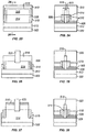
- Figure 1 is a cross-sectional side view diagram of a current flow control gate in FinFET architectures. It shows a portion of a fin on a substrate in a FinFET architecture.
- the fin 106, 108 protrudes from the substrate 102 which is covered in an isolation oxide 104.
- a device 101 is built on the substrate 102 and the fin.
- An n-well 106 is formed on the fin and may extend partially into the substrate and a p-type channel 108 has been formed over the n-well on the fin.
- the fin as shown is made up of these two parts, however, the fin may extend beyond the device and beyond the n-well and the p-channel on either side of the device.
- a pair of contacts 110, 112 is formed in the p-channel, one on each side of the channel.
- a control gate 114 is formed between the two contacts over the fin. Current flow from one channel contact 110 to the other channel contact 112 through the p-channel 108 is controlled by the control gate 114.
- FIG. 1 A part of the device 101 of Figure 1 is shown in the cross-sectional front view diagram of Figure 2 . This view is taken as a cross-section through the control gate 114, through the line 2-2 of Figure 1 . As shown, the isolation oxide 102 and the n-well 106 are directly over the substrate 102. The p-channel 108 is formed over the n-well 106.
- the control gate 114 is formed over and around the p-channel surrounding it on three sides. This allows the control gate to electrically pinch carrier flow through the p-channel between the two contacts 110, 112.
- the p-channel is surrounded by a barrier layer 118 between the p-channel and the control gate to prevent diffusion between the p-channel and the gate.
- the n-well extends through the isolation oxide.
- the n-well also extends above and below the top of the isolation oxide 104. This allows the control gate to extend all the way around the p-channel to more effectively control carrier flow through the p-channel. As shown, the control gate extends deeper on the fin than does the p-channel. This ensures that the p-channel is more than completely enclosed on three sides. Alternatively, the gate may be made smaller to allow a leakage current through the p-channel even when the maximum voltage has been applied to the control gate,
- Figure 3 is a cross-sectional front view diagram of the fin and device 101 of Figure 1 taken through either one of the two contacts 110, 112 and in this example through line 3-3 of Figure 1 .
- the n- well is deep through the isolation oxide 104 to the substrate 102.
- the contact is formed over the p-channel 108 to provide a suitable connection from an external source to the p-channel.
- the contact does not extend over the n-well and is not as deep as the control gate 114, Electrodes 120 and 122 are formed on the two contacts 110, 112 so that a current may be applied to one or the other of the two contacts. The current flow between the two contacts is then controlled by the control gate.
- Figure 4 is a cross-sectional front view diagram of an alternative contact 110-1.
- Figure 4 presents the same view as Figure 3 but for an alternative embodiment.
- the contact of Figure 4 may be formed by adding an isolation oxide 124 to the contact of Figure 3 .
- the same isolation oxide 104 and n-well 106 are formed over a substrate 102 such as a silicon substrate.
- the p-channel 108 is built over the n-well 106 and the top is covered with a contact 110, 126, similar to the contact 110 of Figure 3 .
- an additional fin spacer 124 is applied between the isolation oxide and the contact 126 to prevent diffusion from between the n-well and the p-type contact.
- the fin is first formed and then doped to form an n-well and p-channel.
- the fin spacer 124 is then built up around the fin with the doped contact 126 over it.
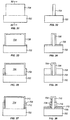
- Figure 5 is a cross-sectional side view diagram of an n-channel variable current How device in FinFET architecture. It shows an alternative variable resistor device 200 in which an n-channel is used instead of a p-channel. In this example no substrate is shown for simplicity, however, the device is formed using a FinFET architecture similar to the device of Figure 1 .
- a fin is built up over the substrate. The fin is doped to form a deep p-well 206. The fin is surrounded by an isolation oxide 204, The upper part of the fin is doped to form art n-channel 208 above the p-well 206.
- a pair of contacts in this case n-type contacts 210, 222, is formed one contact on either side of the n-channel. Electrodes 220, 224 are attached to the contacts to allow a current to be applied to one of the contacts.
- Flow through the n-channel 208 is controlled by a control gate 214 which has an electrode 230 to which a variable voltage may be applied.
- the variable resistor 200 of Figure 2 operates similarly to the variable resistor 101 of Figure 1 .
- An increasing voltage applied to the terminal 230 allows more current to flow through the n-channel by the control gate 214. In this case, the current is in the form of electrons rather than holes, however, the fundamental operation is the same.
- Figure 6 is a cross-sectional side view diagram of a p-channel device with variable current flow controlled by multiple gates in FinFET architecture.
- P-type contacts 310, 312 as in Figure 2 are combined with an n-type contact 318 to make a double gated p-type device 300.
- This device has a fin with a deep n-well 306. The upper part of the fin is doped as a p-channel 308 and the fin is surrounded by an isolation oxide 304.
- P-type contacts 310, 312 are formed at either end of the p-channel.
- An n-type contact 318 is formed between the two p-type channels.
- a first control gate 314 is placed between the left side p-type contact 310 and the center n-type contact 318.
- a second control gate 316 is placed between the n-type contact 318 and the right side p-type contact 312.
- the three contacts 310, 312, 318 each have a terminal 320, 324, 322 to which a current may be applied.
- the two control gates 314, 316 also have terminals 326, 328 to which a voltage may he applied.
- the current flow through the p-channel may be regulated.
- the n-type contact 318 may also be used to regulate current flow through the device 300. This three contact device allows for a very precise control of current flow which may be used for any of a variety of different purposes.
- a variety of different devices may be formed using a fin architecture and solid surface annealing.
- the most simple device has a contact at each end of a current channel.
- the contacts can be coupled to an electrode or another device. This supplies an isolated electrical conduit between two points.
- the structure can he augmented by one or more control gates as shown in Figures 1 and 6 .
- the structure can be augmented with transistor gates as shown in Figure 29 or the device may have a combination of different types of gates.
- a variety of different types of transistor, resistor, and other current control devices can be formed using the techniques described herein.
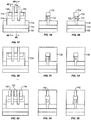
- Figures 7-28 are cross-sectional side view diagrams and corresponding front view diagrams of stages of fabrication for a variable resistor described, for example, in Figures 1 and 5 ,
- a substrate 402 such as a silicon substrate has been processed so that it has a fin 404 while only one fin is shown, typically a substrate will have many hundreds of fins or thousands depending upon the intended application.
- n doped glass is deposited over the substrate.
- the n-type glass 406 contains a doped oxide and may be in the form, for example, of a phosphosilicate.
- the glass may be applied by chemical vapor deposition or a variety of other processes.
- Figures 11 and 12 show that a spin-on hard mask 408 has been applied over the substrate and the glass as a thick blanket coat.
- the mask covers the substrate and a lower part of the fin.
- the mask layer leaves only the upper part of the fin exposed.
- the glass on the rest of the structure is covered.
- the spin-on hard mask has been used to protect the n-doped glass on the lower part of the fin and the substrate from an etch process.
- the n-doped glass applied to the top of the fin has been removed.
- the exposed top of the fin sets the depth of the p-type channel which is to be formed and also sets the back gate depth.
- the glass over the upper part of the fin has been removed the carbon hard mask has been removed and a low doped p-type glass has been deposited over the entire structure.
- Figures 15 and 16 the structure of Figures 13 and 14 has been annealed and all of the glass has then been removed.
- the anneal drives the dopants from the glass into the silicon or other thin material.
- the glass can then be removed using a standard oxide etching process or any of a variety of other processes.
- the structure of Figures 15 and 16 has a lower silicon portion 402 with an n-type substrate area 412 and an n-type lower portion of the fin 414.
- upper part of the substrate closest to the fin is also doped due to the n-type glass that was deposited over the substrate. This allows a very deep n-well to be formed under the p-channel at the top part of the fin.
- the top of the fin 416 is doped as p-type to later form a p-channel over a deep n-well.
- the doped glass forms a solid source of dopants.
- the dopants are diffused into the fin from the solid source when the structure is annealed.
- the particular process parameters of this solid source diffusion may be adjusted to suit the particular materials, the desired doping levels, and the overall process flow for fabricating the devices. While doped glass is described other solid source diffusion methods and technologies may be used depending on the particular application and process parameters.
- this isolation oxide may be any of a variety of oxides including silicon dioxide.
- the oxide is then planarized in Figures 19 and 20 and patterned to allow a polysilicon control gate 420 structure to be applied over the fin.
- the polysilicon material may then be removed and backfilled with metal to form a metal control gate.
- contacts 420, 422 are applied over the fin and a spacer 426 is applied to separate the control gate 420 from the two contacts 422, 424.
- the spacers may be formed by deposition and may be left in place to control epitaxial growth which may be applied to the structure in a later process.
- the control gate surrounds the fin on three sides, the top and two vertical sides of the fin.
- the contacts 420, 422 also surround the fin on the top and both sides.
- Figures 23 to 28 are side cross-sectional and corresponding front view diagrams of a stage of fabrication to show an alternative fabrication process.
- a deposition oxide has been applied over the structure of Figure 4G .
- the structure of 4G has been formed and this structure has then been annealed.
- an oxide isolation layer 518 is applied over the tin, the substrate and the glass.
- a portion 532 of the silicon substrate 502 is n-doped
- a portion of the fin 514 and the substrate 512 forms the deep n-well with a more highly doped p-type channel 556 on the upper part of the fin.
- the p-doped glass 510 covers the fin and the n-type glass 506 covers the fin and the substrate.
- the deposited oxide 518 has been planarized and removed down to below the n-well area or the start of the n-type portion of the fin 514. This exposes most of the fin. All of the deposited glass above the oxide layer 518 is then removed and a polysilicon structure 520 is formed over and around the fin to start the fabrication of the control gate.
- Figure 29 is a cross-sectional side view diagram of a transistor device formed on a fin of a FinFET architecture.
- solid-source diffusion may be used along with implantation to form contacts for a resistor.
- the same techniques may be used for the source 612, drain 614, and top back-gate contacts 626, 628 of a JFET.
- the p-channel, the source, gate and drain are all formed in a fin 622 of a FinFET device architecture.
- the n-type gate has a contact 624 that is also coupled to an n-type top gate 626 and a back gate 628 that are also formed on the fin electrically coupled to the p-channel but spaced apart from the source, gate, and drain.
- the n-type back 626 and top 620 gates deplete the narrow p-channel of carriers in between the source and the drain. This pinches off the channel and reduces the current that can flow from the source to the drain.
- a similar design may be applied to an n-type channel in a fin with an n-type source and drain and a p-type gate.
- control gates 630, 632 similar to the control gate of the variable resistor described herein may be used to further enhance or retard current flow through the p-channel.
- the control gates may be formed inside the JFET on one or both sides of the gate. Similar to the variable resistor of Figure 1 , the control gates of Figure 29 are fabricated over the fin covering the fin on the top and on two sides to substantially surround the p-channel.
- the three sided enclosure of the gate enables excellent electrostatic control of the carrier density inside the fin.
- the control gate is able to alternately increase the carrier density through channel accumulation and decrease the carrier density though channel depletion depending on the bias applied.
- the control gates are acting as a variable resistor built in to the fin-based JFET architecture. As JFETs are typically longer channel devices to sustain high voltage operation, these control gates typically have no added layout area penalty and improve the pinch-off voltage needed to fully shut off the channel.
- Figure 30 shows a corresponding circuit representation of the FinFET transistor showing the gate 620 to control current flow from the source 612 to the drain 614 and connections for the two control gates 630, 632.
- Standard processing is used to define the fins, and an n-type glass is subsequently deposited on top of the fins conformally.
- the glass is patterned using, for example a spin-on hard mask recessed to expose the top of the fins.
- a conformal p-type glass is then deposited.
- An anneal is performed to drive in the dopants from the glass into the silicon fins, and the glass is subsequently removed.
- Standard isolation oxide is deposited, planarized, and recessed to set the active fin height. The midsection gate spacers are then deposited.
- the spacer is completely or partially left on the fin to enable downstream epitaxial patterning of the JFET device.
- Epitaxial silicon undercut etch and growth may then be performed using conventional techniques and the gate isolation oxide may then be deposited to enable contact formation.
- the contacts for the source, drain, and gates are then constructed.
- Figures 31 -55 are cross-sectional side and front view diagrams of stages of fabrication of a JFET in a FinFET architecture.
- a substrate 702 has one or more fins 704 formed on it.
- the fin may be formed in any of a variety of different ways depending on the particular implementation.
- an n-type glass 706 is deposited over the fin and substrate. This glass may be formed by a variety of different deposition processes and contains a moderate dopant concentration of n-type dopant.
- borosilicate or phosphosilicate may be applied by chemical vapor deposition or any other technique may be used.
- a blocking material 708, such as a planarizing spin-on hard mask is applied and patterned over the substrate.
- a thick blanket is used so that the top of the fin is exposed while the bottom of the fin and the top of the substrate are coated.
- the height of the mask layer determines the depth of the p-channel.
- Figures 37 and 38 the n-type glass has been removed where it is exposed, that is where it is not covered by the spin-on hard mask, and after the glass has been etched away the blocking material is also removed. A highly concentrated p-type doped glass is then applied over the entire fin and substrate. The p-type glass 710 will allow the fin to be doped as a p-type material to build the p-channel.
- the substrate, fin, and glass have been annealed. This drives dopants in from the glass into the silicon material. The glass is then removed using, for example, an oxide etch to leave the structure shown in Figures 39 and 40 .
- This structure has a silicon substrate at its base and an n-doped well at the top of the substrate 712.
- the fin has a lower portion 714 that is also n-doped to form the back gate.
- the fin has an upper portion 716 which is p-doped to form the current flow channel.
- the entire structure is covered with an oxide layer 718, such as silicon dioxide or another oxide.
- the oxide forms an isolation oxide which is then planarized to a determined level as shown in Figures 43 and 44 to expose a certain portion of the fin.
- the oxide is removed away to expose a portion of the part of the fin that is n-doped 714.
- the fin is exposed so that the entire p-channel is exposed as is a portion of the N doped hack gate 714.
- a control gate 720 may then be formed around the entire exposed area of the fin down to the level of the oxide.
- the height or level of the oxide accordingly determines the size of the control gate.
- the control gate is deeper than the p-channel and covers the entire active fin height.
- control gates are typically metal and may be formed in any of a variety of different ways.
- the control gates are formed first by polysilicon patterning to build a structure corresponding to the desired shape 720 of the control gates. After the patterning is completed at this level the polysilicon is then removed leaving a void in the shape of the desired control gate. The void is then back filled with metal to form the control gate. Electrodes and other connectors may then be attached to the metal.
- a residual spacer has beers applied to the fin to control subsequent epitaxial growth.
- the spacer 722 is applied around the base of the fin over the oxide layer which remains in place.
- Figures 47 to 55 are cross-sectional side and front view diagrams of stages of further fabrication of the device of Figure 29 .
- source, gate, and drain are added.
- the cross-sectional front view of Figures 48, 51, and 54 are taken at the position of the source which is similar to the view at the drain.
- the front cross-sectional view of Figures 49, 52, and 55 are taken at the position of the gate, rather than at the position of the control gate as in Figures 31 to 46 . This is because the control gates, at least in polysilicon form have already been formed and are not affected by the other stages,
- the source gate and drain of the JFET have been formed.
- the source 730 and drain 732 are formed by epitaxial growth of a p-type element and the gate 734 is formed by n-type epitaxial growth.
- the source and drain are formed over the fin and the spacer using patterning and epitaxial growth.
- the source and drain are prevented by the spacer 722 from corning into contact with or coming too close to the deep n-well or back gate 714 of the fin.
- each contact node makes contact only with the p-channel.
- the source and drain can be formed by applying a doped material over the p-channel or by doping the actual p-channel.
- the n-type gate is formed in the fin or over the fin and is blocked by the. fin spacer 722 from coming too close to the n-type back gate.
- the control gate wraps all the way around the p-channel and is physically contacting the n-type back gate.
- a first control gate is between and in contact with the source and the gate and the second control gate is between and in contact with the gate and the drain.
- an isolation barrier is applied over and surrounding the control gates to prevent conduction and electrical contact between the control gates and the source, gate, and drain.
- the control gates may be isolated with any of variety of dielectric barriers and may also be physically spaced apart from any other structure.
- the entire structure is covered in a deep layer of isolation oxide 738 this isolates the source, gate, and drain as well as the control gates from each other.
- the top layer of the isolation oxide may be planarized using any of a variety of different processes to be, for example, at the level of the top of the control gates, electrodes and other structures.
- the fin, together with the source, gate, and drain are well below the isolation oxide in this example.
- contacts are formed over the gates, these contacts 740, 742 and 744 allow connections to be made to the source, gate, and drain of the transistor device.
- the polysilicon control gates may be dissolved and backfilled with metal depending upon the particular implementation for the control gates.
- the top layer of dielectric 738 may be used as an interlayer dielectric in the event that additional components are to be formed over the JFET structure.
- the electrodes may be formed of any of a variety of different materials depending on the fabrication technology including tungsten.
- JFET transistor type
- SoC SoC
- power application or other type of IC that is fabricated using a non-planar transistor process technology.
- resistor or JFET device provides unique FinFET transport characteristics that are not seen in a planar fabrication technology.
- Figure 55 illustrates a competing device 100 in accordance with one implementation of the invention.
- the computing device 100 houses a system board 2.
- the board 2 may include a number of components, including but not limited to a processor 4 and at least one communication package 6.
- the communication package is coupled to one or more antennas 16.
- the processor 4 is physically and electrically coupled to the board 2.
- any one or more of the components, controllers, hubs, or interfaces are constructed using a FinFET architecture that includes solid source-diffused junctions.
- computing device 100 may include other components that may or may not be physically and electrically coupled to the board 2.
- these other components include, but are not limited to, volatile memory (e.g., DRAM) 8, non-volatile memory (e.g., ROM) 9, flash memory (not shown), a graphics processor 12, a digital signal processor (not shown), a crypto processor (not shown), a chipset 14, an antenna 16, a display 18 such as a touchscreen display, a touchscreen controller 20, a battery 22, an audio codec (not shown), a video codec (not shown), a power amplifier 24, a global positioning system (GPS) device 26, a compass 28, an accelerometer (not shown), a gyroscope (not shown), a speaker 30, a camera 32, and a mass storage device (such as hard disk drive) 10, compact disk (CD) (not shown), digital versatile disk (DVD) (not shown), and so forth).
- volatile memory e.g., DRAM
- non-volatile memory e.g., ROM
- the communication package 6 enables wireless and/or wired communications for the transfer of data to and from the computing device 100.
- wireless and its derivatives may be used to describe circuits, devices, systems, methods, techniques, communications channels, etc., that may communicate data through the use of modulated electromagnetic radiation through a non-solid medium. The term does not imply that the associated devices do not contain any wires, although in some embodiments they might not.
- the communication package 6 may implement any of a number of wireless or wired standards or protocols, including but not limited to Wi-Fi (IEEE 802.11 family), WiMAX (IEEE 802.16 family), IEEE 802.20, long term evolution (LTE), Ev-DG, HSPA+, HSDPA+, HSUPA+, EDGE, GSM, GPRS, CDMA, TDMA, DECT, Bluetooth, Ethernet derivatives thereof, as well as any other wireless and wired protocols that are designated as 3G, 4G, 5G, and beyond,
- the computing device 100 may include a plurality of communication packages 6, For instance, a first communication package 6 may be dedicated to shorter range wireless communications such as Wi-Fi and Bluetooth and a second communication package 6 may be dedicated to longer range wireless communications such as GPS, EDGE, GPRS, CDMA, WiMAX, LTE, Ev-DO, and others.
- the processor 4 of the computing device 100 includes an integrated circuit die packaged within the processor 4.
- the term "processor” may refer to any device or portion of a device that processes electronic data from registers and/or memory to transform that electronic data into other electronic data that may be stored in registers and/or memory.
- the computing device 100 may be a laptop, a netbook, a notebook, an ultrabook, a smartphone, a tablet, a personal digital assistant (PDA), an ultra mobile PC, a mobile phone, a desktop computer, a server, a printer, a scanner, a monitor, a settop box, an entertainment control unit, a digital camera, a portable music player, or a digital video recorder.
- the computing device may be fixed, portable, or wearable, in further implementations, the computing device 100 may be any other electronic device that processes data.
- Embodiments may be implemented as a part of one or more memory chips, controllers, CPUs (Central Processing Unit), microchips or integrated circuits interconnected using a motherboard, an application specific integrated circuit (ASIC), and/or a field programmable gate array (FPGA).
- CPUs Central Processing Unit
- ASIC application specific integrated circuit
- FPGA field programmable gate array
- references to “one embodiment”, “an embodiment”, “example embodiment”, “various embodiments”, etc., indicate that the embodiment(s) of the invention so described may include particular features, structures, or characteristics, but not every embodiment necessarily includes the particular features, structures, or characteristics. Further, some embodiments may have some, all, or none of the features described for other embodiments.
- Coupled is used to indicate that two or more elements co-operate or interact with each other, but they may or may not have intervening physical or electrical components between them.
- Some embodiments pertain to a method including forming a fin on a substrate, depositing a glass of a first dopant type over the substrate and over a lower portion of the fin, depositing a glass of a second dopant type over the substrate and the fin, annealing the glass to drive the dopants into the fin and the substrate, removing the glass, and forming a first and a second contact over the fin without contacting the lower portion of the fin.
- control gate is a conductive material over the top and on the sides of the fin to control current flow through the fin between the first and second contacts.
- forming a control gate comprises patterning polysilicon over the fin, removing the polysilicon and backfilling the void front the polysilicon with metal.
- Forming a control gate comprises forming a control gate over the fin after removing the glass and before forming the first and second contacts.
- the first contact comprises a source
- the second contact comprises a drain
- the method further comprising forming a gate over the fin between the source and the drain without contacting the lower portion of the fin.
- Further embodiments include depositing art oxide over the silicon substrate after removing the glass, the oxide having a depth to cover the lower portion of the fin, the oxide isolating the lower portion of the fin before forming the doped source, gate, and drain.
- Further embodiments include forming an isolation spacer over the lower portion of the fin before forming the source, gate, and drain to prevent the source, gate, and drain from contacting the lower portion of the fin.
- the substrate and the fin are silicon.
- depositing a glass of a first dopant type includes depositing the glass of the first dopant type over the substrate and the fin, depositing a blocking material (carbon hard mask) over the substrate and a portion of the fin, removing the deposited glass that is not covered in the blocking material, and removing the blocking material.
- a blocking material carbon hard mask
- the blocking material is n carbon hard mask.
- Depositing glass of a second dopant type comprises removing the glass of the first dopant type from a portion of the fin and depositing the glass of the second dopant type over the portion of the fin and over the glass of the first dopant type.
- Removing the glass comprises removing the glass using an oxide etcher.
- control gate is a conductive material over the top and on the sides of the fin to control current flow through the fin between the source and the drain.
- forming a control gate comprises patterning polysilicon over the fin, removing the polysilicon and backfilling the void from the polysilicon with metal.
- Forming a control gate comprises forming a control gate over the fin after removing the glass and before forming the source, gate, and drain.
- Some embodiments pertain to an apparatus including a substrate, a fin above the substrate, the fin having a channel of a first dopant type and at least a portion of a well of a second dopant type, and a first contact and a second contact of the fin formed without contacting the well of the fin;
- control gate between the first and second contact formed over and around the fin to control resistance between the first and the second contact.
- control gate is metal.
- the control gale is formed of polysilicon which is then removed and a void caused by removing the polysilicon is filled with metal.
- the first and the second contacts are formed of the first dopant type.
- the first and second contacts are formed over the fin of epitaxial growth.
- the first and second contacts are formed in the fin of a dopant in the fin.
- the channel of the first dopant type is a current channel between the first and second contacts.
- the control gate extends over and around the channel of the fin on two sides.
- the first contact comprises a source and the second contact comprises a drain
- the apparatus further comprising a gate of the second dopant type formed of the fin between the source and the drain formed without contacting the well of the fin.
- the gate is formed over the fin of epitaxial growth.
- the gate is formed in the fin of a dopant in the fin.
- the gate is formed in the fin by depositing a doped glass over the fin, annealing the glass, and removing the glass.
- the channel of the first dopant type is a current channel between the source and the drain and wherein a voltage applied to the gate determines whether current flows in the channel.
- control gate between the source and the drain, the control gate extending over and around the channel of the fin on two sides and being configured to restrict current flow through the channel.
- control gate is between the source and the gate, the transistor further composing a second control gate between the gate and the drain.
- the control gate is metal.
- the control gate is formed of polysilicon which is then removed and a void caused by removing the polysilicon is filled with metal.
- Some embodiments pertain to a computing system including a communication chip, a power supply and a processor having a plurality of transistors, at least one transistor being a junction gate field effect transistor having a substrate, a fin above the substrate, the fin having a channel of a first dopant type and at least a portion of a well of a second dopant type, a source and a drain of the first dopant type of the fin formed without contacting the well of the fin, and a gate of the second dopant type formed of the fin between the source and the drain formed without contacting the well of the fin.
- the gate is formed in the fin by depositing a doped glass over the fin, annealing the glass, and removing the glass.
- the junction gate field effect transistor further includes a control gate between the source and the gate, the control gate being formed over and around the fin to control resistance between the source and the drain.
- the control gate is formed by patterning polysilicon over the fin, removing the polysilicon and backfilling the void from the polysilicon with metal
- Some embodiments pertain to a junction gate field effect transistor including a substrate, a fin above the substrate, the fin having a channel of a first dopant type and at least a portion of a well of a second dopant type, a source and a drain of the first dopant type of die fin formed without contacting the well of the fin, and a gate of the second dopant type formed of the fin between the source and the drain formed without contacting the well of the fin.
- variable resistor including a substrate, a fin above, the substrate, the fin having a channel of a first dopant type and at least a portion of a well of a second dopant type, a first contact and a second contact of the fin formed without contacting the well of the fin, and a control gate between the first and second contact formed over and around the fin to control resistance between the first and the second contact.
Abstract
Description
- The present disclosure relates to Fin-based electronics and, in particular to junctions using solid source diffusion.
- Monolithic integrated circuits typically have a large number of transistors, such as metal-oxide semiconductor field-effect transistors (MOSFETs) fabricated over a planar substrate, such as a silicon wafer. System-on-a-chip (SoC) architectures use such transistors in both analog and digital circuitry. When high-speed analog circuitry is integrated on a single monolithic structure with digital circuitry, the digital switching can induce substrate, noise that limits the precision and linearity of the analog circuitry.
- Junction gate field effect transistors (JFETs) are used primarily in analog applications due to the superior low noise performance they offer compared to standard MOSFET (Metal Oxide Semiconductor FET) devices, JFETs are useful in radio frequency devices such as filters and equalizers and also in power circuits for power supplies, power conditioners and the like.
- JFET transistors are fabricated in the bulk of a planar process technology using implanted junctions to establish a back-gate, channel, and top-gate electrodes. The JFET is made using implanted n and p-type wells to form the top and back gates, as well as the source and drain contacts. This bulk planar process may be replaced for MOSFET devices using fins formed on the substrate. The formation of FET devices on fins has been referred to as a FinFET architecture.
- Embodiments of the invention are illustrated by way of example, and not by way of limitation, in the figures of the accompanying drawings in which like reference numerals refer to similar elements.
-
Figures 1-4 are cross-sectional side view and corresponding front view diagrams of a p-channel current flow control gate on a fin architecture according to an embodiment of the invention. -
Figure 5 is a cross-sectional side view diagram of an n-channel current flow control gate on fin architecture according to an embodiment of the invention. -
Figure 6 is a cross-sectional side view diagram of a p-channel current flow control device with multiple gates on fin architecture according to an embodiment of the invention. -
Figures 7-22 are cross-sectional side view and corresponding front view diagrams of stages of fabrication for the device ofFigure 1 according to an embodiment of the invention. -
Figures 23-28 are cross-sectional side view and corresponding front view diagrams of alternative stages of fabrication forFigures 13-22 according to an embodiment of the invention. -
Figure 29 is a cross-sectional side view diagram of a transistor on a FinFET architecture according to an embodiment of the invention. -
Figure 30 is a circuit diagram of the transistor ofFigure 29 according to an embodiment of the invention. -
Figures 31-55 are cross-sectional side view and corresponding front view diagrams of alternative stages of fabrication of the transistor ofFigure 29 according to an embodiment of the invention. -
Figure 56 is a block diagram of a computing device incorporating an integrated circuit built with a FinFET architecture and including a solid source diffused junction according to an embodiment. - A high performance JFET may be fabricated on a fin of a FinFET process architecture, Because the electrical characteristics of a JFET rely on its structure as a bulk-transport device, a JFET device built on a fin in the same way as a MOSFET device loses its bulk transport and high current capabilities, A JFET can be built, however, using solid-source diffusion on a fin architecture to obtain a high-performance, scalable device for system-on-chip process technologies.
- A similar technique may be used to form a variable resistor. A p-channel or n-channel may be formed in a fin with a contact on either side. A control gate may be formed over the channel in the fin between the two contacts. Due to the nature of current conduction inside of the fin and the narrow width of the fin, the control gate provides excellent electrostatic control of the carrier density inside the fin. By using this control gate, the carrier density can be increased (through channel accumulation) or decreased (though channel depletion) depending on the bias applied.
- The same control gate technique may also be used on one or both sides of the gate of a JFET in a fin. The control gates act as a variable resistor bulk into the fin-based JFET architecture. As JFETs are typically longer channel devices lo sustain high voltage operation, these control gates have no added layout area penalty and may improve the pinch-off voltage needed to fully shut off the channel.
-
Figure 1 is a cross-sectional side view diagram of a current flow control gate in FinFET architectures. It shows a portion of a fin on a substrate in a FinFET architecture. Thefin substrate 102 which is covered in anisolation oxide 104. Adevice 101 is built on thesubstrate 102 and the fin. An n-well 106 is formed on the fin and may extend partially into the substrate and a p-type channel 108 has been formed over the n-well on the fin. The fin as shown is made up of these two parts, however, the fin may extend beyond the device and beyond the n-well and the p-channel on either side of the device. A pair ofcontacts control gate 114 is formed between the two contacts over the fin. Current flow from onechannel contact 110 to the other channel contact 112 through the p-channel 108 is controlled by thecontrol gate 114. - A part of the
device 101 ofFigure 1 is shown in the cross-sectional front view diagram ofFigure 2 . This view is taken as a cross-section through thecontrol gate 114, through the line 2-2 ofFigure 1 . As shown, theisolation oxide 102 and the n-well 106 are directly over thesubstrate 102. The p-channel 108 is formed over the n-well 106. - The
control gate 114 is formed over and around the p-channel surrounding it on three sides. This allows the control gate to electrically pinch carrier flow through the p-channel between the twocontacts barrier layer 118 between the p-channel and the control gate to prevent diffusion between the p-channel and the gate. - The n-well extends through the isolation oxide. The n-well also extends above and below the top of the
isolation oxide 104. This allows the control gate to extend all the way around the p-channel to more effectively control carrier flow through the p-channel. As shown, the control gate extends deeper on the fin than does the p-channel. This ensures that the p-channel is more than completely enclosed on three sides. Alternatively, the gate may be made smaller to allow a leakage current through the p-channel even when the maximum voltage has been applied to the control gate, -
Figure 3 is a cross-sectional front view diagram of the fin anddevice 101 ofFigure 1 taken through either one of the twocontacts Figure 1 . As shown, the n- well is deep through theisolation oxide 104 to thesubstrate 102. The contact is formed over the p-channel 108 to provide a suitable connection from an external source to the p-channel. The contact does not extend over the n-well and is not as deep as thecontrol gate 114, Electrodes 120 and 122 are formed on the twocontacts -
Figure 4 is a cross-sectional front view diagram of an alternative contact 110-1.Figure 4 presents the same view asFigure 3 but for an alternative embodiment. The contact ofFigure 4 may be formed by adding anisolation oxide 124 to the contact ofFigure 3 . Thesame isolation oxide 104 and n-well 106 are formed over asubstrate 102 such as a silicon substrate. The p-channel 108 is built over the n-well 106 and the top is covered with acontact contact 110 ofFigure 3 . In the example ofFigure 4 an additionalfin spacer 124 is applied between the isolation oxide and thecontact 126 to prevent diffusion from between the n-well and the p-type contact. In practice, the fin is first formed and then doped to form an n-well and p-channel. Thefin spacer 124 is then built up around the fin with thedoped contact 126 over it. -
Figure 5 is a cross-sectional side view diagram of an n-channel variable current How device in FinFET architecture. It shows an alternativevariable resistor device 200 in which an n-channel is used instead of a p-channel. In this example no substrate is shown for simplicity, however, the device is formed using a FinFET architecture similar to the device ofFigure 1 . A fin is built up over the substrate. The fin is doped to form a deep p-well 206. The fin is surrounded by anisolation oxide 204, The upper part of the fin is doped to form art n-channel 208 above the p-well 206. - A pair of contacts, in this case n-
type contacts Electrodes 220, 224 are attached to the contacts to allow a current to be applied to one of the contacts. Flow through the n-channel 208 is controlled by acontrol gate 214 which has anelectrode 230 to which a variable voltage may be applied. Thevariable resistor 200 ofFigure 2 operates similarly to thevariable resistor 101 ofFigure 1 . An increasing voltage applied to the terminal 230 allows more current to flow through the n-channel by thecontrol gate 214. In this case, the current is in the form of electrons rather than holes, however, the fundamental operation is the same. -
Figure 6 is a cross-sectional side view diagram of a p-channel device with variable current flow controlled by multiple gates in FinFET architecture. P-type contacts Figure 2 are combined with an n-type contact 318 to make a double gated p-type device 300. This device has a fin with a deep n-well 306. The upper part of the fin is doped as a p-channel 308 and the fin is surrounded by anisolation oxide 304. P-type contacts type contact 318 is formed between the two p-type channels. Afirst control gate 314 is placed between the left side p-type contact 310 and the center n-type contact 318. Asecond control gate 316 is placed between the n-type contact 318 and the right side p-type contact 312. The threecontacts control gates terminals type contact 318 may also be used to regulate current flow through thedevice 300. This three contact device allows for a very precise control of current flow which may be used for any of a variety of different purposes. - As shown in
Figures 1 -6 , a variety of different devices may be formed using a fin architecture and solid surface annealing. The most simple device has a contact at each end of a current channel. The contacts can be coupled to an electrode or another device. This supplies an isolated electrical conduit between two points. The structure can he augmented by one or more control gates as shown inFigures 1 and6 . The structure can be augmented with transistor gates as shown inFigure 29 or the device may have a combination of different types of gates. A variety of different types of transistor, resistor, and other current control devices can be formed using the techniques described herein. -
Figures 7-28 are cross-sectional side view diagrams and corresponding front view diagrams of stages of fabrication for a variable resistor described, for example, inFigures 1 and5 , InFigures 7 and 8 asubstrate 402 such as a silicon substrate has been processed so that it has afin 404 while only one fin is shown, typically a substrate will have many hundreds of fins or thousands depending upon the intended application. - In
Figures 9 and 10 an n doped glass is deposited over the substrate. The n-type glass 406 contains a doped oxide and may be in the form, for example, of a phosphosilicate. The glass may be applied by chemical vapor deposition or a variety of other processes. -
Figures 11 and 12 show that a spin-onhard mask 408 has been applied over the substrate and the glass as a thick blanket coat. The mask covers the substrate and a lower part of the fin. The mask layer leaves only the upper part of the fin exposed. The glass on the rest of the structure is covered. A blanket coat of such a blocking material, by protecting some areas and not others, allows additional layers lo be applied selectively. - In this case, as shown in
Figures 13 and 14 the spin-on hard mask has been used to protect the n-doped glass on the lower part of the fin and the substrate from an etch process. As a result, the n-doped glass applied to the top of the fin has been removed. As shown inFigures 13 and 14 , the exposed top of the fin sets the depth of the p-type channel which is to be formed and also sets the back gate depth. InFigures 13 and 14 the glass over the upper part of the fin has been removed the carbon hard mask has been removed and a low doped p-type glass has been deposited over the entire structure. - In
Figures 15 and 16 the structure ofFigures 13 and 14 has been annealed and all of the glass has then been removed. The anneal drives the dopants from the glass into the silicon or other thin material. The glass can then be removed using a standard oxide etching process or any of a variety of other processes. As a result of the glass deposition and annealing, the structure ofFigures 15 and 16 has alower silicon portion 402 with an n-type substrate area 412 and an n-type lower portion of thefin 414. Note that upper part of the substrate closest to the fin is also doped due to the n-type glass that was deposited over the substrate. This allows a very deep n-well to be formed under the p-channel at the top part of the fin. The top of thefin 416 is doped as p-type to later form a p-channel over a deep n-well. - In this example, the doped glass forms a solid source of dopants. The dopants are diffused into the fin from the solid source when the structure is annealed. The particular process parameters of this solid source diffusion may be adjusted to suit the particular materials, the desired doping levels, and the overall process flow for fabricating the devices. While doped glass is described other solid source diffusion methods and technologies may be used depending on the particular application and process parameters.
- In
Figures 17 and 18 anisolation oxide 418 is applied, this isolation oxide may be any of a variety of oxides including silicon dioxide. The oxide is then planarized inFigures 19 and 20 and patterned to allow apolysilicon control gate 420 structure to be applied over the fin. The polysilicon material may then be removed and backfilled with metal to form a metal control gate. - In
Figures 21 and 22 ,contacts control gate 420 from the twocontacts - As shown in
Figures 19 and 20 , the control gate surrounds the fin on three sides, the top and two vertical sides of the fin. Similarly, thecontacts -
Figures 23 to 28 are side cross-sectional and corresponding front view diagrams of a stage of fabrication to show an alternative fabrication process. In the example ofFigures 23 and 24 , a deposition oxide has been applied over the structure ofFigure 4G . The structure of 4G has been formed and this structure has then been annealed. However, instead of then removing the doped glass from the structure, anoxide isolation layer 518 is applied over the tin, the substrate and the glass. As a result of the anneal, a portion 532 of thesilicon substrate 502 is n-doped, a portion of thefin 514 and thesubstrate 512 forms the deep n-well with a more highly doped p-type channel 556 on the upper part of the fin. Due to the oxide isolation structure, the p-dopedglass 510 covers the fin and the n-type glass 506 covers the fin and the substrate. - In
Figures 25 and 26 the depositedoxide 518 has been planarized and removed down to below the n-well area or the start of the n-type portion of thefin 514. This exposes most of the fin. All of the deposited glass above theoxide layer 518 is then removed and apolysilicon structure 520 is formed over and around the fin to start the fabrication of the control gate. - In
Figures 27 and 28 the control gate has been formed, the extra oxide has been removed, and the device is in a preliminary stage ready for application of the contacts as shown inFigures 21 and 22 . By applying the isolation oxide before removing the deposited glass layers, several steps in the fabrication process may be avoided, reducing costs. -
Figure 29 is a cross-sectional side view diagram of a transistor device formed on a fin of a FinFET architecture. As described above, solid-source diffusion may be used along with implantation to form contacts for a resistor. The same techniques may be used for thesource 612, drain 614, and topback-gate contacts JFET 600 as shown inFigure 29 , current flows from a p-type source 612 to a p-type drain 614 through, in this case, a p-type channel 636 when agate 620 between the source and drain is off. The p-channel, the source, gate and drain are all formed in afin 622 of a FinFET device architecture. The n-type gate has acontact 624 that is also coupled to an n-type top gate 626 and aback gate 628 that are also formed on the fin electrically coupled to the p-channel but spaced apart from the source, gate, and drain. - As the gate voltage is increased, the n-type back 626 and top 620 gates deplete the narrow p-channel of carriers in between the source and the drain. This pinches off the channel and reduces the current that can flow from the source to the drain. A similar design may be applied to an n-type channel in a fin with an n-type source and drain and a p-type gate.
- Using a fin-based architecture
additional control gates Figure 1 , the control gates ofFigure 29 are fabricated over the fin covering the fin on the top and on two sides to substantially surround the p-channel. - Due to the nature of current conduction inside of the fin and the narrow width of the fin, the three sided enclosure of the gate enables excellent electrostatic control of the carrier density inside the fin. The control gate is able to alternately increase the carrier density through channel accumulation and decrease the carrier density though channel depletion depending on the bias applied. As described above, in this way the control gates are acting as a variable resistor built in to the fin-based JFET architecture. As JFETs are typically longer channel devices to sustain high voltage operation, these control gates typically have no added layout area penalty and improve the pinch-off voltage needed to fully shut off the channel.
-
Figure 30 shows a corresponding circuit representation of the FinFET transistor showing thegate 620 to control current flow from thesource 612 to thedrain 614 and connections for the twocontrol gates - An example process sequence on a 14nm like technology is illustrated below. Standard processing is used to define the fins, and an n-type glass is subsequently deposited on top of the fins conformally. The glass is patterned using, for example a spin-on hard mask recessed to expose the top of the fins. A conformal p-type glass is then deposited. An anneal is performed to drive in the dopants from the glass into the silicon fins, and the glass is subsequently removed. Standard isolation oxide is deposited, planarized, and recessed to set the active fin height. The midsection gate spacers are then deposited.
- In some embodiments, the spacer is completely or partially left on the fin to enable downstream epitaxial patterning of the JFET device. Epitaxial silicon undercut etch and growth may then be performed using conventional techniques and the gate isolation oxide may then be deposited to enable contact formation. The contacts for the source, drain, and gates are then constructed.
-
Figures 31 -55 are cross-sectional side and front view diagrams of stages of fabrication of a JFET in a FinFET architecture. InFigures 31 and 32 asubstrate 702 has one ormore fins 704 formed on it. The fin may be formed in any of a variety of different ways depending on the particular implementation. InFigures 33 and 34 an n-type glass 706 is deposited over the fin and substrate. This glass may be formed by a variety of different deposition processes and contains a moderate dopant concentration of n-type dopant. As mentioned above borosilicate or phosphosilicate may be applied by chemical vapor deposition or any other technique may be used. - In
Figures 35 and 36 a blockingmaterial 708, such as a planarizing spin-on hard mask is applied and patterned over the substrate. In the illustrated example a thick blanket is used so that the top of the fin is exposed while the bottom of the fin and the top of the substrate are coated. The height of the mask layer determines the depth of the p-channel. - In
Figures 37 and 38 the n-type glass has been removed where it is exposed, that is where it is not covered by the spin-on hard mask, and after the glass has been etched away the blocking material is also removed. A highly concentrated p-type doped glass is then applied over the entire fin and substrate. The p-type glass 710 will allow the fin to be doped as a p-type material to build the p-channel. - In
Figures 39 and 40 the substrate, fin, and glass have been annealed. This drives dopants in from the glass into the silicon material. The glass is then removed using, for example, an oxide etch to leave the structure shown inFigures 39 and 40 . This structure has a silicon substrate at its base and an n-doped well at the top of thesubstrate 712. In addition, the fin has alower portion 714 that is also n-doped to form the back gate. The fin has anupper portion 716 which is p-doped to form the current flow channel. - In
Figures 41 and 42 the entire structure is covered with anoxide layer 718, such as silicon dioxide or another oxide. The oxide forms an isolation oxide which is then planarized to a determined level as shown inFigures 43 and 44 to expose a certain portion of the fin. The oxide is removed away to expose a portion of the part of the fin that is n-doped 714. As shown inFigures 43 and 44 the fin is exposed so that the entire p-channel is exposed as is a portion of the N dopedhack gate 714. Acontrol gate 720 may then be formed around the entire exposed area of the fin down to the level of the oxide. The height or level of the oxide accordingly determines the size of the control gate. The control gate is deeper than the p-channel and covers the entire active fin height. - The control gates are typically metal and may be formed in any of a variety of different ways. In the illustrated example, the control gates are formed first by polysilicon patterning to build a structure corresponding to the desired
shape 720 of the control gates. After the patterning is completed at this level the polysilicon is then removed leaving a void in the shape of the desired control gate. The void is then back filled with metal to form the control gate. Electrodes and other connectors may then be attached to the metal. In the illustrated example there are two control gates however there may be one or no control gates depending upon the intended final form of the JFET. - In
Figures 45 and 46 a residual spacer has beers applied to the fin to control subsequent epitaxial growth. Thespacer 722 is applied around the base of the fin over the oxide layer which remains in place. -
Figures 47 to 55 are cross-sectional side and front view diagrams of stages of further fabrication of the device ofFigure 29 . In these figures source, gate, and drain are added. The cross-sectional front view ofFigures 48, 51, and 54 are taken at the position of the source which is similar to the view at the drain. The front cross-sectional view ofFigures 49, 52, and 55 are taken at the position of the gate, rather than at the position of the control gate as inFigures 31 to 46 . This is because the control gates, at least in polysilicon form have already been formed and are not affected by the other stages, - In
Figures 47, 48, and 49 the source gate and drain of the JFET have been formed. Thesource 730 and drain 732 are formed by epitaxial growth of a p-type element and thegate 734 is formed by n-type epitaxial growth. The source and drain are formed over the fin and the spacer using patterning and epitaxial growth. The source and drain are prevented by thespacer 722 from corning into contact with or coming too close to the deep n-well or backgate 714 of the fin. As a result, each contact node makes contact only with the p-channel. The source and drain can be formed by applying a doped material over the p-channel or by doping the actual p-channel. Similarly, the n-type gate is formed in the fin or over the fin and is blocked by the.fin spacer 722 from coming too close to the n-type back gate. On the other hand, as shown inFigure 22 for example the control gate wraps all the way around the p-channel and is physically contacting the n-type back gate. - As illustrated a first control gate is between and in contact with the source and the gate and the second control gate is between and in contact with the gate and the drain. As shown, an isolation barrier is applied over and surrounding the control gates to prevent conduction and electrical contact between the control gates and the source, gate, and drain. The control gates may be isolated with any of variety of dielectric barriers and may also be physically spaced apart from any other structure.
- In
figures 50, 51, and 52 the entire structure is covered in a deep layer ofisolation oxide 738 this isolates the source, gate, and drain as well as the control gates from each other. The top layer of the isolation oxide may be planarized using any of a variety of different processes to be, for example, at the level of the top of the control gates, electrodes and other structures. The fin, together with the source, gate, and drain are well below the isolation oxide in this example. - In
Figures 53, 54, and 55 contacts are formed over the gates, thesecontacts dielectric 738 may be used as an interlayer dielectric in the event that additional components are to be formed over the JFET structure. The electrodes may be formed of any of a variety of different materials depending on the fabrication technology including tungsten. - As described, a very common and widely used transistor type (JFET) may be used in a SoC, power application, or other type of IC that is fabricated using a non-planar transistor process technology. Furthermore, the resistor or JFET device provides unique FinFET transport characteristics that are not seen in a planar fabrication technology.
-
Figure 55 illustrates a competingdevice 100 in accordance with one implementation of the invention. Thecomputing device 100 houses asystem board 2. Theboard 2 may include a number of components, including but not limited to aprocessor 4 and at least onecommunication package 6. The communication package is coupled to one ormore antennas 16. Theprocessor 4 is physically and electrically coupled to theboard 2. In some implementations of the invention, any one or more of the components, controllers, hubs, or interfaces are constructed using a FinFET architecture that includes solid source-diffused junctions. - Depending on its applications,
computing device 100 may include other components that may or may not be physically and electrically coupled to theboard 2. These other components include, but are not limited to, volatile memory (e.g., DRAM) 8, non-volatile memory (e.g., ROM) 9, flash memory (not shown), agraphics processor 12, a digital signal processor (not shown), a crypto processor (not shown), achipset 14, anantenna 16, adisplay 18 such as a touchscreen display, atouchscreen controller 20, abattery 22, an audio codec (not shown), a video codec (not shown), apower amplifier 24, a global positioning system (GPS)device 26, acompass 28, an accelerometer (not shown), a gyroscope (not shown), aspeaker 30, acamera 32, and a mass storage device (such as hard disk drive) 10, compact disk (CD) (not shown), digital versatile disk (DVD) (not shown), and so forth). These components may be connected to thesystem board 2, mounted to the system board, or combined with any of the other components. - The
communication package 6 enables wireless and/or wired communications for the transfer of data to and from thecomputing device 100. The term "wireless" and its derivatives may be used to describe circuits, devices, systems, methods, techniques, communications channels, etc., that may communicate data through the use of modulated electromagnetic radiation through a non-solid medium. The term does not imply that the associated devices do not contain any wires, although in some embodiments they might not. Thecommunication package 6 may implement any of a number of wireless or wired standards or protocols, including but not limited to Wi-Fi (IEEE 802.11 family), WiMAX (IEEE 802.16 family), IEEE 802.20, long term evolution (LTE), Ev-DG, HSPA+, HSDPA+, HSUPA+, EDGE, GSM, GPRS, CDMA, TDMA, DECT, Bluetooth, Ethernet derivatives thereof, as well as any other wireless and wired protocols that are designated as 3G, 4G, 5G, and beyond, Thecomputing device 100 may include a plurality ofcommunication packages 6, For instance, afirst communication package 6 may be dedicated to shorter range wireless communications such as Wi-Fi and Bluetooth and asecond communication package 6 may be dedicated to longer range wireless communications such as GPS, EDGE, GPRS, CDMA, WiMAX, LTE, Ev-DO, and others. - The
processor 4 of thecomputing device 100 includes an integrated circuit die packaged within theprocessor 4. The term "processor" may refer to any device or portion of a device that processes electronic data from registers and/or memory to transform that electronic data into other electronic data that may be stored in registers and/or memory. - In various implementations, the
computing device 100 may be a laptop, a netbook, a notebook, an ultrabook, a smartphone, a tablet, a personal digital assistant (PDA), an ultra mobile PC, a mobile phone, a desktop computer, a server, a printer, a scanner, a monitor, a settop box, an entertainment control unit, a digital camera, a portable music player, or a digital video recorder. The computing device may be fixed, portable, or wearable, in further implementations, thecomputing device 100 may be any other electronic device that processes data. - Embodiments may be implemented as a part of one or more memory chips, controllers, CPUs (Central Processing Unit), microchips or integrated circuits interconnected using a motherboard, an application specific integrated circuit (ASIC), and/or a field programmable gate array (FPGA).
- References to "one embodiment", "an embodiment", "example embodiment", "various embodiments", etc., indicate that the embodiment(s) of the invention so described may include particular features, structures, or characteristics, but not every embodiment necessarily includes the particular features, structures, or characteristics. Further, some embodiments may have some, all, or none of the features described for other embodiments.
- In the following description and claims, the term "coupled" along with its derivatives, may be used. "Coupled" is used to indicate that two or more elements co-operate or interact with each other, but they may or may not have intervening physical or electrical components between them.
- As used in the claims, unless otherwise specified, the use of the ordinal adjectives "first", "second", "third", etc., to describe a common element, merely indicate that different instances of like elements are being referred to, and are not intended to imply that the elements so described mast he in a givers sequence, either temporally, spatially, in ranking, or in any other manner.
- The drawings and the forgoing description give examples of embodiments. Those skilled in the art will appreciate that one or more of the described elements may well be combined into a single functional element. Alternatively, certain elements may be split into multiple functional elements. Elements from one embodiment may be added to another embodiment. For example, orders of processes described herein may be changed and are not limited to the manner described herein. Moreover, the actions of any flow diagram need not be implemented in the order shown; nor do all of the acts necessarily need to be performed. Also, those acts that are not dependent on other acts may be performed in parallel with the other acts. The scope of embodiments is by no means limited by these specific examples. Numerous variations, whether explicitly given in the specification or not, such as differences in structure, dimension, and use of material, are possible. The scope of embodiments is at least as broad as given by the following claims.
- The following examples pertain to further embodiments. The various features of the different embodiments may be variously combined with some features included and others excluded to suit a variety of different applications. Some embodiments pertain to a method including forming a fin on a substrate, depositing a glass of a first dopant type over the substrate and over a lower portion of the fin, depositing a glass of a second dopant type over the substrate and the fin, annealing the glass to drive the dopants into the fin and the substrate, removing the glass, and forming a first and a second contact over the fin without contacting the lower portion of the fin.
- Further embodiments include forming a control gate over the fin, the control gate being a conductive material over the top and on the sides of the fin to control current flow through the fin between the first and second contacts.
- In further embodiments, forming a control gate comprises patterning polysilicon over the fin, removing the polysilicon and backfilling the void front the polysilicon with metal. Forming a control gate comprises forming a control gate over the fin after removing the glass and before forming the first and second contacts. The first contact comprises a source, the second contact comprises a drain, the method further comprising forming a gate over the fin between the source and the drain without contacting the lower portion of the fin.
- Further embodiments include depositing art oxide over the silicon substrate after removing the glass, the oxide having a depth to cover the lower portion of the fin, the oxide isolating the lower portion of the fin before forming the doped source, gate, and drain.
- Further embodiments include forming an isolation spacer over the lower portion of the fin before forming the source, gate, and drain to prevent the source, gate, and drain from contacting the lower portion of the fin.
- In further embodiments, the substrate and the fin are silicon.
- In further embodiments depositing a glass of a first dopant type includes depositing the glass of the first dopant type over the substrate and the fin, depositing a blocking material (carbon hard mask) over the substrate and a portion of the fin, removing the deposited glass that is not covered in the blocking material, and removing the blocking material.
- In further embodiments the blocking material is n carbon hard mask. Depositing glass of a second dopant type comprises removing the glass of the first dopant type from a portion of the fin and depositing the glass of the second dopant type over the portion of the fin and over the glass of the first dopant type. Removing the glass comprises removing the glass using an oxide etcher.
- Further embodiments include forming a control gate over the fin, the control gate being a conductive material over the top and on the sides of the fin to control current flow through the fin between the source and the drain.
- In further embodiments, forming a control gate comprises patterning polysilicon over the fin, removing the polysilicon and backfilling the void from the polysilicon with metal. Forming a control gate comprises forming a control gate over the fin after removing the glass and before forming the source, gate, and drain.
- Some embodiments pertain to an apparatus including a substrate, a fin above the substrate, the fin having a channel of a first dopant type and at least a portion of a well of a second dopant type, and a first contact and a second contact of the fin formed without contacting the well of the fin;
- Further embodiments include a control gate between the first and second contact formed over and around the fin to control resistance between the first and the second contact.
- In further embodiments, the control gate is metal. The control gale is formed of polysilicon which is then removed and a void caused by removing the polysilicon is filled with metal. The first and the second contacts are formed of the first dopant type. The first and second contacts are formed over the fin of epitaxial growth. The first and second contacts are formed in the fin of a dopant in the fin. The channel of the first dopant type is a current channel between the first and second contacts. The control gate extends over and around the channel of the fin on two sides.
- In further embodiments, the first contact comprises a source and the second contact comprises a drain, the apparatus further comprising a gate of the second dopant type formed of the fin between the source and the drain formed without contacting the well of the fin.
- In further embodiments, the gate is formed over the fin of epitaxial growth. The gate is formed in the fin of a dopant in the fin. The gate is formed in the fin by depositing a doped glass over the fin, annealing the glass, and removing the glass. The channel of the first dopant type is a current channel between the source and the drain and wherein a voltage applied to the gate determines whether current flows in the channel.
- Further embodiments include a control gate between the source and the drain, the control gate extending over and around the channel of the fin on two sides and being configured to restrict current flow through the channel.
- In further embodiments, the control gate is between the source and the gate, the transistor further composing a second control gate between the gate and the drain. The control gate is metal. The control gate is formed of polysilicon which is then removed and a void caused by removing the polysilicon is filled with metal.
- Some embodiments pertain to a computing system including a communication chip, a power supply and a processor having a plurality of transistors, at least one transistor being a junction gate field effect transistor having a substrate, a fin above the substrate, the fin having a channel of a first dopant type and at least a portion of a well of a second dopant type, a source and a drain of the first dopant type of the fin formed without contacting the well of the fin, and a gate of the second dopant type formed of the fin between the source and the drain formed without contacting the well of the fin.
- In further embodiments, the gate is formed in the fin by depositing a doped glass over the fin, annealing the glass, and removing the glass. The junction gate field effect transistor further includes a control gate between the source and the gate, the control gate being formed over and around the fin to control resistance between the source and the drain. The control gate is formed by patterning polysilicon over the fin, removing the polysilicon and backfilling the void from the polysilicon with metal
- Some embodiments pertain to a junction gate field effect transistor including a substrate, a fin above the substrate, the fin having a channel of a first dopant type and at least a portion of a well of a second dopant type, a source and a drain of the first dopant type of die fin formed without contacting the well of the fin, and a gate of the second dopant type formed of the fin between the source and the drain formed without contacting the well of the fin.
- Some embodiments pertain to a variable resistor including a substrate, a fin above, the substrate, the fin having a channel of a first dopant type and at least a portion of a well of a second dopant type, a first contact and a second contact of the fin formed without contacting the well of the fin, and a control gate between the first and second contact formed over and around the fin to control resistance between the first and the second contact.
- Features of embodiments of different aspects of the invention:
- 1. A method comprising:
- forming a fin on a substrate;
- depositing a glass of a first dopant type over the substrate and over a lower portion of the fin;
- depositing a glass of a second dopant type over the substrate and the fin;
- annealing the glass to drive the dopants into the fin and the substrate;
- removing the glass; and
- forming a first and a second contact over the fin without contacting the lower portion of the fin.
- 2. The method of Claim 1, further comprising forming a control gate over the fin, the control gate being a conductive material over the top and on the sides of the fin to control current flow through the fin between the first and second contacts.
- 3. The method of
Claim 1 or 2, wherein forming a control gate comprises patterning polysilicon over the fin, removing the polysilicon and backfilling the void from the polysilicon with metal. - 4. The method of
Claim - 5. The method of Claim 1, wherein the first contact comprises a source, the second contact comprises a drain, the method further comprising forming a gate over the fin between the source and the drain without contacting the lower portion of the fin.
- 6. The method of Claim 5, further comprising depositing an oxide over the silicon substrate after removing the glass, the oxide having a depth to cover the lower portion of the fin, the oxide isolating the lower portion of the fin before forming the doped source, gate, and drain.
- 7. The method of any one or more of claims 1-6, wherein depositing a glass of a first dopant type comprises:
- depositing the glass of the first dopant type over the substrate and the fin; depositing a blocking material over the substrate and a portion of the fin; removing the deposited glass that is not covered in the blocking material; and removing the blocking material.
- 8. The method of Claim 7, wherein depositing glass of a second dopant type comprises removing the glass of the first dopant type from a portion of the fin and depositing the glass of the second dopant type over the portion of the fin and over the glass of the first dopant type.
- 9. An apparatus comprising:
- a substrate;
- a fin above the substrate, the fin having a channel of a first dopant type and at least a portion of a well of a second dopant type; and
- a first contact and a second contact of the fin formed without contacting the well of the fin;
- 10. The apparatus of Claim 17, further comprising a control gate between the first and contact formed over and around the fin to control resistance between the first and the contact.
- 11. The apparatus of Claim 21, wherein the first and second contacts comprise a dopant in the fin.
- 12. The apparatus of Claim 17, wherein the control gate extends over and around the channel of the fin on two sides.
- 13. The apparatus of any one or more of claims 9-12, wherein the first contact comprises a source and the second contact comprises a drain, the apparatus further comprising a gate of the second dopant type formed of the fin between the source and the drain formed without contacting the well of the fin.
- 14. The apparatus of Claim 13, wherein the gate is over the fin of epitaxial growth.
- 15. The apparatus of any one or more of Claims 9-14, wherein the channel of the first dopant type is a current channel between the source and the drain and wherein a voltage applied to the gate determines whether current flows in the channel.
- 16. The apparatus of any one or more of Claims 9-15, further comprising a control gate between the source and the drain, the control gate extending over and around the channel of the fin on two sides and being configured to restrict current flow through the channel.
- 17. A computing system comprising:
- a communication chip;
- a power supply; and
- a processor having a plurality of transistors, at least one transistor being a junction gate field effect transistor having a substrate, a fin above the substrate, the fin having a channel of a first dopant type and at least a portion of a well of a second dopant type, a source and a drain of the first dopant type of the fin formed without contacting the well of the fin, and a gate of the second dopant type formed of the fin between the source and the drain formed without contacting the well of the fin.
- 18. The computing system of Claim 17, wherein the gate is formed in the fin by depositing a doped glass over the fin, annealing the glass, and removing the glass.
- 19. The computing system of Claim 17, wherein the junction gate field effect transistor further includes a control gate between the source and the gate, the control gate being formed over and around the fin to control resistance between the source and the drain.
- 20. The computing system of Claim 19, wherein the control gate is formed by patterning polysilicon over the fin, removing the polysilicon and backfilling the void from the polysilicon with metal.
Claims (23)
- An integrated circuit structure, comprising:a fin comprising silicon, the fin having a lower fin portion and an upper fin portion;a layer comprising a phosphosilicate glass (PSG), the layer comprising the PSG directly on first and second sidewalls of the lower fin portion of the fin, the layer comprising the PSG having a first upper end portion laterally adjacent to the first sidewall of the lower fin portion of the fin, and the layer comprising the PSG having a second upper end portion laterally adjacent to the second sidewall of the lower fin portion of the fin;an isolation material comprising oxygen, the isolation material laterally adjacent to the layer comprising the PSG directly on the first and second sidewalls of the lower fin portion of the fin, the isolation material having a first upper surface portion and a second upper surface portion, wherein the first upper surface portion of the isolation material is below the first upper end portion of the layer comprising the PSG, and wherein the second upper surface portion of the isolation material is below the second upper end portion of the layer comprising the PSG; anda gate electrode over a top of and laterally adjacent to sidewalls of the upper fin portion of the fin, and the gate electrode over the first and second upper end portions of the layer comprising the PSG, and the gate electrode over the first and second upper surface portions of the isolation material.
- The integrated circuit structure of claim 1, wherein the first upper surface portion of the isolation material is laterally adjacent to the layer comprising the PSG on the first sidewall of the lower fin portion of the fin.
- The integrated circuit structure of claim 2, wherein the second upper surface portion of the isolation material is laterally adjacent to the layer comprising the PSG on the second sidewall of the lower fin portion of the fin.
- The integrated circuit structure of claim 1, further comprising:an insulating layer directly laterally adjacent to the layer comprising the PSG directly on the first and second sidewalls of the lower fin portion of the fin, wherein the isolation material is directly laterally adjacent to the insulating layer.
- The integrated circuit structure of claim 4, wherein the insulating layer comprises a borosilicate glass (BSG).
- The integrated circuit structure of claim 4, wherein the insulating layer has a first upper end portion laterally adjacent to the first upper end portion of the layer comprising the PSG, and wherein the insulating layer has a second upper end portion laterally adjacent to the second upper end portion of the layer comprising the PSG.
- The integrated circuit structure of claim 6, wherein the first upper end portion of the insulating layer is substantially co-planar with the first upper end portion of the layer comprising the PSG, and wherein the second upper end portion of the insulating layer is substantially co-planar with the second upper end portion of the layer comprising the PSG.
- The integrated circuit structure of claim 6, wherein the first upper surface portion of the isolation material is below the first upper end portion of the insulating layer, and wherein the second upper surface portion of the isolation material is below the second upper end portion of the insulating layer.
- The integrated circuit structure of claim 6, wherein the gate electrode is over the first and second upper end portions of the insulating layer.
- The integrated circuit structure of claim 1, wherein the first upper end portion of the layer comprising the PSG is substantially co-planar with the second upper end portion of the layer comprising the PSG.
- The integrated circuit structure of claim 10, wherein the first upper surface portion of the isolation material is substantially co-planar with the second upper surface portion of the isolation material.
- An integrated circuit structure, comprising:a fin comprising silicon, the fin having a lower fin portion and an upper fin portion;a dielectric layer comprising an N-type dopant, the dielectric layer directly on first and second sidewalls of the lower fin portion of the fin, the dielectric layer having a first upper end portion laterally adjacent to the first sidewall of the lower fin portion of the fin, and the dielectric layer having a second upper end portion laterally adjacent to the second sidewall of the lower fin portion of the fin;an isolation material comprising oxygen, the isolation material laterally adjacent to the dielectric layer directly on the first and second sidewalls of the lower fin portion of the fin, the isolation material having a first upper surface portion and a second upper surface portion, wherein the first upper surface portion of the isolation material is below the first upper end portion of the dielectric layer, and wherein the second upper surface portion of the isolation material is below the second upper end portion of the dielectric layer; anda gate electrode over a top of and laterally adjacent to sidewalls of the upper fin portion of the fin, and the gate electrode over the first and second upper end portions of the dielectric layer, and the gate electrode over the first and second upper surface portions of the isolation material.
- The integrated circuit structure of claim 12, wherein the N-type dopant is phosphorous.
- The integrated circuit structure of claim 12, wherein the first upper surface portion of the isolation material is laterally adjacent to the dielectric layer on the first sidewall of the lower fin portion of the fin.
- The integrated circuit structure of claim 14, wherein the second upper surface portion of the isolation material is laterally adjacent to the dielectric layer on the second sidewall of the lower fin portion of the fin.
- The integrated circuit structure of claim 12, further comprising:an insulating layer directly laterally adjacent to the dielectric layer directly on the first and second sidewalls of the lower fin portion of the fin, wherein the isolation material is directly laterally adjacent to the insulating layer.
- The integrated circuit structure of claim 16, wherein the insulating layer comprises a borosilicate glass (BSG).
- The integrated circuit structure of claim 16, wherein the insulating layer has a first upper end portion laterally adjacent to the first upper end portion of the dielectric layer, and wherein the insulating layer has a second upper end portion laterally adjacent to the second upper end portion of the dielectric layer.
- The integrated circuit structure of claim 18, wherein the first upper end portion of the insulating layer is substantially co-planar with the first upper end portion of the dielectric layer, and wherein the second upper end portion of the insulating layer is substantially co-planar with the second upper end portion of the dielectric layer.
- The integrated circuit structure of claim 18, wherein the first upper surface portion of the isolation material is below the first upper end portion of the insulating layer, and wherein the second upper surface portion of the isolation material is below the second upper end portion of the insulating layer.
- The integrated circuit structure of claim 18, wherein the gate electrode is over the first and second upper end portions of the insulating layer.
- The integrated circuit structure of claim 12, wherein the first upper end portion of the dielectric layer is substantially co-planar with the second upper end portion of the dielectric layer.
- The integrated circuit structure of claim 22, wherein the first upper surface portion of the isolation material is substantially co-planar with the second upper surface portion of the isolation material.
Priority Applications (1)
| Application Number | Priority Date | Filing Date | Title |
|---|---|---|---|
| EP17196788.8A EP3300119A1 (en) | 2014-07-14 | 2014-07-14 | Solid-source diffused junction for fin-based electronics |
Applications Claiming Priority (3)
| Application Number | Priority Date | Filing Date | Title |
|---|---|---|---|
| PCT/US2014/046525 WO2016010515A1 (en) | 2014-07-14 | 2014-07-14 | Solid-source diffused junction for fin-based electronics |
| EP17196788.8A EP3300119A1 (en) | 2014-07-14 | 2014-07-14 | Solid-source diffused junction for fin-based electronics |
| EP14897867.9A EP3170207A4 (en) | 2014-07-14 | 2014-07-14 | Solid-source diffused junction for fin-based electronics |
Related Parent Applications (2)
| Application Number | Title | Priority Date | Filing Date |
|---|---|---|---|
| EP14897867.9A Division EP3170207A4 (en) | 2014-07-14 | 2014-07-14 | Solid-source diffused junction for fin-based electronics |
| EP14897867.9A Division-Into EP3170207A4 (en) | 2014-07-14 | 2014-07-14 | Solid-source diffused junction for fin-based electronics |
Publications (1)
| Publication Number | Publication Date |
|---|---|
| EP3300119A1 true EP3300119A1 (en) | 2018-03-28 |
Family
ID=55078851
Family Applications (2)
| Application Number | Title | Priority Date | Filing Date |
|---|---|---|---|
| EP17196788.8A Ceased EP3300119A1 (en) | 2014-07-14 | 2014-07-14 | Solid-source diffused junction for fin-based electronics |
| EP14897867.9A Ceased EP3170207A4 (en) | 2014-07-14 | 2014-07-14 | Solid-source diffused junction for fin-based electronics |
Family Applications After (1)
| Application Number | Title | Priority Date | Filing Date |
|---|---|---|---|
| EP14897867.9A Ceased EP3170207A4 (en) | 2014-07-14 | 2014-07-14 | Solid-source diffused junction for fin-based electronics |
Country Status (7)
| Country | Link |
|---|---|
| US (6) | US9842944B2 (en) |
| EP (2) | EP3300119A1 (en) |
| JP (1) | JP6399464B2 (en) |
| KR (1) | KR102241181B1 (en) |
| CN (2) | CN106471624B (en) |
| TW (3) | TWI628801B (en) |
| WO (1) | WO2016010515A1 (en) |
Families Citing this family (9)
| Publication number | Priority date | Publication date | Assignee | Title |
|---|---|---|---|---|
| EP3300119A1 (en) | 2014-07-14 | 2018-03-28 | INTEL Corporation | Solid-source diffused junction for fin-based electronics |
| US10304681B2 (en) * | 2015-06-22 | 2019-05-28 | Intel Corporation | Dual height glass for finFET doping |
| US9847388B2 (en) * | 2015-09-01 | 2017-12-19 | International Business Machines Corporation | High thermal budget compatible punch through stop integration using doped glass |
| US9976650B1 (en) * | 2017-02-01 | 2018-05-22 | Deere & Company | Forkless synchronizer with sensor rail arrangement |
| EP3545556A4 (en) | 2017-03-30 | 2020-10-14 | INTEL Corporation | Vertically stacked transistors in a fin |
| US10401122B2 (en) | 2017-06-08 | 2019-09-03 | Springfield, Inc. | Free floating handguard anchoring system |
| US20190172920A1 (en) * | 2017-12-06 | 2019-06-06 | Nanya Technology Corporation | Junctionless transistor device and method for preparing the same |
| EP3732729A4 (en) * | 2017-12-27 | 2021-07-28 | INTEL Corporation | Finfet based capacitors and resistors and related apparatuses, systems, and methods |
| US10325819B1 (en) * | 2018-03-13 | 2019-06-18 | Globalfoundries Inc. | Methods, apparatus and system for providing a pre-RMG replacement metal contact for a finFET device |
Citations (2)
| Publication number | Priority date | Publication date | Assignee | Title |
|---|---|---|---|---|
| US20120256238A1 (en) * | 2011-04-06 | 2012-10-11 | International Business Machines Corporation | Junction Field Effect Transistor With An Epitaxially Grown Gate Structure |
| US20140117462A1 (en) * | 2012-10-31 | 2014-05-01 | International Business Machines Corporation | Bulk finfet with punchthrough stopper region and method of fabrication |
Family Cites Families (19)
| Publication number | Priority date | Publication date | Assignee | Title |
|---|---|---|---|---|
| JPH06260647A (en) * | 1993-03-04 | 1994-09-16 | Sony Corp | Manufacture of xmos transistor |
| US20020011612A1 (en) * | 2000-07-31 | 2002-01-31 | Kabushiki Kaisha Toshiba | Semiconductor device and method for manufacturing the same |
| US7235436B1 (en) | 2003-07-08 | 2007-06-26 | Advanced Micro Devices, Inc. | Method for doping structures in FinFET devices |
| JP2005174964A (en) * | 2003-12-05 | 2005-06-30 | National Institute Of Advanced Industrial & Technology | Double-gate field-effect transistor |
| JP4504214B2 (en) * | 2005-02-04 | 2010-07-14 | 株式会社東芝 | MOS type semiconductor device and manufacturing method thereof |
| DE102005039365B4 (en) * | 2005-08-19 | 2022-02-10 | Infineon Technologies Ag | Gate-controlled fin resistive element operating as a pinch - resistor for use as an ESD protection element in an electrical circuit and a device for protecting against electrostatic discharges in an electrical circuit |
| US7560784B2 (en) * | 2007-02-01 | 2009-07-14 | International Business Machines Corporation | Fin PIN diode |
| US8130547B2 (en) | 2007-11-29 | 2012-03-06 | Zeno Semiconductor, Inc. | Method of maintaining the state of semiconductor memory having electrically floating body transistor |
| US8264032B2 (en) | 2009-09-01 | 2012-09-11 | Taiwan Semiconductor Manufacturing Company, Ltd. | Accumulation type FinFET, circuits and fabrication method thereof |
| US8592918B2 (en) * | 2009-10-28 | 2013-11-26 | Taiwan Semiconductor Manufacturing Company, Ltd. | Forming inter-device STI regions and intra-device STI regions using different dielectric materials |
| US8158500B2 (en) | 2010-01-27 | 2012-04-17 | International Business Machines Corporation | Field effect transistors (FETS) and methods of manufacture |
| US8889494B2 (en) * | 2010-12-29 | 2014-11-18 | Globalfoundries Singapore Pte. Ltd. | Finfet |
| US8643108B2 (en) | 2011-08-19 | 2014-02-04 | Altera Corporation | Buffered finFET device |
| US9299840B2 (en) * | 2013-03-08 | 2016-03-29 | Taiwan Semiconductor Manufacturing Company, Ltd. | FinFETs and methods for forming the same |
| US9431497B2 (en) * | 2013-05-21 | 2016-08-30 | Globalfoundries Singapore Pte. Ltd. | Transistor devices having an anti-fuse configuration and methods of forming the same |
| CN104218082B (en) * | 2013-06-04 | 2017-08-25 | 中芯国际集成电路制造(上海)有限公司 | High mobility fin FET and its manufacture method |
| US9293534B2 (en) * | 2014-03-21 | 2016-03-22 | Taiwan Semiconductor Manufacturing Company, Ltd. | Formation of dislocations in source and drain regions of FinFET devices |
| CN104576383B (en) * | 2013-10-14 | 2017-09-12 | 中国科学院微电子研究所 | A kind of FinFET structure and its manufacture method |
| EP3300119A1 (en) * | 2014-07-14 | 2018-03-28 | INTEL Corporation | Solid-source diffused junction for fin-based electronics |
-
2014
- 2014-07-14 EP EP17196788.8A patent/EP3300119A1/en not_active Ceased
- 2014-07-14 US US15/121,879 patent/US9842944B2/en active Active
- 2014-07-14 JP JP2016568050A patent/JP6399464B2/en active Active
- 2014-07-14 CN CN201480079891.2A patent/CN106471624B/en active Active
- 2014-07-14 EP EP14897867.9A patent/EP3170207A4/en not_active Ceased
- 2014-07-14 KR KR1020167034750A patent/KR102241181B1/en active IP Right Grant
- 2014-07-14 CN CN202011383597.4A patent/CN112670349A/en active Pending
- 2014-07-14 WO PCT/US2014/046525 patent/WO2016010515A1/en active Application Filing
-
2015
- 2015-06-08 TW TW106111403A patent/TWI628801B/en active
- 2015-06-08 TW TW104118477A patent/TWI600166B/en active
- 2015-06-08 TW TW107111952A patent/TWI664738B/en active
-
2017
- 2017-01-18 US US15/409,065 patent/US9899472B2/en active Active
-
2018
- 2018-01-31 US US15/885,468 patent/US10355081B2/en active Active
-
2019
- 2019-06-07 US US16/435,250 patent/US10741640B2/en active Active
-
2020
- 2020-07-01 US US16/918,952 patent/US11139370B2/en active Active
-
2021
- 2021-10-04 US US17/493,213 patent/US11764260B2/en active Active
Patent Citations (2)
| Publication number | Priority date | Publication date | Assignee | Title |
|---|---|---|---|---|
| US20120256238A1 (en) * | 2011-04-06 | 2012-10-11 | International Business Machines Corporation | Junction Field Effect Transistor With An Epitaxially Grown Gate Structure |
| US20140117462A1 (en) * | 2012-10-31 | 2014-05-01 | International Business Machines Corporation | Bulk finfet with punchthrough stopper region and method of fabrication |
Also Published As
| Publication number | Publication date |
|---|---|
| TWI628801B (en) | 2018-07-01 |
| TWI664738B (en) | 2019-07-01 |
| KR20170028882A (en) | 2017-03-14 |
| JP2017527099A (en) | 2017-09-14 |
| CN112670349A (en) | 2021-04-16 |
| US11764260B2 (en) | 2023-09-19 |
| US20190296105A1 (en) | 2019-09-26 |
| US20200335582A1 (en) | 2020-10-22 |
| TWI600166B (en) | 2017-09-21 |
| EP3170207A1 (en) | 2017-05-24 |
| TW201828482A (en) | 2018-08-01 |
| US20220102488A1 (en) | 2022-03-31 |
| TW201614852A (en) | 2016-04-16 |
| WO2016010515A1 (en) | 2016-01-21 |
| US20180158906A1 (en) | 2018-06-07 |
| US10741640B2 (en) | 2020-08-11 |
| US10355081B2 (en) | 2019-07-16 |
| TW201727926A (en) | 2017-08-01 |
| CN106471624A (en) | 2017-03-01 |
| CN106471624B (en) | 2021-01-05 |
| JP6399464B2 (en) | 2018-10-03 |
| US20170133461A1 (en) | 2017-05-11 |
| US20170018658A1 (en) | 2017-01-19 |
| US11139370B2 (en) | 2021-10-05 |
| EP3170207A4 (en) | 2018-03-28 |
| US9899472B2 (en) | 2018-02-20 |
| KR102241181B1 (en) | 2021-04-16 |
| US9842944B2 (en) | 2017-12-12 |
Similar Documents
| Publication | Publication Date | Title |
|---|---|---|
| US11764260B2 (en) | Dielectric and isolation lower fin material for fin-based electronics | |
| CN106463532B (en) | Extended drain structure for high voltage field effect transistors | |
| US20160336219A1 (en) | Isolated and bulk semiconductor devices formed on a same bulk substrate | |
| US11315934B2 (en) | Static random-access memory (SRAM) bit cell with channel depopulation | |
| KR102385395B1 (en) | Double-height glass for FINFET doping | |
| US11563098B2 (en) | Transistor gate shape structuring approaches | |
| CN110660860A (en) | Transistor contact area enhancement | |
| US11476366B2 (en) | Transistor including wrap around source and drain contacts | |
| US11335800B2 (en) | Work function based approaches to transistor threshold voltage tuning | |
| US11164747B2 (en) | Group III-V semiconductor devices having asymmetric source and drain structures | |
| US20190393041A1 (en) | Methods of transistor gate structuring using single operation dummy gate removal | |
| TW201733037A (en) | Stackable switching device |
Legal Events
| Date | Code | Title | Description |
|---|---|---|---|
| PUAI | Public reference made under article 153(3) epc to a published international application that has entered the european phase |
Free format text: ORIGINAL CODE: 0009012 |
|
| STAA | Information on the status of an ep patent application or granted ep patent |
Free format text: STATUS: REQUEST FOR EXAMINATION WAS MADE |
|
| 17P | Request for examination filed |
Effective date: 20171017 |
|
| AC | Divisional application: reference to earlier application |
Ref document number: 3170207 Country of ref document: EP Kind code of ref document: P |
|
| AK | Designated contracting states |
Kind code of ref document: A1 Designated state(s): AL AT BE BG CH CY CZ DE DK EE ES FI FR GB GR HR HU IE IS IT LI LT LU LV MC MK MT NL NO PL PT RO RS SE SI SK SM TR |
|
| STAA | Information on the status of an ep patent application or granted ep patent |
Free format text: STATUS: EXAMINATION IS IN PROGRESS |
|
| 17Q | First examination report despatched |
Effective date: 20200423 |
|
| STAA | Information on the status of an ep patent application or granted ep patent |
Free format text: STATUS: EXAMINATION IS IN PROGRESS |
|
| RAP1 | Party data changed (applicant data changed or rights of an application transferred) |
Owner name: TAHOE RESEARCH, LTD. |
|
| STAA | Information on the status of an ep patent application or granted ep patent |
Free format text: STATUS: THE APPLICATION HAS BEEN REFUSED |
|
| 18R | Application refused |
Effective date: 20221229 |