EP3300112A1 - Methods of forming a semiconductor device structure including a stair step structure, and related semiconductor devices - Google Patents
Methods of forming a semiconductor device structure including a stair step structure, and related semiconductor devices Download PDFInfo
- Publication number
- EP3300112A1 EP3300112A1 EP17192331.1A EP17192331A EP3300112A1 EP 3300112 A1 EP3300112 A1 EP 3300112A1 EP 17192331 A EP17192331 A EP 17192331A EP 3300112 A1 EP3300112 A1 EP 3300112A1
- Authority
- EP
- European Patent Office
- Prior art keywords
- conductive
- photoresist
- tiers
- masking
- stack structure
- Prior art date
- Legal status (The legal status is an assumption and is not a legal conclusion. Google has not performed a legal analysis and makes no representation as to the accuracy of the status listed.)
- Granted
Links
Images




Classifications
-
- H—ELECTRICITY
- H10—SEMICONDUCTOR DEVICES; ELECTRIC SOLID-STATE DEVICES NOT OTHERWISE PROVIDED FOR
- H10B—ELECTRONIC MEMORY DEVICES
- H10B41/00—Electrically erasable-and-programmable ROM [EEPROM] devices comprising floating gates
- H10B41/20—Electrically erasable-and-programmable ROM [EEPROM] devices comprising floating gates characterised by three-dimensional [3D] arrangements, e.g. with cells on different height levels
- H10B41/23—Electrically erasable-and-programmable ROM [EEPROM] devices comprising floating gates characterised by three-dimensional [3D] arrangements, e.g. with cells on different height levels with source and drain on different levels, e.g. with sloping channels
- H10B41/27—Electrically erasable-and-programmable ROM [EEPROM] devices comprising floating gates characterised by three-dimensional [3D] arrangements, e.g. with cells on different height levels with source and drain on different levels, e.g. with sloping channels the channels comprising vertical portions, e.g. U-shaped channels
-
- H—ELECTRICITY
- H10—SEMICONDUCTOR DEVICES; ELECTRIC SOLID-STATE DEVICES NOT OTHERWISE PROVIDED FOR
- H10B—ELECTRONIC MEMORY DEVICES
- H10B41/00—Electrically erasable-and-programmable ROM [EEPROM] devices comprising floating gates
- H10B41/50—Electrically erasable-and-programmable ROM [EEPROM] devices comprising floating gates characterised by the boundary region between the core region and the peripheral circuit region
-
- H—ELECTRICITY
- H10—SEMICONDUCTOR DEVICES; ELECTRIC SOLID-STATE DEVICES NOT OTHERWISE PROVIDED FOR
- H10P—GENERIC PROCESSES OR APPARATUS FOR THE MANUFACTURE OR TREATMENT OF DEVICES COVERED BY CLASS H10
- H10P76/00—Manufacture or treatment of masks on semiconductor bodies, e.g. by lithography or photolithography
- H10P76/20—Manufacture or treatment of masks on semiconductor bodies, e.g. by lithography or photolithography of masks comprising organic materials
- H10P76/204—Manufacture or treatment of masks on semiconductor bodies, e.g. by lithography or photolithography of masks comprising organic materials of organic photoresist masks
-
- H—ELECTRICITY
- H10—SEMICONDUCTOR DEVICES; ELECTRIC SOLID-STATE DEVICES NOT OTHERWISE PROVIDED FOR
- H10B—ELECTRONIC MEMORY DEVICES
- H10B41/00—Electrically erasable-and-programmable ROM [EEPROM] devices comprising floating gates
- H10B41/30—Electrically erasable-and-programmable ROM [EEPROM] devices comprising floating gates characterised by the memory core region
- H10B41/35—Electrically erasable-and-programmable ROM [EEPROM] devices comprising floating gates characterised by the memory core region with a cell select transistor, e.g. NAND
-
- H—ELECTRICITY
- H10—SEMICONDUCTOR DEVICES; ELECTRIC SOLID-STATE DEVICES NOT OTHERWISE PROVIDED FOR
- H10B—ELECTRONIC MEMORY DEVICES
- H10B41/00—Electrically erasable-and-programmable ROM [EEPROM] devices comprising floating gates
- H10B41/40—Electrically erasable-and-programmable ROM [EEPROM] devices comprising floating gates characterised by the peripheral circuit region
- H10B41/41—Electrically erasable-and-programmable ROM [EEPROM] devices comprising floating gates characterised by the peripheral circuit region of a memory region comprising a cell select transistor, e.g. NAND
-
- H—ELECTRICITY
- H10—SEMICONDUCTOR DEVICES; ELECTRIC SOLID-STATE DEVICES NOT OTHERWISE PROVIDED FOR
- H10B—ELECTRONIC MEMORY DEVICES
- H10B43/00—EEPROM devices comprising charge-trapping gate insulators
- H10B43/20—EEPROM devices comprising charge-trapping gate insulators characterised by three-dimensional [3D] arrangements, e.g. with cells on different height levels
- H10B43/23—EEPROM devices comprising charge-trapping gate insulators characterised by three-dimensional [3D] arrangements, e.g. with cells on different height levels with source and drain on different levels, e.g. with sloping channels
- H10B43/27—EEPROM devices comprising charge-trapping gate insulators characterised by three-dimensional [3D] arrangements, e.g. with cells on different height levels with source and drain on different levels, e.g. with sloping channels the channels comprising vertical portions, e.g. U-shaped channels
-
- H—ELECTRICITY
- H10—SEMICONDUCTOR DEVICES; ELECTRIC SOLID-STATE DEVICES NOT OTHERWISE PROVIDED FOR
- H10B—ELECTRONIC MEMORY DEVICES
- H10B43/00—EEPROM devices comprising charge-trapping gate insulators
- H10B43/50—EEPROM devices comprising charge-trapping gate insulators characterised by the boundary region between the core and peripheral circuit regions
-
- H—ELECTRICITY
- H10—SEMICONDUCTOR DEVICES; ELECTRIC SOLID-STATE DEVICES NOT OTHERWISE PROVIDED FOR
- H10P—GENERIC PROCESSES OR APPARATUS FOR THE MANUFACTURE OR TREATMENT OF DEVICES COVERED BY CLASS H10
- H10P50/00—Etching of wafers, substrates or parts of devices
- H10P50/73—Etching of wafers, substrates or parts of devices using masks for insulating materials
-
- H—ELECTRICITY
- H10—SEMICONDUCTOR DEVICES; ELECTRIC SOLID-STATE DEVICES NOT OTHERWISE PROVIDED FOR
- H10P—GENERIC PROCESSES OR APPARATUS FOR THE MANUFACTURE OR TREATMENT OF DEVICES COVERED BY CLASS H10
- H10P76/00—Manufacture or treatment of masks on semiconductor bodies, e.g. by lithography or photolithography
- H10P76/20—Manufacture or treatment of masks on semiconductor bodies, e.g. by lithography or photolithography of masks comprising organic materials
-
- H—ELECTRICITY
- H10—SEMICONDUCTOR DEVICES; ELECTRIC SOLID-STATE DEVICES NOT OTHERWISE PROVIDED FOR
- H10W—GENERIC PACKAGES, INTERCONNECTIONS, CONNECTORS OR OTHER CONSTRUCTIONAL DETAILS OF DEVICES COVERED BY CLASS H10
- H10W20/00—Interconnections in chips, wafers or substrates
- H10W20/01—Manufacture or treatment
- H10W20/031—Manufacture or treatment of conductive parts of the interconnections
- H10W20/056—Manufacture or treatment of conductive parts of the interconnections by filling conductive material into holes, grooves or trenches
-
- H—ELECTRICITY
- H10—SEMICONDUCTOR DEVICES; ELECTRIC SOLID-STATE DEVICES NOT OTHERWISE PROVIDED FOR
- H10W—GENERIC PACKAGES, INTERCONNECTIONS, CONNECTORS OR OTHER CONSTRUCTIONAL DETAILS OF DEVICES COVERED BY CLASS H10
- H10W20/00—Interconnections in chips, wafers or substrates
- H10W20/01—Manufacture or treatment
- H10W20/071—Manufacture or treatment of dielectric parts thereof
- H10W20/081—Manufacture or treatment of dielectric parts thereof by forming openings in the dielectric parts
-
- H—ELECTRICITY
- H10—SEMICONDUCTOR DEVICES; ELECTRIC SOLID-STATE DEVICES NOT OTHERWISE PROVIDED FOR
- H10W—GENERIC PACKAGES, INTERCONNECTIONS, CONNECTORS OR OTHER CONSTRUCTIONAL DETAILS OF DEVICES COVERED BY CLASS H10
- H10W20/00—Interconnections in chips, wafers or substrates
- H10W20/40—Interconnections external to wafers or substrates, e.g. back-end-of-line [BEOL] metallisations or vias connecting to gate electrodes
- H10W20/41—Interconnections external to wafers or substrates, e.g. back-end-of-line [BEOL] metallisations or vias connecting to gate electrodes characterised by their conductive parts
- H10W20/42—Vias, e.g. via plugs
-
- H—ELECTRICITY
- H10—SEMICONDUCTOR DEVICES; ELECTRIC SOLID-STATE DEVICES NOT OTHERWISE PROVIDED FOR
- H10W—GENERIC PACKAGES, INTERCONNECTIONS, CONNECTORS OR OTHER CONSTRUCTIONAL DETAILS OF DEVICES COVERED BY CLASS H10
- H10W20/00—Interconnections in chips, wafers or substrates
- H10W20/40—Interconnections external to wafers or substrates, e.g. back-end-of-line [BEOL] metallisations or vias connecting to gate electrodes
- H10W20/41—Interconnections external to wafers or substrates, e.g. back-end-of-line [BEOL] metallisations or vias connecting to gate electrodes characterised by their conductive parts
- H10W20/43—Layouts of interconnections
Definitions
- the disclosure in various embodiments, relates generally to the field of semiconductor device design and fabrication. More specifically, the disclosure relates to methods of forming a semiconductor device structure including a stair step structure, and to related semiconductor device structures and semiconductor devices.
- a continuing goal of the semiconductor industry has been to increase the memory density (e.g., the number of memory cells per memory die) of memory devices, such as non-volatile memory devices (e.g., NAND Flash memory devices).
- memory devices such as non-volatile memory devices (e.g., NAND Flash memory devices).
- One way of increasing memory density in non-volatile memory devices is to utilize vertical memory array (also referred to as a "three-dimensional (3D) memory array”) architectures.
- a typical vertical memory array includes semiconductor pillars extending through openings in tiers of conductive structures (e.g., word line plates, control gate plates) and dielectric materials at each junction of the semiconductor pillars and the conductive structures.
- Such a configuration permits a greater number of transistors to be located in a unit of die area by building the array upwards (e.g., longitudinally, vertically) on a die, as compared to structures with conventional planar (e.g., two-dimensional) arrangements of transistors.
- Conventional vertical memory arrays include electrical connections between the conductive structures and access lines (e.g., word lines) so that memory cells in the vertical memory array can be uniquely selected for writing, reading, or erasing operations.
- One method of forming such an electrical connection includes forming a so-called "stair step” structure at edges (e.g., lateral ends) of the tiers of conductive structures.
- the stair step structure includes individual “steps" defining contact regions of the conductive structures upon which contact structures can be positioned to provide electrical access to the conductive structures.
- Conventional processes for forming a stair step structure generally include repeated acts of trimming a photoresist overlying alternating conductive structures and insulating structures, etching portions of the insulating structures not covered by a remaining portion of the photoresist, and then etching portions of the conductive structures not covered by remaining portions of the insulating structures.
- Such conventional processes typically result in the formation of so-called "stadium" structures exhibiting opposing and symmetric stair step structures.
- a first stair step structure on a first end of a stadium structure typically mirrors a second stair step structure on a second end of the stadium structure.
- the first stair step structure and the second stair step structure generally exhibit substantially the same size and substantially the same shape, but the first stair step structure outwardly extends in a direction that opposes a direction in which the second stair step structure outwardly extends.
- only one stair step structure (e.g., only the first stair step structure or only the second stair step structure) of the stadium structure is used to make electrical connections, and the other stair step structure (e.g., the second stair step structure or the first stair step structure) of the stadium structure is underutilized and/or occupies space that could otherwise be utilized for another, more desirable purpose.
- a method of forming a semiconductor device structure includes forming a stack structure over a substrate.
- the stack structure may include sacrificial structures and insulating structures arranged in tiers. Each of the tiers may independently include one of the sacrificial structures and one of the insulating structures.
- a masking structure e.g., a hard mask structure
- a photoresist may be formed on or over the masking structure and on or over additional portions of the stack structure not covered by the masking structure.
- the photoresist and the stack structure may then be subjected to a series of material removal processes to form a stair step structure.
- the material removal processes may selectively remove portions of the photoresist, and may also selectively remove portions of the stack structure not covered by one or more of the masking structure and remaining portions of the photoresist.
- the configuration and position of the masking structure facilitates the formation of the stair step structure without the formation of an opposing stair step structure that mirrors (e.g., is the mirror image of) the stair step structure.
- the stair step structure Following the formation of the stair step structure, remaining portions of the masking structure and the photoresist (if any) may be removed, and at least a portion of the sacrificial structure of each of the tiers may be replaced with at least one conductive material to form a conductive structure in each of the tiers. Conductive contact structures may then be coupled to the conductive structures of the tiers at the steps of the stair step structure.
- the methods and structures of the disclosure may enhance the utilized space of semiconductor device structures including stair step structures, facilitating the efficient formation of semiconductive devices exhibiting improved performance as compared to conventional semiconductive devices.
- the term "substrate” means and includes a base material or construction upon which additional materials are formed.
- the substrate may be a semiconductor substrate, a base semiconductor layer on a supporting structure, a metal electrode, or a semiconductor substrate having one or more layers, structures or regions formed thereon.
- the substrate may be a conventional silicon substrate or other bulk substrate comprising a layer of semiconductive material.
- the term "bulk substrate” means and includes not only silicon wafers, but also silicon-on-insulator (SOI) substrates, such as silicon-on-sapphire (SOS) substrates and silicon-on-glass (SOG) substrates, epitaxial layers of silicon on a base semiconductor foundation, and other semiconductor or optoelectronic materials, such as silicon-germanium, germanium, gallium arsenide, gallium nitride, and indium phosphide.
- SOI silicon-on-insulator
- SOS silicon-on-sapphire
- SOOG silicon-on-glass
- epitaxial layers of silicon on a base semiconductor foundation and other semiconductor or optoelectronic materials, such as silicon-germanium, germanium, gallium arsenide, gallium nitride, and indium phosphide.
- the substrate may be doped or undoped.
- a substrate may comprise at least one of silicon, silicon dioxide, silicon with native oxide, silicon nitride, a carbon-containing silicon nitride, glass, semiconductor, metal oxide, metal, a titanium nitride, a carbon-containing titanium nitride, tantalum, a tantalum nitride, a carbon-containing tantalum nitride, niobium, a niobium nitride, a carbon-containing niobium nitride, molybdenum, a molybdenum nitride, a carbon-containing molybdenum nitride, tungsten, a tungsten nitride, a carbon-containing tungsten nitride, copper, cobalt, nickel, iron, aluminum, and a noble metal.
- the terms “vertical”, “longitudinal”, “horizontal”, and “lateral” are in reference to a major plane of a substrate in or on which the structures described are formed and are not necessarily defined by earth's gravitational field.
- a “horizontal” or “lateral” direction is a direction that is substantially parallel to the major plane of the substrate, while a “vertical” or “longitudinal” direction is a direction that is substantially perpendicular to the major plane of the substrate.
- the major plane of the substrate is defined by a surface of the substrate having a relatively large area compared to other surfaces of the substrate, such as by a substantially planar circular surface of a conventional semiconductor wafer substrate.
- spatially relative terms such as “beneath,” “below,” “lower,” “bottom,” “above,” “upper,” “top,” “front,” “rear,” “left,” “right,” and the like, may be used for ease of description to describe one element's or feature's relationship to another element(s) or feature(s) as illustrated in the figures.
- the spatially relative terms are intended to encompass different orientations of the materials in addition to the orientation depicted in the figures. For example, if materials in the figures are inverted, elements described as “below,” or “beneath,” or “under,” or “on bottom of' other elements or features would then be oriented “above” or “on top of' the other elements or features.
- the term “below” can encompass both an orientation of above and below, depending on the context in which the term is used, which will be evident to one of ordinary skill in the art.
- the materials may be otherwise oriented (e.g., rotated 90 degrees, inverted, flipped) and the spatially relative descriptors used herein interpreted accordingly.
- the term “configured” refers to a size, shape, material composition, and arrangement of one or more of at least one structure and at least one apparatus facilitating operation of one or more of the structure and the apparatus in a pre-determined way.
- the term "substantially" in reference to a given parameter, property, or condition means and includes to a degree that one of ordinary skill in the art would understand that the given parameter, property, or condition is met with a degree of variance, such as within acceptable manufacturing tolerances.
- the parameter, property, or condition may be at least 90.0% met, at least 95.0% met, at least 99.0% met, or even at least 99.9% met.
- the term "about” in reference to a given parameter is inclusive of the stated value and has the meaning dictated by the context (e.g., it includes the degree of error associated with measurement of the given parameter).
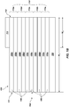
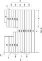
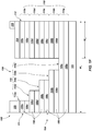
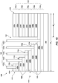
- FIGS. 1A through 1G are simplified partial cross-sectional views illustrating embodiments of a method of forming a semiconductor device structure including a stair step structure, such as a semiconductor device structure for a vertical memory device (e.g., a 3D NAND Flash memory device).
- a stair step structure such as a semiconductor device structure for a vertical memory device (e.g., a 3D NAND Flash memory device).
- a vertical memory device e.g., a 3D NAND Flash memory device.
- a semiconductor device structure 100 may include a substrate 102, and a stack structure 104 exhibiting an alternating sequence of sacrificial structures 106 and insulating structures 108 arranged in tiers 110.
- FIG. 1A shows the stack structure 104 as including five (5) tiers 110 of the sacrificial structures 106 and the insulating structures 108.
- a first tier 110a includes a first sacrificial structure 106a and a first insulating structure 108a over the first sacrificial structure 106a; a second tier 110b overlies the first tier 110a, and includes a second sacrificial structure 106b and a second insulating structure 108b over the second sacrificial structure 106b; a third tier 110c overlies the second tier 110b, and includes a third sacrificial structure 106c and a third insulating structure 108c over the third sacrificial structure 106c; a fourth tier 110d overlies the third tier 110c, and includes a fourth sacrificial structure 106d and a fourth insulating structure 108d over the fourth sacrificial structure 106d; and a fifth tier 110e overlies the fourth tier 110d, and includes a fifth sacrificial structure 106e and a fifth insulating structure 108e over the fifth sacri
- the semiconductor device structure 100 may include a different number of tiers 110.
- the semiconductor device structure 100 may include greater than five (5) tiers 110 (e.g., greater than or equal to ten (10) tiers 110, greater than or equal to twenty-five (25) tiers 110, greater than or equal to fifty (50) tiers 110, greater than or equal to one hundred (100) tiers 110) of the sacrificial structures 106 and the insulating structures 108, or may include less than five (5) tiers 110 (e.g., less than or equal to three (3) tiers 110) of the sacrificial structures 106 and the insulating structures 108.
- the sacrificial structures 106 may each be formed of and include at least one material that may be selectively removed relative to insulating material of the insulating structures 108.
- the at least one material of the sacrificial structures 106 may, for example, comprise one or more of an insulating material (e.g., an insulating material different than the insulating material of the insulating structures 108), a semiconductive material, and a conductive material formulated to be selectively removed relative to the insulating material of the insulating structures 108.
- the sacrificial structures 106 comprise at least one insulating material, such as one or more of an oxide material (e.g., silicon dioxide, phosphosilicate glass, borosilicate glass, borophosphosilicate glass, fluorosilicate glass, titanium dioxide, zirconium dioxide, hafnium dioxide, tantalum oxide, magnesium oxide, aluminum oxide, or combinations thereof), a nitride material (e.g., silicon nitride), an oxynitride material (e.g., silicon oxynitride), amphorous carbon.
- the sacrificial structures 106 comprise at least one semiconductive material, such as undoped polycrystalline silicon.
- the sacrificial structures 106 comprise at least one conductive material, such as conductively-doped polycrystalline silicon.
- Each of the sacrificial structures 106 may independently be substantially homogeneous or substantially heterogeneous. In some embodiments, each of the sacrificial structures 106 is substantially homogeneous. In further embodiments, at least one of the sacrificial structures 106 is substantially heterogeneous.
- One or more of the sacrificial structures 106 may, for example, be formed of and include a stack (e.g., laminate) of at least two different materials. In some embodiments, each of the sacrificial structures 106 is formed of and includes silicon nitride. The sacrificial structures 106 may each be substantially planar, and may each independently exhibit any desired thickness.
- Each of the sacrificial structures 106 may be substantially the same (e.g., exhibit substantially the same material composition, material distribution, size, and shape) as one another, or at least one of the sacrificial structures 106 may be different (e.g., exhibit one or more of a different material composition, a different material distribution, a different size, and a different shape) than at least one other of the sacrificial structures 106.
- each of the first sacrificial structure 106a, the second sacrificial structure 106b, the third sacrificial structure 106c, the fourth sacrificial structure 106d, and the fifth sacrificial structure 106e may exhibit substantially the same material composition, material distribution, and thickness.
- At least one of the first sacrificial structure 106a, the second sacrificial structure 106b, the third sacrificial structure 106c, the fourth sacrificial structure 106d, and the fifth sacrificial structure 106e may exhibit one or more of a different material composition, a different material distribution, and a different thickness than at least one other of the first sacrificial structure 106a, the second sacrificial structure 106b, the third sacrificial structure 106c, the fourth sacrificial structure 106d, and the fifth sacrificial structure 106e.
- each of the sacrificial structures 106 is substantially the same as each other of the sacrificial structures 106.
- the insulating structures 108 may be formed of and include at least one insulating material, such as one or more of an oxide material (e.g., silicon dioxide, phosphosilicate glass, borosilicate glass, borophosphosilicate glass, fluorosilicate glass, titanium dioxide, zirconium dioxide, hafnium dioxide, tantalum oxide, magnesium oxide, aluminum oxide, or a combination thereof), a nitride material (e.g., silicon nitride), an oxynitride material (e.g., silicon oxynitride), and amphorous carbon.
- an oxide material e.g., silicon dioxide, phosphosilicate glass, borosilicate glass, borophosphosilicate glass, fluorosilicate glass, titanium dioxide, zirconium dioxide, hafnium dioxide, tantalum oxide, magnesium oxide, aluminum oxide, or a combination thereof
- a nitride material e.g., silicon nitride
- each of the insulating structures 108 is substantially homogeneous. In additional embodiments, at least one of the insulating structures 108 is substantially heterogeneous.
- One or more of the insulating structures 108 may, for example, be formed of and include a stack (e.g., laminate) of at least two different insulating materials.
- each of the insulating structures 108 is formed of and includes silicon dioxide.
- the insulating structures 108 may each be substantially planar, and may each independently exhibit any desired thickness.
- Each of the insulating structures 108 may be substantially the same (e.g., exhibit substantially the same material composition, material distribution, size, and shape) as one another, or at least one of the insulating structures 108 may be different (e.g., exhibit one or more of a different material composition, a different material distribution, a different size, and a different shape) than at least one other of the insulating structures 108.
- each of the first insulating structure 108a, the second insulating structure 108b, the third insulating structure 108c, the fourth insulating structure 108d, and the fifth insulating structure 108e may exhibit substantially the same material composition, material distribution, and thickness.
- At least one of the first insulating structure 108a, the second insulating structure 108b, the third insulating structure 108c, the fourth insulating structure 108d, and the fifth insulating structure 108e may exhibit one or more of a different material composition, a different material distribution, and a different thickness than at least one other of the first insulating structure 108a, the second insulating structure 108b, the third insulating structure 108c, the fourth insulating structure 108d, and the fifth insulating structure 108e.
- each of the insulating structures 108 is substantially the same as each other of the insulating structures 108.
- the alternating sequence of the sacrificial structures 106 and the insulating structures 108 begins with one of the sacrificial structures 106.
- the sacrificial structures 106 and the insulating structures 108 exhibit a different arrangement relative to one another.
- the sacrificial structures 106 and the insulating structures 108 may be arranged in an alternating sequence beginning with one of the insulating structures 108.
- each of the tiers 110 includes one of the insulating structures 108 on or over one of the sacrificial structures 106.
- each of the tiers 110 includes one of the sacrificial structures 106 on or over one of the insulating structures 108.
- the stack structure 104 may exhibit an elongate shape (e.g., a rectangular shape) extending between a first end 111 and a second, opposing end 112.
- the first end 111 and the second, opposing end 112 of the stack structure 104 may each be, or may each later become, coupled to other components of a semiconductor device (e.g., a memory device) including the semiconductor device structure 100, such as one or more memory cell arrays (e.g., vertical memory cell arrays).
- the stack structure 104 including each of the tiers 110 thereof, may be formed using conventional processes (e.g., conventional deposition processes, conventional material removal processes) and conventional processing equipment, which are not described in detail herein.
- the sacrificial structures 106 and the insulating structures 108 may be formed through one or more of in situ growth, spin-on coating, blanket coating, chemical vapor deposition (CVD), plasma enhanced chemical vapor deposition (PECVD), atomic layer deposition (ALD), and physical vapor deposition (PVD).
- CVD chemical vapor deposition
- PECVD plasma enhanced chemical vapor deposition
- ALD atomic layer deposition
- PVD physical vapor deposition
- a masking structure 114 (e.g., a hard mask structure) may be formed on or over a portion of the stack structure 104.
- the masking structure 114 may be formed of and include at least one material (e.g., at least one hard mask material) suitable for use as an etch mask to pattern portions of the stack structure 104 (e.g., portions of the tiers 110, including portions of the sacrificial structures 106 and portions of the insulating structures 108, remaining uncovered by the masking structure 114) to form at least one staircase structure, as described in further detail below.
- the stack structure 104 may be selectively etchable relative to the masking structure 114.
- a material is "selectively etchable" relative to another material if the material exhibits an etch rate that is at least about five times (5x) greater than the etch rate of another material, such as about ten times (10x) greater, about twenty times (20x) greater, or about forty times (40x) greater.
- the masking structure 114 may be formed of and include one or more of metal-doped carbon, polysilicon, tungsten, and aluminum.
- the masking structure 114 may be formed of and include at one or more of metal-doped carbon, silicon nitride, tungsten, and aluminum. If the masking structure 114 is formed of and includes metal-doped carbon, the metal may, for example, comprise one or more of boron, tungsten, and nickel, and may constitute from about 1.0 weight percent (wt%) to about 30.0 wt% of the metal-doped carbon.
- the masking structure 114 may be homogeneous (e.g., may comprise a single material layer), or may be heterogeneous (e.g., may comprise a stack exhibiting at least two different material layers).
- the dimensions and position of the masking structure 114 may be selected at least partially based on desired positions and desired dimensions of one or more staircase structures to be subsequently formed in the stack structure 104.
- the masking structure 114 may have a width W 2 less than the width W 1 of the stack structure 104, and may be non-centrally positioned over the stack structure 104. Widths of portions of the stack structure 104 remaining uncovered by (e.g., not underlying) the masking structure 114 may correspond to (e.g., be the same as) widths of the one or more staircase structures to be subsequently formed in the stack structure 104.
- the masking structure 114 may exhibit one or more of a different width W 2 , and a different position over the substrate 102.
- the masking structure 114 may have a width W 2 less than the width W 1 of the stack structure 104, and may be centrally positioned on or over the stack structure 104.
- the masking structure 114 may be formed on or over the stack structure 104 to any desired thickness.
- the masking structure 114 exhibits a thickness within a range of from about 10 nanometers (nm) to about 500 nm (e.g., from about 10 nm to about 300 nm, or from about 10 nm to about 100 nm).
- the masking structure 114 may be formed using conventional processes (e.g., conventional deposition processes, such as at least one of in situ growth, spin-on coating, blanket coating, CVD, PECVD, ALD, and PVD; conventional photolithography processes; conventional material removal processes) and conventional processing equipment, which are not described in detail herein.
- conventional deposition processes such as at least one of in situ growth, spin-on coating, blanket coating, CVD, PECVD, ALD, and PVD; conventional photolithography processes; conventional material removal processes
- conventional processing equipment which are not described in detail herein.
- a photoresist 116 may be formed on or over the exposed (e.g., uncovered) portions of the stack structure 104 and the masking structure 114.
- the photoresist 116 may be formed on portions of at least one upper surface of the stack structure 104 (e.g., on portions of an upper surface of the fifth insulating structure 108e) remaining uncovered by the masking structure 114, and on surfaces (e.g., at least one upper surface, at least one side surface) of the masking structure 114.
- the photoresist 116 may function as a mask to remove (e.g., etch) portions of the tiers 110 of the sacrificial structures 106 and the insulating structures 108 and form a stair step structure, as described in further detail below.
- the photoresist 116 may be formed of and include conventional photoresist material, such as a conventional positive tone photoresist material, or a conventional negative tone photoresist material. Suitable photoresist materials are known in the art, and are, therefore, not described in detail herein.
- the photoresist 116 may be compatible with 13.7 nm, 157 nm, 193 nm, 248 nm, or 365 nm wavelength systems; with 193 nm wavelength immersion systems; and/or with electron beam lithographic systems.
- the photoresist 116 may be formed to be non-conformal with the topography of the stack structure 104 and the masking structure 114.
- the photoresist 116 may be formed to exhibit a substantially planar upper surface that does not conform to (e.g., is not the same as) a non-planar topography of an interface between the photoresist 116 and portions of the stack structure 104 and the masking structure 114 adjacent thereto (e.g., directly thereunder).
- an upper boundary (e.g., upper surface) of the photoresist 116 may be substantially planar
- a lower boundary (e.g., lower surface) of the photoresist 116 may be at least partially non-planar.
- the at least partially non-planar topography of the lower boundary may complement the non-planar topography of portions of the stack structure 104 and the masking structure 114 adjacent the lower boundary. Accordingly, the photoresist 116 may exhibit variable (e.g., non-uniform, non-constant) thickness across the width (e.g., the width W 1 ) thereof. For example, as shown in FIG. 1C , portions of the photoresist 116 formed on or over portions of the stack structure 104 uncovered by the masking structure 114 may be thicker than other portions of the photoresist 116 formed on or over the masking structure 114.
- the photoresist 116 may be formed using conventional processes (e.g., conventional deposition processes, such as at least one of in situ growth, spin-on coating, blanket coating, CVD, PECVD, ALD, and PVD; conventional material removal processes) and conventional processing equipment, which are not described in detail herein.
- conventional deposition processes such as at least one of in situ growth, spin-on coating, blanket coating, CVD, PECVD, ALD, and PVD; conventional material removal processes
- conventional processing equipment which are not described in detail herein.
- the semiconductor device structure 100 may be subjected to a first material removal process to remove a first portion of the photoresist 116, and to remove (e.g., etch) a portion of the fifth tier 110e (e.g., including a portion of each of the fifth insulating structure 108e and the fifth sacrificial structure 106e) to a first width using the masking structure 114 and a remaining portion of the photoresist 116 (e.g., a remaining portion of the photoresist 116 not overlying the masking structure 114) as removal (e.g., etching) masks.
- a first material removal process to remove a first portion of the photoresist 116, and to remove (e.g., etch) a portion of the fifth tier 110e (e.g., including a portion of each of the fifth insulating structure 108e and the fifth sacrificial structure 106e) to a first width using the masking structure 114 and a remaining portion
- the first width may correspond to a width of a first step (e.g., a longitudinally lowest step, a step most longitudinally proximate the substrate 102) to be formed through subsequent processing (e.g., subsequent material removal processes), as described in further detail below.
- the first step may, for example, comprise portions of the first sacrificial structure 106a and the first insulating structure 108a not covered by at least one other of the tiers 110 of the sacrificial structures 106 and the insulating structures 108.
- the first material removal process may be controlled so that the portion of the photoresist 116 overlying the masking structure 114 is substantially maintained (e.g., is not substantially removed by the first material removal process). Accordingly, a width of the first portion of the photoresist 116 removed by the first material removal process may be substantially the same as the first width of the fifth tier 110e removed by the first material removal process. In additional embodiments, some of the photoresist 116 overlying the masking structure 114 is removed by the first material removal process.
- a width of the first portion of the photoresist 116 removed by the first material removal process may be different than (e.g., greater than) the first width of the fifth tier 110e removed by the first material removal process.
- the first material removal process may include photolithographically processing the photoresist 116 to remove the first portion of the photoresist 116, and then removing a portion of the fifth tier 110e (e.g., including a portion of each of the fifth insulating structure 108e and the fifth sacrificial structure 106e) not covered by one or more of the masking structure 114 and remaining portions of the photoresist 116 using at least one etching process.
- a portion of the fifth tier 110e e.g., including a portion of each of the fifth insulating structure 108e and the fifth sacrificial structure 106e
- the photoresist 116 may be exposed to an appropriate wavelength (e.g., 13.7 nm, 157 nm, 193 nm, 248 nm, 365 nm) of radiation through a reticle and then developed to remove the first portion of the photoresist 116 and expose a portion of the fifth insulating structure 108e, the exposed portion of the fifth insulating structure 108e may be selectively removed using an etching process (e.g., an anisotropic etching process, such as a dry etching process) to expose a portion of the fifth sacrificial structure 106e, and then the exposed portion of the fifth sacrificial structure 106e may be selectively removed using another etching process (e.g., another anisotropic etching process, such as another dry etching process) to expose a portion of the fourth insulating structure 108d.
- an etching process e.g., an anisotropic etching process, such as a
- Process parameters e.g., radiation wavelengths, developers, etchants, exposure times
- Process parameters may be tailored to the configurations (e.g., material compositions, material distributions, thicknesses, arrangements) of the masking structure 114, the photoresist 116, the insulating structures 108, and the sacrificial structures 106, and are not described in detail herein.
- the semiconductor device structure 100 may be subjected to a second material removal process to remove (e.g., trim) a second portion of the photoresist 116, and to remove (e.g., etch) additional portions of the tiers 110 of the stack structure 104.
- the second material removal process may remove another portion of the fifth tier 110e (e.g., including another portion of each of the fifth insulating structure 108e and the fifth sacrificial structure 106e) to a second width, and may also remove a portion of the fourth tier 110d (e.g., including a portion of each of the fourth insulating structure 108d and the fourth sacrificial structure 106d) to the first width.
- the aforementioned removal of the additional portions of the tiers 110 may employ the masking structure 114 and a newly remaining portion of the photoresist 116 (e.g., a newly remaining portion of the photoresist 116 not overlying the masking structure 114) as removal (e.g., etching) masks.
- the second width may correspond to a width of a second step (e.g., a step longitudinally overlying and adjacent a first step) to be formed through subsequent processing (e.g., subsequent material removal processes), as described in further detail below.
- the second step may, for example, comprise portions of the second sacrificial structure 106b and the second insulating structure 108b not covered by at least one other of the tiers 110 of the sacrificial structures 106 and the insulating structures 108.
- the magnitude of the second width of the fifth tier 110e removed by the second material removal process may be substantially the same as, or may be different than the first width of the fifth tier 110e removed by the first material removal process. In some embodiments, the magnitude of the second width of the fifth tier 110e removed by the second material removal process may be substantially the same as the first width of the fifth tier 110e removed by the first material removal process. In additional embodiments, the magnitude of the second width of the fifth tier 110e removed by the second material removal process is greater than the first width of the fifth tier 110e removed by the first material removal process. In further embodiments, the magnitude of the second width of the fifth tier 110e removed by the second material removal process is less than the first width of the fifth tier 110e removed by the first material removal process.
- the second material removal process may include photolithographically processing the photoresist 116 to remove the second portion of the photoresist 116, and then removing portions of the fifth tier 110e (e.g., including a portion of each of the fifth insulating structure 108e and the fifth sacrificial structure 106e) and the fourth tier 110d (e.g., including a portion of each of the fifth insulating structure 108e and the fifth sacrificial structure 106e) not covered by one or more of the masking structure 114 and newly remaining portions of the photoresist 116 using at least one etching process.
- portions of the fifth tier 110e e.g., including a portion of each of the fifth insulating structure 108e and the fifth sacrificial structure 106e
- the fourth tier 110d e.g., including a portion of each of the fifth insulating structure 108e and the fifth sacrificial structure 106e
- the photoresist 116 may be exposed to an appropriate wavelength (e.g., 13.7 nm, 157 nm, 193 nm, 248 nm, 365 nm) of radiation through a reticle and then developed to trim the second portion from the photoresist 116 and expose an additional portion of the fifth insulating structure 108e, the additional exposed portion of the fifth insulating structure 108e and an exposed portion of the fourth insulating structure 108d may be selectively removed using an etching process (e.g., an anisotropic etching process, such as a dry etching process) to expose an additional portion of the fifth sacrificial structure 106e and a portion of the fourth sacrificial structure 106d, and then the additional exposed portion of the fifth sacrificial structure 106e and the exposed portion of the fourth sacrificial structure 106d may be selectively removed using another etching process (e.g., another anisotropic etching process, such as
- Process parameters (e.g., radiation wavelengths, developers, etchants, exposure times) of the second material removal process may be tailored to the configurations (e.g., material compositions, material distributions, thicknesses, arrangements) of the masking structure 114, the photoresist 116, the insulating structures 108, and the sacrificial structures 106, and are not described in detail herein.
- a duration and an end-point scheme of the second material removal process is substantially the same as a duration and an end-point scheme of the first material removal process.
- one or more of the duration and the end-point scheme of the second material removal process is different than one or more of the duration and the end-point scheme of the first material removal process.
- the semiconductor device structure 100 may be subjected to additional material removal processes to remove (e.g., trim) additional portions of the photoresist 116, the sacrificial structures 106, and the insulating structures 108 and form a stair step structure 120 including steps 118 defined by portions (e.g., ends, exposed surfaces) of the tiers 110.
- additional material removal processes to remove (e.g., trim) additional portions of the photoresist 116, the sacrificial structures 106, and the insulating structures 108 and form a stair step structure 120 including steps 118 defined by portions (e.g., ends, exposed surfaces) of the tiers 110.
- the additional material removal processes may form a first step 118a defined by an exposed surface of the first tier 110a, a second step 118b defined by a lateral end of the second tier 110b, a third step 118c defined by a lateral end of the third tier 110c, a fourth step 118d defined by a lateral of the fourth tier 110d, and a fifth step 118e defined by a lateral end of the fifth tier 110e.
- the additional material removal processes may remove (e.g., trim) additional portions of the photoresist 116 corresponding to widths of the steps 118.
- a third material removal process may remove a third width of the photoresist 116 corresponding to a width of the third step 118c
- a fourth material removal process may remove a fourth width of the photoresist 116 corresponding to a width of the fourth step 118d.
- the width of the fifth step 118e of the stair step structure 120 may correspond to at least a portion of the fifth tier 110e remaining following the additional material removal processes.
- the number of steps 118 included in each of the stair step structure 120 may be substantially the same as (e.g., equal to) or may be different than (e.g., less than, or greater than) the number of tiers 110 in the stack structure 104. In some embodiments, the number of steps 118 included in the stair step structure 120 is the same as the number of tiers 110 in the stack structure 104. As a non-limiting example, as shown in FIG. IF, the stair step structure 120 may include five (5) steps 118 at least partially defined by portions (e.g., exposed upper surfaces, exposed side surfaces) of the five (5) tiers 110 (e.g., tiers 110a through 110e) of the stack structure 104.
- the stair step structure 120 may include a different number of steps 118 (e.g., less than five (5) steps 118, greater than five (5) steps 118).
- the number of steps 118 included in the stair step structure 120 is less than the number of tiers 110 in the stack structure 104.
- the stair step structure 120 may include less than five (5) steps 118 (e.g., four (4) steps 118, three (3) steps 118, two (2) steps 118, etc.) at least partially defined by portions (e.g., exposed upper surfaces, exposed side surfaces) of less than all of the five (5) tiers 110 of the stack structure 104.
- each additional width of the photoresist 116 removed by each of the additional material removal process may be substantially the same, or at least one additional width removed by at least one of the additional material removal processes may be different than at least one other additional width removed by at least one of the additional material removal processes.
- the magnitudes of the additional widths of the tiers 110 removed by the additional material removal process are substantially the same as one another.
- the magnitudes of the additional widths of the tiers 110 removed by the additional material removal process may each be substantially the same as the first width of the fifth tier 110e removed by the first material removal process and/or the second width of the fifth tier 110e removed by the second material removal process.
- the magnitude of at least one additional width of the tiers 110 removed by at least one of the additional material removal processes is greater than the magnitude of at least one other additional width of the tiers 110 removed by at least one other of the additional material removal processes. In further embodiments, the magnitude of at least one additional width of the tiers 110 removed by at least one of the additional material removal processes is less than the magnitude of at least one other additional width of the tiers 110 removed by at least one other of the additional material removal processes.
- the additional material removal processes may each include photolithographically processing the photoresist 116 to remove an additional width of the photoresist 116, and then removing portions of the tiers 110 not covered by one or more of the masking structure 114 and newly remaining portions of the photoresist 116 using at least one etching process.
- Process parameters e.g., radiation wavelengths, developers, etchants, exposure times
- Process parameters of the additional material removal processes may be tailored to the configurations (e.g., material compositions, material distributions, thicknesses, arrangements) of the masking structure 114, the photoresist 116, the insulating structures 108, and the sacrificial structures 106, and are not described in detail herein.
- a duration and an end-point scheme of the one or more of the additional material removal processes is substantially the same as a duration and an end-point scheme of each of the first material removal process, the second material removal process, and each other of the additional material removal processes.
- one or more of a duration and an end-point scheme of the one or more of the additional material removal processes is different than one or more of a duration and an end-point scheme of one or more of the first material removal process, the second material removal process, and at least one other of the additional material removal processes.
- a method of forming a semiconductor device structure comprises forming a stack structure over a substrate, the stack structure comprising tiers each independently comprising a sacrificial structure and an insulating structure longitudinally adjacent the sacrificial structure.
- a masking structure is formed over a portion of the stack structure.
- a photoresist is formed over the masking structure and over additional portions of the stack structure not covered by the masking structure.
- the photoresist and the stack structure are subjected to a series of material removal processes to selectively remove portions of the photoresist and portions of the stack structure not covered by one or more of the masking structure and remaining portions of the photoresist to form a stair step structure.
- the semiconductor device structure 100 may be subjected to additional processing.
- remaining portions of the masking structure 114 (FIG. IF) and the photoresist 116 (FIG. IF) may be removed, at least some portions of the sacrificial structures 106 (FIG. IF) of the tiers 110 may be removed and replaced with conductive structures 122 (e.g., conductive gates, conductive plates) to form a conductive stack structure 126, and conductive contact structures 124 may be formed to provide electrical contact to the conductive structures 122 of the conductive stack structure 126.
- conductive structures 122 e.g., conductive gates, conductive plates
- the remaining portions of the masking structure 114 (FIG. IF) and the photoresist 116 (FIG. IF) may each independently be removed using one or more conventional material removal processes, which are not described in detail herein.
- the remaining portions of the masking structure 114 and the photoresist 116 may each independently be selectively removed through at least one conventional etching process (e.g., a conventional wet etching process, a conventional dry etching process).
- the remaining portions of the masking structure 114 and the photoresist 116 may be removed simultaneously, sequentially, or a combination thereof.
- remaining portions of the photoresist 116 may be removed using a first material removal process, and then remaining portions of the masking structure 114 may be removed using a second material removal process.
- remaining portions of each of the masking structure 114 and the photoresist 116 may be removed substantially simultaneously using one or more material removal processes.
- the conductive structures 122 of the conductive stack structure 126 may be formed of and include at least one conductive material, such as a metal, a metal alloy, a conductive metal oxide, a conductive metal nitride, a conductive metal silicide, a conductively-doped semiconductor material, or combinations thereof.
- the conductive structures 122 may be formed of and include one or more of tungsten, tungsten nitride, nickel, tantalum, tantalum nitride, tantalum silicide, platinum, copper, silver, gold, aluminum, molybdenum, titanium, titanium nitride, titanium silicide, titanium silicon nitride, titanium aluminum nitride, molybdenum nitride, iridium, iridium oxide, ruthenium, ruthenium oxide, and conductively doped silicon.
- the conductive structures 122 are formed of and include tungsten.
- the number of conductive structures 122 included in the conductive stack structure 126 may be substantially the same as (e.g., equal to) or may be different than (e.g., less than, or greater than) the number of tiers 110 in the conductive stack structure 126. In some embodiments, the number of conductive structures 122 included in the conductive stack structure 124 is the same as the number of tiers 110 in the conductive stack structure 126. As a non-limiting example, as shown in FIG.
- the conductive stack structure 126 may include five (5) conductive structures 122 (e.g., a first conductive structure 122a, a second conductive structure 122b, a third conductive structure 122c, a fourth conductive structure 122d, and a fifth conductive structure 122e) formed by removing and replacing portions of the five (5) sacrificial structures 106 (FIG. IF) (e.g., the first sacrificial structure 106a, the second sacrificial structure 106b, the third sacrificial structure 106c, the fourth sacrificial structure 106d, and the fifth sacrificial structure 106e) of the stack structure 104 (FIG. IF).
- five (5) conductive structures 122 e.g., a first conductive structure 122a, a second conductive structure 122b, a third conductive structure 122c, a fourth conductive structure 122d, and a fifth conductive structure 122e
- the conductive stack structure 126 may include a different number of conductive structures 122 (e.g., less than five (5) conductive structures 122, greater than five (5) conductive structures 122).
- the number of conductive structures 122 included in the conductive stack structure 126 is less than the number of tiers 110 in the conductive stack structure 126.
- the conductive structures 122 may be formed by selectively removing portions of the sacrificial structures 106 (FIG. IF) relative to the insulating structures 108 (FIG. IF) to form recessed regions laterally extending into each of the tiers 110, and then at least partially (e.g., substantially) filling the recessed regions with at least one conductive material.
- the recessed regions may be formed by subjecting the stack structure 104 to at least one etching processing (e.g., an isotropic etching process) employing an etch chemistry in which the material (e.g., insulating material, semiconductive material) of the sacrificial structures 108 is selectively removed relative to that of the insulating structures 108.
- the stack structure 104 may be exposed to an etchant comprising phosphoric acid to selectively remove portions of the insulating structures 108 adjacent exposed lateral surfaces of the stack structure 104. Thereafter, the conductive material may be formed (e.g., delivered, deposited) within recessed regions to form the conductive structures 122.
- portions of the insulating structures 108 may instead be selectively removed and replaced with conductive material to form a conductive stack structure.
- a conductive stack structure may be substantially similar to and may have little or no difference in terms of functionality and/or operability as compared to the conductive stack structure 126 depicted in FIG. 1G .
- a method of forming a semiconductor device structure comprises forming a non-conductive stack structure comprising non-conductive tiers over a substrate, each of the non-conductive tiers independently comprising at least two structures longitudinally adjacent one another and having different material compositions than one another.
- a masking structure is formed over a portion of an upper surface of the non-conductive stack structure, the masking structure having a different material composition than the at least two structures of each of the non-conductive tiers of the non-conductive stack structure.
- a non-conformal photoresist is formed over exposed surfaces of the masking structure and the non-conductive stack structure.
- the non-conductive stack structure is subjected to multiple material removal processes using the masking structure and portions of the photoresist as masks to form a stair step structure in the non-conductive stack structure, the stair step structure positioned laterally adjacent the masking structure. At least a portion of one of the least two structures of each of the non-conductive tiers is replaced with a conductive material to form a conductive stack structure comprising partially conductive tiers over the substrate.
- the conductive contact structures 124 may be formed to provide electrical contact to one or more (e.g., each) of the conductive structures 122 (e.g., the first conductive structure 122a of the first tier 110a, the second conductive structure 122b of the second tier 110b, the third conductive structure 122c of the third tier 110c, the fourth conductive structure 122d of the fourth tier 110d, and the fifth conductive structure 122e of the fifth tier 110e) of the conductive stack structure 126.
- the conductive contact structures 124 may, for example, be formed on or over portions of the conductive structures 122 partially defining the steps 118 of the stair step structure 120. For example, as shown in FIG.
- a first conductive contact structure 124a may be formed on or over a portion of the first conductive structure 122a partially defining the first step 118a
- a second conductive contact structure 124b may be formed on or over a portion of the second conductive structure 122b partially defining the second step 118b
- a third conductive contact structure 124c may be formed on or over a portion of the third conductive structure 122c partially defining the third step 118c
- a fourth conductive contact structure 124d may be formed on or over a portion of the fourth conductive structure 122d partially defining the fourth step 118d
- a fifth conductive contact structure 124e may be formed on or over a portion of the fifth conductive structure 122e partially defining the fifth step 118e.
- the conductive contact structures 124 may be formed to exhibit a configuration different than that shown in FIG. 1G .
- the conductive contact structures 124 may be formed to longitudinally extend from each of the conductive structures 122, through the stair step structure 120, and to the substrate 102 (e.g., longitudinally toward the substrate 102 rather than or in addition to longitudinally away from the substrate 102).
- this disclosure is not limited to forming conductive contact structures 124 longitudinally extending from the conductive structures 122 of the semiconductor device structure 100 in a direction longitudinally away from the substrate 102.
- the conductive contact structures 124 may be formed of and include at least one conductive material, such as a metal (e.g., tungsten, titanium, molybdenum, niobium, vanadium, hafnium, tantalum, chromium, zirconium, iron, ruthenium, osmium, cobalt, rhodium, iridium, nickel, palladium, platinum, copper, silver, gold, aluminum), a metal alloy (e.g., a cobalt-based alloy, an iron-based alloy, a nickel-based alloy, an iron- and nickel-based alloy, a cobalt- and nickel-based alloy, an iron- and cobalt-based alloy, a cobalt- and nickel- and iron-based alloy, an aluminum-based alloy, a copper-based alloy, a magnesium-based alloy, a titanium-based alloy, a steel, a low-carbon steel, a stainless steel), a conductive metal-containing material (e.g., a
- the number of conductive contact structures 124 included in the semiconductor device structure 100 may be substantially the same as (e.g., equal to), or may be different than (e.g., less than, or greater than) the number of tiers 110 in the conductive stack structure 126. In some embodiments, the number of conductive contact structures 124 included in the semiconductor device structure 100 is the same as the number of tiers 110 included in the conductive stack structure 126. As a non-limiting example, as shown in FIG. 1G , the semiconductor device structure 100 may include five (5) conductive contact structures 124 each independently coupled to one of the five (5) tiers 110 (e.g., tiers 110a through 110e) of the conductive stack structure 126.
- the semiconductor device structure 100 may include a different number of conductive contact structures 124 (e.g., less than five (5) conductive contact structures 124, greater than five (5) conductive contact structures 124).
- the number of the conductive contact structures 124 included in the semiconductor device structure 100 is less than the number of tiers 110 included in the conductive stack structure 126.
- the number of the conductive contact structures 124 included in the semiconductor device structure 100 is greater than the number of tiers 110 included in the conductive stack structure 126.
- the conductive contact structures 124 may be substantially uniformly (e.g., evenly) spaced apart from one another, or may be non-uniformly (e.g., non-evenly) spaced apart from one another. A magnitude of a distance between adjacent conductive contact structures 124 may at least partially depend on the widths of the steps 118 over which the adjacent conductive contact structures 124 are positioned.
- the conductive contact structures 124 may be formed to be generally centrally positioned on or over each of the steps 118 of the stair step structure 120.
- distances between adjacent conductive contact structures 124 may be substantially the same if the adjacent steps 118 associated with the adjacent conductive contact structures 124 are substantially the same, or vary in accordance with variance (e.g., differences) in the widths of the adjacent steps 118 associated with the adjacent conductive contact structures 124.
- the conductive contact structures 124 may be formed through conventional processes (e.g., conventional material deposition processes, conventional material removal processes), which are not described in detail herein.
- an insulating material e.g., a silicon oxide, silicon nitride, borophosphosilicate glass, a spin-on dielectric
- openings e.g., vias, apertures
- the openings may be filled with a conductive material to form the conductive contact structures 124.
- FIG. 2 illustrates a partial cutaway perspective view of a portion of a semiconductor device 200 (e.g., a vertical memory device, such as a 3D NAND Flash memory device) including a semiconductor device structure 202 including tiers 204 of conductive structures and insulative structures defining a stair step structure 206, and contact structures 208 electrically connected to steps of the stair step structure 206.
- the semiconductor device structure 202 e.g., including the tiers 204 of conductive structures and insulative structures, the stair step structure 206, and the contact structures 208) may be substantially similar to and may be formed in substantially the same manner as the semiconductor device structure 100 previously described in with respect to FIGS. 1A through 1G .
- the semiconductor device 200 may further include vertical strings 212 of memory cells 214 coupled to each other in series, data lines 216 (e.g., bit lines), a source tier 218, access lines 210, first select gates 220 (e.g., upper select gates, drain select gates (SGDs)), select lines 222, a second select gate 224 (e.g., a lower select gate, a source select gate (SGS)), and additional contact structures 226.
- data lines 216 e.g., bit lines
- SGDs drain select gates
- SGS source select gate
- the vertical strings 212 of memory cells 214 extend vertically and orthogonal to conductive lines and tiers (e.g., the data lines 216, the source tier 218, the tiers 204 of the semiconductor device structure 202, the access lines 210, the first select gates 220, the select lines 222, the second select gate 224), and the contact structures 208 and the additional contact structures 226 may electrically couple components to each other as shown (e.g., the select lines 222 to the first select gates 220, the access lines 210 to the tiers 204 of the semiconductor device structure 202).
- conductive lines and tiers e.g., the data lines 216, the source tier 218, the tiers 204 of the semiconductor device structure 202, the access lines 210, the first select gates 220, the select lines 222, the second select gate 224
- the contact structures 208 and the additional contact structures 226 may electrically couple components to each other as shown (e.g., the select lines 222 to the first select gates 220, the
- the semiconductor device 200 may also include a control unit 228 positioned below the memory cells 214, which may include one or more of string driver circuitry, pass gates, circuitry for selecting gates, circuitry for selecting conductive lines (e.g., the data lines 216, the access lines 210), circuitry for amplifying signals, and circuitry for sensing signals.
- the control unit 228 may, for example, be electrically coupled to the data lines 216, source tier 218, access lines 210, first select gates 220, and second select gate 224, for example.
- a semiconductor device comprises a conductive stack structure, a single stair step structure, and conductive contact structures.
- the conductive stack structure comprises tiers each comprising at least one conductive structure and at least one insulating structure longitudinally adjacent the at least one conductive structure.
- the single stair step structure has steps comprising lateral ends of the tiers of the conductive stack structure, and is positioned laterally adjacent a substantially planar lateral surface of the conductive stack structure.
- the conductive contact structures are in physical contact with the steps of the single staircase structure.
- the methods and structures of the disclosure may decrease the lateral dimensions used to form one or more stair step structures for a semiconductor device (e.g., a memory device, such as a 3D NAND Flash memory device) as compared to conventional methods and conventional structures.
- the reduction in the lateral dimensions may permit regions of the semiconductor device to be used for additional purposes (e.g., through vias, interconnect structures, control units) than may otherwise be possible for conventional stair step structure configurations.
- the methods and structures of the disclosure may reduce costs (e.g., manufacturing costs, material costs) and performance, scalability, efficiency, and simplicity as compared to conventional methods and structures.
Landscapes
- Semiconductor Memories (AREA)
- Non-Volatile Memory (AREA)
- Physics & Mathematics (AREA)
- Geometry (AREA)
- Thin Film Transistor (AREA)
- Internal Circuitry In Semiconductor Integrated Circuit Devices (AREA)
- Element Separation (AREA)
Abstract
Description
- This application claims the benefit of the filing date of United States Patent Application Serial No.
15/271,924, filed September 21, 2016 - The disclosure, in various embodiments, relates generally to the field of semiconductor device design and fabrication. More specifically, the disclosure relates to methods of forming a semiconductor device structure including a stair step structure, and to related semiconductor device structures and semiconductor devices.
- A continuing goal of the semiconductor industry has been to increase the memory density (e.g., the number of memory cells per memory die) of memory devices, such as non-volatile memory devices (e.g., NAND Flash memory devices). One way of increasing memory density in non-volatile memory devices is to utilize vertical memory array (also referred to as a "three-dimensional (3D) memory array") architectures. A typical vertical memory array includes semiconductor pillars extending through openings in tiers of conductive structures (e.g., word line plates, control gate plates) and dielectric materials at each junction of the semiconductor pillars and the conductive structures. Such a configuration permits a greater number of transistors to be located in a unit of die area by building the array upwards (e.g., longitudinally, vertically) on a die, as compared to structures with conventional planar (e.g., two-dimensional) arrangements of transistors.
- Conventional vertical memory arrays include electrical connections between the conductive structures and access lines (e.g., word lines) so that memory cells in the vertical memory array can be uniquely selected for writing, reading, or erasing operations. One method of forming such an electrical connection includes forming a so-called "stair step" structure at edges (e.g., lateral ends) of the tiers of conductive structures. The stair step structure includes individual "steps" defining contact regions of the conductive structures upon which contact structures can be positioned to provide electrical access to the conductive structures.
- Conventional processes for forming a stair step structure generally include repeated acts of trimming a photoresist overlying alternating conductive structures and insulating structures, etching portions of the insulating structures not covered by a remaining portion of the photoresist, and then etching portions of the conductive structures not covered by remaining portions of the insulating structures. Such conventional processes typically result in the formation of so-called "stadium" structures exhibiting opposing and symmetric stair step structures. A first stair step structure on a first end of a stadium structure typically mirrors a second stair step structure on a second end of the stadium structure. The first stair step structure and the second stair step structure generally exhibit substantially the same size and substantially the same shape, but the first stair step structure outwardly extends in a direction that opposes a direction in which the second stair step structure outwardly extends. For various applications, however, only one stair step structure (e.g., only the first stair step structure or only the second stair step structure) of the stadium structure is used to make electrical connections, and the other stair step structure (e.g., the second stair step structure or the first stair step structure) of the stadium structure is underutilized and/or occupies space that could otherwise be utilized for another, more desirable purpose.
- It would, therefore, be desirable to have improved methods of forming stair step structures for semiconductor devices (e.g., vertical memory devices, such as 3D NAND Flash memory devices) that reduce, if not eliminate, the aforementioned problems.
-
-
FIGS. 1A through 1G are cross-sectional views illustrating different process stages and structures for a method of forming a semiconductor device structure including a stair step structure, in accordance with an embodiment of the disclosure. -
FIG. 2 is a partial cutaway perspective view of a vertical memory device including a semiconductor device structure having a stair step structure, in accordance with an embodiment of the disclosure. - Methods of forming a semiconductor device structure including a stair step structure are described, as are related semiconductor device structures and semiconductor devices (e.g., vertical memory devices, such as 3D NAND Flash memory devices). In some embodiments, a method of forming a semiconductor device structure includes forming a stack structure over a substrate. The stack structure may include sacrificial structures and insulating structures arranged in tiers. Each of the tiers may independently include one of the sacrificial structures and one of the insulating structures. A masking structure (e.g., a hard mask structure) may be formed on or over a portion of the stack structure, and a photoresist may be formed on or over the masking structure and on or over additional portions of the stack structure not covered by the masking structure. The photoresist and the stack structure may then be subjected to a series of material removal processes to form a stair step structure. The material removal processes may selectively remove portions of the photoresist, and may also selectively remove portions of the stack structure not covered by one or more of the masking structure and remaining portions of the photoresist. The configuration and position of the masking structure facilitates the formation of the stair step structure without the formation of an opposing stair step structure that mirrors (e.g., is the mirror image of) the stair step structure. Following the formation of the stair step structure, remaining portions of the masking structure and the photoresist (if any) may be removed, and at least a portion of the sacrificial structure of each of the tiers may be replaced with at least one conductive material to form a conductive structure in each of the tiers. Conductive contact structures may then be coupled to the conductive structures of the tiers at the steps of the stair step structure. The methods and structures of the disclosure may enhance the utilized space of semiconductor device structures including stair step structures, facilitating the efficient formation of semiconductive devices exhibiting improved performance as compared to conventional semiconductive devices.
- The following description provides specific details, such as material compositions and processing conditions, in order to provide a thorough description of embodiments of the present disclosure. However, a person of ordinary skill in the art would understand that the embodiments of the present disclosure may be practiced without employing these specific details. Indeed, the embodiments of the present disclosure may be practiced in conjunction with conventional semiconductor fabrication techniques employed in the industry. In addition, the description provided below does not form a complete process flow for manufacturing a semiconductor device. The semiconductor device structures described below do not form a complete semiconductor device. Only those process acts and structures necessary to understand the embodiments of the present disclosure are described in detail below. Additional acts to form a complete semiconductor device from the semiconductor device structures may be performed by conventional fabrication techniques.
- Drawings presented herein are for illustrative purposes only, and are not meant to be actual views of any particular material, component, structure, device, or system. Variations from the shapes depicted in the drawings as a result, for example, of manufacturing techniques and/or tolerances, are to be expected. Thus, embodiments described herein are not to be construed as being limited to the particular shapes or regions as illustrated, but include deviations in shapes that result, for example, from manufacturing. For example, a region illustrated or described as box-shaped may have rough and/or nonlinear features, and a region illustrated or described as round may include some rough and/or linear features. Moreover, sharp angles that are illustrated may be rounded, and vice versa. Thus, the regions illustrated in the figures are schematic in nature, and their shapes are not intended to illustrate the precise shape of a region and do not limit the scope of the present claims. The drawings are not necessarily to scale. Additionally, elements common between figures may retain the same numerical designation.
- As used herein, the term "substrate" means and includes a base material or construction upon which additional materials are formed. The substrate may be a semiconductor substrate, a base semiconductor layer on a supporting structure, a metal electrode, or a semiconductor substrate having one or more layers, structures or regions formed thereon. The substrate may be a conventional silicon substrate or other bulk substrate comprising a layer of semiconductive material. As used herein, the term "bulk substrate" means and includes not only silicon wafers, but also silicon-on-insulator (SOI) substrates, such as silicon-on-sapphire (SOS) substrates and silicon-on-glass (SOG) substrates, epitaxial layers of silicon on a base semiconductor foundation, and other semiconductor or optoelectronic materials, such as silicon-germanium, germanium, gallium arsenide, gallium nitride, and indium phosphide. The substrate may be doped or undoped. By way of non-limiting example, a substrate may comprise at least one of silicon, silicon dioxide, silicon with native oxide, silicon nitride, a carbon-containing silicon nitride, glass, semiconductor, metal oxide, metal, a titanium nitride, a carbon-containing titanium nitride, tantalum, a tantalum nitride, a carbon-containing tantalum nitride, niobium, a niobium nitride, a carbon-containing niobium nitride, molybdenum, a molybdenum nitride, a carbon-containing molybdenum nitride, tungsten, a tungsten nitride, a carbon-containing tungsten nitride, copper, cobalt, nickel, iron, aluminum, and a noble metal.
- As used herein, the terms "vertical", "longitudinal", "horizontal", and "lateral" are in reference to a major plane of a substrate in or on which the structures described are formed and are not necessarily defined by earth's gravitational field. A "horizontal" or "lateral" direction is a direction that is substantially parallel to the major plane of the substrate, while a "vertical" or "longitudinal" direction is a direction that is substantially perpendicular to the major plane of the substrate. The major plane of the substrate is defined by a surface of the substrate having a relatively large area compared to other surfaces of the substrate, such as by a substantially planar circular surface of a conventional semiconductor wafer substrate.
- As used herein, spatially relative terms, such as "beneath," "below," "lower," "bottom," "above," "upper," "top," "front," "rear," "left," "right," and the like, may be used for ease of description to describe one element's or feature's relationship to another element(s) or feature(s) as illustrated in the figures. Unless otherwise specified, the spatially relative terms are intended to encompass different orientations of the materials in addition to the orientation depicted in the figures. For example, if materials in the figures are inverted, elements described as "below," or "beneath," or "under," or "on bottom of' other elements or features would then be oriented "above" or "on top of' the other elements or features. Thus, the term "below" can encompass both an orientation of above and below, depending on the context in which the term is used, which will be evident to one of ordinary skill in the art. The materials may be otherwise oriented (e.g., rotated 90 degrees, inverted, flipped) and the spatially relative descriptors used herein interpreted accordingly.
- As used herein, the singular forms "a," "an," and "the" are intended to include the plural forms as well, unless the context clearly indicates otherwise.
- As used herein, "and/or" includes any and all combinations of one or more of the associated listed items.
- As used herein, the term "configured" refers to a size, shape, material composition, and arrangement of one or more of at least one structure and at least one apparatus facilitating operation of one or more of the structure and the apparatus in a pre-determined way.
- As used herein, the term "substantially" in reference to a given parameter, property, or condition means and includes to a degree that one of ordinary skill in the art would understand that the given parameter, property, or condition is met with a degree of variance, such as within acceptable manufacturing tolerances. By way of example, depending on the particular parameter, property, or condition that is substantially met, the parameter, property, or condition may be at least 90.0% met, at least 95.0% met, at least 99.0% met, or even at least 99.9% met.
- As used herein, the term "about" in reference to a given parameter is inclusive of the stated value and has the meaning dictated by the context (e.g., it includes the degree of error associated with measurement of the given parameter).
-
FIGS. 1A through 1G are simplified partial cross-sectional views illustrating embodiments of a method of forming a semiconductor device structure including a stair step structure, such as a semiconductor device structure for a vertical memory device (e.g., a 3D NAND Flash memory device). With the description provided below, it will be readily apparent to one of ordinary skill in the art that the methods described herein may be used in various devices. In other words, the methods of the disclosure may be used whenever it is desired to form a stair step structure. - Referring to
FIG. 1A , asemiconductor device structure 100 may include asubstrate 102, and astack structure 104 exhibiting an alternating sequence ofsacrificial structures 106 and insulatingstructures 108 arranged intiers 110. For clarity and ease of understanding of the drawings and related description,FIG. 1A shows thestack structure 104 as including five (5)tiers 110 of thesacrificial structures 106 and the insulatingstructures 108. Afirst tier 110a includes a firstsacrificial structure 106a and a firstinsulating structure 108a over the firstsacrificial structure 106a; asecond tier 110b overlies thefirst tier 110a, and includes a secondsacrificial structure 106b and a secondinsulating structure 108b over the secondsacrificial structure 106b; athird tier 110c overlies thesecond tier 110b, and includes a thirdsacrificial structure 106c and a thirdinsulating structure 108c over the thirdsacrificial structure 106c; afourth tier 110d overlies thethird tier 110c, and includes a fourthsacrificial structure 106d and a fourthinsulating structure 108d over the fourthsacrificial structure 106d; and afifth tier 110e overlies thefourth tier 110d, and includes a fifthsacrificial structure 106e and a fifthinsulating structure 108e over the fifthsacrificial structure 106e. However, thesemiconductor device structure 100 may include a different number oftiers 110. For example, in additional embodiments, thesemiconductor device structure 100 may include greater than five (5) tiers 110 (e.g., greater than or equal to ten (10)tiers 110, greater than or equal to twenty-five (25)tiers 110, greater than or equal to fifty (50)tiers 110, greater than or equal to one hundred (100) tiers 110) of thesacrificial structures 106 and the insulatingstructures 108, or may include less than five (5) tiers 110 (e.g., less than or equal to three (3) tiers 110) of thesacrificial structures 106 and the insulatingstructures 108. - The
sacrificial structures 106 may each be formed of and include at least one material that may be selectively removed relative to insulating material of the insulatingstructures 108. The at least one material of thesacrificial structures 106 may, for example, comprise one or more of an insulating material (e.g., an insulating material different than the insulating material of the insulating structures 108), a semiconductive material, and a conductive material formulated to be selectively removed relative to the insulating material of the insulatingstructures 108. In some embodiments, thesacrificial structures 106 comprise at least one insulating material, such as one or more of an oxide material (e.g., silicon dioxide, phosphosilicate glass, borosilicate glass, borophosphosilicate glass, fluorosilicate glass, titanium dioxide, zirconium dioxide, hafnium dioxide, tantalum oxide, magnesium oxide, aluminum oxide, or combinations thereof), a nitride material (e.g., silicon nitride), an oxynitride material (e.g., silicon oxynitride), amphorous carbon. In additional embodiments, thesacrificial structures 106 comprise at least one semiconductive material, such as undoped polycrystalline silicon. In further embodiments, thesacrificial structures 106 comprise at least one conductive material, such as conductively-doped polycrystalline silicon. Each of thesacrificial structures 106 may independently be substantially homogeneous or substantially heterogeneous. In some embodiments, each of thesacrificial structures 106 is substantially homogeneous. In further embodiments, at least one of thesacrificial structures 106 is substantially heterogeneous. One or more of thesacrificial structures 106 may, for example, be formed of and include a stack (e.g., laminate) of at least two different materials. In some embodiments, each of thesacrificial structures 106 is formed of and includes silicon nitride. Thesacrificial structures 106 may each be substantially planar, and may each independently exhibit any desired thickness. - Each of the
sacrificial structures 106 may be substantially the same (e.g., exhibit substantially the same material composition, material distribution, size, and shape) as one another, or at least one of thesacrificial structures 106 may be different (e.g., exhibit one or more of a different material composition, a different material distribution, a different size, and a different shape) than at least one other of thesacrificial structures 106. As non-limiting example, each of the firstsacrificial structure 106a, the secondsacrificial structure 106b, the thirdsacrificial structure 106c, the fourthsacrificial structure 106d, and the fifthsacrificial structure 106e may exhibit substantially the same material composition, material distribution, and thickness. As another non-limiting example, at least one of the firstsacrificial structure 106a, the secondsacrificial structure 106b, the thirdsacrificial structure 106c, the fourthsacrificial structure 106d, and the fifthsacrificial structure 106e may exhibit one or more of a different material composition, a different material distribution, and a different thickness than at least one other of the firstsacrificial structure 106a, the secondsacrificial structure 106b, the thirdsacrificial structure 106c, the fourthsacrificial structure 106d, and the fifthsacrificial structure 106e. In some embodiments, each of thesacrificial structures 106 is substantially the same as each other of thesacrificial structures 106. - The insulating
structures 108 may be formed of and include at least one insulating material, such as one or more of an oxide material (e.g., silicon dioxide, phosphosilicate glass, borosilicate glass, borophosphosilicate glass, fluorosilicate glass, titanium dioxide, zirconium dioxide, hafnium dioxide, tantalum oxide, magnesium oxide, aluminum oxide, or a combination thereof), a nitride material (e.g., silicon nitride), an oxynitride material (e.g., silicon oxynitride), and amphorous carbon. Each of the insulatingstructures 108 may independently be substantially homogeneous or substantially heterogeneous. In some embodiments, each of the insulatingstructures 108 is substantially homogeneous. In additional embodiments, at least one of the insulatingstructures 108 is substantially heterogeneous. One or more of the insulatingstructures 108 may, for example, be formed of and include a stack (e.g., laminate) of at least two different insulating materials. In some embodiments, each of the insulatingstructures 108 is formed of and includes silicon dioxide. The insulatingstructures 108 may each be substantially planar, and may each independently exhibit any desired thickness. - Each of the insulating
structures 108 may be substantially the same (e.g., exhibit substantially the same material composition, material distribution, size, and shape) as one another, or at least one of the insulatingstructures 108 may be different (e.g., exhibit one or more of a different material composition, a different material distribution, a different size, and a different shape) than at least one other of the insulatingstructures 108. As non-limiting example, each of the firstinsulating structure 108a, the secondinsulating structure 108b, the thirdinsulating structure 108c, the fourthinsulating structure 108d, and the fifthinsulating structure 108e may exhibit substantially the same material composition, material distribution, and thickness. As another non-limiting example, at least one of the firstinsulating structure 108a, the secondinsulating structure 108b, the thirdinsulating structure 108c, the fourthinsulating structure 108d, and the fifthinsulating structure 108e may exhibit one or more of a different material composition, a different material distribution, and a different thickness than at least one other of the firstinsulating structure 108a, the secondinsulating structure 108b, the thirdinsulating structure 108c, the fourthinsulating structure 108d, and the fifthinsulating structure 108e. In some embodiments, each of the insulatingstructures 108 is substantially the same as each other of the insulatingstructures 108. - As shown in
FIG. 1A , in some embodiments, the alternating sequence of thesacrificial structures 106 and the insulatingstructures 108 begins with one of thesacrificial structures 106. In additional embodiments, thesacrificial structures 106 and the insulatingstructures 108 exhibit a different arrangement relative to one another. By way of non-limiting example, thesacrificial structures 106 and the insulatingstructures 108 may be arranged in an alternating sequence beginning with one of the insulatingstructures 108. In some embodiments, each of thetiers 110 includes one of the insulatingstructures 108 on or over one of thesacrificial structures 106. In additional embodiments, each of thetiers 110 includes one of thesacrificial structures 106 on or over one of the insulatingstructures 108. - The
stack structure 104 may exhibit an elongate shape (e.g., a rectangular shape) extending between afirst end 111 and a second, opposingend 112. Thefirst end 111 and the second, opposingend 112 of thestack structure 104 may each be, or may each later become, coupled to other components of a semiconductor device (e.g., a memory device) including thesemiconductor device structure 100, such as one or more memory cell arrays (e.g., vertical memory cell arrays). - The
stack structure 104, including each of thetiers 110 thereof, may be formed using conventional processes (e.g., conventional deposition processes, conventional material removal processes) and conventional processing equipment, which are not described in detail herein. By way of non-limiting example, thesacrificial structures 106 and the insulatingstructures 108 may be formed through one or more of in situ growth, spin-on coating, blanket coating, chemical vapor deposition (CVD), plasma enhanced chemical vapor deposition (PECVD), atomic layer deposition (ALD), and physical vapor deposition (PVD). - Referring next to
FIG. 1B , a masking structure 114 (e.g., a hard mask structure) may be formed on or over a portion of thestack structure 104. The maskingstructure 114 may be formed of and include at least one material (e.g., at least one hard mask material) suitable for use as an etch mask to pattern portions of the stack structure 104 (e.g., portions of thetiers 110, including portions of thesacrificial structures 106 and portions of the insulatingstructures 108, remaining uncovered by the masking structure 114) to form at least one staircase structure, as described in further detail below. Thestack structure 104 may be selectively etchable relative to the maskingstructure 114. As used herein, a material is "selectively etchable" relative to another material if the material exhibits an etch rate that is at least about five times (5x) greater than the etch rate of another material, such as about ten times (10x) greater, about twenty times (20x) greater, or about forty times (40x) greater. As a non-limiting example, at least in embodiments wherein thesacrificial structures 106 comprise silicon nitride and the insulatingstructures 108 comprise silicon dioxide, or vice versa, the maskingstructure 114 may be formed of and include one or more of metal-doped carbon, polysilicon, tungsten, and aluminum. As another non-limiting example, at least in embodiments wherein thesacrificial structures 106 comprise polycrystalline silicon (e.g., undoped polycrystalline silicon, doped polycrystalline silicon) and the insulatingstructures 108 comprise silicon dioxide, or vice versa, the maskingstructure 114 may be formed of and include at one or more of metal-doped carbon, silicon nitride, tungsten, and aluminum. If the maskingstructure 114 is formed of and includes metal-doped carbon, the metal may, for example, comprise one or more of boron, tungsten, and nickel, and may constitute from about 1.0 weight percent (wt%) to about 30.0 wt% of the metal-doped carbon. The maskingstructure 114 may be homogeneous (e.g., may comprise a single material layer), or may be heterogeneous (e.g., may comprise a stack exhibiting at least two different material layers). - The dimensions and position of the masking
structure 114 may be selected at least partially based on desired positions and desired dimensions of one or more staircase structures to be subsequently formed in thestack structure 104. By way of non-limiting example, as shown inFIG. 1B , the maskingstructure 114 may have a width W2 less than the width W1 of thestack structure 104, and may be non-centrally positioned over thestack structure 104. Widths of portions of thestack structure 104 remaining uncovered by (e.g., not underlying) themasking structure 114 may correspond to (e.g., be the same as) widths of the one or more staircase structures to be subsequently formed in thestack structure 104. In additional embodiments, the maskingstructure 114 may exhibit one or more of a different width W2, and a different position over thesubstrate 102. As a non-limiting example, the maskingstructure 114 may have a width W2 less than the width W1 of thestack structure 104, and may be centrally positioned on or over thestack structure 104. The maskingstructure 114 may be formed on or over thestack structure 104 to any desired thickness. In some embodiments, the maskingstructure 114 exhibits a thickness within a range of from about 10 nanometers (nm) to about 500 nm (e.g., from about 10 nm to about 300 nm, or from about 10 nm to about 100 nm). - The masking
structure 114 may be formed using conventional processes (e.g., conventional deposition processes, such as at least one of in situ growth, spin-on coating, blanket coating, CVD, PECVD, ALD, and PVD; conventional photolithography processes; conventional material removal processes) and conventional processing equipment, which are not described in detail herein. - Referring next to
FIG. 1C , aphotoresist 116 may be formed on or over the exposed (e.g., uncovered) portions of thestack structure 104 and the maskingstructure 114. For example, as shown inFIG. 1C , thephotoresist 116 may be formed on portions of at least one upper surface of the stack structure 104 (e.g., on portions of an upper surface of the fifthinsulating structure 108e) remaining uncovered by the maskingstructure 114, and on surfaces (e.g., at least one upper surface, at least one side surface) of the maskingstructure 114. Thephotoresist 116 may function as a mask to remove (e.g., etch) portions of thetiers 110 of thesacrificial structures 106 and the insulatingstructures 108 and form a stair step structure, as described in further detail below. Thephotoresist 116 may be formed of and include conventional photoresist material, such as a conventional positive tone photoresist material, or a conventional negative tone photoresist material. Suitable photoresist materials are known in the art, and are, therefore, not described in detail herein. Thephotoresist 116 may be compatible with 13.7 nm, 157 nm, 193 nm, 248 nm, or 365 nm wavelength systems; with 193 nm wavelength immersion systems; and/or with electron beam lithographic systems. - The
photoresist 116 may be formed to be non-conformal with the topography of thestack structure 104 and the maskingstructure 114. For example, as shown inFIG. 1C , thephotoresist 116 may be formed to exhibit a substantially planar upper surface that does not conform to (e.g., is not the same as) a non-planar topography of an interface between thephotoresist 116 and portions of thestack structure 104 and the maskingstructure 114 adjacent thereto (e.g., directly thereunder). Put another way, an upper boundary (e.g., upper surface) of thephotoresist 116 may be substantially planar, and a lower boundary (e.g., lower surface) of thephotoresist 116 may be at least partially non-planar. The at least partially non-planar topography of the lower boundary may complement the non-planar topography of portions of thestack structure 104 and the maskingstructure 114 adjacent the lower boundary. Accordingly, thephotoresist 116 may exhibit variable (e.g., non-uniform, non-constant) thickness across the width (e.g., the width W1) thereof. For example, as shown inFIG. 1C , portions of thephotoresist 116 formed on or over portions of thestack structure 104 uncovered by the maskingstructure 114 may be thicker than other portions of thephotoresist 116 formed on or over the maskingstructure 114. - The
photoresist 116 may be formed using conventional processes (e.g., conventional deposition processes, such as at least one of in situ growth, spin-on coating, blanket coating, CVD, PECVD, ALD, and PVD; conventional material removal processes) and conventional processing equipment, which are not described in detail herein. - Referring next to FIG. ID, the
semiconductor device structure 100 may be subjected to a first material removal process to remove a first portion of thephotoresist 116, and to remove (e.g., etch) a portion of thefifth tier 110e (e.g., including a portion of each of the fifthinsulating structure 108e and the fifthsacrificial structure 106e) to a first width using themasking structure 114 and a remaining portion of the photoresist 116 (e.g., a remaining portion of thephotoresist 116 not overlying the masking structure 114) as removal (e.g., etching) masks. The first width may correspond to a width of a first step (e.g., a longitudinally lowest step, a step most longitudinally proximate the substrate 102) to be formed through subsequent processing (e.g., subsequent material removal processes), as described in further detail below. The first step may, for example, comprise portions of the firstsacrificial structure 106a and the firstinsulating structure 108a not covered by at least one other of thetiers 110 of thesacrificial structures 106 and the insulatingstructures 108. - As shown in FIG. ID, in some embodiments, the first material removal process may be controlled so that the portion of the
photoresist 116 overlying the maskingstructure 114 is substantially maintained (e.g., is not substantially removed by the first material removal process). Accordingly, a width of the first portion of thephotoresist 116 removed by the first material removal process may be substantially the same as the first width of thefifth tier 110e removed by the first material removal process. In additional embodiments, some of thephotoresist 116 overlying the maskingstructure 114 is removed by the first material removal process. For example, some of thephotoresist 116 overlying the maskingstructure 114 and positioned laterally proximate a lateral boundary (e.g., a side surface) of the maskingstructure 114 may be removed in addition to some of thephotoresist 116 not overlying the maskingstructure 114. Accordingly, in such embodiments, a width of the first portion of thephotoresist 116 removed by the first material removal process may be different than (e.g., greater than) the first width of thefifth tier 110e removed by the first material removal process. - The first material removal process may include photolithographically processing the
photoresist 116 to remove the first portion of thephotoresist 116, and then removing a portion of thefifth tier 110e (e.g., including a portion of each of the fifthinsulating structure 108e and the fifthsacrificial structure 106e) not covered by one or more of the maskingstructure 114 and remaining portions of thephotoresist 116 using at least one etching process. For example, thephotoresist 116 may be exposed to an appropriate wavelength (e.g., 13.7 nm, 157 nm, 193 nm, 248 nm, 365 nm) of radiation through a reticle and then developed to remove the first portion of thephotoresist 116 and expose a portion of the fifthinsulating structure 108e, the exposed portion of the fifthinsulating structure 108e may be selectively removed using an etching process (e.g., an anisotropic etching process, such as a dry etching process) to expose a portion of the fifthsacrificial structure 106e, and then the exposed portion of the fifthsacrificial structure 106e may be selectively removed using another etching process (e.g., another anisotropic etching process, such as another dry etching process) to expose a portion of the fourthinsulating structure 108d. Process parameters (e.g., radiation wavelengths, developers, etchants, exposure times) of the first material removal process may be tailored to the configurations (e.g., material compositions, material distributions, thicknesses, arrangements) of the maskingstructure 114, thephotoresist 116, the insulatingstructures 108, and thesacrificial structures 106, and are not described in detail herein. - Referring next to FIG. IE, the
semiconductor device structure 100 may be subjected to a second material removal process to remove (e.g., trim) a second portion of thephotoresist 116, and to remove (e.g., etch) additional portions of thetiers 110 of thestack structure 104. The second material removal process may remove another portion of thefifth tier 110e (e.g., including another portion of each of the fifthinsulating structure 108e and the fifthsacrificial structure 106e) to a second width, and may also remove a portion of thefourth tier 110d (e.g., including a portion of each of the fourthinsulating structure 108d and the fourthsacrificial structure 106d) to the first width. The aforementioned removal of the additional portions of thetiers 110 may employ the maskingstructure 114 and a newly remaining portion of the photoresist 116 (e.g., a newly remaining portion of thephotoresist 116 not overlying the masking structure 114) as removal (e.g., etching) masks. The second width may correspond to a width of a second step (e.g., a step longitudinally overlying and adjacent a first step) to be formed through subsequent processing (e.g., subsequent material removal processes), as described in further detail below. The second step may, for example, comprise portions of the secondsacrificial structure 106b and the secondinsulating structure 108b not covered by at least one other of thetiers 110 of thesacrificial structures 106 and the insulatingstructures 108. - The magnitude of the second width of the
fifth tier 110e removed by the second material removal process may be substantially the same as, or may be different than the first width of thefifth tier 110e removed by the first material removal process. In some embodiments, the magnitude of the second width of thefifth tier 110e removed by the second material removal process may be substantially the same as the first width of thefifth tier 110e removed by the first material removal process. In additional embodiments, the magnitude of the second width of thefifth tier 110e removed by the second material removal process is greater than the first width of thefifth tier 110e removed by the first material removal process. In further embodiments, the magnitude of the second width of thefifth tier 110e removed by the second material removal process is less than the first width of thefifth tier 110e removed by the first material removal process. - The second material removal process may include photolithographically processing the
photoresist 116 to remove the second portion of thephotoresist 116, and then removing portions of thefifth tier 110e (e.g., including a portion of each of the fifthinsulating structure 108e and the fifthsacrificial structure 106e) and thefourth tier 110d (e.g., including a portion of each of the fifthinsulating structure 108e and the fifthsacrificial structure 106e) not covered by one or more of the maskingstructure 114 and newly remaining portions of thephotoresist 116 using at least one etching process. For example, thephotoresist 116 may be exposed to an appropriate wavelength (e.g., 13.7 nm, 157 nm, 193 nm, 248 nm, 365 nm) of radiation through a reticle and then developed to trim the second portion from thephotoresist 116 and expose an additional portion of the fifthinsulating structure 108e, the additional exposed portion of the fifthinsulating structure 108e and an exposed portion of the fourthinsulating structure 108d may be selectively removed using an etching process (e.g., an anisotropic etching process, such as a dry etching process) to expose an additional portion of the fifthsacrificial structure 106e and a portion of the fourthsacrificial structure 106d, and then the additional exposed portion of the fifthsacrificial structure 106e and the exposed portion of the fourthsacrificial structure 106d may be selectively removed using another etching process (e.g., another anisotropic etching process, such as another dry etching process) to expose an additional portion of the fourthinsulating structure 108d and a portion of the thirdinsulating structure 108c. Process parameters (e.g., radiation wavelengths, developers, etchants, exposure times) of the second material removal process may be tailored to the configurations (e.g., material compositions, material distributions, thicknesses, arrangements) of the maskingstructure 114, thephotoresist 116, the insulatingstructures 108, and thesacrificial structures 106, and are not described in detail herein. In some embodiments, a duration and an end-point scheme of the second material removal process is substantially the same as a duration and an end-point scheme of the first material removal process. In additional embodiments, one or more of the duration and the end-point scheme of the second material removal process is different than one or more of the duration and the end-point scheme of the first material removal process. - Referring next to FIG. IF, the
semiconductor device structure 100 may be subjected to additional material removal processes to remove (e.g., trim) additional portions of thephotoresist 116, thesacrificial structures 106, and the insulatingstructures 108 and form astair step structure 120 includingsteps 118 defined by portions (e.g., ends, exposed surfaces) of thetiers 110. For example, as shown in FIG. IF, the additional material removal processes may form afirst step 118a defined by an exposed surface of thefirst tier 110a, asecond step 118b defined by a lateral end of thesecond tier 110b, athird step 118c defined by a lateral end of thethird tier 110c, afourth step 118d defined by a lateral of thefourth tier 110d, and afifth step 118e defined by a lateral end of thefifth tier 110e. The additional material removal processes may remove (e.g., trim) additional portions of thephotoresist 116 corresponding to widths of thesteps 118. For example, a third material removal process may remove a third width of thephotoresist 116 corresponding to a width of thethird step 118c, and a fourth material removal process may remove a fourth width of thephotoresist 116 corresponding to a width of thefourth step 118d. The width of thefifth step 118e of thestair step structure 120 may correspond to at least a portion of thefifth tier 110e remaining following the additional material removal processes. - The number of
steps 118 included in each of thestair step structure 120 may be substantially the same as (e.g., equal to) or may be different than (e.g., less than, or greater than) the number oftiers 110 in thestack structure 104. In some embodiments, the number ofsteps 118 included in thestair step structure 120 is the same as the number oftiers 110 in thestack structure 104. As a non-limiting example, as shown in FIG. IF, thestair step structure 120 may include five (5)steps 118 at least partially defined by portions (e.g., exposed upper surfaces, exposed side surfaces) of the five (5) tiers 110 (e.g.,tiers 110a through 110e) of thestack structure 104. In additional embodiments, thestair step structure 120 may include a different number of steps 118 (e.g., less than five (5) steps 118, greater than five (5) steps 118). For example, in additional embodiments, the number ofsteps 118 included in thestair step structure 120 is less than the number oftiers 110 in thestack structure 104. As a non-limiting example, thestair step structure 120 may include less than five (5) steps 118 (e.g., four (4) steps 118, three (3) steps 118, two (2) steps 118, etc.) at least partially defined by portions (e.g., exposed upper surfaces, exposed side surfaces) of less than all of the five (5)tiers 110 of thestack structure 104. - The magnitude of each additional width of the
photoresist 116 removed by each of the additional material removal process may be substantially the same, or at least one additional width removed by at least one of the additional material removal processes may be different than at least one other additional width removed by at least one of the additional material removal processes. In some embodiments, the magnitudes of the additional widths of thetiers 110 removed by the additional material removal process are substantially the same as one another. For example, the magnitudes of the additional widths of thetiers 110 removed by the additional material removal process may each be substantially the same as the first width of thefifth tier 110e removed by the first material removal process and/or the second width of thefifth tier 110e removed by the second material removal process. In additional embodiments, the magnitude of at least one additional width of thetiers 110 removed by at least one of the additional material removal processes is greater than the magnitude of at least one other additional width of thetiers 110 removed by at least one other of the additional material removal processes. In further embodiments, the magnitude of at least one additional width of thetiers 110 removed by at least one of the additional material removal processes is less than the magnitude of at least one other additional width of thetiers 110 removed by at least one other of the additional material removal processes. - The additional material removal processes may each include photolithographically processing the
photoresist 116 to remove an additional width of thephotoresist 116, and then removing portions of thetiers 110 not covered by one or more of the maskingstructure 114 and newly remaining portions of thephotoresist 116 using at least one etching process. Process parameters (e.g., radiation wavelengths, developers, etchants, exposure times) of the additional material removal processes may be tailored to the configurations (e.g., material compositions, material distributions, thicknesses, arrangements) of the maskingstructure 114, thephotoresist 116, the insulatingstructures 108, and thesacrificial structures 106, and are not described in detail herein. In some embodiments, a duration and an end-point scheme of the one or more of the additional material removal processes is substantially the same as a duration and an end-point scheme of each of the first material removal process, the second material removal process, and each other of the additional material removal processes. In additional embodiments, one or more of a duration and an end-point scheme of the one or more of the additional material removal processes is different than one or more of a duration and an end-point scheme of one or more of the first material removal process, the second material removal process, and at least one other of the additional material removal processes. - Thus, in accordance with embodiments of the disclosure, a method of forming a semiconductor device structure comprises forming a stack structure over a substrate, the stack structure comprising tiers each independently comprising a sacrificial structure and an insulating structure longitudinally adjacent the sacrificial structure. A masking structure is formed over a portion of the stack structure. A photoresist is formed over the masking structure and over additional portions of the stack structure not covered by the masking structure. The photoresist and the stack structure are subjected to a series of material removal processes to selectively remove portions of the photoresist and portions of the stack structure not covered by one or more of the masking structure and remaining portions of the photoresist to form a stair step structure.
- Referring next to
FIG. 1G , following the formation of thestair step structure 120 thesemiconductor device structure 100 may be subjected to additional processing. By way of non-limiting example, and as described in further detail below, remaining portions of the masking structure 114 (FIG. IF) and the photoresist 116 (FIG. IF) (if any) may be removed, at least some portions of the sacrificial structures 106 (FIG. IF) of thetiers 110 may be removed and replaced with conductive structures 122 (e.g., conductive gates, conductive plates) to form aconductive stack structure 126, andconductive contact structures 124 may be formed to provide electrical contact to the conductive structures 122 of theconductive stack structure 126. - The remaining portions of the masking structure 114 (FIG. IF) and the photoresist 116 (FIG. IF) (if any) may each independently be removed using one or more conventional material removal processes, which are not described in detail herein. By way of non-limiting example, the remaining portions of the masking
structure 114 and thephotoresist 116 may each independently be selectively removed through at least one conventional etching process (e.g., a conventional wet etching process, a conventional dry etching process). The remaining portions of the maskingstructure 114 and thephotoresist 116 may be removed simultaneously, sequentially, or a combination thereof. For example, remaining portions of thephotoresist 116 may be removed using a first material removal process, and then remaining portions of the maskingstructure 114 may be removed using a second material removal process. As another example, remaining portions of each of the maskingstructure 114 and thephotoresist 116 may be removed substantially simultaneously using one or more material removal processes. - The conductive structures 122 of the
conductive stack structure 126 may be formed of and include at least one conductive material, such as a metal, a metal alloy, a conductive metal oxide, a conductive metal nitride, a conductive metal silicide, a conductively-doped semiconductor material, or combinations thereof. By way of non-limiting example, the conductive structures 122 may be formed of and include one or more of tungsten, tungsten nitride, nickel, tantalum, tantalum nitride, tantalum silicide, platinum, copper, silver, gold, aluminum, molybdenum, titanium, titanium nitride, titanium silicide, titanium silicon nitride, titanium aluminum nitride, molybdenum nitride, iridium, iridium oxide, ruthenium, ruthenium oxide, and conductively doped silicon. In some embodiments, the conductive structures 122 are formed of and include tungsten. - The number of conductive structures 122 included in the
conductive stack structure 126 may be substantially the same as (e.g., equal to) or may be different than (e.g., less than, or greater than) the number oftiers 110 in theconductive stack structure 126. In some embodiments, the number of conductive structures 122 included in theconductive stack structure 124 is the same as the number oftiers 110 in theconductive stack structure 126. As a non-limiting example, as shown inFIG. 1G , theconductive stack structure 126 may include five (5) conductive structures 122 (e.g., a firstconductive structure 122a, a secondconductive structure 122b, a thirdconductive structure 122c, a fourthconductive structure 122d, and a fifthconductive structure 122e) formed by removing and replacing portions of the five (5) sacrificial structures 106 (FIG. IF) (e.g., the firstsacrificial structure 106a, the secondsacrificial structure 106b, the thirdsacrificial structure 106c, the fourthsacrificial structure 106d, and the fifthsacrificial structure 106e) of the stack structure 104 (FIG. IF). In additional embodiments, theconductive stack structure 126 may include a different number of conductive structures 122 (e.g., less than five (5) conductive structures 122, greater than five (5) conductive structures 122). For example, in additional embodiments, the number of conductive structures 122 included in theconductive stack structure 126 is less than the number oftiers 110 in theconductive stack structure 126. - The conductive structures 122 may be formed by selectively removing portions of the sacrificial structures 106 (FIG. IF) relative to the insulating structures 108 (FIG. IF) to form recessed regions laterally extending into each of the
tiers 110, and then at least partially (e.g., substantially) filling the recessed regions with at least one conductive material. The recessed regions may be formed by subjecting thestack structure 104 to at least one etching processing (e.g., an isotropic etching process) employing an etch chemistry in which the material (e.g., insulating material, semiconductive material) of thesacrificial structures 108 is selectively removed relative to that of the insulatingstructures 108. By way of non-limiting example, if thesacrificial structures 106 are formed of and include silicon nitride and the insulatingstructures 108 are formed of and include silicon dioxide, thestack structure 104 may be exposed to an etchant comprising phosphoric acid to selectively remove portions of the insulatingstructures 108 adjacent exposed lateral surfaces of thestack structure 104. Thereafter, the conductive material may be formed (e.g., delivered, deposited) within recessed regions to form the conductive structures 122. - In additional embodiments, rather than selectively removing and replacing portions of the sacrificial structures 106 (FIG. IF) to form the
conductive stack structure 126, portions of the insulating structures 108 (FIG. IF) may instead be selectively removed and replaced with conductive material to form a conductive stack structure. Aside from the sequence (e.g., order) of the alternating conductive structures and insulating structures of such a conductive stack structure, and differences (if any) associated with material properties of thesacrificial structures 106 as compared to those of the insulatingstructures 108, such a conductive stack structure may be substantially similar to and may have little or no difference in terms of functionality and/or operability as compared to theconductive stack structure 126 depicted inFIG. 1G . - Thus, in accordance with embodiments of the disclosure, a method of forming a semiconductor device structure comprises forming a non-conductive stack structure comprising non-conductive tiers over a substrate, each of the non-conductive tiers independently comprising at least two structures longitudinally adjacent one another and having different material compositions than one another. A masking structure is formed over a portion of an upper surface of the non-conductive stack structure, the masking structure having a different material composition than the at least two structures of each of the non-conductive tiers of the non-conductive stack structure. A non-conformal photoresist is formed over exposed surfaces of the masking structure and the non-conductive stack structure. The non-conductive stack structure is subjected to multiple material removal processes using the masking structure and portions of the photoresist as masks to form a stair step structure in the non-conductive stack structure, the stair step structure positioned laterally adjacent the masking structure. At least a portion of one of the least two structures of each of the non-conductive tiers is replaced with a conductive material to form a conductive stack structure comprising partially conductive tiers over the substrate.
- With continued reference to
FIG. 1G , theconductive contact structures 124 may be formed to provide electrical contact to one or more (e.g., each) of the conductive structures 122 (e.g., the firstconductive structure 122a of thefirst tier 110a, the secondconductive structure 122b of thesecond tier 110b, the thirdconductive structure 122c of thethird tier 110c, the fourthconductive structure 122d of thefourth tier 110d, and the fifthconductive structure 122e of thefifth tier 110e) of theconductive stack structure 126. Theconductive contact structures 124 may, for example, be formed on or over portions of the conductive structures 122 partially defining thesteps 118 of thestair step structure 120. For example, as shown inFIG. 1G , a firstconductive contact structure 124a may be formed on or over a portion of the firstconductive structure 122a partially defining thefirst step 118a, a secondconductive contact structure 124b may be formed on or over a portion of the secondconductive structure 122b partially defining thesecond step 118b, a thirdconductive contact structure 124c may be formed on or over a portion of the thirdconductive structure 122c partially defining thethird step 118c, a fourthconductive contact structure 124d may be formed on or over a portion of the fourthconductive structure 122d partially defining thefourth step 118d, and a fifthconductive contact structure 124e may be formed on or over a portion of the fifthconductive structure 122e partially defining thefifth step 118e. In additional embodiments, theconductive contact structures 124 may be formed to exhibit a configuration different than that shown inFIG. 1G . By way of non-limiting example, theconductive contact structures 124 may be formed to longitudinally extend from each of the conductive structures 122, through thestair step structure 120, and to the substrate 102 (e.g., longitudinally toward thesubstrate 102 rather than or in addition to longitudinally away from the substrate 102). In other words, this disclosure is not limited to formingconductive contact structures 124 longitudinally extending from the conductive structures 122 of thesemiconductor device structure 100 in a direction longitudinally away from thesubstrate 102. - The
conductive contact structures 124 may be formed of and include at least one conductive material, such as a metal (e.g., tungsten, titanium, molybdenum, niobium, vanadium, hafnium, tantalum, chromium, zirconium, iron, ruthenium, osmium, cobalt, rhodium, iridium, nickel, palladium, platinum, copper, silver, gold, aluminum), a metal alloy (e.g., a cobalt-based alloy, an iron-based alloy, a nickel-based alloy, an iron- and nickel-based alloy, a cobalt- and nickel-based alloy, an iron- and cobalt-based alloy, a cobalt- and nickel- and iron-based alloy, an aluminum-based alloy, a copper-based alloy, a magnesium-based alloy, a titanium-based alloy, a steel, a low-carbon steel, a stainless steel), a conductive metal-containing material (e.g., a conductive metal nitride, a conductive metal silicide, a conductive metal carbide, a conductive metal oxide), a conductively-doped semiconductor material (e.g., conductively-doped silicon, conductively-doped germanium, conductively-doped silicon germanium), or combinations thereof. Each of theconductive contact structures 124 have substantially the same material composition, or at least one of theconductive contact structures 124 may have a different material composition than at least one other of theconductive contact structures 124. - The number of
conductive contact structures 124 included in thesemiconductor device structure 100 may be substantially the same as (e.g., equal to), or may be different than (e.g., less than, or greater than) the number oftiers 110 in theconductive stack structure 126. In some embodiments, the number ofconductive contact structures 124 included in thesemiconductor device structure 100 is the same as the number oftiers 110 included in theconductive stack structure 126. As a non-limiting example, as shown inFIG. 1G , thesemiconductor device structure 100 may include five (5)conductive contact structures 124 each independently coupled to one of the five (5) tiers 110 (e.g.,tiers 110a through 110e) of theconductive stack structure 126. In additional embodiments, thesemiconductor device structure 100 may include a different number of conductive contact structures 124 (e.g., less than five (5)conductive contact structures 124, greater than five (5) conductive contact structures 124). For example, in additional embodiments, the number of theconductive contact structures 124 included in thesemiconductor device structure 100 is less than the number oftiers 110 included in theconductive stack structure 126. As another example, in further embodiments, the number of theconductive contact structures 124 included in thesemiconductor device structure 100 is greater than the number oftiers 110 included in theconductive stack structure 126. - The
conductive contact structures 124 may be substantially uniformly (e.g., evenly) spaced apart from one another, or may be non-uniformly (e.g., non-evenly) spaced apart from one another. A magnitude of a distance between adjacentconductive contact structures 124 may at least partially depend on the widths of thesteps 118 over which the adjacentconductive contact structures 124 are positioned. Theconductive contact structures 124 may be formed to be generally centrally positioned on or over each of thesteps 118 of thestair step structure 120. Accordingly, distances between adjacentconductive contact structures 124 may be substantially the same if theadjacent steps 118 associated with the adjacentconductive contact structures 124 are substantially the same, or vary in accordance with variance (e.g., differences) in the widths of theadjacent steps 118 associated with the adjacentconductive contact structures 124. - The
conductive contact structures 124 may be formed through conventional processes (e.g., conventional material deposition processes, conventional material removal processes), which are not described in detail herein. By way of non-limiting example, an insulating material (e.g., a silicon oxide, silicon nitride, borophosphosilicate glass, a spin-on dielectric) may be formed on or over at least thestair step structure 120 of thesemiconductor device structure 100, openings (e.g., vias, apertures) may be formed through the insulating material and portions of the insulatingstructures 108 partially defining thesteps 118 of thetiers 110 to expose contact regions of the underlying conductive structures 122, and the openings may be filled with a conductive material to form theconductive contact structures 124. -
FIG. 2 illustrates a partial cutaway perspective view of a portion of a semiconductor device 200 (e.g., a vertical memory device, such as a 3D NAND Flash memory device) including asemiconductor device structure 202 includingtiers 204 of conductive structures and insulative structures defining astair step structure 206, andcontact structures 208 electrically connected to steps of thestair step structure 206. The semiconductor device structure 202 (e.g., including thetiers 204 of conductive structures and insulative structures, thestair step structure 206, and the contact structures 208) may be substantially similar to and may be formed in substantially the same manner as thesemiconductor device structure 100 previously described in with respect toFIGS. 1A through 1G . Thesemiconductor device 200 may further includevertical strings 212 ofmemory cells 214 coupled to each other in series, data lines 216 (e.g., bit lines), asource tier 218,access lines 210, first select gates 220 (e.g., upper select gates, drain select gates (SGDs)),select lines 222, a second select gate 224 (e.g., a lower select gate, a source select gate (SGS)), andadditional contact structures 226. Thevertical strings 212 ofmemory cells 214 extend vertically and orthogonal to conductive lines and tiers (e.g., thedata lines 216, thesource tier 218, thetiers 204 of thesemiconductor device structure 202, theaccess lines 210, the firstselect gates 220, theselect lines 222, the second select gate 224), and thecontact structures 208 and theadditional contact structures 226 may electrically couple components to each other as shown (e.g., theselect lines 222 to the firstselect gates 220, theaccess lines 210 to thetiers 204 of the semiconductor device structure 202). Thesemiconductor device 200 may also include acontrol unit 228 positioned below thememory cells 214, which may include one or more of string driver circuitry, pass gates, circuitry for selecting gates, circuitry for selecting conductive lines (e.g., thedata lines 216, the access lines 210), circuitry for amplifying signals, and circuitry for sensing signals. Thecontrol unit 228 may, for example, be electrically coupled to thedata lines 216,source tier 218,access lines 210, firstselect gates 220, and secondselect gate 224, for example. - Thus, in accordance with embodiments of the disclosure, a semiconductor device comprises a conductive stack structure, a single stair step structure, and conductive contact structures. The conductive stack structure comprises tiers each comprising at least one conductive structure and at least one insulating structure longitudinally adjacent the at least one conductive structure. The single stair step structure has steps comprising lateral ends of the tiers of the conductive stack structure, and is positioned laterally adjacent a substantially planar lateral surface of the conductive stack structure. The conductive contact structures are in physical contact with the steps of the single staircase structure.
- The methods and structures of the disclosure may decrease the lateral dimensions used to form one or more stair step structures for a semiconductor device (e.g., a memory device, such as a 3D NAND Flash memory device) as compared to conventional methods and conventional structures. The reduction in the lateral dimensions may permit regions of the semiconductor device to be used for additional purposes (e.g., through vias, interconnect structures, control units) than may otherwise be possible for conventional stair step structure configurations. The methods and structures of the disclosure may reduce costs (e.g., manufacturing costs, material costs) and performance, scalability, efficiency, and simplicity as compared to conventional methods and structures.
- While the disclosure is susceptible to various modifications and alternative forms, specific embodiments have been shown by way of example in the drawings and have been described in detail herein. However, the disclosure is not limited to the particular forms disclosed. Rather, the disclosure is to cover all modifications, equivalents, and alternatives falling within the scope of the following appended claims and their legal equivalents.
Claims (20)
- A method of forming a semiconductor device structure, comprising:forming a stack structure over a substrate, the stack structure comprising tiers each independently comprising a sacrificial structure and an insulating structure longitudinally adjacent the sacrificial structure;forming a masking structure over a portion of the stack structure;forming a photoresist over the masking structure and over additional portions of the stack structure not covered by the masking structure; andsubjecting the photoresist and the stack structure to a series of material removal processes to selectively remove portions of the photoresist and portions of the stack structure not covered by one or more of the masking structure and remaining portions of the photoresist to form a stair step structure.
- The method of claim 1, wherein forming a stack structure over a substrate comprises:forming the sacrificial structure of one or more of the tiers to comprise one or more of silicon nitride and polycrystalline silicon; andforming the insulating structure of one or more of the tiers to comprise silicon dioxide.
- The method of claim 1, wherein forming the masking structure over a portion of the stack structure comprises forming the masking structure to comprise a material composition different than material compositions of the sacrificial structure and the insulating structure of each of the tiers.
- The method of claim 3, further comprising selecting the masking structure to comprise one or more of metal-doped carbon, polysilicon, silicon nitride, tungsten, and aluminum.
- The method of claim 4, wherein selecting the masking structure comprises selecting the masking structure to comprise metal-doped carbon comprising from about 1.0 weight percent metal to about 30.0 weight percent metal.
- The method of claim 1, wherein forming a photoresist over the masking structure and over additional portions of the stack structure not covered by the masking structure comprises forming the photoresist to comprise:an at least partially non-planar lower boundary longitudinally adjacent the stack structure and the masking structure; anda substantially planar upper boundary opposing the at least partially non-planar lower boundary.
- The method of claim 1, wherein subjecting the photoresist and the stack structure to a series of material removal processes comprises:subjecting the photoresist and the stack structure to a first material removal process comprising:subjecting the photoresist to a first photolithographic process to remove a first portion of the photoresist proximate a lateral boundary of the masking structure; andsubjecting one or more of the tiers of the stack structure to at least one etching process to remove portions of the one or more of the tiers not covered by the masking structure and the remaining portions of the photoresist; andsubjecting the photoresist and the stack structure to a second material removal process after the first material removal process, the second material removal process comprising:subjecting the photoresist to a second photolithographic process to remove a second portion of the photoresist; andsubjecting two or more of the tiers of the stack structure to at least one additional etching process to remove portions of the two or more of the tiers not covered by the masking structure and newly remaining portions of the photoresist.
- The method of claim 7, wherein subjecting one or more of the tiers to at least one etching process comprises:subjecting the insulating structure of a tier directly under the photoresist to a first anisotropic etch to remove a portion of the insulating structure to a first width; andsubjecting the sacrificial structure of the tier to a second anisotropic etch to remove a portion of the sacrificial structure to the first width.
- The method of claim 8, wherein subjecting two or more of the tiers to at least one additional etching process comprises:subjecting each of the insulating structure of the tier and the insulating structure of another tier directly under the tier to a third anisotropic etch to remove another portion of the insulating structure of the tier to a second width and to remove a portion of the insulating structure of the another tier to the first width; andsubjecting each of the sacrificial structure of the tier and the sacrificial structure of the another tier to a fourth anisotropic etch to remove another portion of the sacrificial structure of the tier to the second width and to remove a portion of the sacrificial structure of the another tier to the first width.
- The method of claim 1, further comprising removing the masking structure after forming the stair step structure.
- The method of claim 1, further comprising replacing at least a portion of the sacrificial structure of each of the tiers with at least one conductive material to form a conductive structure in each of the tiers.
- The method of claim 11, wherein replacing at least a portion of the sacrificial structure of each of the tiers with at least one conductive material comprises:selectively removing the at least a portion of the sacrificial structure of each of the tiers to form recessed regions laterally extending into the tiers; andfilling the recessed regions with the at least one conductive material.
- The method of claim 12, wherein filling the recessed regions with the at least one conductive material comprises filling the recessed regions with one or more of tungsten, tungsten nitride, nickel, tantalum, tantalum nitride, tantalum silicide, platinum, copper, silver, gold, aluminum, molybdenum, titanium, titanium nitride, titanium silicide, titanium silicon nitride, titanium aluminum nitride, molybdenum nitride, iridium, iridium oxide, ruthenium, ruthenium oxide, and conductively doped silicon.
- The method of claim 11, further comprising coupling at least one contact structure to the conductive structure of one or more of the tiers at one or more steps of the stair step structure.
- A method of forming a semiconductor device structure, comprising:forming a non-conductive stack structure comprising non-conductive tiers over a substrate, each of the non-conductive tiers independently comprising at least two structures longitudinally adjacent one another and having different material compositions than one another;forming a masking structure over a portion of an upper surface of the non-conductive stack structure, the masking structure having a different material composition than the at least two structures of each of the non-conductive tiers of the non-conductive stack structure;forming a non-conformal photoresist over exposed surfaces of the masking structure and the non-conductive stack structure;subjecting the non-conductive stack structure to multiple material removal processes using the masking structure and portions of the photoresist as masks to form a stair step structure in the non-conductive stack structure, the stair step structure positioned laterally adjacent the masking structure; andreplacing at least a portion of one of the at least two structures of each of the non-conductive tiers with a conductive material to form a conductive stack structure comprising partially conductive tiers over the substrate.
- The method of claim 15, wherein forming a non-conformal photoresist over exposed surfaces of the masking structure and the non-conductive stack structure comprises forming the non-conformal photoresist on the masking structure and the non-conductive stack structure, portions of the non-conformal photoresist on the non-conductive stack structure having a greater thickness than other portions of the non-conformal photoresist on the masking structure.
- The method of claim 15, wherein subjecting the non-conductive stack structure to multiple material removal processes using the masking structure and portions of the photoresist as masks comprises:forming an opening in the photoresist, at least a portion of the opening positioned laterally adjacent a side surface of the masking structure;removing a portion of a tier of the non-conductive stack structure directly under the opening in the photoresist using the masking structure and a remaining portion of the photoresist as etching masks;trimming the remaining portion of the photoresist laterally to enlarge a width of the opening therein; andremoving another portion of the tier of the non-conductive stack structure and a portion of another tier of the non-conductive stack structure directly under the tier opening using the masking structure and the trimmed, remaining portion of the photoresist as etching masks.
- The method of claim 15, wherein subjecting the non-conductive stack structure to multiple material removal processes using the masking structure and portions of the photoresist as masks to form a stair step structure in the non-conductive stack structure comprises forming only one stair step structure in the non-conductive stack structure using the multiple material removal processes.
- The method of claim 15, further comprising electrically coupling conductive contact structures to each of the partially conductive tiers of the conductive stack structure.
- A semiconductor device, comprising:a conductive stack structure comprising tiers each comprising at least one conductive structure and at least one insulating structure longitudinally adjacent the at least one conductive structure;a single-ended staircase structure having steps comprising lateral ends of the tiers of the conductive stack structure, the single-ended staircase structure positioned laterally adjacent a substantially planar lateral surface of the conductive stack structure; andconductive contact structures in physical contact with the steps of the single-ended staircase structure.
Priority Applications (1)
| Application Number | Priority Date | Filing Date | Title |
|---|---|---|---|
| EP25173295.4A EP4583660A3 (en) | 2016-09-21 | 2017-09-21 | Methods of forming a semiconductor device structure including a stair step structure, and related semiconductor devices |
Applications Claiming Priority (1)
| Application Number | Priority Date | Filing Date | Title |
|---|---|---|---|
| US15/271,924 US10504838B2 (en) | 2016-09-21 | 2016-09-21 | Methods of forming a semiconductor device structure including a stair step structure |
Related Child Applications (1)
| Application Number | Title | Priority Date | Filing Date |
|---|---|---|---|
| EP25173295.4A Division EP4583660A3 (en) | 2016-09-21 | 2017-09-21 | Methods of forming a semiconductor device structure including a stair step structure, and related semiconductor devices |
Publications (2)
| Publication Number | Publication Date |
|---|---|
| EP3300112A1 true EP3300112A1 (en) | 2018-03-28 |
| EP3300112B1 EP3300112B1 (en) | 2025-04-30 |
Family
ID=59997079
Family Applications (2)
| Application Number | Title | Priority Date | Filing Date |
|---|---|---|---|
| EP25173295.4A Pending EP4583660A3 (en) | 2016-09-21 | 2017-09-21 | Methods of forming a semiconductor device structure including a stair step structure, and related semiconductor devices |
| EP17192331.1A Active EP3300112B1 (en) | 2016-09-21 | 2017-09-21 | Methods of forming a semiconductor device structure including a stair step structure |
Family Applications Before (1)
| Application Number | Title | Priority Date | Filing Date |
|---|---|---|---|
| EP25173295.4A Pending EP4583660A3 (en) | 2016-09-21 | 2017-09-21 | Methods of forming a semiconductor device structure including a stair step structure, and related semiconductor devices |
Country Status (5)
| Country | Link |
|---|---|
| US (4) | US10504838B2 (en) |
| EP (2) | EP4583660A3 (en) |
| JP (1) | JP6815953B2 (en) |
| KR (1) | KR102012085B1 (en) |
| CN (2) | CN114937591A (en) |
Families Citing this family (19)
| Publication number | Priority date | Publication date | Assignee | Title |
|---|---|---|---|---|
| US11062897B2 (en) * | 2017-06-09 | 2021-07-13 | Lam Research Corporation | Metal doped carbon based hard mask removal in semiconductor fabrication |
| KR102428273B1 (en) | 2017-08-01 | 2022-08-02 | 삼성전자주식회사 | Three-dimensional semiconductor device |
| CN109196644B (en) * | 2018-04-18 | 2019-09-10 | 长江存储科技有限责任公司 | Method for forming a ladder structure of a three-dimensional memory device |
| US11114379B2 (en) | 2018-06-01 | 2021-09-07 | Micron Technology, Inc. | Integrated circuitry, memory integrated circuitry, and methods used in forming integrated circuitry |
| US11557710B2 (en) | 2018-10-31 | 2023-01-17 | Taiwan Semiconductor Manufacturing Company, Ltd. | Fully-wet via patterning method in piezoelectric sensor |
| US10784192B2 (en) * | 2018-11-07 | 2020-09-22 | Micron Technology, Inc. | Semiconductor devices having 3-dimensional inductive structures |
| US11270890B2 (en) | 2018-12-14 | 2022-03-08 | Lam Research Corporation | Etching carbon layer using doped carbon as a hard mask |
| US11127691B2 (en) | 2018-12-28 | 2021-09-21 | Micron Technology, Inc. | Methods of forming a semiconductor device |
| CN110473798B (en) * | 2019-08-19 | 2021-10-19 | 上海华力微电子有限公司 | A method for detecting ultra-small size defects on wafer surface |
| CN110699663B (en) * | 2019-09-09 | 2022-11-22 | 长江存储科技有限责任公司 | Metal film deposition method |
| CN113130747B (en) * | 2019-12-30 | 2022-12-23 | 中芯国际集成电路制造(北京)有限公司 | A method of forming a semiconductor structure |
| CN113130449B (en) * | 2019-12-30 | 2022-12-23 | 中芯国际集成电路制造(北京)有限公司 | Formation method of semiconductor structure |
| US11302634B2 (en) | 2020-02-13 | 2022-04-12 | Micron Technology, Inc. | Microelectronic devices with symmetrically distributed staircase stadiums and related systems and methods |
| US11282747B2 (en) * | 2020-02-24 | 2022-03-22 | Micron Technology, Inc. | Methods of forming microelectronic devices, and related microelectronic devices, and electronic systems |
| US11424262B2 (en) | 2020-03-17 | 2022-08-23 | Micron Technology, Inc. | Microelectronic devices including staircase structures, and related memory devices and electronic systems |
| US11495530B2 (en) * | 2020-05-01 | 2022-11-08 | Micron Technology, Inc. | Microelectronic devices including stadium structures, and related methods, memory devices, and electronic systems |
| US11437318B2 (en) * | 2020-06-12 | 2022-09-06 | Micron Technology, Inc. | Microelectronic devices including staircase structures, and related memory devices and electronic systems |
| US11676886B2 (en) * | 2021-05-18 | 2023-06-13 | Nanya Technology Corporation | Integrated circuit package structure with conductive stair structure and method of manufacturing thereof |
| US11901287B2 (en) * | 2021-09-02 | 2024-02-13 | Micron Technology, Inc. | Microelectronic devices with multiple step contacts extending to stepped tiers, and related systems and methods |
Citations (6)
| Publication number | Priority date | Publication date | Assignee | Title |
|---|---|---|---|---|
| US20040259355A1 (en) * | 2003-06-17 | 2004-12-23 | Zhiping Yin | Boron-doped amorphous carbon film for use as a hard etch mask during the formation of a semiconductor device |
| US20060286793A1 (en) * | 2005-06-15 | 2006-12-21 | Chin-Hsiang Lin | Stacked structure for forming damascene structure, method of fabricating the stacked structure, and damascene process |
| US20140162420A1 (en) * | 2012-12-07 | 2014-06-12 | Jung-Ik Oh | Method of fabricating semiconductor devices having vertical cells |
| US20140264925A1 (en) * | 2013-03-12 | 2014-09-18 | Macronix International Co., Ltd. | Interlayer conductor and method for forming |
| US20160027614A1 (en) * | 2014-07-22 | 2016-01-28 | Applied Materials, Inc. | Deposition of metal doped amorphous carbon film |
| US20160225632A1 (en) * | 2015-02-03 | 2016-08-04 | Lam Research Corporation | Metal doping of amorphous carbon and silicon films used as hardmasks in substrate processing systems |
Family Cites Families (29)
| Publication number | Priority date | Publication date | Assignee | Title |
|---|---|---|---|---|
| JP2009266944A (en) | 2008-04-23 | 2009-11-12 | Toshiba Corp | Three-dimensional stacked nonvolatile semiconductor memory |
| JP5259242B2 (en) | 2008-04-23 | 2013-08-07 | 株式会社東芝 | Three-dimensional stacked nonvolatile semiconductor memory |
| JP2009266946A (en) | 2008-04-23 | 2009-11-12 | Toshiba Corp | Three-dimensional stacked nonvolatile semiconductor memory |
| KR101434588B1 (en) * | 2008-06-11 | 2014-08-29 | 삼성전자주식회사 | Semiconductor device and manufacturing method thereof |
| US7915667B2 (en) * | 2008-06-11 | 2011-03-29 | Qimonda Ag | Integrated circuits having a contact region and methods for manufacturing the same |
| US8614917B2 (en) | 2010-02-05 | 2013-12-24 | Samsung Electronics Co., Ltd. | Vertically-integrated nonvolatile memory devices having laterally-integrated ground select transistors |
| JP5330017B2 (en) | 2009-02-17 | 2013-10-30 | 株式会社東芝 | Nonvolatile semiconductor memory device and manufacturing method thereof |
| JP5305980B2 (en) * | 2009-02-25 | 2013-10-02 | 株式会社東芝 | Nonvolatile semiconductor memory device and manufacturing method thereof |
| US8284601B2 (en) | 2009-04-01 | 2012-10-09 | Samsung Electronics Co., Ltd. | Semiconductor memory device comprising three-dimensional memory cell array |
| KR20110111809A (en) | 2010-04-05 | 2011-10-12 | 삼성전자주식회사 | Patterning method to realize stepped structure and manufacturing method of nonvolatile memory device using same |
| GB2482021B (en) * | 2010-07-16 | 2017-09-20 | Sondex Wireline Ltd | Fluid flow sensor |
| US8187932B2 (en) | 2010-10-15 | 2012-05-29 | Sandisk 3D Llc | Three dimensional horizontal diode non-volatile memory array and method of making thereof |
| KR101744127B1 (en) * | 2010-11-17 | 2017-06-08 | 삼성전자주식회사 | Semiconductor devices and methods for fabricating the same |
| US8329051B2 (en) * | 2010-12-14 | 2012-12-11 | Lam Research Corporation | Method for forming stair-step structures |
| JP5126379B2 (en) * | 2011-03-25 | 2013-01-23 | 株式会社村田製作所 | Chip component structure |
| US8530350B2 (en) | 2011-06-02 | 2013-09-10 | Micron Technology, Inc. | Apparatuses including stair-step structures and methods of forming the same |
| JP5550604B2 (en) * | 2011-06-15 | 2014-07-16 | 株式会社東芝 | Three-dimensional semiconductor device and manufacturing method thereof |
| US8796778B2 (en) | 2011-12-09 | 2014-08-05 | Micron Technology, Inc. | Apparatuses and methods for transposing select gates |
| US8609536B1 (en) | 2012-07-06 | 2013-12-17 | Micron Technology, Inc. | Stair step formation using at least two masks |
| US8633099B1 (en) * | 2012-07-19 | 2014-01-21 | Macronix International Co., Ltd. | Method for forming interlayer connectors in a three-dimensional stacked IC device |
| KR102003529B1 (en) | 2012-08-22 | 2019-07-25 | 삼성전자주식회사 | Methods of forming a stack of electrodes and three-dimensional semiconductor devices fabricated thereby |
| US9595533B2 (en) | 2012-08-30 | 2017-03-14 | Micron Technology, Inc. | Memory array having connections going through control gates |
| US9111591B2 (en) | 2013-02-22 | 2015-08-18 | Micron Technology, Inc. | Interconnections for 3D memory |
| US8993429B2 (en) * | 2013-03-12 | 2015-03-31 | Macronix International Co., Ltd. | Interlayer conductor structure and method |
| CN104051326B (en) * | 2013-03-12 | 2017-09-29 | 旺宏电子股份有限公司 | Method for forming device with contact landing areas at different depths on substrate and 3-D structure |
| US9165937B2 (en) | 2013-07-01 | 2015-10-20 | Micron Technology, Inc. | Semiconductor devices including stair step structures, and related methods |
| JP5970004B2 (en) | 2014-01-09 | 2016-08-17 | 東京エレクトロン株式会社 | Manufacturing method of semiconductor device |
| CN105514018B (en) * | 2014-09-26 | 2019-02-26 | 中芯国际集成电路制造(北京)有限公司 | Method of manufacturing semiconductor device |
| KR20160043263A (en) * | 2014-10-13 | 2016-04-21 | 삼성전자주식회사 | Methods of manufacturing vertical memory devices |
-
2016
- 2016-09-21 US US15/271,924 patent/US10504838B2/en active Active
-
2017
- 2017-08-24 JP JP2017161492A patent/JP6815953B2/en active Active
- 2017-09-20 CN CN202210554339.0A patent/CN114937591A/en active Pending
- 2017-09-20 CN CN201710853490.3A patent/CN107863290B/en active Active
- 2017-09-20 KR KR1020170121170A patent/KR102012085B1/en active Active
- 2017-09-21 EP EP25173295.4A patent/EP4583660A3/en active Pending
- 2017-09-21 EP EP17192331.1A patent/EP3300112B1/en active Active
-
2019
- 2019-11-07 US US16/676,817 patent/US11508742B2/en active Active
-
2022
- 2022-10-27 US US18/050,431 patent/US12317489B2/en active Active
-
2025
- 2025-01-17 US US19/027,756 patent/US20250169069A1/en active Pending
Patent Citations (6)
| Publication number | Priority date | Publication date | Assignee | Title |
|---|---|---|---|---|
| US20040259355A1 (en) * | 2003-06-17 | 2004-12-23 | Zhiping Yin | Boron-doped amorphous carbon film for use as a hard etch mask during the formation of a semiconductor device |
| US20060286793A1 (en) * | 2005-06-15 | 2006-12-21 | Chin-Hsiang Lin | Stacked structure for forming damascene structure, method of fabricating the stacked structure, and damascene process |
| US20140162420A1 (en) * | 2012-12-07 | 2014-06-12 | Jung-Ik Oh | Method of fabricating semiconductor devices having vertical cells |
| US20140264925A1 (en) * | 2013-03-12 | 2014-09-18 | Macronix International Co., Ltd. | Interlayer conductor and method for forming |
| US20160027614A1 (en) * | 2014-07-22 | 2016-01-28 | Applied Materials, Inc. | Deposition of metal doped amorphous carbon film |
| US20160225632A1 (en) * | 2015-02-03 | 2016-08-04 | Lam Research Corporation | Metal doping of amorphous carbon and silicon films used as hardmasks in substrate processing systems |
Also Published As
| Publication number | Publication date |
|---|---|
| JP2018061010A (en) | 2018-04-12 |
| US20200118919A1 (en) | 2020-04-16 |
| US20250169069A1 (en) | 2025-05-22 |
| US20180082940A1 (en) | 2018-03-22 |
| US12317489B2 (en) | 2025-05-27 |
| CN107863290A (en) | 2018-03-30 |
| EP3300112B1 (en) | 2025-04-30 |
| CN107863290B (en) | 2022-06-03 |
| US20230077163A1 (en) | 2023-03-09 |
| CN114937591A (en) | 2022-08-23 |
| KR20180032194A (en) | 2018-03-29 |
| US10504838B2 (en) | 2019-12-10 |
| JP6815953B2 (en) | 2021-01-20 |
| EP4583660A2 (en) | 2025-07-09 |
| KR102012085B1 (en) | 2019-08-19 |
| EP4583660A3 (en) | 2025-12-17 |
| US11508742B2 (en) | 2022-11-22 |
Similar Documents
| Publication | Publication Date | Title |
|---|---|---|
| US12317489B2 (en) | Devices including a stair step structure adjacent a substantially planar, vertically extending surface of a stack structure | |
| US10978474B2 (en) | Devices including stack structures, and related methods and electronic systems | |
| US12279423B2 (en) | Semiconductor devices comprising carbon-doped silicon nitride and related methods | |
| US12232314B2 (en) | Methods of forming a staircase structure | |
| US11189526B2 (en) | Apparatus comprising staircase structures | |
| US10672657B2 (en) | Semiconductor device structures including stair step structures, and related semiconductor devices |
Legal Events
| Date | Code | Title | Description |
|---|---|---|---|
| PUAI | Public reference made under article 153(3) epc to a published international application that has entered the european phase |
Free format text: ORIGINAL CODE: 0009012 |
|
| STAA | Information on the status of an ep patent application or granted ep patent |
Free format text: STATUS: THE APPLICATION HAS BEEN PUBLISHED |
|
| AK | Designated contracting states |
Kind code of ref document: A1 Designated state(s): AL AT BE BG CH CY CZ DE DK EE ES FI FR GB GR HR HU IE IS IT LI LT LU LV MC MK MT NL NO PL PT RO RS SE SI SK SM TR |
|
| AX | Request for extension of the european patent |
Extension state: BA ME |
|
| STAA | Information on the status of an ep patent application or granted ep patent |
Free format text: STATUS: REQUEST FOR EXAMINATION WAS MADE |
|
| 17P | Request for examination filed |
Effective date: 20180928 |
|
| RBV | Designated contracting states (corrected) |
Designated state(s): AL AT BE BG CH CY CZ DE DK EE ES FI FR GB GR HR HU IE IS IT LI LT LU LV MC MK MT NL NO PL PT RO RS SE SI SK SM TR |
|
| STAA | Information on the status of an ep patent application or granted ep patent |
Free format text: STATUS: EXAMINATION IS IN PROGRESS |
|
| 17Q | First examination report despatched |
Effective date: 20210317 |
|
| REG | Reference to a national code |
Ref country code: DE Ref legal event code: R079 Free format text: PREVIOUS MAIN CLASS: H01L0027115240 Ipc: H01L0021311000 Ref country code: DE Ref legal event code: R079 Ref document number: 602017089159 Country of ref document: DE Free format text: PREVIOUS MAIN CLASS: H01L0027115240 Ipc: H01L0021311000 |
|
| GRAP | Despatch of communication of intention to grant a patent |
Free format text: ORIGINAL CODE: EPIDOSNIGR1 |
|
| STAA | Information on the status of an ep patent application or granted ep patent |
Free format text: STATUS: GRANT OF PATENT IS INTENDED |
|
| RIC1 | Information provided on ipc code assigned before grant |
Ipc: H10B 43/50 20230101ALI20240428BHEP Ipc: H10B 43/27 20230101ALI20240428BHEP Ipc: H10B 41/50 20230101ALI20240428BHEP Ipc: H10B 41/27 20230101ALI20240428BHEP Ipc: H01L 21/311 20060101AFI20240428BHEP |
|
| INTG | Intention to grant announced |
Effective date: 20240527 |
|
| GRAJ | Information related to disapproval of communication of intention to grant by the applicant or resumption of examination proceedings by the epo deleted |
Free format text: ORIGINAL CODE: EPIDOSDIGR1 |
|
| STAA | Information on the status of an ep patent application or granted ep patent |
Free format text: STATUS: EXAMINATION IS IN PROGRESS |
|
| GRAP | Despatch of communication of intention to grant a patent |
Free format text: ORIGINAL CODE: EPIDOSNIGR1 |
|
| STAA | Information on the status of an ep patent application or granted ep patent |
Free format text: STATUS: GRANT OF PATENT IS INTENDED |
|
| GRAJ | Information related to disapproval of communication of intention to grant by the applicant or resumption of examination proceedings by the epo deleted |
Free format text: ORIGINAL CODE: EPIDOSDIGR1 |
|
| GRAP | Despatch of communication of intention to grant a patent |
Free format text: ORIGINAL CODE: EPIDOSNIGR1 |
|
| GRAJ | Information related to disapproval of communication of intention to grant by the applicant or resumption of examination proceedings by the epo deleted |
Free format text: ORIGINAL CODE: EPIDOSDIGR1 |
|
| GRAP | Despatch of communication of intention to grant a patent |
Free format text: ORIGINAL CODE: EPIDOSNIGR1 |
|
| GRAJ | Information related to disapproval of communication of intention to grant by the applicant or resumption of examination proceedings by the epo deleted |
Free format text: ORIGINAL CODE: EPIDOSDIGR1 |
|
| STAA | Information on the status of an ep patent application or granted ep patent |
Free format text: STATUS: EXAMINATION IS IN PROGRESS |
|
| GRAP | Despatch of communication of intention to grant a patent |
Free format text: ORIGINAL CODE: EPIDOSNIGR1 |
|
| STAA | Information on the status of an ep patent application or granted ep patent |
Free format text: STATUS: GRANT OF PATENT IS INTENDED |
|
| GRAJ | Information related to disapproval of communication of intention to grant by the applicant or resumption of examination proceedings by the epo deleted |
Free format text: ORIGINAL CODE: EPIDOSDIGR1 |
|
| INTC | Intention to grant announced (deleted) | ||
| STAA | Information on the status of an ep patent application or granted ep patent |
Free format text: STATUS: EXAMINATION IS IN PROGRESS |
|
| GRAC | Information related to communication of intention to grant a patent modified |
Free format text: ORIGINAL CODE: EPIDOSCIGR1 |
|
| STAA | Information on the status of an ep patent application or granted ep patent |
Free format text: STATUS: GRANT OF PATENT IS INTENDED |
|
| INTG | Intention to grant announced |
Effective date: 20241008 |
|
| GRAP | Despatch of communication of intention to grant a patent |
Free format text: ORIGINAL CODE: EPIDOSNIGR1 |
|
| GRAJ | Information related to disapproval of communication of intention to grant by the applicant or resumption of examination proceedings by the epo deleted |
Free format text: ORIGINAL CODE: EPIDOSDIGR1 |
|
| STAA | Information on the status of an ep patent application or granted ep patent |
Free format text: STATUS: EXAMINATION IS IN PROGRESS |
|
| GRAP | Despatch of communication of intention to grant a patent |
Free format text: ORIGINAL CODE: EPIDOSNIGR1 |
|
| STAA | Information on the status of an ep patent application or granted ep patent |
Free format text: STATUS: GRANT OF PATENT IS INTENDED |
|
| GRAJ | Information related to disapproval of communication of intention to grant by the applicant or resumption of examination proceedings by the epo deleted |
Free format text: ORIGINAL CODE: EPIDOSDIGR1 |
|
| INTG | Intention to grant announced |
Effective date: 20241015 |
|
| STAA | Information on the status of an ep patent application or granted ep patent |
Free format text: STATUS: EXAMINATION IS IN PROGRESS |
|
| GRAJ | Information related to disapproval of communication of intention to grant by the applicant or resumption of examination proceedings by the epo deleted |
Free format text: ORIGINAL CODE: EPIDOSDIGR1 |
|
| GRAP | Despatch of communication of intention to grant a patent |
Free format text: ORIGINAL CODE: EPIDOSNIGR1 |
|
| GRAP | Despatch of communication of intention to grant a patent |
Free format text: ORIGINAL CODE: EPIDOSNIGR1 |
|
| INTG | Intention to grant announced |
Effective date: 20241021 |
|
| STAA | Information on the status of an ep patent application or granted ep patent |
Free format text: STATUS: GRANT OF PATENT IS INTENDED |
|
| INTG | Intention to grant announced |
Effective date: 20241028 |
|
| INTG | Intention to grant announced |
Effective date: 20241108 |
|
| INTC | Intention to grant announced (deleted) | ||
| INTG | Intention to grant announced |
Effective date: 20241121 |
|
| P01 | Opt-out of the competence of the unified patent court (upc) registered |
Free format text: CASE NUMBER: APP_3773/2025 Effective date: 20250123 |
|
| GRAS | Grant fee paid |
Free format text: ORIGINAL CODE: EPIDOSNIGR3 |
|
| GRAA | (expected) grant |
Free format text: ORIGINAL CODE: 0009210 |
|
| STAA | Information on the status of an ep patent application or granted ep patent |
Free format text: STATUS: THE PATENT HAS BEEN GRANTED |
|
| AK | Designated contracting states |
Kind code of ref document: B1 Designated state(s): AL AT BE BG CH CY CZ DE DK EE ES FI FR GB GR HR HU IE IS IT LI LT LU LV MC MK MT NL NO PL PT RO RS SE SI SK SM TR |
|
| REG | Reference to a national code |
Ref country code: CH Ref legal event code: EP Ref country code: GB Ref legal event code: FG4D |
|
| REG | Reference to a national code |
Ref country code: IE Ref legal event code: FG4D |
|
| REG | Reference to a national code |
Ref country code: DE Ref legal event code: R096 Ref document number: 602017089159 Country of ref document: DE |
|
| REG | Reference to a national code |
Ref country code: NL Ref legal event code: MP Effective date: 20250430 |
|
| REG | Reference to a national code |
Ref country code: AT Ref legal event code: MK05 Ref document number: 1790886 Country of ref document: AT Kind code of ref document: T Effective date: 20250430 |
|
| PG25 | Lapsed in a contracting state [announced via postgrant information from national office to epo] |
Ref country code: FI Free format text: LAPSE BECAUSE OF FAILURE TO SUBMIT A TRANSLATION OF THE DESCRIPTION OR TO PAY THE FEE WITHIN THE PRESCRIBED TIME-LIMIT Effective date: 20250430 Ref country code: PT Free format text: LAPSE BECAUSE OF FAILURE TO SUBMIT A TRANSLATION OF THE DESCRIPTION OR TO PAY THE FEE WITHIN THE PRESCRIBED TIME-LIMIT Effective date: 20250901 Ref country code: ES Free format text: LAPSE BECAUSE OF FAILURE TO SUBMIT A TRANSLATION OF THE DESCRIPTION OR TO PAY THE FEE WITHIN THE PRESCRIBED TIME-LIMIT Effective date: 20250430 |
|
| PGFP | Annual fee paid to national office [announced via postgrant information from national office to epo] |
Ref country code: DE Payment date: 20250926 Year of fee payment: 9 |
|
| REG | Reference to a national code |
Ref country code: LT Ref legal event code: MG9D |
|
| PG25 | Lapsed in a contracting state [announced via postgrant information from national office to epo] |
Ref country code: GR Free format text: LAPSE BECAUSE OF FAILURE TO SUBMIT A TRANSLATION OF THE DESCRIPTION OR TO PAY THE FEE WITHIN THE PRESCRIBED TIME-LIMIT Effective date: 20250731 Ref country code: NO Free format text: LAPSE BECAUSE OF FAILURE TO SUBMIT A TRANSLATION OF THE DESCRIPTION OR TO PAY THE FEE WITHIN THE PRESCRIBED TIME-LIMIT Effective date: 20250730 |
|
| PG25 | Lapsed in a contracting state [announced via postgrant information from national office to epo] |
Ref country code: NL Free format text: LAPSE BECAUSE OF FAILURE TO SUBMIT A TRANSLATION OF THE DESCRIPTION OR TO PAY THE FEE WITHIN THE PRESCRIBED TIME-LIMIT Effective date: 20250430 Ref country code: PL Free format text: LAPSE BECAUSE OF FAILURE TO SUBMIT A TRANSLATION OF THE DESCRIPTION OR TO PAY THE FEE WITHIN THE PRESCRIBED TIME-LIMIT Effective date: 20250430 |
|
| PG25 | Lapsed in a contracting state [announced via postgrant information from national office to epo] |
Ref country code: BG Free format text: LAPSE BECAUSE OF FAILURE TO SUBMIT A TRANSLATION OF THE DESCRIPTION OR TO PAY THE FEE WITHIN THE PRESCRIBED TIME-LIMIT Effective date: 20250430 |
|
| PGFP | Annual fee paid to national office [announced via postgrant information from national office to epo] |
Ref country code: GB Payment date: 20250923 Year of fee payment: 9 |
|
| PG25 | Lapsed in a contracting state [announced via postgrant information from national office to epo] |
Ref country code: HR Free format text: LAPSE BECAUSE OF FAILURE TO SUBMIT A TRANSLATION OF THE DESCRIPTION OR TO PAY THE FEE WITHIN THE PRESCRIBED TIME-LIMIT Effective date: 20250430 |
|
| PG25 | Lapsed in a contracting state [announced via postgrant information from national office to epo] |
Ref country code: AT Free format text: LAPSE BECAUSE OF FAILURE TO SUBMIT A TRANSLATION OF THE DESCRIPTION OR TO PAY THE FEE WITHIN THE PRESCRIBED TIME-LIMIT Effective date: 20250430 |
|
| PGFP | Annual fee paid to national office [announced via postgrant information from national office to epo] |
Ref country code: FR Payment date: 20250925 Year of fee payment: 9 |
|
| PG25 | Lapsed in a contracting state [announced via postgrant information from national office to epo] |
Ref country code: RS Free format text: LAPSE BECAUSE OF FAILURE TO SUBMIT A TRANSLATION OF THE DESCRIPTION OR TO PAY THE FEE WITHIN THE PRESCRIBED TIME-LIMIT Effective date: 20250731 |
|
| PG25 | Lapsed in a contracting state [announced via postgrant information from national office to epo] |
Ref country code: IS Free format text: LAPSE BECAUSE OF FAILURE TO SUBMIT A TRANSLATION OF THE DESCRIPTION OR TO PAY THE FEE WITHIN THE PRESCRIBED TIME-LIMIT Effective date: 20250830 |
|
| PG25 | Lapsed in a contracting state [announced via postgrant information from national office to epo] |
Ref country code: LV Free format text: LAPSE BECAUSE OF FAILURE TO SUBMIT A TRANSLATION OF THE DESCRIPTION OR TO PAY THE FEE WITHIN THE PRESCRIBED TIME-LIMIT Effective date: 20250430 |
|
| PG25 | Lapsed in a contracting state [announced via postgrant information from national office to epo] |
Ref country code: SM Free format text: LAPSE BECAUSE OF FAILURE TO SUBMIT A TRANSLATION OF THE DESCRIPTION OR TO PAY THE FEE WITHIN THE PRESCRIBED TIME-LIMIT Effective date: 20250430 Ref country code: DK Free format text: LAPSE BECAUSE OF FAILURE TO SUBMIT A TRANSLATION OF THE DESCRIPTION OR TO PAY THE FEE WITHIN THE PRESCRIBED TIME-LIMIT Effective date: 20250430 |
|
| PG25 | Lapsed in a contracting state [announced via postgrant information from national office to epo] |
Ref country code: CZ Free format text: LAPSE BECAUSE OF FAILURE TO SUBMIT A TRANSLATION OF THE DESCRIPTION OR TO PAY THE FEE WITHIN THE PRESCRIBED TIME-LIMIT Effective date: 20250430 |
|
| PG25 | Lapsed in a contracting state [announced via postgrant information from national office to epo] |
Ref country code: EE Free format text: LAPSE BECAUSE OF FAILURE TO SUBMIT A TRANSLATION OF THE DESCRIPTION OR TO PAY THE FEE WITHIN THE PRESCRIBED TIME-LIMIT Effective date: 20250430 |
|
| PG25 | Lapsed in a contracting state [announced via postgrant information from national office to epo] |
Ref country code: SK Free format text: LAPSE BECAUSE OF FAILURE TO SUBMIT A TRANSLATION OF THE DESCRIPTION OR TO PAY THE FEE WITHIN THE PRESCRIBED TIME-LIMIT Effective date: 20250430 Ref country code: RO Free format text: LAPSE BECAUSE OF FAILURE TO SUBMIT A TRANSLATION OF THE DESCRIPTION OR TO PAY THE FEE WITHIN THE PRESCRIBED TIME-LIMIT Effective date: 20250430 |
|
| PG25 | Lapsed in a contracting state [announced via postgrant information from national office to epo] |
Ref country code: IT Free format text: LAPSE BECAUSE OF FAILURE TO SUBMIT A TRANSLATION OF THE DESCRIPTION OR TO PAY THE FEE WITHIN THE PRESCRIBED TIME-LIMIT Effective date: 20250430 |
|
| REG | Reference to a national code |
Ref country code: DE Ref legal event code: R097 Ref document number: 602017089159 Country of ref document: DE |
|
| PLBE | No opposition filed within time limit |
Free format text: ORIGINAL CODE: 0009261 |
|
| STAA | Information on the status of an ep patent application or granted ep patent |
Free format text: STATUS: NO OPPOSITION FILED WITHIN TIME LIMIT |
|
| REG | Reference to a national code |
Ref country code: CH Ref legal event code: L10 Free format text: ST27 STATUS EVENT CODE: U-0-0-L10-L00 (AS PROVIDED BY THE NATIONAL OFFICE) Effective date: 20260311 |
|
| 26N | No opposition filed |
Effective date: 20260202 |