EP3299695A1 - Phosphor-containing member and light emitting device containing thereof - Google Patents
Phosphor-containing member and light emitting device containing thereof Download PDFInfo
- Publication number
- EP3299695A1 EP3299695A1 EP17191868.3A EP17191868A EP3299695A1 EP 3299695 A1 EP3299695 A1 EP 3299695A1 EP 17191868 A EP17191868 A EP 17191868A EP 3299695 A1 EP3299695 A1 EP 3299695A1
- Authority
- EP
- European Patent Office
- Prior art keywords
- phosphor
- light
- portions
- containing member
- region
- Prior art date
- Legal status (The legal status is an assumption and is not a legal conclusion. Google has not performed a legal analysis and makes no representation as to the accuracy of the status listed.)
- Granted
Links
Images

Classifications
-
- H—ELECTRICITY
- H01—ELECTRIC ELEMENTS
- H01S—DEVICES USING THE PROCESS OF LIGHT AMPLIFICATION BY STIMULATED EMISSION OF RADIATION [LASER] TO AMPLIFY OR GENERATE LIGHT; DEVICES USING STIMULATED EMISSION OF ELECTROMAGNETIC RADIATION IN WAVE RANGES OTHER THAN OPTICAL
- H01S5/00—Semiconductor lasers
- H01S5/005—Optical components external to the laser cavity, specially adapted therefor, e.g. for homogenisation or merging of the beams or for manipulating laser pulses, e.g. pulse shaping
- H01S5/0087—Optical components external to the laser cavity, specially adapted therefor, e.g. for homogenisation or merging of the beams or for manipulating laser pulses, e.g. pulse shaping for illuminating phosphorescent or fluorescent materials, e.g. using optical arrangements specifically adapted for guiding or shaping laser beams illuminating these materials
-
- C—CHEMISTRY; METALLURGY
- C09—DYES; PAINTS; POLISHES; NATURAL RESINS; ADHESIVES; COMPOSITIONS NOT OTHERWISE PROVIDED FOR; APPLICATIONS OF MATERIALS NOT OTHERWISE PROVIDED FOR
- C09K—MATERIALS FOR MISCELLANEOUS APPLICATIONS, NOT PROVIDED FOR ELSEWHERE
- C09K11/00—Luminescent materials, e.g. electroluminescent or chemiluminescent
- C09K11/08—Luminescent materials, e.g. electroluminescent or chemiluminescent containing inorganic luminescent materials
- C09K11/77—Luminescent materials, e.g. electroluminescent or chemiluminescent containing inorganic luminescent materials containing rare earth metals
- C09K11/7706—Aluminates
-
- F—MECHANICAL ENGINEERING; LIGHTING; HEATING; WEAPONS; BLASTING
- F21—LIGHTING
- F21K—NON-ELECTRIC LIGHT SOURCES USING LUMINESCENCE; LIGHT SOURCES USING ELECTROCHEMILUMINESCENCE; LIGHT SOURCES USING CHARGES OF COMBUSTIBLE MATERIAL; LIGHT SOURCES USING SEMICONDUCTOR DEVICES AS LIGHT-GENERATING ELEMENTS; LIGHT SOURCES NOT OTHERWISE PROVIDED FOR
- F21K9/00—Light sources using semiconductor devices as light-generating elements, e.g. using light-emitting diodes [LED] or lasers
- F21K9/60—Optical arrangements integrated in the light source, e.g. for improving the colour rendering index or the light extraction
- F21K9/64—Optical arrangements integrated in the light source, e.g. for improving the colour rendering index or the light extraction using wavelength conversion means distinct or spaced from the light-generating element, e.g. a remote phosphor layer
-
- F—MECHANICAL ENGINEERING; LIGHTING; HEATING; WEAPONS; BLASTING
- F21—LIGHTING
- F21S—NON-PORTABLE LIGHTING DEVICES; SYSTEMS THEREOF; VEHICLE LIGHTING DEVICES SPECIALLY ADAPTED FOR VEHICLE EXTERIORS
- F21S41/00—Illuminating devices specially adapted for vehicle exteriors, e.g. headlamps
- F21S41/10—Illuminating devices specially adapted for vehicle exteriors, e.g. headlamps characterised by the light source
- F21S41/14—Illuminating devices specially adapted for vehicle exteriors, e.g. headlamps characterised by the light source characterised by the type of light source
- F21S41/176—Light sources where the light is generated by photoluminescent material spaced from a primary light generating element
-
- F—MECHANICAL ENGINEERING; LIGHTING; HEATING; WEAPONS; BLASTING
- F21—LIGHTING
- F21V—FUNCTIONAL FEATURES OR DETAILS OF LIGHTING DEVICES OR SYSTEMS THEREOF; STRUCTURAL COMBINATIONS OF LIGHTING DEVICES WITH OTHER ARTICLES, NOT OTHERWISE PROVIDED FOR
- F21V13/00—Producing particular characteristics or distribution of the light emitted by means of a combination of elements specified in two or more of main groups F21V1/00 - F21V11/00
- F21V13/12—Combinations of only three kinds of elements
- F21V13/14—Combinations of only three kinds of elements the elements being filters or photoluminescent elements, reflectors and refractors
-
- F—MECHANICAL ENGINEERING; LIGHTING; HEATING; WEAPONS; BLASTING
- F21—LIGHTING
- F21V—FUNCTIONAL FEATURES OR DETAILS OF LIGHTING DEVICES OR SYSTEMS THEREOF; STRUCTURAL COMBINATIONS OF LIGHTING DEVICES WITH OTHER ARTICLES, NOT OTHERWISE PROVIDED FOR
- F21V29/00—Protecting lighting devices from thermal damage; Cooling or heating arrangements specially adapted for lighting devices or systems
- F21V29/50—Cooling arrangements
- F21V29/502—Cooling arrangements characterised by the adaptation for cooling of specific components
- F21V29/507—Cooling arrangements characterised by the adaptation for cooling of specific components of means for protecting lighting devices from damage, e.g. housings
-
- F—MECHANICAL ENGINEERING; LIGHTING; HEATING; WEAPONS; BLASTING
- F21—LIGHTING
- F21V—FUNCTIONAL FEATURES OR DETAILS OF LIGHTING DEVICES OR SYSTEMS THEREOF; STRUCTURAL COMBINATIONS OF LIGHTING DEVICES WITH OTHER ARTICLES, NOT OTHERWISE PROVIDED FOR
- F21V29/00—Protecting lighting devices from thermal damage; Cooling or heating arrangements specially adapted for lighting devices or systems
- F21V29/85—Protecting lighting devices from thermal damage; Cooling or heating arrangements specially adapted for lighting devices or systems characterised by the material
- F21V29/86—Ceramics or glass
-
- F—MECHANICAL ENGINEERING; LIGHTING; HEATING; WEAPONS; BLASTING
- F21—LIGHTING
- F21V—FUNCTIONAL FEATURES OR DETAILS OF LIGHTING DEVICES OR SYSTEMS THEREOF; STRUCTURAL COMBINATIONS OF LIGHTING DEVICES WITH OTHER ARTICLES, NOT OTHERWISE PROVIDED FOR
- F21V9/00—Elements for modifying spectral properties, polarisation or intensity of the light emitted, e.g. filters
- F21V9/30—Elements containing photoluminescent material distinct from or spaced from the light source
-
- F—MECHANICAL ENGINEERING; LIGHTING; HEATING; WEAPONS; BLASTING
- F21—LIGHTING
- F21V—FUNCTIONAL FEATURES OR DETAILS OF LIGHTING DEVICES OR SYSTEMS THEREOF; STRUCTURAL COMBINATIONS OF LIGHTING DEVICES WITH OTHER ARTICLES, NOT OTHERWISE PROVIDED FOR
- F21V9/00—Elements for modifying spectral properties, polarisation or intensity of the light emitted, e.g. filters
- F21V9/30—Elements containing photoluminescent material distinct from or spaced from the light source
- F21V9/32—Elements containing photoluminescent material distinct from or spaced from the light source characterised by the arrangement of the photoluminescent material
-
- F—MECHANICAL ENGINEERING; LIGHTING; HEATING; WEAPONS; BLASTING
- F21—LIGHTING
- F21Y—INDEXING SCHEME ASSOCIATED WITH SUBCLASSES F21K, F21L, F21S and F21V, RELATING TO THE FORM OR THE KIND OF THE LIGHT SOURCES OR OF THE COLOUR OF THE LIGHT EMITTED
- F21Y2115/00—Light-generating elements of semiconductor light sources
- F21Y2115/30—Semiconductor lasers
-
- H—ELECTRICITY
- H01—ELECTRIC ELEMENTS
- H01S—DEVICES USING THE PROCESS OF LIGHT AMPLIFICATION BY STIMULATED EMISSION OF RADIATION [LASER] TO AMPLIFY OR GENERATE LIGHT; DEVICES USING STIMULATED EMISSION OF ELECTROMAGNETIC RADIATION IN WAVE RANGES OTHER THAN OPTICAL
- H01S5/00—Semiconductor lasers
- H01S5/005—Optical components external to the laser cavity, specially adapted therefor, e.g. for homogenisation or merging of the beams or for manipulating laser pulses, e.g. pulse shaping
- H01S5/0071—Optical components external to the laser cavity, specially adapted therefor, e.g. for homogenisation or merging of the beams or for manipulating laser pulses, e.g. pulse shaping for beam steering, e.g. using a mirror outside the cavity to change the beam direction
-
- H—ELECTRICITY
- H01—ELECTRIC ELEMENTS
- H01S—DEVICES USING THE PROCESS OF LIGHT AMPLIFICATION BY STIMULATED EMISSION OF RADIATION [LASER] TO AMPLIFY OR GENERATE LIGHT; DEVICES USING STIMULATED EMISSION OF ELECTROMAGNETIC RADIATION IN WAVE RANGES OTHER THAN OPTICAL
- H01S5/00—Semiconductor lasers
- H01S5/02—Structural details or components not essential to laser action
- H01S5/022—Mountings; Housings
- H01S5/02208—Mountings; Housings characterised by the shape of the housings
-
- H—ELECTRICITY
- H01—ELECTRIC ELEMENTS
- H01S—DEVICES USING THE PROCESS OF LIGHT AMPLIFICATION BY STIMULATED EMISSION OF RADIATION [LASER] TO AMPLIFY OR GENERATE LIGHT; DEVICES USING STIMULATED EMISSION OF ELECTROMAGNETIC RADIATION IN WAVE RANGES OTHER THAN OPTICAL
- H01S5/00—Semiconductor lasers
- H01S5/02—Structural details or components not essential to laser action
- H01S5/022—Mountings; Housings
- H01S5/02208—Mountings; Housings characterised by the shape of the housings
- H01S5/02216—Butterfly-type, i.e. with electrode pins extending horizontally from the housings
-
- H—ELECTRICITY
- H01—ELECTRIC ELEMENTS
- H01S—DEVICES USING THE PROCESS OF LIGHT AMPLIFICATION BY STIMULATED EMISSION OF RADIATION [LASER] TO AMPLIFY OR GENERATE LIGHT; DEVICES USING STIMULATED EMISSION OF ELECTROMAGNETIC RADIATION IN WAVE RANGES OTHER THAN OPTICAL
- H01S5/00—Semiconductor lasers
- H01S5/02—Structural details or components not essential to laser action
- H01S5/022—Mountings; Housings
- H01S5/0225—Out-coupling of light
- H01S5/02257—Out-coupling of light using windows, e.g. specially adapted for back-reflecting light to a detector inside the housing
-
- H—ELECTRICITY
- H10—SEMICONDUCTOR DEVICES; ELECTRIC SOLID-STATE DEVICES NOT OTHERWISE PROVIDED FOR
- H10H—INORGANIC LIGHT-EMITTING SEMICONDUCTOR DEVICES HAVING POTENTIAL BARRIERS
- H10H20/00—Individual inorganic light-emitting semiconductor devices having potential barriers, e.g. light-emitting diodes [LED]
- H10H20/80—Constructional details
- H10H20/85—Packages
- H10H20/851—Wavelength conversion means
- H10H20/8516—Wavelength conversion means having a non-uniform spatial arrangement or non-uniform concentration, e.g. patterned wavelength conversion layer or wavelength conversion layer with a concentration gradient
Definitions
- the present invention relates to a phosphor-containing member and a light emitting device containing the phosphor-containing member.
- a plurality of phosphor pieces are disposed on an upper surface of a light reflective substrate (corresponding to the "base portion” in this specification) via a joining member made of a metal material.
- the phosphor pieces and a light source are disposed separately from each other, and fluorescence is extracted by a reflection method from a surface on the side where the excitation light from the light source is incident.
- One object of the present disclosure is to provide a phosphor-containing member which can be obtained that reduces color unevenness and makes it easier to suppress detachment of the phosphor portion in the case where the phosphor-containing member is used in combination with a light source.
- a certain embodiment of the present disclosure includes a phosphor-containing member which includes a base portion made of a diffuse reflective ceramic, and a plurality of phosphor portions each containing a phosphor and made of a ceramic, and the plurality of phosphor portions are disposed directly on an upper surface of the base portion and spaced apart from each other.
- Another embodiment of the present disclosure includes a light emitting device which includes the phosphor-containing member as described above and a light source that is disposed at a location spaced apart from the phosphor-containing member and configured to irradiate light for exciting the phosphors to an upper surface of the base portions.
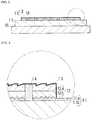
- FIG. 1 is a cross sectional view of a light emitting device 100 according to a first embodiment
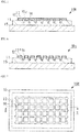
- FIG. 2 is a top view of a phosphor-containing member 10a (i.e., a view seen from a light emission surface side)
- FIG. 3 is a cross sectional view taken along the X-X line in FIG. 2
- FIG. 4 is an enlarged view of a region at the inside of the broken line frame in FIG. 3 .
- illustration of an optical film 13 is omitted for the sake of easy understanding of the configuration of the members.
- the light emitting device 100 includes a phosphor-containing member 10a and a light source 20 that is disposed at a location spaced away from the phosphor-containing member 10a and configured to irradiate light onto an upper surface of the phosphor portions 12 of the phosphor-containing member 10a.
- the phosphor-containing member 10a includes a base portion 11 made of a diffuse reflective ceramic, and a plurality of phosphor portions 12 each including a phosphor and being made of a ceramic. The plurality of phosphor portions 12 are spaced apart from each other and are disposed directly on an upper surface of the base portion 11.
- a conventional light emitting device includes a plurality of phosphor portions disposed on an upper surface of the base portion via a metal material.
- specular reflection easily occurs at metal materials. Therefore, a part of light that is emitted from the light source and has entered an interior of the phosphor portions proceeds downward, is specular-reflected by the metal material, and extracted to the outside of the phosphor portions without subjecting wavelength conversion.
- the blue light incident on the upper surfaces of the phosphor portions obliquely from a upper left side thereof tends to be reflected obliquely upward to a right side, so that the blue light tends to have high intensity when the upper surfaces of the phosphor portions are viewed obliquely from the upper right side.
- the fluorescence emitted from the phosphor portions is mainly emitted toward directly above the phosphor portions. Therefore, with the conventional light emitting device, color unevenness of emitted light tends to occur in the case where the phosphor-containing member is used in combination with a light source.
- the plurality of phosphor portions 12 made of a ceramic are arranged directly on the upper surface of the base portion 11 made of a diffuse reflective ceramic. Diffuse reflection (i.e., scattering reflection) occurs at a ceramic material more easily than at a metal material.
- first light light from the light source 20
- both the base portion 11 and the phosphor portions 12 are made of ceramic, which allows, even if the width of the phosphor portions 12 is reduced, the phosphor portions 12 to be easily prevented from being detached from the base portion 11.
- FIG. 1 shows a cross sectional view of a laser package as the light emitting device 100.
- the light emitting device 100 has a base 31 and a cover 32 bonded to the base 31, and the space defined by the base 31 and the cover 32 is a sealed space. At the inside of this space, a semiconductor laser element, which serve as the light source 20, and the phosphor-containing member 10a are disposed.
- the cover 32 includes a frame 32a made of metal or the like, and a light-transmissive part 32b made of glass or the like. The light-transmissive part 32b is arranged to close the opening provided to the frame 32a.
- the light emitting surface side of the light emitting device 100 i.e., an upper side of respective end surface views; for example, an upper side of FIG. 1
- the opposite side thereof i.e., a lower side of respective end views; for example, a lower side of FIG. 1
- the lower side the light emitting surface side of the light emitting device 100
- the opposite side thereof i.e., a lower side of respective end views; for example, a lower side of FIG. 1
- the semiconductor laser element as the light source 20 is mounted on the base 31 via a sub-mount 60 so that the optical axis of the first light is substantially parallel to the lower surface of the base 31.
- a prism 50 is disposed in the emission direction of the first light emitted laterally from the semiconductor laser element, and the first light is bent downward by the prism 50. Accordingly, the first light can be irradiated on the upper surfaces of the phosphor portions 12.
- a lens 40 is disposed between the light source 20 and the prism 50 in view of the spread angle of the first light. A converging lens or a collimating lens can be selected for the lens 40. In the case where the spread angle of the first light is small, a lens may not be provided.
- the area of a region of the phosphor-containing member 10a irradiated by the light from the light source 20 is larger than a total of the areas of the upper surfaces of two or more phosphor portions 12.
- spreading of the first light in the phosphor-containing member 10a can be reduced, so that emission with higher luminance can be obtained.
- the phosphor portions 12 are more likely to be detached due to the difference in the coefficient of thermal expansion between the phosphor portions 12 and the base portion 11, but with this embodiment, detachment of the phosphor portions 12 can be reduced.
- the region of the phosphor-containing member 10a irradiated with the light from the light source 20 preferably has an area of twice to 10,000 times, more preferably five times to and 5,000 times, and even more preferably at 100 times to 1000 times as large as the area of the upper surface of each of the phosphor portions 12.
- an area of twice as large as the area of the upper surface of each of the phosphor portions 12 or greater spreading of light in the phosphor-containing member 10a can be reduced, so that luminance can be easily increased.
- a size of each of the phosphor portions 12 may not be excessively reduced, which allows easy manufacturing of the phosphor-containing member 10a.
- the phosphor-containing member 10a in the present embodiment includes the base portion 11 disposed on an upper surface of a heat dissipation component 15, the plurality of the phosphor portions 12 disposed directly on an upper surface of the base portion 11, a light shielding portion 14 disposed between the phosphor portions 12, and an optical film 13 disposed on the upper surface of each of the phosphor portions 12 and the upper surface of the light shielding portion 14.
- the main constituent elements of the phosphor-containing member 10a will be described below.
- the base portion 11 is made of a diffuse reflective ceramic material, and a plurality of phosphor portions 12 are disposed thereon.
- the base portion 11 has a first region 11a in contact with the phosphor portions 12, and a second region 11b located below the first region 11a.
- the first region 11a has a reflectance with respect to light for exciting the phosphors (i.e., first light in the present embodiment) that is higher than that of the second region 11b.
- a material having a sintering temperature lower than the sintering temperature of the phosphor portions can be used for a material of the base portion 11 in a region in contact with the phosphor portions.
- Examples of a method of arranging the phosphor portions directly on the upper surface of the base portion include a method in which sintered body obtained by pre-firing as the phosphor portion is disposed on an upper surface of a ceramic powder, a constant pressure is applied, and the ceramic powder is further fired.
- the phosphor portions 12 are disposed directly on the upper surface of the base portion 11 by disposing, a sintered body of a ceramic material that has been fired at high temperature (corresponding to the "second region 11b" discussed below; hereinafter referred to as the "second member"), a ceramic powder (subsequently becoming the "first region 11 a"; hereinafter referred to as the "first member"), and another sintered body to be the phosphor portions 12, in this order starting from a lower side, and then performing firing. With the second member that has been fired at a high temperature, strength of the base portion 11 can be ensured.
- the firing temperature at this time is a temperature that allows the second member and the phosphor portions 12 to be joined together via the first member, so the firing temperature can be a relatively low temperature. Therefore, in the present embodiment, the first region 11a allows for ensuring good light reflection, while the second region 11b allows for ensuring good strength.
- the base portion 11 having uniform diffuse reflection and strength by disposing sintered phosphor portions on the upper surface of a ceramic powder and performing firing under pressure.
- the main component of each of the first region 11a and the second region 11b is aluminum oxide. More specifically, first, aluminum oxide particles are fired at a high temperature to accelerate grain growth, so that the second region 11b having high light-transmittance and great strength is formed. Next, aluminum oxide particles are disposed on the upper surface of the second region 11b, and the aluminum oxide particles are fired at a firing temperature lower than the firing temperature of the second region 11b. This allows for forming a base portion 11 having a first region 11a with high diffuse reflection, albeit having lower strength than in the second region 11b.
- aluminum oxide and the like may be the main component of the base portion 11, and the base portion 11 may be made of materials with the same reflectance as an entirety of the base portion 11.
- a height between the lower surface of the base portion 11 and the upper surface of the base portion 11 is preferably in the range of 200 ⁇ m to 2000 ⁇ m, and more preferably in the range of 400 ⁇ m to 1300 ⁇ m. With a height of 200 ⁇ m or more, good strength of the base portion 11 can be ensured, and with a height of 2000 ⁇ m or less, heat dissipation from the phosphor portions 12 can be improved.
- the phosphor portions 12 are made of a ceramic and contain a phosphor.
- the phosphor portions 12 are made of a phosphor and an additive. More specifically, in this embodiment, the phosphor portions 12 are made of a YAG (yttrium aluminum garnet) phosphor and an additive containing aluminum oxide. This allows the concentration of the phosphor in the phosphor portions 12 to be appropriately adjusted. Alternatively, the phosphor portions 12 made only of a phosphor may be used.
- a single type of phosphor or two or more types of phosphors that are mixed can be used for the phosphor.
- selecting a phosphor for emitting yellow light or selecting a phosphor for emitting yellow light and a phosphor for emitting red light allows for obtaining white light, which is mixture of light with these colors.
- a phosphor for emitting yellow light includes at least one of YAG and LAG.
- a phosphor for emitting red light includes at least one of CASN and BESN.
- the additives include at least one of aluminum oxide and yttrium oxide.
- a phosphor particle of the phosphor preferably has a diameter smaller than one side of the phosphor portion in a top view. This allows for easily scattering light at an inside of the phosphor portions 12.
- the upper and lower surfaces of each of the phosphor portions 12 are rough surfaces. With the upper surfaces of the phosphor portions 12 that are roughened, the first light can be easily incident on the phosphor portions 12. Also, with the lower surfaces of the phosphor portions 12 that are roughened, the first light can be easily scattered by the lower surfaces of the phosphor portions 12, so that color unevenness of light from the light emitting device 100 can be easily reduced.
- the upper and lower surfaces of the phosphor portions 12 are rough surfaces, but alternatively, either the upper surfaces or the lower surfaces of the phosphor portions 12 may be rough surfaces, or the upper and lower surfaces of the phosphor portions 12 may be substantially flat surfaces.
- a sintered body that is to serve as the phosphor portions and has upper and lower surfaces are prepared, the sintered body (i.e., phosphor portions) thus prepared is disposed on an upper surface of a ceramic powder disposed on an upper surface of a ceramic sintered body, and firing is then performed, which allows for obtaining the phosphor portions 12 with roughened upper and lower surfaces.
- each of the phosphor portions 12 has a first region 12a and a second region 12b located below the first region 12a.
- the first region 12a has a reflectance with respect to light for exciting the phosphor lower than the reflectance of the second region 12b with respect to light for exciting the phosphor.
- reflection of the first light on the upper surface of the first region 12a can be reduced, so the first light is more likely to be incident at the inside of the phosphor portions 12.
- a single crystal phosphor is used for the first region 12a, and a sintered body of a phosphor and an additive is used for the second region 12b. This arrangement allows the grain boundary of the first region 12a to be reduced compared with the grain boundary of the second region 12b, so that the above-described effect can be more easily obtained.
- the phosphor portions 12 has a substantially square shape when viewed from above. This allows for easily forming the phosphor portions 12.
- the phosphor portions 12 may have any appropriate shape, and may have a substantially circular shape or the like when viewed from above.
- each of sides of the lower surface of each of the phosphor portions 12 preferably has a length of 5 ⁇ m to 500 ⁇ m, more preferably 10 ⁇ m to 200 ⁇ m, and even more preferably 15 ⁇ m to 50 ⁇ m. With the length of 5 ⁇ m or greater, detachment of the phosphor portions 12 can be easily prevented, and with the length of 500 ⁇ m or smaller, decrease in the luminance of the light emitting device can be easily prevented.
- the "length of each of sides of the lower surface of each of the phosphor portions 12" in the present specification refers to a length of a straight line connecting the two ends of the lower surface in a cross sectional view of each of the phosphor portions 12.
- each of the phosphor portions 12 preferably has a thickness (i.e., the distance between the upper surfaces of the phosphor portions 12 and the lower surfaces of the phosphor portions 12) in a range of 30 ⁇ m to 300 ⁇ m, and more preferably 50 ⁇ m to 100 ⁇ m. With the thickness of 30 ⁇ m or greater, the phosphor can be easily contained in the phosphor portions 12, and therefore wavelength conversion of the first light can be facilitated. With the thickness of 300 ⁇ m or smaller, breakage of the phosphor portions 12 can be easily prevented.
- the distance between adjacent phosphor portions 12 is preferably in a range of 1 ⁇ m to 100 ⁇ m, and more preferably 3 ⁇ m to 10 ⁇ m. With the distance of 1 ⁇ m or greater, gaps between the phosphor portions 12 can be easily formed, and with the distance of 100 ⁇ m or smaller, the area of the upper surfaces of the phosphor portions 12 included in the region irradiated with the first light can be increased.
- Examples of a method of forming a plurality of phosphor portions 12 includes, arranging a fluorescent plate directly on the upper surface of the base portion 11 and then forming grooves from the upper surface side of the fluorescent plate by laser working. Forming the phosphor portions 12 by laser processing allows the distance between the adjacent phosphor portions 12 to be uniform easily.
- a plurality of phosphor portions 12 are formed by laser processing, but alternatively, a plurality of phosphor portions 12 that have been separated may be bonded to a single base portion 11.
- a light shielding portion 14 is disposed between adjacent phosphor portions 12. This allows the light advancing toward lateral surfaces of the phosphor portions 12 to be reflected, so that decrease in luminance can be easily prevented.
- a known light reflecting material such as a metal material can be used for the light shielding portion 14. Also, the light shielding portion 14 may not be provided.
- An optical film 13 can be disposed on the upper surfaces of the phosphor portions 12.
- an antireflective coating (AR coating) or the like can be used. This allows the first light to be easily incident on the phosphor portions 12.
- the optical film 13 is disposed on outermost lateral surfaces of the phosphor portions 12, the upper surfaces of the phosphor portions 12, and the upper surface of the light shielding portion 14.
- the base portion 11 is bonded to the heat dissipation component 15. This allows for improving heat dissipation from the base portion 11.
- a metal whose main component is copper, tungsten, molybdenum, etc., a ceramic having better heat dissipation than the base portion 11, or the like can be used.
- the heat dissipation component 15 and the base portion 11 can be bonded via a bonding material or the like, or can be performed without a bonding material.
- the base portion 11 is bonded to the base 31 via the heat dissipation component 15, but alternatively, the base portion 11 may be bonded directly to the base 31 without interposing the heat dissipation component 15 therebetween.
- FIG. 5 is a cross sectional view of a phosphor-containing member 10b according to a second embodiment.
- the phosphor-containing member 10b is substantially the same as the configuration the phosphor-containing member 10a described above, except for the configuration described below.
- the phosphor-containing member 10b may be used instead of the phosphor-containing member 10a.
- the base portion 11 includes a plurality of projecting portions 11c, and one phosphor portion 12 is disposed with respect to each of the projecting portions 11c.
- This structure allows for reducing lateral propagation of light entered the base portion 11 from the phosphor portions 12, so that luminance of emitted light can be easily increased.
- each of the phosphor portions 12 has a thickness in an up-down direction (upper-lower direction) smaller than the thickness of respective one of the projecting portions 11c (i.e., the length in the up-down direction in FIG. 5 ). This allows for improving light extract efficiency while reducing color unevenness of light emitted from the light emitting device 100.
- Each of the projecting portions 11c preferably has a thickness in the range of 100 ⁇ m to 500 ⁇ m, and more preferably 200 ⁇ m to 400 ⁇ m. With the thickness of 100 ⁇ m or greater, lateral propagation of light inside the base portion 11 can be easily prevented even if the thickness of the phosphor portions 12 is reduced. With the thickness of 500 ⁇ m or smaller, decrease in heat dissipation from the phosphor portions 12 can be easily prevented.
- FIG. 6 is a cross sectional view of a phosphor-containing member 10c according to a third embodiment.
- the phosphor-containing member 10c is substantially the same as the configuration described for the phosphor-containing member 10a except for the configuration described below.
- the phosphor-containing member 10c can be used instead of the phosphor-containing member 10a.
- the base portion 11 includes a plurality of projecting portions 11c, and one phosphor portion 12 is disposed with respect to each of the projecting portions 11c. Also, at least one lateral surface of each of the projecting portions 11c and at least one lateral surface of each of the phosphor portions 12 are sloped such that a width of each of the projecting portions 11c and a width of respective one of the phosphor portions 12 are reduced upward from a lower side as viewed in FIG. 6 .
- each of the projecting portions 11c and at least one lateral surface of each of the phosphor portions 12 are sloped such that a width of each of the projecting portions 11c and a width of respective one of the phosphor portions 12 are reduced upward from a lower side as viewed in the right-left direction in FIG. 6 , namely as viewed along the X-X line, for example, shown in FIG. 2 .
- the light shielding portion 14 is not disposed between the phosphor portions 12.
- FIG. 7 is a top view of a phosphor-containing member 10d according to a fourth embodiment
- FIG. 8 is a cross sectional view taken along the X-X line in FIG. 7 .
- the phosphor-containing member 10d is substantially the same as the configuration of the phosphor-containing member 10a described above except for the configuration described below. In the first embodiment of light emitting device, the phosphor-containing member 10d may be used instead of the phosphor-containing member 10a.
- the base portion 11 includes a plurality of projecting portions 11c, and one phosphor portion 12 is disposed with respect to each of the projecting portions 11c. Also, when viewed from the upper surface side, the area of each of the phosphor portions 12 and the area of the base portion 11 are the same. Also, when viewed from the upper surface side, the outermost periphery of an entirety of the phosphor portions 12 corresponds to the outermost periphery of the base portion 11. Further, the phosphor-containing member 10d includes a plurality of phosphor portions 12 and one continuous phosphor portion 12 that surrounds the plurality of phosphor portions 12 when viewed from the upper surface side.
- the size of the fluorescent plate is larger than the region irradiated with the first light
- forming grooves by laser processing in only the region irradiated with the first light allows for reducing time for producing the phosphor-containing member.
- the area of the fluorescent plate is smaller than the area of the base portion 11 when viewed from the upper surface side, if the area of the fluorescent plate is larger than the region irradiated with the first light, grooves may be formed in the fluorescent plate by laser processing only in the region irradiated with the first light.
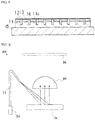
- FIG. 9 is a schematic view of the laser module as a light emitting device 200 according to the fifth embodiment.
- the light emitting device 200 includes a laser package, which serves as the light source 20, a phosphor-containing member 10a for converting the wavelength of a part of the first light, and an optical system 80, such as a lens or the like, on which light from the phosphor-containing member 10a is incident.
- the light emitted from the laser package is irradiated to the phosphor-containing member 10a through the light guide member 71.
- light from the phosphor-containing member 10a that has passed through the optical system 80 is extracted to the outside through a window 90, for example.
- the configuration of the phosphor-containing member 10a is substantially the same as the configuration of the light-emitting device 100 described above.
- a laser package or the like is disposed so that the first light emitted from the semiconductor laser element included in the laser package is incident on the upper surface of each of the phosphor portions 12. That is, a laser package or the like is disposed so that the first light is emitted in a direction different from the light extracting direction of the light emitting device (i.e., toward an upper side in FIG. 9 ). With this arrangement, even if the phosphor-containing member 10a is detached, extraction of the first light directly to the outside can be easily prevented. In FIG. 9 , a laser package or the like is disposed so that the first light is incident obliquely to the upper surfaces of the phosphor portions 12. With this arrangement, a member for shielding light that advances from the phosphor-containing member 10a toward the laser package may not be disposed.
- an optical fiber can be used, for example.
- the phosphor-containing member 10a can be irradiated with the first light while reducing spread of the beam diameter of the first light.
- the laser package may alternatively be disposed so that the light from the laser package is directly irradiated to the upper surface of each of the phosphor portions 12, without using the light guide member 71.
- the phosphor-containing member 10b, the phosphor-containing member 10c, or the phosphor-containing member 10d may be used instead of the phosphor-containing member 10a.
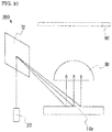
- FIG. 10 is a schematic view of the laser module as a light emitting device 300 according to a sixth embodiment.
- the light emitting device 300 is substantially the same as the configuration of the light emitting device 200 described above except for the configuration described below.
- the light emitting device 300 includes a light reflecting mechanism 72 configured to reflect the first light toward the phosphor-containing member 10a on an optical path of the first light.
- the light reflecting mechanism 72 includes, for example, a digital micromirror device having a large number of mirror surfaces. With this arrangement, a region in the phosphor-containing member 10a to be irradiated with the first light can be adjusted. According to the present embodiment, the same effect as in the light emitting device of the fifth embodiment can be obtained.
- the phosphor-containing member and the light emitting device according to respective embodiments can be applied for vehicle installation, illumination and the like.
- the phosphor-containing member 10a, 10b, 10c, 10d can be obtained that allows for reducing color unevenness of emitted light and suppressing detachment of the phosphor portions 12, in the case where the phosphor-containing member 10a, 10b, 10c, 10d is used in combination with the light source 20.
Landscapes
- Engineering & Computer Science (AREA)
- General Engineering & Computer Science (AREA)
- Physics & Mathematics (AREA)
- Chemical & Material Sciences (AREA)
- Optics & Photonics (AREA)
- Spectroscopy & Molecular Physics (AREA)
- Microelectronics & Electronic Packaging (AREA)
- Inorganic Chemistry (AREA)
- Materials Engineering (AREA)
- Organic Chemistry (AREA)
- Condensed Matter Physics & Semiconductors (AREA)
- General Physics & Mathematics (AREA)
- Electromagnetism (AREA)
- Ceramic Engineering (AREA)
- Semiconductor Lasers (AREA)
- Optical Filters (AREA)
Abstract
Description
- The present invention relates to a phosphor-containing member and a light emitting device containing the phosphor-containing member.
- In the light source device discussed in
JP2012-129135A - One object of the present disclosure is to provide a phosphor-containing member which can be obtained that reduces color unevenness and makes it easier to suppress detachment of the phosphor portion in the case where the phosphor-containing member is used in combination with a light source.
- A certain embodiment of the present disclosure includes a phosphor-containing member which includes a base portion made of a diffuse reflective ceramic, and a plurality of phosphor portions each containing a phosphor and made of a ceramic, and the plurality of phosphor portions are disposed directly on an upper surface of the base portion and spaced apart from each other.
- Another embodiment of the present disclosure includes a light emitting device which includes the phosphor-containing member as described above and a light source that is disposed at a location spaced apart from the phosphor-containing member and configured to irradiate light for exciting the phosphors to an upper surface of the base portions.
-
-
FIG. 1 is a cross sectional view of a light emitting device according to a first embodiment; -
FIG. 2 is a top view of a phosphor-containing member; -
FIG. 3 is a cross sectional view taken along the X-X line inFIG. 2 ; -
FIG. 4 is an enlarged view of a region at the inside of the broken line frame inFIG. 3 ; -
FIG. 5 is a cross sectional view of a light emitting device according to a second embodiment; -
FIG. 6 is a cross sectional view of a light emitting device according to a third embodiment; -
FIG. 7 is a top view of a phosphor-containing member according to a fourth embodiment; -
FIG. 8 is a cross sectional view taken along the X-X line inFIG. 7 ; -
FIG. 9 is a schematic view of a light emitting device according to a fifth embodiment; and -
FIG. 10 is a schematic view of a light emitting device according to a sixth embodiment. - Certain embodiments of the present invention will be described below with reference to the accompanying drawings. In the embodiments in the below are intended to embody the technological concept of the present invention, and are not intended to limit the scope of the present invention. Also, the sizes and the positional relationship of the members described in the drawings may be exaggerated for the sake of clarity.
-
FIG. 1 is a cross sectional view of alight emitting device 100 according to a first embodiment,FIG. 2 is a top view of a phosphor-containingmember 10a (i.e., a view seen from a light emission surface side),FIG. 3 is a cross sectional view taken along the X-X line inFIG. 2 , andFIG. 4 is an enlarged view of a region at the inside of the broken line frame inFIG. 3 . InFIG. 2 , illustration of anoptical film 13 is omitted for the sake of easy understanding of the configuration of the members. - The
light emitting device 100 includes a phosphor-containingmember 10a and alight source 20 that is disposed at a location spaced away from the phosphor-containingmember 10a and configured to irradiate light onto an upper surface of thephosphor portions 12 of the phosphor-containingmember 10a. The phosphor-containingmember 10a includes abase portion 11 made of a diffuse reflective ceramic, and a plurality ofphosphor portions 12 each including a phosphor and being made of a ceramic. The plurality ofphosphor portions 12 are spaced apart from each other and are disposed directly on an upper surface of thebase portion 11. - With this arrangement, it is possible to obtain a phosphor-containing member with which color unevenness of emitted light can be reduced and in which the phosphor portions are less likely to detached.
- A conventional light emitting device includes a plurality of phosphor portions disposed on an upper surface of the base portion via a metal material. However, specular reflection easily occurs at metal materials. Therefore, a part of light that is emitted from the light source and has entered an interior of the phosphor portions proceeds downward, is specular-reflected by the metal material, and extracted to the outside of the phosphor portions without subjecting wavelength conversion. For example, in the case where blue light is emitted from the light source, the blue light incident on the upper surfaces of the phosphor portions obliquely from a upper left side thereof tends to be reflected obliquely upward to a right side, so that the blue light tends to have high intensity when the upper surfaces of the phosphor portions are viewed obliquely from the upper right side. Meanwhile, the fluorescence emitted from the phosphor portions is mainly emitted toward directly above the phosphor portions. Therefore, with the conventional light emitting device, color unevenness of emitted light tends to occur in the case where the phosphor-containing member is used in combination with a light source. Also, in order to suppress a decrease in luminance due to light scattering, an attempt to reduce the width of the phosphor portions has been made in conventional light emitting devices, but if the width of the phosphor portions is reduced, the contact area between the phosphor portions and the metallic material is also reduced. Because a metal material has a thermal expansion coefficient higher than that of ceramics, thermal expansion and contraction are repeated due to heat generated in the phosphor portions and radiated to the bonding material made of a metal material, which may cause detachment of the phosphor portions more easily.
- By contrast, in the phosphor-containing
member 10a according to the present embodiment, the plurality ofphosphor portions 12 made of a ceramic are arranged directly on the upper surface of thebase portion 11 made of a diffuse reflective ceramic. Diffuse reflection (i.e., scattering reflection) occurs at a ceramic material more easily than at a metal material. With thephosphor portions 12 disposed directly on thebase portion 11, light from the light source 20 (hereinafter referred to as "first light") is more likely to be reflected while being diffused at the upper surface of thebase portion 11, so that color unevenness of light emitted from thelight emitting device 100 can be reduced. Also, in the present embodiment, both thebase portion 11 and thephosphor portions 12 are made of ceramic, which allows, even if the width of thephosphor portions 12 is reduced, thephosphor portions 12 to be easily prevented from being detached from thebase portion 11. -
FIG. 1 shows a cross sectional view of a laser package as thelight emitting device 100. Thelight emitting device 100 has abase 31 and acover 32 bonded to thebase 31, and the space defined by thebase 31 and thecover 32 is a sealed space. At the inside of this space, a semiconductor laser element, which serve as thelight source 20, and the phosphor-containingmember 10a are disposed. Thecover 32 includes aframe 32a made of metal or the like, and a light-transmissive part 32b made of glass or the like. The light-transmissive part 32b is arranged to close the opening provided to theframe 32a. In the present specification, the light emitting surface side of the light emitting device 100 (i.e., an upper side of respective end surface views; for example, an upper side ofFIG. 1 ) is referred to as the "upper side", and the opposite side thereof (i.e., a lower side of respective end views; for example, a lower side ofFIG. 1 ) is referred to as the "lower side". - In the present embodiment, the semiconductor laser element as the
light source 20 is mounted on thebase 31 via asub-mount 60 so that the optical axis of the first light is substantially parallel to the lower surface of thebase 31. Aprism 50 is disposed in the emission direction of the first light emitted laterally from the semiconductor laser element, and the first light is bent downward by theprism 50. Accordingly, the first light can be irradiated on the upper surfaces of thephosphor portions 12. Also, in the present embodiment, alens 40 is disposed between thelight source 20 and theprism 50 in view of the spread angle of the first light. A converging lens or a collimating lens can be selected for thelens 40. In the case where the spread angle of the first light is small, a lens may not be provided. - As shown in
FIG. 2 , in the present embodiment, in a top view, the area of a region of the phosphor-containingmember 10a irradiated by the light from thelight source 20 is larger than a total of the areas of the upper surfaces of two ormore phosphor portions 12. With this structure, spreading of the first light in the phosphor-containingmember 10a can be reduced, so that emission with higher luminance can be obtained. Furthermore, in the case where each of thephosphor portions 12 has a small area, thephosphor portions 12 are more likely to be detached due to the difference in the coefficient of thermal expansion between thephosphor portions 12 and thebase portion 11, but with this embodiment, detachment of thephosphor portions 12 can be reduced. - The region of the phosphor-containing
member 10a irradiated with the light from thelight source 20 preferably has an area of twice to 10,000 times, more preferably five times to and 5,000 times, and even more preferably at 100 times to 1000 times as large as the area of the upper surface of each of thephosphor portions 12. With an area of twice as large as the area of the upper surface of each of thephosphor portions 12 or greater, spreading of light in the phosphor-containingmember 10a can be reduced, so that luminance can be easily increased. Also, with an area of 10,000 times as large as the upper surface of each of thephosphor portions 12 or smaller, a size of each of thephosphor portions 12 may not be excessively reduced, which allows easy manufacturing of the phosphor-containingmember 10a. - As shown in
FIG. 3 , the phosphor-containingmember 10a in the present embodiment includes thebase portion 11 disposed on an upper surface of aheat dissipation component 15, the plurality of thephosphor portions 12 disposed directly on an upper surface of thebase portion 11, alight shielding portion 14 disposed between thephosphor portions 12, and anoptical film 13 disposed on the upper surface of each of thephosphor portions 12 and the upper surface of thelight shielding portion 14. The main constituent elements of the phosphor-containingmember 10a will be described below. - The
base portion 11 is made of a diffuse reflective ceramic material, and a plurality ofphosphor portions 12 are disposed thereon. - In the present embodiment, as shown in
FIG. 4 , thebase portion 11 has afirst region 11a in contact with thephosphor portions 12, and a second region 11b located below thefirst region 11a. Thefirst region 11a has a reflectance with respect to light for exciting the phosphors (i.e., first light in the present embodiment) that is higher than that of the second region 11b. With this arrangement, good light reflection can be ensured in thefirst region 11a, while good strength can be ensured also in the second region 11b. This will be described below in detail. - In order to reduce deterioration of the phosphors due to heat, a material having a sintering temperature lower than the sintering temperature of the phosphor portions can be used for a material of the
base portion 11 in a region in contact with the phosphor portions. Examples of a method of arranging the phosphor portions directly on the upper surface of the base portion include a method in which sintered body obtained by pre-firing as the phosphor portion is disposed on an upper surface of a ceramic powder, a constant pressure is applied, and the ceramic powder is further fired. At this time, in order to increase the strength of the base portion, it is necessary to fire the ceramic powder at a high temperature for a relatively long time, but heating for a relatively long time at high temperature causes grain-growth of the ceramic powder, which may lead to increase in optical transmittance of the base portion, so that scattering reflectivity of the base portion may be decreased. In view of this, in the present embodiment, thephosphor portions 12 are disposed directly on the upper surface of thebase portion 11 by disposing, a sintered body of a ceramic material that has been fired at high temperature (corresponding to the "second region 11b" discussed below; hereinafter referred to as the "second member"), a ceramic powder (subsequently becoming the "first region 11 a"; hereinafter referred to as the "first member"), and another sintered body to be thephosphor portions 12, in this order starting from a lower side, and then performing firing. With the second member that has been fired at a high temperature, strength of thebase portion 11 can be ensured. Accordingly, the firing temperature at this time is a temperature that allows the second member and thephosphor portions 12 to be joined together via the first member, so the firing temperature can be a relatively low temperature. Therefore, in the present embodiment, thefirst region 11a allows for ensuring good light reflection, while the second region 11b allows for ensuring good strength. Alternatively, for example, thebase portion 11 having uniform diffuse reflection and strength by disposing sintered phosphor portions on the upper surface of a ceramic powder and performing firing under pressure. - In the present embodiment, the main component of each of the
first region 11a and the second region 11b is aluminum oxide. More specifically, first, aluminum oxide particles are fired at a high temperature to accelerate grain growth, so that the second region 11b having high light-transmittance and great strength is formed. Next, aluminum oxide particles are disposed on the upper surface of the second region 11b, and the aluminum oxide particles are fired at a firing temperature lower than the firing temperature of the second region 11b. This allows for forming abase portion 11 having afirst region 11a with high diffuse reflection, albeit having lower strength than in the second region 11b. Alternatively, aluminum oxide and the like may be the main component of thebase portion 11, and thebase portion 11 may be made of materials with the same reflectance as an entirety of thebase portion 11. - A height between the lower surface of the
base portion 11 and the upper surface of thebase portion 11 is preferably in the range of 200 µm to 2000 µm, and more preferably in the range of 400 µm to 1300 µm. With a height of 200 µm or more, good strength of thebase portion 11 can be ensured, and with a height of 2000 µm or less, heat dissipation from thephosphor portions 12 can be improved. - The
phosphor portions 12 are made of a ceramic and contain a phosphor. In the present embodiment, thephosphor portions 12 are made of a phosphor and an additive. More specifically, in this embodiment, thephosphor portions 12 are made of a YAG (yttrium aluminum garnet) phosphor and an additive containing aluminum oxide. This allows the concentration of the phosphor in thephosphor portions 12 to be appropriately adjusted. Alternatively, thephosphor portions 12 made only of a phosphor may be used. - A single type of phosphor or two or more types of phosphors that are mixed can be used for the phosphor. In the case where the first light is blue light, selecting a phosphor for emitting yellow light or selecting a phosphor for emitting yellow light and a phosphor for emitting red light allows for obtaining white light, which is mixture of light with these colors. For example, a phosphor for emitting yellow light includes at least one of YAG and LAG. For example, a phosphor for emitting red light includes at least one of CASN and BESN. For example, the additives include at least one of aluminum oxide and yttrium oxide. A phosphor particle of the phosphor preferably has a diameter smaller than one side of the phosphor portion in a top view. This allows for easily scattering light at an inside of the
phosphor portions 12. - As shown in
FIG. 4 , in the present embodiment, the upper and lower surfaces of each of thephosphor portions 12 are rough surfaces. With the upper surfaces of thephosphor portions 12 that are roughened, the first light can be easily incident on thephosphor portions 12. Also, with the lower surfaces of thephosphor portions 12 that are roughened, the first light can be easily scattered by the lower surfaces of thephosphor portions 12, so that color unevenness of light from thelight emitting device 100 can be easily reduced. In the present embodiment, the upper and lower surfaces of thephosphor portions 12 are rough surfaces, but alternatively, either the upper surfaces or the lower surfaces of thephosphor portions 12 may be rough surfaces, or the upper and lower surfaces of thephosphor portions 12 may be substantially flat surfaces. In the present embodiment, a sintered body that is to serve as the phosphor portions and has upper and lower surfaces are prepared, the sintered body (i.e., phosphor portions) thus prepared is disposed on an upper surface of a ceramic powder disposed on an upper surface of a ceramic sintered body, and firing is then performed, which allows for obtaining thephosphor portions 12 with roughened upper and lower surfaces. - In the present embodiment, each of the
phosphor portions 12 has afirst region 12a and a second region 12b located below thefirst region 12a. Thefirst region 12a has a reflectance with respect to light for exciting the phosphor lower than the reflectance of the second region 12b with respect to light for exciting the phosphor. With this arrangement, reflection of the first light on the upper surface of thefirst region 12a can be reduced, so the first light is more likely to be incident at the inside of thephosphor portions 12. For example, a single crystal phosphor is used for thefirst region 12a, and a sintered body of a phosphor and an additive is used for the second region 12b. This arrangement allows the grain boundary of thefirst region 12a to be reduced compared with the grain boundary of the second region 12b, so that the above-described effect can be more easily obtained. - In the present embodiment, the
phosphor portions 12 has a substantially square shape when viewed from above. This allows for easily forming thephosphor portions 12. Thephosphor portions 12 may have any appropriate shape, and may have a substantially circular shape or the like when viewed from above. - In the present embodiment, each of sides of the lower surface of each of the
phosphor portions 12 preferably has a length of 5 µm to 500 µm, more preferably 10 µm to 200 µm, and even more preferably 15 µm to 50 µm. With the length of 5 µm or greater, detachment of thephosphor portions 12 can be easily prevented, and with the length of 500 µm or smaller, decrease in the luminance of the light emitting device can be easily prevented. The "length of each of sides of the lower surface of each of thephosphor portions 12" in the present specification refers to a length of a straight line connecting the two ends of the lower surface in a cross sectional view of each of thephosphor portions 12. Also, each of thephosphor portions 12 preferably has a thickness (i.e., the distance between the upper surfaces of thephosphor portions 12 and the lower surfaces of the phosphor portions 12) in a range of 30 µm to 300 µm, and more preferably 50 µm to 100 µm. With the thickness of 30 µm or greater, the phosphor can be easily contained in thephosphor portions 12, and therefore wavelength conversion of the first light can be facilitated. With the thickness of 300 µm or smaller, breakage of thephosphor portions 12 can be easily prevented. - The distance between
adjacent phosphor portions 12 is preferably in a range of 1 µm to 100 µm, and more preferably 3 µm to 10 µm. With the distance of 1 µm or greater, gaps between thephosphor portions 12 can be easily formed, and with the distance of 100 µm or smaller, the area of the upper surfaces of thephosphor portions 12 included in the region irradiated with the first light can be increased. - Examples of a method of forming a plurality of
phosphor portions 12 includes, arranging a fluorescent plate directly on the upper surface of thebase portion 11 and then forming grooves from the upper surface side of the fluorescent plate by laser working. Forming thephosphor portions 12 by laser processing allows the distance between theadjacent phosphor portions 12 to be uniform easily. In the present embodiment, a plurality ofphosphor portions 12 are formed by laser processing, but alternatively, a plurality ofphosphor portions 12 that have been separated may be bonded to asingle base portion 11. - In the present embodiment, a
light shielding portion 14 is disposed betweenadjacent phosphor portions 12. This allows the light advancing toward lateral surfaces of thephosphor portions 12 to be reflected, so that decrease in luminance can be easily prevented. A known light reflecting material such as a metal material can be used for thelight shielding portion 14. Also, thelight shielding portion 14 may not be provided. - An
optical film 13 can be disposed on the upper surfaces of thephosphor portions 12. For theoptical film 13, an antireflective coating (AR coating) or the like can be used. This allows the first light to be easily incident on thephosphor portions 12. In the present embodiment, theoptical film 13 is disposed on outermost lateral surfaces of thephosphor portions 12, the upper surfaces of thephosphor portions 12, and the upper surface of thelight shielding portion 14. - In the present embodiment, the
base portion 11 is bonded to theheat dissipation component 15. This allows for improving heat dissipation from thebase portion 11. For theheat dissipation component 15, a metal whose main component is copper, tungsten, molybdenum, etc., a ceramic having better heat dissipation than thebase portion 11, or the like can be used. Theheat dissipation component 15 and thebase portion 11 can be bonded via a bonding material or the like, or can be performed without a bonding material. In this embodiment, thebase portion 11 is bonded to thebase 31 via theheat dissipation component 15, but alternatively, thebase portion 11 may be bonded directly to thebase 31 without interposing theheat dissipation component 15 therebetween. -
FIG. 5 is a cross sectional view of a phosphor-containingmember 10b according to a second embodiment. The phosphor-containingmember 10b is substantially the same as the configuration the phosphor-containingmember 10a described above, except for the configuration described below. In thelight emitting device 100 of the first embodiment, the phosphor-containingmember 10b may be used instead of the phosphor-containingmember 10a. - In the phosphor-containing
member 10b, thebase portion 11 includes a plurality of projectingportions 11c, and onephosphor portion 12 is disposed with respect to each of the projectingportions 11c. This structure allows for reducing lateral propagation of light entered thebase portion 11 from thephosphor portions 12, so that luminance of emitted light can be easily increased. - In the present embodiment, each of the
phosphor portions 12 has a thickness in an up-down direction (upper-lower direction) smaller than the thickness of respective one of the projectingportions 11c (i.e., the length in the up-down direction inFIG. 5 ). This allows for improving light extract efficiency while reducing color unevenness of light emitted from thelight emitting device 100. Each of the projectingportions 11c preferably has a thickness in the range of 100 µm to 500 µm, and more preferably 200 µm to 400 µm. With the thickness of 100 µm or greater, lateral propagation of light inside thebase portion 11 can be easily prevented even if the thickness of thephosphor portions 12 is reduced. With the thickness of 500 µm or smaller, decrease in heat dissipation from thephosphor portions 12 can be easily prevented. -
FIG. 6 is a cross sectional view of a phosphor-containingmember 10c according to a third embodiment. The phosphor-containingmember 10c is substantially the same as the configuration described for the phosphor-containingmember 10a except for the configuration described below. In the first embodiment of light emitting device, the phosphor-containingmember 10c can be used instead of the phosphor-containingmember 10a. - In the phosphor-containing
member 10c, thebase portion 11 includes a plurality of projectingportions 11c, and onephosphor portion 12 is disposed with respect to each of the projectingportions 11c. Also, at least one lateral surface of each of the projectingportions 11c and at least one lateral surface of each of thephosphor portions 12 are sloped such that a width of each of the projectingportions 11c and a width of respective one of thephosphor portions 12 are reduced upward from a lower side as viewed inFIG. 6 . Moreover, at least one lateral surface of each of the projectingportions 11c and at least one lateral surface of each of thephosphor portions 12 are sloped such that a width of each of the projectingportions 11c and a width of respective one of thephosphor portions 12 are reduced upward from a lower side as viewed in the right-left direction inFIG. 6 , namely as viewed along the X-X line, for example, shown inFIG. 2 . Furthermore, thelight shielding portion 14 is not disposed between thephosphor portions 12. With the lateral surfaces of thephosphor portions 12 sloped such that a width of each of the projectingportions 11c and a width of each of thephosphor portions 12 are reduced upward from a lower side, light advancing toward the outside from the lateral surfaces of thephosphor portions 12 can be easily extracted upward. -
FIG. 7 is a top view of a phosphor-containingmember 10d according to a fourth embodiment, andFIG. 8 is a cross sectional view taken along the X-X line inFIG. 7 . The phosphor-containingmember 10d is substantially the same as the configuration of the phosphor-containingmember 10a described above except for the configuration described below. In the first embodiment of light emitting device, the phosphor-containingmember 10d may be used instead of the phosphor-containingmember 10a. - With the phosphor-containing
member 10d, thebase portion 11 includes a plurality of projectingportions 11c, and onephosphor portion 12 is disposed with respect to each of the projectingportions 11c. Also, when viewed from the upper surface side, the area of each of thephosphor portions 12 and the area of thebase portion 11 are the same. Also, when viewed from the upper surface side, the outermost periphery of an entirety of thephosphor portions 12 corresponds to the outermost periphery of thebase portion 11. Further, the phosphor-containingmember 10d includes a plurality ofphosphor portions 12 and onecontinuous phosphor portion 12 that surrounds the plurality ofphosphor portions 12 when viewed from the upper surface side. In the case where the size of the fluorescent plate is larger than the region irradiated with the first light, forming grooves by laser processing in only the region irradiated with the first light allows for reducing time for producing the phosphor-containing member. Even in the case where the area of the fluorescent plate is smaller than the area of thebase portion 11 when viewed from the upper surface side, if the area of the fluorescent plate is larger than the region irradiated with the first light, grooves may be formed in the fluorescent plate by laser processing only in the region irradiated with the first light. -
FIG. 9 is a schematic view of the laser module as alight emitting device 200 according to the fifth embodiment. As shown inFIG. 9 , thelight emitting device 200 includes a laser package, which serves as thelight source 20, a phosphor-containingmember 10a for converting the wavelength of a part of the first light, and anoptical system 80, such as a lens or the like, on which light from the phosphor-containingmember 10a is incident. The light emitted from the laser package is irradiated to the phosphor-containingmember 10a through thelight guide member 71. Also, light from the phosphor-containingmember 10a that has passed through theoptical system 80 is extracted to the outside through awindow 90, for example. The configuration of the phosphor-containingmember 10a is substantially the same as the configuration of the light-emittingdevice 100 described above. - In the present embodiment, a laser package or the like is disposed so that the first light emitted from the semiconductor laser element included in the laser package is incident on the upper surface of each of the
phosphor portions 12. That is, a laser package or the like is disposed so that the first light is emitted in a direction different from the light extracting direction of the light emitting device (i.e., toward an upper side inFIG. 9 ). With this arrangement, even if the phosphor-containingmember 10a is detached, extraction of the first light directly to the outside can be easily prevented. InFIG. 9 , a laser package or the like is disposed so that the first light is incident obliquely to the upper surfaces of thephosphor portions 12. With this arrangement, a member for shielding light that advances from the phosphor-containingmember 10a toward the laser package may not be disposed. - For the
light guide member 71, an optical fiber can be used, for example. With thelight guide member 71, even in the case where the laser package and the phosphor-containingmember 10a are disposed apart from each other, the phosphor-containingmember 10a can be irradiated with the first light while reducing spread of the beam diameter of the first light. The laser package may alternatively be disposed so that the light from the laser package is directly irradiated to the upper surface of each of thephosphor portions 12, without using thelight guide member 71. - In the present embodiment, the phosphor-containing
member 10b, the phosphor-containingmember 10c, or the phosphor-containingmember 10d may be used instead of the phosphor-containingmember 10a. -
FIG. 10 is a schematic view of the laser module as alight emitting device 300 according to a sixth embodiment. Thelight emitting device 300 is substantially the same as the configuration of thelight emitting device 200 described above except for the configuration described below. As shown inFIG. 10 , thelight emitting device 300 includes alight reflecting mechanism 72 configured to reflect the first light toward the phosphor-containingmember 10a on an optical path of the first light. Thelight reflecting mechanism 72 includes, for example, a digital micromirror device having a large number of mirror surfaces. With this arrangement, a region in the phosphor-containingmember 10a to be irradiated with the first light can be adjusted. According to the present embodiment, the same effect as in the light emitting device of the fifth embodiment can be obtained. - The phosphor-containing member and the light emitting device according to respective embodiments can be applied for vehicle installation, illumination and the like.
- With the phosphor-containing
member member phosphor portions 12, in the case where the phosphor-containingmember light source 20.
Claims (12)
- A phosphor-containing member (10a, 10b, 10c, 10d) comprisinga base portion (11) made of a diffuse reflective ceramic; anda plurality of phosphor portions (12) each containing a phosphor and made of a ceramic, the phosphor portions being disposed directly on an upper surface of the base portion and being spaced apart from each other.
- The phosphor-containing member according to Claim 1, wherein
an upper surface of each of the phosphor portions (12) is a rough surface. - The phosphor-containing member according to Claim 1 or 2, wherein
the base portion (11) includes a plurality of projecting portions (11c), and
one phosphor portions (12) are disposed with respect to the projecting portions (11c), respectively. - The phosphor-containing member according to Claim 3, wherein
each of the phosphor portions (12) has a thickness in an upper-lower direction smaller than a thickness of the projecting portions (11c) in the upper-lower direction. - The phosphor-containing member according to any one of Claims 1 to 4, wherein
the base portion (11) includes a first region (11a) in contact with the phosphor portions (12), and a second region (11b) located lower than the first region (11a), and
the first region (11a) has a reflectance with respect to light for exciting the phosphor higher than a reflectance of the second region (11b) with respect to light for exciting the phosphor. - The phosphor-containing member according to any one of Claims 1 to 5, wherein
a lower surface of each of the phosphor portions (12) is a rough surface. - The phosphor-containing member according to any one of Claims 1 to 6, wherein
each of the phosphor portions (12) includes a first region (12a) and a second region (12b) located lower than the first region (12a), and
the first region (12a) has a reflectance with respect to light for exciting the phosphor lower than a reflectance of the second region (12b) with respect to light for exciting the phosphor. - The phosphor containing member according to any one of Claims 1 to 7, further comprising a light shielding portion (14) between the phosphor portions (12).
- A light emitting device (100,200,300) comprising:the phosphor-containing member (10a,10b,10c,10d) according to Claims 1 to 8; anda light source (20) that is spaced apart from the phosphor-containing member (10a, 10b, 10c, 10d) and configured to irradiate light for exciting the phosphor to the upper surfaces of the phosphor portion (12).
- The light emitting device according to Claim 9, wherein
the light source (20) includes a semiconductor laser element, and
an area of a region of the phosphor-containing member to be irradiated with light irradiated from the light source is greater than a total of areas of upper surfaces of two or more of the phosphor portions (12). - A method of manufacturing a phosphor-containing member(10a, 10b, 10c, 10d), the method comprising:providing a sintered body of a ceramic material having a diffuse reflection;providing a phosphor portion made of a sintered body containing a phosphor;disposing the phosphor portion on an upper surface of the sintered body of a ceramic material via a ceramic powder; andfiring the ceramic powder at a temperature lower than a temperature at which the sintered body of a ceramic material is sintered in the providing the sintered body of a ceramic material to obtain the phosphor-containing member (10a, 10b, 10c, 10d) that includes a base portion (11) made of a diffuse-reflective ceramic and includes the phosphor portion which is directly bonded to the base portion (11)forming grooves in at least the phosphor portion by using laser processing such that the grooves reach at least the base portion (11) from an upper surface side of the phosphor portion.
- The method of manufacturing a phosphor-containing member according to Claim 11, wherein the sintered body of a ceramic material and the ceramic powder are made of the same material.
Applications Claiming Priority (1)
| Application Number | Priority Date | Filing Date | Title |
|---|---|---|---|
| JP2016184119A JP6648660B2 (en) | 2016-09-21 | 2016-09-21 | Phosphor-containing member and light emitting device including phosphor-containing member |
Publications (2)
| Publication Number | Publication Date |
|---|---|
| EP3299695A1 true EP3299695A1 (en) | 2018-03-28 |
| EP3299695B1 EP3299695B1 (en) | 2019-01-02 |
Family
ID=59966575
Family Applications (1)
| Application Number | Title | Priority Date | Filing Date |
|---|---|---|---|
| EP17191868.3A Active EP3299695B1 (en) | 2016-09-21 | 2017-09-19 | Phosphor-containing member and light emitting device containing the same |
Country Status (3)
| Country | Link |
|---|---|
| US (1) | US9982868B2 (en) |
| EP (1) | EP3299695B1 (en) |
| JP (1) | JP6648660B2 (en) |
Families Citing this family (6)
| Publication number | Priority date | Publication date | Assignee | Title |
|---|---|---|---|---|
| DE102018123066A1 (en) * | 2018-09-19 | 2020-03-19 | KM Innopat GmbH | Luminous surface structure |
| US10862008B2 (en) * | 2018-11-20 | 2020-12-08 | Osram Opto Semiconductors Gmbh | Ceramic conversion element, light-emitting device and method for producing a ceramic conversion element |
| JP6989786B2 (en) * | 2019-01-30 | 2022-01-12 | 日亜化学工業株式会社 | Wavelength conversion parts and light emitting devices using them |
| CN115769391A (en) | 2020-06-25 | 2023-03-07 | 昕诺飞控股有限公司 | ceramic phosphor array |
| US12327978B2 (en) * | 2021-09-23 | 2025-06-10 | Osram Opto Semiconductors Gmbh | Semiconductor light source with a mirror coating and method |
| JP2023080739A (en) * | 2021-11-30 | 2023-06-09 | 日亜化学工業株式会社 | Optical member and light emitting device |
Citations (2)
| Publication number | Priority date | Publication date | Assignee | Title |
|---|---|---|---|---|
| JP2012129135A (en) | 2010-12-17 | 2012-07-05 | Stanley Electric Co Ltd | Light source device, illumination device, and phosphor layer manufacturing method |
| JP2015076594A (en) * | 2013-10-11 | 2015-04-20 | シチズン電子株式会社 | Phosphor layer and manufacturing method thereof, and LED light emitting device using the phosphor layer |
Family Cites Families (17)
| Publication number | Priority date | Publication date | Assignee | Title |
|---|---|---|---|---|
| JP4651166B2 (en) | 2000-06-30 | 2011-03-16 | 京セラ株式会社 | Corrosion resistant material |
| JP4601160B2 (en) | 2000-12-26 | 2010-12-22 | 京セラ株式会社 | Corrosion resistant material |
| JP5543223B2 (en) | 2010-01-07 | 2014-07-09 | スタンレー電気株式会社 | Lighting device |
| JP5550368B2 (en) * | 2010-02-03 | 2014-07-16 | スタンレー電気株式会社 | Light source device and lighting device |
| JP5586260B2 (en) | 2010-02-12 | 2014-09-10 | スタンレー電気株式会社 | Light source device and lighting device |
| JP2011203430A (en) * | 2010-03-25 | 2011-10-13 | Casio Computer Co Ltd | Laser light source device, light source unit and projector |
| JP2012104267A (en) * | 2010-11-08 | 2012-05-31 | Stanley Electric Co Ltd | Light source device and lighting system |
| US20140339582A1 (en) | 2011-06-07 | 2014-11-20 | Nobuo Matsumura | Resin sheet laminate, method for manufacturing the same and method for manufacturing led chip with phosphor-containing resin sheet |
| CN104100933B (en) * | 2013-04-04 | 2016-08-10 | 深圳市绎立锐光科技开发有限公司 | A wavelength conversion device, its manufacturing method, and related light-emitting device |
| US9920889B2 (en) | 2013-10-11 | 2018-03-20 | Citizen Electronics Co., Ltd. | Lighting device including phosphor cover and method of manufacturing the same |
| JP6253392B2 (en) | 2013-12-18 | 2017-12-27 | スタンレー電気株式会社 | Light emitting device and light source for projector using the same |
| JP6187277B2 (en) | 2014-01-21 | 2017-08-30 | 豊田合成株式会社 | Light emitting device and manufacturing method thereof |
| CN106030836B (en) | 2014-03-10 | 2019-04-05 | 欧司朗光电半导体有限公司 | Wavelength conversion element, light-emitting semiconductor component, and manufacturing method thereof |
| JP2016027613A (en) | 2014-05-21 | 2016-02-18 | 日本電気硝子株式会社 | Wavelength conversion member and light emitting device using the same |
| JP6406662B2 (en) | 2014-07-08 | 2018-10-17 | クアーズテック株式会社 | Wavelength conversion laminate composite and method for producing wavelength conversion laminate |
| JP6439391B2 (en) * | 2014-11-06 | 2018-12-19 | 株式会社リコー | Light source device and projection display device |
| JP6489831B2 (en) | 2015-01-07 | 2019-03-27 | スタンレー電気株式会社 | Wavelength converter, method for manufacturing the same, and illumination device using the wavelength converter |
-
2016
- 2016-09-21 JP JP2016184119A patent/JP6648660B2/en active Active
-
2017
- 2017-09-19 EP EP17191868.3A patent/EP3299695B1/en active Active
- 2017-09-20 US US15/709,886 patent/US9982868B2/en active Active
Patent Citations (2)
| Publication number | Priority date | Publication date | Assignee | Title |
|---|---|---|---|---|
| JP2012129135A (en) | 2010-12-17 | 2012-07-05 | Stanley Electric Co Ltd | Light source device, illumination device, and phosphor layer manufacturing method |
| JP2015076594A (en) * | 2013-10-11 | 2015-04-20 | シチズン電子株式会社 | Phosphor layer and manufacturing method thereof, and LED light emitting device using the phosphor layer |
Also Published As
| Publication number | Publication date |
|---|---|
| US20180080631A1 (en) | 2018-03-22 |
| JP6648660B2 (en) | 2020-02-14 |
| US9982868B2 (en) | 2018-05-29 |
| JP2018049130A (en) | 2018-03-29 |
| EP3299695B1 (en) | 2019-01-02 |
Similar Documents
| Publication | Publication Date | Title |
|---|---|---|
| EP3299695B1 (en) | Phosphor-containing member and light emitting device containing the same | |
| EP2551579B2 (en) | Light source device, lighting device, vehicular headlight, and vehicle | |
| JP6253392B2 (en) | Light emitting device and light source for projector using the same | |
| CN109404746B (en) | Light emitting device | |
| US10544931B2 (en) | Wavelength conversion member and light source device having wavelength conversion member | |
| CN109817784B (en) | Light emitting device and method for manufacturing the same | |
| US9991668B2 (en) | Light emitting device | |
| JP2016058624A (en) | Light emitting device | |
| US9722156B2 (en) | Light-emitting device | |
| JP6597809B2 (en) | Light source device | |
| US10991859B2 (en) | Light-emitting device and method of manufacturing the same | |
| TW201708886A (en) | An optical device for producing high brightness light | |
| JP2023053998A (en) | semiconductor light emitting device | |
| JP2013102078A (en) | Light source device and luminaire | |
| JP2019079873A (en) | Light emitting module and integrated light emitting module | |
| US10180237B2 (en) | Light emitting device and wavelength conversion member | |
| JP7057486B2 (en) | Light source device | |
| US12264791B2 (en) | Light-emitting device | |
| US20200371278A1 (en) | White-light generation element and illumination device | |
| JP2017025167A (en) | Luminous body, light source device, and lighting device | |
| JP2013196920A (en) | Light source device and lighting system | |
| TWI802898B (en) | Phosphor plate, wavelength conversion member, and light source device | |
| CN116895999A (en) | Fluorescent member, method for manufacturing fluorescent member, and light-emitting device | |
| JP7092988B2 (en) | Light emitting device | |
| EP4001752A1 (en) | Wavelength conversion member, light source device and method for producing wavelength conversion member |
Legal Events
| Date | Code | Title | Description |
|---|---|---|---|
| PUAI | Public reference made under article 153(3) epc to a published international application that has entered the european phase |
Free format text: ORIGINAL CODE: 0009012 |
|
| STAA | Information on the status of an ep patent application or granted ep patent |
Free format text: STATUS: THE APPLICATION HAS BEEN PUBLISHED |
|
| AK | Designated contracting states |
Kind code of ref document: A1 Designated state(s): AL AT BE BG CH CY CZ DE DK EE ES FI FR GB GR HR HU IE IS IT LI LT LU LV MC MK MT NL NO PL PT RO RS SE SI SK SM TR |
|
| AX | Request for extension of the european patent |
Extension state: BA ME |
|
| STAA | Information on the status of an ep patent application or granted ep patent |
Free format text: STATUS: REQUEST FOR EXAMINATION WAS MADE |
|
| 17P | Request for examination filed |
Effective date: 20180522 |
|
| RBV | Designated contracting states (corrected) |
Designated state(s): AL AT BE BG CH CY CZ DE DK EE ES FI FR GB GR HR HU IE IS IT LI LT LU LV MC MK MT NL NO PL PT RO RS SE SI SK SM TR |
|
| GRAP | Despatch of communication of intention to grant a patent |
Free format text: ORIGINAL CODE: EPIDOSNIGR1 |
|
| STAA | Information on the status of an ep patent application or granted ep patent |
Free format text: STATUS: GRANT OF PATENT IS INTENDED |
|
| RIC1 | Information provided on ipc code assigned before grant |
Ipc: F21K 9/64 20160101AFI20180608BHEP |
|
| INTG | Intention to grant announced |
Effective date: 20180711 |
|
| GRAS | Grant fee paid |
Free format text: ORIGINAL CODE: EPIDOSNIGR3 |
|
| GRAA | (expected) grant |
Free format text: ORIGINAL CODE: 0009210 |
|
| STAA | Information on the status of an ep patent application or granted ep patent |
Free format text: STATUS: THE PATENT HAS BEEN GRANTED |
|
| AK | Designated contracting states |
Kind code of ref document: B1 Designated state(s): AL AT BE BG CH CY CZ DE DK EE ES FI FR GB GR HR HU IE IS IT LI LT LU LV MC MK MT NL NO PL PT RO RS SE SI SK SM TR |
|
| REG | Reference to a national code |
Ref country code: GB Ref legal event code: FG4D |
|
| REG | Reference to a national code |
Ref country code: AT Ref legal event code: REF Ref document number: 1084835 Country of ref document: AT Kind code of ref document: T Effective date: 20190115 Ref country code: CH Ref legal event code: EP |
|
| REG | Reference to a national code |
Ref country code: IE Ref legal event code: FG4D |
|
| REG | Reference to a national code |
Ref country code: DE Ref legal event code: R096 Ref document number: 602017001695 Country of ref document: DE |
|
| REG | Reference to a national code |
Ref country code: NL Ref legal event code: FP |
|
| REG | Reference to a national code |
Ref country code: LT Ref legal event code: MG4D |
|
| REG | Reference to a national code |
Ref country code: AT Ref legal event code: MK05 Ref document number: 1084835 Country of ref document: AT Kind code of ref document: T Effective date: 20190102 |
|
| PG25 | Lapsed in a contracting state [announced via postgrant information from national office to epo] |
Ref country code: FI Free format text: LAPSE BECAUSE OF FAILURE TO SUBMIT A TRANSLATION OF THE DESCRIPTION OR TO PAY THE FEE WITHIN THE PRESCRIBED TIME-LIMIT Effective date: 20190102 Ref country code: LT Free format text: LAPSE BECAUSE OF FAILURE TO SUBMIT A TRANSLATION OF THE DESCRIPTION OR TO PAY THE FEE WITHIN THE PRESCRIBED TIME-LIMIT Effective date: 20190102 Ref country code: ES Free format text: LAPSE BECAUSE OF FAILURE TO SUBMIT A TRANSLATION OF THE DESCRIPTION OR TO PAY THE FEE WITHIN THE PRESCRIBED TIME-LIMIT Effective date: 20190102 Ref country code: SE Free format text: LAPSE BECAUSE OF FAILURE TO SUBMIT A TRANSLATION OF THE DESCRIPTION OR TO PAY THE FEE WITHIN THE PRESCRIBED TIME-LIMIT Effective date: 20190102 Ref country code: NO Free format text: LAPSE BECAUSE OF FAILURE TO SUBMIT A TRANSLATION OF THE DESCRIPTION OR TO PAY THE FEE WITHIN THE PRESCRIBED TIME-LIMIT Effective date: 20190402 Ref country code: PT Free format text: LAPSE BECAUSE OF FAILURE TO SUBMIT A TRANSLATION OF THE DESCRIPTION OR TO PAY THE FEE WITHIN THE PRESCRIBED TIME-LIMIT Effective date: 20190502 Ref country code: PL Free format text: LAPSE BECAUSE OF FAILURE TO SUBMIT A TRANSLATION OF THE DESCRIPTION OR TO PAY THE FEE WITHIN THE PRESCRIBED TIME-LIMIT Effective date: 20190102 |
|
| PG25 | Lapsed in a contracting state [announced via postgrant information from national office to epo] |
Ref country code: RS Free format text: LAPSE BECAUSE OF FAILURE TO SUBMIT A TRANSLATION OF THE DESCRIPTION OR TO PAY THE FEE WITHIN THE PRESCRIBED TIME-LIMIT Effective date: 20190102 Ref country code: BG Free format text: LAPSE BECAUSE OF FAILURE TO SUBMIT A TRANSLATION OF THE DESCRIPTION OR TO PAY THE FEE WITHIN THE PRESCRIBED TIME-LIMIT Effective date: 20190402 Ref country code: IS Free format text: LAPSE BECAUSE OF FAILURE TO SUBMIT A TRANSLATION OF THE DESCRIPTION OR TO PAY THE FEE WITHIN THE PRESCRIBED TIME-LIMIT Effective date: 20190502 Ref country code: LV Free format text: LAPSE BECAUSE OF FAILURE TO SUBMIT A TRANSLATION OF THE DESCRIPTION OR TO PAY THE FEE WITHIN THE PRESCRIBED TIME-LIMIT Effective date: 20190102 Ref country code: HR Free format text: LAPSE BECAUSE OF FAILURE TO SUBMIT A TRANSLATION OF THE DESCRIPTION OR TO PAY THE FEE WITHIN THE PRESCRIBED TIME-LIMIT Effective date: 20190102 Ref country code: GR Free format text: LAPSE BECAUSE OF FAILURE TO SUBMIT A TRANSLATION OF THE DESCRIPTION OR TO PAY THE FEE WITHIN THE PRESCRIBED TIME-LIMIT Effective date: 20190403 |
|
| REG | Reference to a national code |
Ref country code: DE Ref legal event code: R097 Ref document number: 602017001695 Country of ref document: DE |
|
| PG25 | Lapsed in a contracting state [announced via postgrant information from national office to epo] |
Ref country code: DK Free format text: LAPSE BECAUSE OF FAILURE TO SUBMIT A TRANSLATION OF THE DESCRIPTION OR TO PAY THE FEE WITHIN THE PRESCRIBED TIME-LIMIT Effective date: 20190102 Ref country code: AL Free format text: LAPSE BECAUSE OF FAILURE TO SUBMIT A TRANSLATION OF THE DESCRIPTION OR TO PAY THE FEE WITHIN THE PRESCRIBED TIME-LIMIT Effective date: 20190102 Ref country code: AT Free format text: LAPSE BECAUSE OF FAILURE TO SUBMIT A TRANSLATION OF THE DESCRIPTION OR TO PAY THE FEE WITHIN THE PRESCRIBED TIME-LIMIT Effective date: 20190102 Ref country code: EE Free format text: LAPSE BECAUSE OF FAILURE TO SUBMIT A TRANSLATION OF THE DESCRIPTION OR TO PAY THE FEE WITHIN THE PRESCRIBED TIME-LIMIT Effective date: 20190102 Ref country code: CZ Free format text: LAPSE BECAUSE OF FAILURE TO SUBMIT A TRANSLATION OF THE DESCRIPTION OR TO PAY THE FEE WITHIN THE PRESCRIBED TIME-LIMIT Effective date: 20190102 Ref country code: RO Free format text: LAPSE BECAUSE OF FAILURE TO SUBMIT A TRANSLATION OF THE DESCRIPTION OR TO PAY THE FEE WITHIN THE PRESCRIBED TIME-LIMIT Effective date: 20190102 Ref country code: IT Free format text: LAPSE BECAUSE OF FAILURE TO SUBMIT A TRANSLATION OF THE DESCRIPTION OR TO PAY THE FEE WITHIN THE PRESCRIBED TIME-LIMIT Effective date: 20190102 Ref country code: SK Free format text: LAPSE BECAUSE OF FAILURE TO SUBMIT A TRANSLATION OF THE DESCRIPTION OR TO PAY THE FEE WITHIN THE PRESCRIBED TIME-LIMIT Effective date: 20190102 |
|
| PLBE | No opposition filed within time limit |
Free format text: ORIGINAL CODE: 0009261 |
|
| STAA | Information on the status of an ep patent application or granted ep patent |
Free format text: STATUS: NO OPPOSITION FILED WITHIN TIME LIMIT |
|
| PG25 | Lapsed in a contracting state [announced via postgrant information from national office to epo] |
Ref country code: SM Free format text: LAPSE BECAUSE OF FAILURE TO SUBMIT A TRANSLATION OF THE DESCRIPTION OR TO PAY THE FEE WITHIN THE PRESCRIBED TIME-LIMIT Effective date: 20190102 |
|
| 26N | No opposition filed |
Effective date: 20191003 |
|
| PG25 | Lapsed in a contracting state [announced via postgrant information from national office to epo] |
Ref country code: SI Free format text: LAPSE BECAUSE OF FAILURE TO SUBMIT A TRANSLATION OF THE DESCRIPTION OR TO PAY THE FEE WITHIN THE PRESCRIBED TIME-LIMIT Effective date: 20190102 |
|
| PG25 | Lapsed in a contracting state [announced via postgrant information from national office to epo] |
Ref country code: TR Free format text: LAPSE BECAUSE OF FAILURE TO SUBMIT A TRANSLATION OF THE DESCRIPTION OR TO PAY THE FEE WITHIN THE PRESCRIBED TIME-LIMIT Effective date: 20190102 |
|
| PG25 | Lapsed in a contracting state [announced via postgrant information from national office to epo] |
Ref country code: MC Free format text: LAPSE BECAUSE OF FAILURE TO SUBMIT A TRANSLATION OF THE DESCRIPTION OR TO PAY THE FEE WITHIN THE PRESCRIBED TIME-LIMIT Effective date: 20190102 |
|
| PG25 | Lapsed in a contracting state [announced via postgrant information from national office to epo] |
Ref country code: IE Free format text: LAPSE BECAUSE OF NON-PAYMENT OF DUE FEES Effective date: 20190919 Ref country code: LU Free format text: LAPSE BECAUSE OF NON-PAYMENT OF DUE FEES Effective date: 20190919 |
|
| REG | Reference to a national code |
Ref country code: BE Ref legal event code: MM Effective date: 20190930 |
|
| PG25 | Lapsed in a contracting state [announced via postgrant information from national office to epo] |
Ref country code: BE Free format text: LAPSE BECAUSE OF NON-PAYMENT OF DUE FEES Effective date: 20190930 |
|
| REG | Reference to a national code |
Ref country code: CH Ref legal event code: PL |
|
| PG25 | Lapsed in a contracting state [announced via postgrant information from national office to epo] |
Ref country code: CY Free format text: LAPSE BECAUSE OF FAILURE TO SUBMIT A TRANSLATION OF THE DESCRIPTION OR TO PAY THE FEE WITHIN THE PRESCRIBED TIME-LIMIT Effective date: 20190102 |
|
| PG25 | Lapsed in a contracting state [announced via postgrant information from national office to epo] |
Ref country code: HU Free format text: LAPSE BECAUSE OF FAILURE TO SUBMIT A TRANSLATION OF THE DESCRIPTION OR TO PAY THE FEE WITHIN THE PRESCRIBED TIME-LIMIT; INVALID AB INITIO Effective date: 20170919 Ref country code: MT Free format text: LAPSE BECAUSE OF FAILURE TO SUBMIT A TRANSLATION OF THE DESCRIPTION OR TO PAY THE FEE WITHIN THE PRESCRIBED TIME-LIMIT Effective date: 20190102 |
|
| PG25 | Lapsed in a contracting state [announced via postgrant information from national office to epo] |
Ref country code: LI Free format text: LAPSE BECAUSE OF NON-PAYMENT OF DUE FEES Effective date: 20200930 Ref country code: CH Free format text: LAPSE BECAUSE OF NON-PAYMENT OF DUE FEES Effective date: 20200930 |
|
| PG25 | Lapsed in a contracting state [announced via postgrant information from national office to epo] |
Ref country code: MK Free format text: LAPSE BECAUSE OF FAILURE TO SUBMIT A TRANSLATION OF THE DESCRIPTION OR TO PAY THE FEE WITHIN THE PRESCRIBED TIME-LIMIT Effective date: 20190102 |
|
| P01 | Opt-out of the competence of the unified patent court (upc) registered |
Effective date: 20230522 |
|
| PGFP | Annual fee paid to national office [announced via postgrant information from national office to epo] |
Ref country code: NL Payment date: 20250814 Year of fee payment: 9 |
|
| PGFP | Annual fee paid to national office [announced via postgrant information from national office to epo] |
Ref country code: DE Payment date: 20250730 Year of fee payment: 9 |
|
| PGFP | Annual fee paid to national office [announced via postgrant information from national office to epo] |
Ref country code: GB Payment date: 20250731 Year of fee payment: 9 |
|
| PGFP | Annual fee paid to national office [announced via postgrant information from national office to epo] |
Ref country code: FR Payment date: 20250808 Year of fee payment: 9 |