EP3297112B1 - Strombegrenzer für wechselstromlast - Google Patents
Strombegrenzer für wechselstromlast Download PDFInfo
- Publication number
- EP3297112B1 EP3297112B1 EP17190733.0A EP17190733A EP3297112B1 EP 3297112 B1 EP3297112 B1 EP 3297112B1 EP 17190733 A EP17190733 A EP 17190733A EP 3297112 B1 EP3297112 B1 EP 3297112B1
- Authority
- EP
- European Patent Office
- Prior art keywords
- protection circuit
- terminals
- transistors
- electrical consumer
- transistor
- Prior art date
- Legal status (The legal status is an assumption and is not a legal conclusion. Google has not performed a legal analysis and makes no representation as to the accuracy of the status listed.)
- Active
Links
- 238000004804 winding Methods 0.000 claims description 23
- 230000005669 field effect Effects 0.000 claims description 13
- 230000002457 bidirectional effect Effects 0.000 claims description 11
- 239000003990 capacitor Substances 0.000 claims description 6
- 239000000758 substrate Substances 0.000 claims description 5
- 230000009466 transformation Effects 0.000 claims description 4
- 230000001747 exhibiting effect Effects 0.000 claims 4
- 238000010586 diagram Methods 0.000 description 12
- 230000004913 activation Effects 0.000 description 8
- 230000010354 integration Effects 0.000 description 4
- 230000001681 protective effect Effects 0.000 description 4
- 239000000523 sample Substances 0.000 description 4
- 230000009471 action Effects 0.000 description 3
- 230000008901 benefit Effects 0.000 description 3
- 230000007257 malfunction Effects 0.000 description 3
- 238000005259 measurement Methods 0.000 description 3
- 230000001419 dependent effect Effects 0.000 description 2
- 238000004519 manufacturing process Methods 0.000 description 2
- 238000004088 simulation Methods 0.000 description 2
- RYGMFSIKBFXOCR-UHFFFAOYSA-N Copper Chemical compound [Cu] RYGMFSIKBFXOCR-UHFFFAOYSA-N 0.000 description 1
- 230000005355 Hall effect Effects 0.000 description 1
- 238000013459 approach Methods 0.000 description 1
- 229910052802 copper Inorganic materials 0.000 description 1
- 239000010949 copper Substances 0.000 description 1
- 230000009849 deactivation Effects 0.000 description 1
- 238000001514 detection method Methods 0.000 description 1
- 230000009977 dual effect Effects 0.000 description 1
- 230000000694 effects Effects 0.000 description 1
- 230000005672 electromagnetic field Effects 0.000 description 1
- 230000001939 inductive effect Effects 0.000 description 1
- 239000000463 material Substances 0.000 description 1
- 238000000206 photolithography Methods 0.000 description 1
- 239000004065 semiconductor Substances 0.000 description 1
Images


Classifications
-
- G—PHYSICS
- G05—CONTROLLING; REGULATING
- G05F—SYSTEMS FOR REGULATING ELECTRIC OR MAGNETIC VARIABLES
- G05F1/00—Automatic systems in which deviations of an electric quantity from one or more predetermined values are detected at the output of the system and fed back to a device within the system to restore the detected quantity to its predetermined value or values, i.e. retroactive systems
- G05F1/10—Regulating voltage or current
- G05F1/46—Regulating voltage or current wherein the variable actually regulated by the final control device is dc
- G05F1/56—Regulating voltage or current wherein the variable actually regulated by the final control device is dc using semiconductor devices in series with the load as final control devices
-
- G—PHYSICS
- G01—MEASURING; TESTING
- G01R—MEASURING ELECTRIC VARIABLES; MEASURING MAGNETIC VARIABLES
- G01R1/00—Details of instruments or arrangements of the types included in groups G01R5/00 - G01R13/00 and G01R31/00
- G01R1/36—Overload-protection arrangements or circuits for electric measuring instruments
-
- H—ELECTRICITY
- H02—GENERATION; CONVERSION OR DISTRIBUTION OF ELECTRIC POWER
- H02H—EMERGENCY PROTECTIVE CIRCUIT ARRANGEMENTS
- H02H9/00—Emergency protective circuit arrangements for limiting excess current or voltage without disconnection
- H02H9/02—Emergency protective circuit arrangements for limiting excess current or voltage without disconnection responsive to excess current
- H02H9/025—Current limitation using field effect transistors
Definitions
- the invention relates to circuits for protecting electrical charges to be connected to alternative networks, in particular protection circuits that face the occurrence of failures such as short circuits at the terminals of an electric charge.
- the document US5282107 describes a protection circuit against short circuits.
- the protection circuit comprises a diode bridge rectifier. The AC voltage is applied between two input terminals of the bridge. Between the output terminals of the bridge, a cut-off circuit and a primary winding of a transformer are connected in series. The load to be protected is intended to be connected to the terminals of a secondary winding of the transformer.
- the breaking circuit comprises a voltage drop measurement probe representative of the increase in current. The probe is connected in series with a protective transistor. The voltage measurement is applied to a comparator. When the voltage drop exceeds a threshold, an opening signal is applied to the protective transistor.
- Such a protection circuit has drawbacks. On the one hand, this protection circuit does not ensure a continuity of service in case of failure, the load is no longer supplied during the opening of the protective transistor. On the other hand, the control is relatively poorly protected against failures of the AC network, and the load is only partially protected against failures in the secondary winding.
- the document EP0895443 describes a protection circuit of an electrical consumer.
- This circuit comprises an input interface having first and second input terminals for applying an AC potential difference, and an output interface having first and second output terminals for connecting an electrical consumer.
- a current sensor is connected between the second input terminal and the second output terminal.
- First and second normally closed MOS field effect transistors are connected in series with the current sensor between the second input terminal and the second output terminal, the first and second transistors being connected in series through one another. a connection node.
- This circuit does not protect the control against failures of the AC network, nor to ensure optimal protection of the load.
- the document US2013 / 0285629 D2 describes a protection circuit connected to a continuous source.
- This circuit includes a MOS dual transistors limiter connected in series, with current measurement resistors and a diode bridge.
- the document EP0766362 describes a protection circuit connected to a continuous source. This circuit includes a limiter using two field effect MOS transistors to limit the current.
- the document FR3024010 describes a circuit having a series connection of 2 HEMT transistors.
- the document FR3028666 describes a circuit cointegrating several HEMT transistors.
- the invention aims to solve one or more of these disadvantages.
- the invention thus relates to a protection circuit of an electrical consumer, as defined in claim 1.
- the invention also relates to the variants of the dependent claims. It will be understood by those skilled in the art that each of the features of the variants of the dependent claims may be independently combined with the features of claim 1, without necessarily constituting an intermediate generalization.
- the invention also relates to a protection circuit of an electrical consumer, as defined in the appended claims.
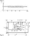
- the figure 1 is a circuit diagram of an example of a first embodiment of a protection circuit 1.
- the protection circuit 1 has an input connected to an AC voltage source 2, for example the ac mains network.
- the protection circuit 1 thus comprises an input having input terminals 151 and 152.
- the protection circuit 1 has an output connected to a consumer or electrical load 52.
- the protection circuit 1 thus comprises an output comprising output terminals. 161 and 162.
- the protection circuit 1 may for example be integrated into a household power outlet, the output terminals 161 and 162 being for example output terminals for the connection of household appliances, and the input terminals 151 and 152 being for example terminals for connection to an electrical panel via copper wires.
- the protection circuit 1 comprises a current sensor 101 connected between the input terminal 152 and the output terminal 162.
- the current sensor 101 is for example implemented in the form of a resistor in the illustrated embodiment. .
- the current sensor 101 may also be implemented in a non-limiting manner in the form of a galvanic probe or in the form of a Hall effect probe.
- the protection circuit 1 also comprises a transistor 111 and a transistor 112 connected in series with the current sensor 101 between the input terminal 152 and the output terminal 162.
- the transistors 111 and 112 are of the field effect type. high electron mobility, normally closed (or normally passing type, designated N-On). These transistors can be replaced by a single transistor of bidirectional type such as that described in the patent document US20140145203 .
- the drain of the transistor 111 is connected to the resistor 101.
- the source of the transistor 111 is connected to the source of the transistor 112 via a connection node 113.
- the drain of the transistor 112 is connected to the output terminal 162 .
- the protection circuit 1 includes a transformer 140.
- a primary winding 141 of the transformer 140 is connected across the resistor 101.
- the transformer 140 also has a secondary winding 142.
- the protection circuit 1 also comprises a rectifier bridge 130.
- the rectifier bridge 130 comprises input terminals 135 and 136.
- the winding secondary 142 is connected between these input terminals 135 and 136.
- the rectifier bridge 130 further includes output terminals 131 and 132, between which an electrical load is connected.
- the electrical load connected between the output terminals 131 and 132 is here a circuit combining a resistor 102 and a capacitor 121 connected in parallel.
- the rectifier bridge 130 comprises, in a manner known per se, four rectifying diodes 133, connected so as to form a bridge of full-wave rectifier diodes 130.
- the gate of the transistors 111 and 112 is connected to the output terminal 131 of the rectifier bridge 130.
- the intermediate node 113 is connected to the output terminal 132 of the rectifier bridge 130.
- the connection node 113 thus applies a reference potential on the output terminal 132. From this potential, a potential is applied by the output terminal 131 on the gate of the transistors 111 and 112.
- the transistors 111 and 112 of normally closed type are conductive (without external action on the gate) and have an extremely low passage resistance, due to the use of transistors 111 and 112 with high electronic mobility. Thus, the losses in the protection circuit 1 in the absence of failure are extremely small.
- the transistors 111 and 112 form a bidirectional connection current and voltage to supply the consumer 52 in AC.
- the resistor 101 advantageously has a resistance value at most equal to 2 ⁇ , and preferably equal to 0.5 ⁇ .
- the combination of the resistor 101, the transformer 140, the rectifier bridge 130, and the electrical load form a control of the transistors 111 and 112, in order to achieve a current limitation.
- a resistor 51 is here representative of the connection resistance or the line resistance to the electrical consumer 52.
- the line 53 symbolizes a short circuit bypassing the electrical consumer 52 during a failure.
- the current flowing through the transistors 111 and 112 thus ensures both their control and their own protection by current limitation.
- the gate control of the transistors 111 and 112 is isolated via the transformer 140, which guarantees its protection. Moreover, this potential is well referenced with respect to the potential of the connection node 113, independently of the current flowing through the transistors 111 and 112.
- the current limitation makes it possible to protect both the current consumer 52 and the voltage source 2, so as to be able to ensure continuity of service, instead of cutting the current between the terminals 152 and 162.
- the protection circuit 1 can guarantee a normal resumption of operation, the current limitation being interrupted as soon as the overcurrent through the protection circuit 1 disappears.
- the failure remains still detectable, so that a protective device disposed for example in an electrical panel can take a corrective action against the failure.
- the protection circuit 1 makes it possible to provide a current limitation for the two alternations of the alternating current.
- capacitor 121 makes it possible to record the short-circuit current value, in order to favor its detection in certain applications.
- the capacitor 121 may, for example, have a capacitance of 10 ⁇ F, in the form of a surface-mounted component remaining relatively easy to include in the integrated circuit 1.
- the transformer 140 will advantageously have a voltage transformation ratio of between 0.5 and 1.
- the threshold voltage of transistors 111 and 112 advantageously has an amplitude at most equal to 2V.
- the threshold voltage of transistors 111 and 112 advantageously has an amplitude at most equal to 2V.
- Normal operation at rated current is observed between 0 and 100 msec. Between times 100 and 200 ms, a short-circuit is created between the output terminals 161 and 162.
- transistors 111 and 112 having here a threshold voltage of -1.8 V, the amplitude of the current through the transistors 111 and 112 in case of failure remains close to the nominal current, here of the order of 110%.
- the simulations were carried out with a resistor 101 with a value of 0.5 ⁇ , a resistor 51 with a value of 1 m ⁇ , a resistor 52 with a value of 10 ⁇ , a sinusoidal voltage source 2 of 50 V with 50 Hz.
- the potential difference across the resistor 101 is then 5 V.
- a nominal current operation is also observed between times 0 and 100 ms. Between times 100 ms and 500 ms, a short circuit is created between the output terminals 161 and 162.
- the transistors 111 and 112 have a threshold voltage of -2.8V.
- the amplitude of the current through the transistors 111 and 112 in case of failure is a little higher than in the example of the figure 4 , of the order of 170% of the nominal current.
- the output voltage is here also illustrated in broken lines.
- connection node 113 may be formed in a layer of continuous electron gas between the transistors 111 and 112.
- Transistors 111 and 112 may have a heterojunction formed from a combination of layers of III-N material, including for example GaN. Lateral GaN transistors are well suited for symmetrical realization of transistors 111 and 112 sharing a source connected to connection node 113.
- the diodes 133 are each constituted by a normally open type high electron mobility field effect transistor whose source and gate are connected.
- Such a configuration makes it possible to make transistors 111 and 112 cointegrated with the rectifier bridge 130 on the same substrate, in order to benefit from an optimized size and cost of manufacture. Furthermore, in such a configuration, the current limiting protection occurs very rapidly, the current through the transistors 111 and 112 ensuring their own control through other cointegrated components.
- the resistor 102 consists of a high-mobility electronic field effect transistor of normally open type with negative threshold voltage, the source and the gate of which are connected. Such a configuration makes it possible to make transistors 111 and 112 cointegrated with resistor 102 on the same substrate, in order to benefit from an optimized bulk and cost of manufacture.
- transformer 140 In order to promote the integration of the transformer 140 in the integrated circuit 1, it is preferably superimposed planar type.
- the figure 4 is a circuit diagram of an example of a second embodiment of a protection circuit 1.
- This second embodiment aims in particular to facilitate the integration of the protection circuit 1.
- the protection circuit 1 is different from that of the first embodiment by the structure of the electrical load connected between the output terminals 131 and 132 of the rectifier bridge 130.
- This electrical load here consists of a resistor 102.
- the resistor 102 is IEC 60050 - International Electrotechnical Vocabulary - Details for IEV number 845-02-21 Electromagnetic field effect transistor with normally open type of negative threshold voltage, whose source and gate are connected.
- the threshold voltage of transistors 111 and 112 advantageously has an amplitude at most equal to 2V.
- Normal operation at nominal current is observed between 0 and 500 ms. Between times 500 and 1000 ms, a short-circuit is created between the output terminals 161 and 162.
- transistors 111 and 112 having here a threshold voltage of -1.8 V, the amplitude of the current through the transistors 111 and 112 in case of failure remains close to the nominal current, here of the order of 110%. A very long time is here also left to other safety devices to provide a solution to the malfunction.
- the simulations were carried out with a resistor 101 with a value of 0.5 ⁇ , a resistor 51 with a value of 1 m ⁇ , a resistor 52 with a value of 10 ⁇ , a sinusoidal voltage source 2 of 50 V with 50 Hz.
- a current of 10 A the potential difference across the resistor 101 is then 5 V.
- a transformer 140 having a transformation ratio of 1 the same potential difference of 5 V is applied between the terminals. 135 and 136.
- the figure 6 schematically illustrates the integration of a protection circuit 1 according to the first embodiment, with an AC voltage source 2 connected between its input terminals 151 and 152.
- the protection circuit 1 has a connected output interface to an electrical consumer 52.
- An electrode 31 forms a drain of the transistor 111 and is connected to the current sensor 101.
- An electrode 32 forms a drain of the transistor 112 and is connected to the output terminal 162.
- a layer of electron gas 41 is connected by two ends. to the electrode 31 and to the electrode 32 and extends continuously between these electrodes 31 and 32.
- Grid electrodes 33 and 34 are formed in line with the layer of electron gas 41 between the electrodes 31 and 32.
- a connection node between the heterojunction transistors is intrinsically formed in the electron gas layer 41 between the gate electrodes 33 and 34.
- the gate electrodes are connected to the output terminal 31.
- An electrode 35 forms a common source of two diode connected heterojunction transistors.
- the electrode 35 is connected to the output terminal 131.
- An electrode 36 forms a common drain of two other heterojunction transistors connected in a diode.
- the electrode 36 is connected to the output terminal 132.
- a four-diode rectifier bridge is formed here, each of these diodes being constituted by a respective heterojunction transistor.
- a common electrode 61 forms an electrode common to two of the heterojunction transistors, thus forming the drain of one, and the source of the other.
- the electrode 61 is positioned between the electrodes 35 and 36.
- Another common electrode 62 forms an electrode common to two of the heterojunction transistors, thus forming the drain of one and the source of the other.
- the electrode 62 is positioned between the electrodes 35 and 36.
- An electron gas layer 42 is connected by two ends to the electrode 35 and to the electrode 61 and extends continuously between these electrodes 35 and 61.
- a layer of electron gas 43 is connected by two ends. to the electrode 61 and to the electrode 36 and extends continuously between these electrodes 61 and 36.
- An electron gas layer 44 is connected by two ends to the electrode 62 and the electrode 36 and extends continuously between these electrodes 62 and 36.
- An electron gas layer 45 is connected by two ends to the electrode 35 and the electrode 62 and extends continuously between these electrodes 35 and 62.
- a gate electrode 37 is formed plumb with the layer of electron gas 42 between the electrodes 35 and 61.
- the gate electrode 37 is also formed in line with the layer of electron gas 45 between the electrodes 35 and 62.
- a gate electrode 39 is formed plumb with the layer of electron gas 43 between the electrodes 61 and 36.
- a gate electrode 38 is formed in line with the layer of electron gas 44 between the electrodes 62 and 36.
- the gate electrodes 37 and 39 are connected to a first terminal of the secondary winding 142, the gate electrode 38 is connected to a second terminal of the secondary winding 142.
- the electron gas layers 41 to 45 are shown in dotted lines to illustrate that they can be formed from the same substrate and be isolated from each other by photolithography steps.
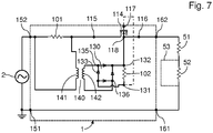
- the figure 7 is a circuit diagram of an example of a third embodiment of a protection circuit 1.
- This third embodiment aims to replace transistors 111 and 112 of the first and second embodiments by a bidirectional transistor 114, such as the one described in the document EP2736078 .
- the third embodiment is here presented as a variation of the second embodiment, but the bidirectional transistor presented here can also be used to replace the transistors 111 and 112 of the first embodiment.
- the protection circuit 1 has an input connected to an AC voltage source 2 and thus comprises an input having input terminals 151 and 152.
- the protection circuit 1 has an output connected to a consumer or electric load 52 and thus comprises an output having output terminals 161 and 162.
- the protection circuit 1 comprises a current sensor 101 connected between the input terminal 152 and the output terminal 162, as detailed in the previous embodiments.
- the protection circuit 1 also comprises a bidirectional transistor 114.
- the transistor 114 is of the electronically-exchangeable field effect type, of normally closed type.
- the transistor 114 includes in a manner known per se a layer of electron gas.
- the drain 115 of the transistor 114 is connected to the resistor 101.
- the source 116 of the transistor 114 is connected to the output terminal 162.
- the transistor 114 furthermore comprises a reference electrode 118 in line with its gas layer. electrons, between the electrodes 115 and 116.
- the reference electrode 118 is at the potential of the layer of the layer of electron gas located vertically.
- the electrode 118 is formed in a semiconductor layer of the transistor 114, and electrically connected to the layer of electron gas located vertically, either by direct connection or by tunnel connection.
- the protection circuit 1 comprises a transformer 140 whose primary winding 141 is connected across the terminals of the resistor 101.
- the transformer 140 also has a secondary winding 142.
- the protection circuit 1 also comprises a rectifier bridge 130 with input terminals 135 and 136 between which the secondary winding 142 is connected.
- the rectifier bridge 130 furthermore has output terminals 131 and 132, between which a resistor 102 is connected.
- the resistor 102 may consist of a normally open-type negative-threshold electronic high-mobility field effect transistor whose source and gate are connected.
- the rectifier bridge 130 has four rectifying diodes 133, connected to form a bridge of rectifying diodes 130 full wave.
- the gate 117 of the transistor 114 is connected to the output terminal 131 of the rectifier bridge 130.
- the reference electrode 118 is connected to the output terminal 132 of the rectifier bridge 130. The reference electrode 118 thus applies a reference potential on the output terminal 132. From this potential, a potential is applied by the output terminal 131 on the gate 117 of the transistor 114.
- the transistor 114 of the normally closed type is conductive (without external action on the gate 117) and has an extremely reduced through resistance, due to the use of a transistor 114 with high electronic mobility. Thus, the losses in the protection circuit 1 in the absence of failure are extremely small.
Landscapes
- Engineering & Computer Science (AREA)
- Power Engineering (AREA)
- Physics & Mathematics (AREA)
- General Physics & Mathematics (AREA)
- Electromagnetism (AREA)
- Radar, Positioning & Navigation (AREA)
- Automation & Control Theory (AREA)
- Junction Field-Effect Transistors (AREA)
- Semiconductor Integrated Circuits (AREA)
Claims (15)
- Schutzschaltung (1) eines elektrischen Verbrauchers, welche aufweist:- eine Eingangsschnittstelle, welche eine erste und eine zweite Eingangsklemme (151, 152) zum Anlegen einer Wechselpotentialdifferenz aufweist;- eine Ausgangsschnittstelle, welche eine erste und eine zweite Ausgangsklemme (161, 162) zum Anschluss eines elektrischen Verbrauchers aufweist;- einen Stromsensor (101), der zwischen die zweite Eingangsklemme und die zweite Ausgangsklemme (152, 162) geschaltet ist;- einen ersten und einen zweiten Feldeffekttransistor, wobei der erste und der zweite Transistor über einen Verbindungsknoten (113) in Reihe geschaltet sind;- eine Gleichrichterbrücke (130), die zwei Eingangsklemmen (135, 136) aufweist und eine erste und eine zweite Ausgangsklemme (131, 132) aufweist, zwischen welche eine elektrische Last (102) geschaltet ist;dadurch gekennzeichnet, dass:- der erste und der zweite Feldeffekttransistor Transistoren mit hoher elektronischer Mobilität vom normalerweise geschlossenen Typ (111, 112) sind, die mit dem Stromsensor zwischen der zweiten Eingangsklemme und der zweiten Ausgangsklemme (152, 162) in Reihe geschaltet sind;- die Schutzschaltung außerdem einen Transformator (140) umfasst, von dem eine Primärwicklung (141) mit den Klemmen des Stromsensors (101) verbunden ist und der eine Sekundärwicklung (142) umfasst;- die Eingangsklemmen der Gleichrichterbrücke (130) mit den Klemmen der Sekundärwicklung (142) verbunden sind, wobei die erste Ausgangsklemme (131) der Gleichrichterbrücke (130) mit einem Steuergate des ersten Transistors und einem Steuergate des zweiten Transistors verbunden ist, wobei die zweite Ausgangsklemme (132) der Gleichrichterbrücke mit dem Verbindungsknoten (113) verbunden ist.
- Schutzschaltung (1) eines elektrischen Verbrauchers nach Anspruch 1, wobei der erste und der zweite Transistor (111, 112) jeweils eine Schwellenspannung mit einer Amplitude aufweisen, die höchstens gleich 2 V ist.
- Schutzschaltung (1) eines elektrischen Verbrauchers nach Anspruch 1 oder 2, wobei die Gleichrichterbrücke (130) eine Diodenbrücke enthält.
- Schutzschaltung (1) eines elektrischen Verbrauchers nach Anspruch 3, wobei jede Diode der Diodenbrücke aus einem Feldeffekttransistor mit hoher elektronischer Mobilität vom normalerweise offenen Typ besteht, dessen Source und Gate verbunden sind.
- Schutzschaltung (1) eines elektrischen Verbrauchers nach Anspruch 4, wobei der erste und der zweite Transistor und die Transistoren der Diodenbrücke zusammen auf demselben Substrat integriert sind.
- Schutzschaltung (1) eines elektrischen Verbrauchers nach einem der vorhergehenden Ansprüche, wobei der Stromsensor (101) ein Widerstand ist, an dessen Klemmen die Primärwicklung (141) des Transformators (140) angeschlossen ist.
- Schutzschaltung (1) eines elektrischen Verbrauchers nach Anspruch 6, wobei der Widerstand (101) einen Widerstandswert von höchstens 2 Ω aufweist.
- Schutzschaltung (1) eines elektrischen Verbrauchers nach einem der vorhergehenden Ansprüche, wobei die elektrische Last, die zwischen die erste und die zweite Ausgangsklemme (131, 132) der Gleichrichterbrücke (130) geschaltet ist, aus einem Widerstand (102) besteht.
- Schutzschaltung (1) eines elektrischen Verbrauchers nach einem der Ansprüche 1 bis 7, wobei die elektrische Last, die zwischen die erste und die zweite Ausgangsklemme (131, 132) der Gleichrichterbrücke (130) geschaltet ist, einen Widerstand (102) umfasst, der zu einem Kondensator (121) parallelgeschaltet ist.
- Schutzschaltung (1) eines elektrischen Verbrauchers nach Anspruch 8 oder 9, wobei der Widerstand (102) aus einem Feldeffekttransistor mit hoher elektronischer Mobilität vom normalerweise offenen Typ mit negativer Schwellenspannung besteht, dessen Source und Gate verbunden sind.
- Schutzschaltung (1) eines elektrischen Verbrauchers nach einem der vorhergehenden Ansprüche, wobei das Spannungstransformationsverhältnis zwischen der Primärwicklung und der Sekundärwicklung des Transformators zwischen 0,5 und 1 liegt.
- Schutzschaltung (1) eines elektrischen Verbrauchers nach einem der vorhergehenden Ansprüche, wobei der erste und der zweite Transistor (11, 112) einen Heteroübergang aufweisen, der aus einer GaN-Schicht gebildet ist.
- Schutzschaltung (1) eines elektrischen Verbrauchers, welche aufweist:- eine Eingangsschnittstelle, welche eine erste und eine zweite Eingangsklemme (151, 152) zum Anlegen einer Wechselpotentialdifferenz aufweist;- eine Ausgangsschnittstelle, welche eine erste und eine zweite Ausgangsklemme (161, 162) zum Anschluss eines elektrischen Verbrauchers aufweist;- einen Stromsensor (101), der zwischen die zweite Eingangsklemme und die zweite Ausgangsklemme (152, 162) geschaltet ist;- einen bidirektionalen Feldeffekttransistor (114), wobei dieser Transistor über eine erste und eine zweite Leitungselektrode (115, 116) zwischen der zweiten Eingangsklemme und der zweiten Ausgangsklemme (152, 162) in Reihe geschaltet ist, wobei der Stromsensor (101) den Strom misst, der durch den bidirektionalen Transistor fließt;- eine Gleichrichterbrücke (130), die zwei Eingangsklemmen (135, 136) aufweist und eine erste und eine zweite Ausgangsklemme (131, 132) aufweist, zwischen welche eine elektrische Last (102) geschaltet ist,dadurch gekennzeichnet, dass:- der bidirektionale Transistor ein Transistor mit hoher elektronischer Mobilität vom normalerweise geschlossenen Typ ist, der eine Elektronengasschicht aufweist, wobei der bidirektionale Transistor eine Referenzelektrode (118) aufweist, die auf einer senkrechten Linie mit der Elektronengasschicht in einer Zwischenposition zwischen der ersten und der zweiten Leitungselektrode angeordnet ist, und wobei die Referenzelektrode auf dem Potential der Elektronengasschicht liegt, die auf einer senkrechten Linie mit ihr angeordnet ist;- die Schutzschaltung außerdem einen Transformator (140) umfasst, von dem eine Primärwicklung (141) mit den Klemmen des Stromsensors (101) verbunden ist und der eine Sekundärwicklung (142) umfasst;- die Eingangsklemmen der Gleichrichterbrücke (130) mit den Klemmen der Sekundärwicklung (142) verbunden sind, wobei die erste Ausgangsklemme (131) der Gleichrichterbrücke (130) mit einem Steuergate (117) des bidirektionalen Transistors verbunden ist, wobei die zweite Ausgangsklemme (132) der Gleichrichterbrücke mit der Referenzelektrode (118) verbunden ist.
- Schutzschaltung (1) eines elektrischen Verbrauchers nach Anspruch 13, wobei jede Diode der Diodenbrücke aus einem Feldeffekttransistor mit hoher elektronischer Mobilität vom normalerweise offenen Typ besteht, dessen Source und Gate verbunden sind.
- Schutzschaltung (1) eines elektrischen Verbrauchers nach Anspruch 14, wobei der der bidirektionale Transistor (114) und die Transistoren der Diodenbrücke zusammen auf demselben Substrat integriert sind.
Applications Claiming Priority (1)
| Application Number | Priority Date | Filing Date | Title |
|---|---|---|---|
| FR1658825A FR3056346B1 (fr) | 2016-09-20 | 2016-09-20 | Limiteur de courant pour charge courant alternatif |
Publications (2)
| Publication Number | Publication Date |
|---|---|
| EP3297112A1 EP3297112A1 (de) | 2018-03-21 |
| EP3297112B1 true EP3297112B1 (de) | 2019-01-30 |
Family
ID=57583239
Family Applications (1)
| Application Number | Title | Priority Date | Filing Date |
|---|---|---|---|
| EP17190733.0A Active EP3297112B1 (de) | 2016-09-20 | 2017-09-12 | Strombegrenzer für wechselstromlast |
Country Status (3)
| Country | Link |
|---|---|
| US (1) | US10474172B2 (de) |
| EP (1) | EP3297112B1 (de) |
| FR (1) | FR3056346B1 (de) |
Family Cites Families (9)
| Publication number | Priority date | Publication date | Assignee | Title |
|---|---|---|---|---|
| US3707708A (en) * | 1970-12-16 | 1972-12-26 | Multra Guard Inc | Muting circuit for a security alarm system providing a sonic alert |
| US5684663A (en) | 1995-09-29 | 1997-11-04 | Motorola, Inc. | Protection element and method for protecting a circuit |
| FR2767017B1 (fr) * | 1997-07-31 | 1999-10-15 | Sgs Thomson Microelectronics | Circuit limiteur de courant d'appel |
| US7355867B2 (en) * | 2004-08-17 | 2008-04-08 | Elster Electricity, Llc | Power supply for an electric meter having a high-voltage regulator that limits the voltage applied to certain components below the normal operating input voltage |
| WO2011156768A2 (en) * | 2010-06-11 | 2011-12-15 | Mojo Mobility, Inc. | System for wireless power transfer that supports interoperability, and multi-pole magnets for use therewith |
| US9778666B2 (en) * | 2012-04-27 | 2017-10-03 | Keithley Instruments, Llc | Dynamic current limit apparatus and method |
| WO2014052810A1 (en) * | 2012-09-28 | 2014-04-03 | Arc Suppression Technologies | Arc suppressor, system, and method |
| FR3024010A1 (fr) * | 2014-07-17 | 2016-01-22 | Commissariat Energie Atomique | Dispositif incluant une diode electroluminescente et un transformateur associe |
| FR3028666A1 (fr) * | 2014-11-17 | 2016-05-20 | Commissariat Energie Atomique | Circuit integre a structure de commutation de puissance |
-
2016
- 2016-09-20 FR FR1658825A patent/FR3056346B1/fr not_active Expired - Fee Related
-
2017
- 2017-09-12 EP EP17190733.0A patent/EP3297112B1/de active Active
- 2017-09-20 US US15/710,277 patent/US10474172B2/en active Active
Non-Patent Citations (1)
| Title |
|---|
| None * |
Also Published As
| Publication number | Publication date |
|---|---|
| EP3297112A1 (de) | 2018-03-21 |
| FR3056346A1 (fr) | 2018-03-23 |
| FR3056346B1 (fr) | 2018-10-19 |
| US20180081381A1 (en) | 2018-03-22 |
| US10474172B2 (en) | 2019-11-12 |
Similar Documents
| Publication | Publication Date | Title |
|---|---|---|
| FR3035751A1 (fr) | Coupe-circuit pour courant continu et procede d'utilisation | |
| FR2955986A1 (fr) | Dispositif de deviation de surcharges de courant ou de surtensions transitoires | |
| EP1950885A1 (de) | Steuervorrichtung eines elektronischen Leistungstrenners und eine solche Vorrichtung umfassender Stromrichter | |
| FR3012696A1 (fr) | Circuit de protection contre des surtensions | |
| EP2822126B1 (de) | Differenzialschutzvorrichtung für ein Unterbrechungsgerät, und eine solche Vorrichtung umfassendes elektrisches Unterbrechungsgerät | |
| FR2873509A1 (fr) | Dispositif de protection contre les surtensions a capacite de coupure du courant de fuite ameliore | |
| EP0677907B1 (de) | Überstromschutzvorrichtung | |
| EP3297112B1 (de) | Strombegrenzer für wechselstromlast | |
| FR2635929A1 (fr) | Dispositif a semi-conducteur possedant un circuit de protection contre les courts-circuits | |
| FR3021167B1 (fr) | Circuit de derivation d'energie et procede de mise en fonctionnement de ce circuit | |
| CA3087843A1 (fr) | Dispositif de protection d'un equipement electrique | |
| EP0619637B1 (de) | Schutz eines Kraftfahrzeugdrehstromgenerators | |
| FR2964263A1 (fr) | Circuit de reduction d'intensite de fuite de courant alternatif | |
| WO2020164945A1 (fr) | Systeme de commutation statique et de limitation d'un courant continu | |
| EP1111750B1 (de) | Schutzvorrichtung gegen elektrische Fehler | |
| EP3437115B1 (de) | Hybridisierungsystem für hochspannungsgleichstrom | |
| FR2975542A1 (fr) | Systeme d'alimentation electrique en courant et tension continus protege par un limiteur en courant et son procede de protection | |
| EP0895331A1 (de) | Schutzvorrichtung für elektrische Last und Versorgungseinrichtung mit einer solchen Vorrichtung | |
| CA2855783A1 (fr) | Dispositif et procede de protection contre des courants de fuite | |
| FR3016751A1 (fr) | Dispositif de protection d'un circuit contre des surtensions et organe d'alimentation electrique comprenant un tel dispositif | |
| EP2198507B1 (de) | Variable steuerung | |
| FR2975530A1 (fr) | Composant electronique d'un limiteur de courant pour proteger une alimentation electrique | |
| EP4376039A1 (de) | Abschaltvorrichtung für elektrische schaltung mit überspannungsschutz und abschaltverfahren dafür | |
| JP2020030969A (ja) | 過電圧抑制回路及び遮断装置 | |
| FR3089360A1 (fr) | Variateur électronique pour circuit basse tension |
Legal Events
| Date | Code | Title | Description |
|---|---|---|---|
| PUAI | Public reference made under article 153(3) epc to a published international application that has entered the european phase |
Free format text: ORIGINAL CODE: 0009012 |
|
| STAA | Information on the status of an ep patent application or granted ep patent |
Free format text: STATUS: REQUEST FOR EXAMINATION WAS MADE |
|
| 17P | Request for examination filed |
Effective date: 20170912 |
|
| AK | Designated contracting states |
Kind code of ref document: A1 Designated state(s): AL AT BE BG CH CY CZ DE DK EE ES FI FR GB GR HR HU IE IS IT LI LT LU LV MC MK MT NL NO PL PT RO RS SE SI SK SM TR |
|
| AX | Request for extension of the european patent |
Extension state: BA ME |
|
| GRAP | Despatch of communication of intention to grant a patent |
Free format text: ORIGINAL CODE: EPIDOSNIGR1 |
|
| STAA | Information on the status of an ep patent application or granted ep patent |
Free format text: STATUS: GRANT OF PATENT IS INTENDED |
|
| RIC1 | Information provided on ipc code assigned before grant |
Ipc: G01R 1/36 20060101ALI20180727BHEP Ipc: H02H 9/02 20060101AFI20180727BHEP Ipc: G05F 1/56 20060101ALI20180727BHEP |
|
| INTG | Intention to grant announced |
Effective date: 20180820 |
|
| GRAS | Grant fee paid |
Free format text: ORIGINAL CODE: EPIDOSNIGR3 |
|
| GRAA | (expected) grant |
Free format text: ORIGINAL CODE: 0009210 |
|
| STAA | Information on the status of an ep patent application or granted ep patent |
Free format text: STATUS: THE PATENT HAS BEEN GRANTED |
|
| AK | Designated contracting states |
Kind code of ref document: B1 Designated state(s): AL AT BE BG CH CY CZ DE DK EE ES FI FR GB GR HR HU IE IS IT LI LT LU LV MC MK MT NL NO PL PT RO RS SE SI SK SM TR |
|
| REG | Reference to a national code |
Ref country code: GB Ref legal event code: FG4D Free format text: NOT ENGLISH |
|
| REG | Reference to a national code |
Ref country code: CH Ref legal event code: EP |
|
| REG | Reference to a national code |
Ref country code: AT Ref legal event code: REF Ref document number: 1094013 Country of ref document: AT Kind code of ref document: T Effective date: 20190215 |
|
| REG | Reference to a national code |
Ref country code: IE Ref legal event code: FG4D Free format text: LANGUAGE OF EP DOCUMENT: FRENCH |
|
| REG | Reference to a national code |
Ref country code: DE Ref legal event code: R096 Ref document number: 602017002011 Country of ref document: DE |
|
| REG | Reference to a national code |
Ref country code: NL Ref legal event code: MP Effective date: 20190130 |
|
| REG | Reference to a national code |
Ref country code: LT Ref legal event code: MG4D |
|
| PG25 | Lapsed in a contracting state [announced via postgrant information from national office to epo] |
Ref country code: SE Free format text: LAPSE BECAUSE OF FAILURE TO SUBMIT A TRANSLATION OF THE DESCRIPTION OR TO PAY THE FEE WITHIN THE PRESCRIBED TIME-LIMIT Effective date: 20190130 Ref country code: NL Free format text: LAPSE BECAUSE OF FAILURE TO SUBMIT A TRANSLATION OF THE DESCRIPTION OR TO PAY THE FEE WITHIN THE PRESCRIBED TIME-LIMIT Effective date: 20190130 Ref country code: FI Free format text: LAPSE BECAUSE OF FAILURE TO SUBMIT A TRANSLATION OF THE DESCRIPTION OR TO PAY THE FEE WITHIN THE PRESCRIBED TIME-LIMIT Effective date: 20190130 Ref country code: ES Free format text: LAPSE BECAUSE OF FAILURE TO SUBMIT A TRANSLATION OF THE DESCRIPTION OR TO PAY THE FEE WITHIN THE PRESCRIBED TIME-LIMIT Effective date: 20190130 Ref country code: LT Free format text: LAPSE BECAUSE OF FAILURE TO SUBMIT A TRANSLATION OF THE DESCRIPTION OR TO PAY THE FEE WITHIN THE PRESCRIBED TIME-LIMIT Effective date: 20190130 Ref country code: PL Free format text: LAPSE BECAUSE OF FAILURE TO SUBMIT A TRANSLATION OF THE DESCRIPTION OR TO PAY THE FEE WITHIN THE PRESCRIBED TIME-LIMIT Effective date: 20190130 Ref country code: PT Free format text: LAPSE BECAUSE OF FAILURE TO SUBMIT A TRANSLATION OF THE DESCRIPTION OR TO PAY THE FEE WITHIN THE PRESCRIBED TIME-LIMIT Effective date: 20190530 Ref country code: NO Free format text: LAPSE BECAUSE OF FAILURE TO SUBMIT A TRANSLATION OF THE DESCRIPTION OR TO PAY THE FEE WITHIN THE PRESCRIBED TIME-LIMIT Effective date: 20190430 |
|
| REG | Reference to a national code |
Ref country code: AT Ref legal event code: MK05 Ref document number: 1094013 Country of ref document: AT Kind code of ref document: T Effective date: 20190130 |
|
| PG25 | Lapsed in a contracting state [announced via postgrant information from national office to epo] |
Ref country code: LV Free format text: LAPSE BECAUSE OF FAILURE TO SUBMIT A TRANSLATION OF THE DESCRIPTION OR TO PAY THE FEE WITHIN THE PRESCRIBED TIME-LIMIT Effective date: 20190130 Ref country code: GR Free format text: LAPSE BECAUSE OF FAILURE TO SUBMIT A TRANSLATION OF THE DESCRIPTION OR TO PAY THE FEE WITHIN THE PRESCRIBED TIME-LIMIT Effective date: 20190501 Ref country code: RS Free format text: LAPSE BECAUSE OF FAILURE TO SUBMIT A TRANSLATION OF THE DESCRIPTION OR TO PAY THE FEE WITHIN THE PRESCRIBED TIME-LIMIT Effective date: 20190130 Ref country code: IS Free format text: LAPSE BECAUSE OF FAILURE TO SUBMIT A TRANSLATION OF THE DESCRIPTION OR TO PAY THE FEE WITHIN THE PRESCRIBED TIME-LIMIT Effective date: 20190530 Ref country code: BG Free format text: LAPSE BECAUSE OF FAILURE TO SUBMIT A TRANSLATION OF THE DESCRIPTION OR TO PAY THE FEE WITHIN THE PRESCRIBED TIME-LIMIT Effective date: 20190430 Ref country code: HR Free format text: LAPSE BECAUSE OF FAILURE TO SUBMIT A TRANSLATION OF THE DESCRIPTION OR TO PAY THE FEE WITHIN THE PRESCRIBED TIME-LIMIT Effective date: 20190130 |
|
| PG25 | Lapsed in a contracting state [announced via postgrant information from national office to epo] |
Ref country code: DK Free format text: LAPSE BECAUSE OF FAILURE TO SUBMIT A TRANSLATION OF THE DESCRIPTION OR TO PAY THE FEE WITHIN THE PRESCRIBED TIME-LIMIT Effective date: 20190130 Ref country code: EE Free format text: LAPSE BECAUSE OF FAILURE TO SUBMIT A TRANSLATION OF THE DESCRIPTION OR TO PAY THE FEE WITHIN THE PRESCRIBED TIME-LIMIT Effective date: 20190130 Ref country code: AL Free format text: LAPSE BECAUSE OF FAILURE TO SUBMIT A TRANSLATION OF THE DESCRIPTION OR TO PAY THE FEE WITHIN THE PRESCRIBED TIME-LIMIT Effective date: 20190130 Ref country code: SK Free format text: LAPSE BECAUSE OF FAILURE TO SUBMIT A TRANSLATION OF THE DESCRIPTION OR TO PAY THE FEE WITHIN THE PRESCRIBED TIME-LIMIT Effective date: 20190130 Ref country code: CZ Free format text: LAPSE BECAUSE OF FAILURE TO SUBMIT A TRANSLATION OF THE DESCRIPTION OR TO PAY THE FEE WITHIN THE PRESCRIBED TIME-LIMIT Effective date: 20190130 Ref country code: RO Free format text: LAPSE BECAUSE OF FAILURE TO SUBMIT A TRANSLATION OF THE DESCRIPTION OR TO PAY THE FEE WITHIN THE PRESCRIBED TIME-LIMIT Effective date: 20190130 |
|
| REG | Reference to a national code |
Ref country code: DE Ref legal event code: R097 Ref document number: 602017002011 Country of ref document: DE |
|
| PG25 | Lapsed in a contracting state [announced via postgrant information from national office to epo] |
Ref country code: SM Free format text: LAPSE BECAUSE OF FAILURE TO SUBMIT A TRANSLATION OF THE DESCRIPTION OR TO PAY THE FEE WITHIN THE PRESCRIBED TIME-LIMIT Effective date: 20190130 |
|
| PLBE | No opposition filed within time limit |
Free format text: ORIGINAL CODE: 0009261 |
|
| STAA | Information on the status of an ep patent application or granted ep patent |
Free format text: STATUS: NO OPPOSITION FILED WITHIN TIME LIMIT |
|
| PG25 | Lapsed in a contracting state [announced via postgrant information from national office to epo] |
Ref country code: AT Free format text: LAPSE BECAUSE OF FAILURE TO SUBMIT A TRANSLATION OF THE DESCRIPTION OR TO PAY THE FEE WITHIN THE PRESCRIBED TIME-LIMIT Effective date: 20190130 |
|
| 26N | No opposition filed |
Effective date: 20191031 |
|
| PG25 | Lapsed in a contracting state [announced via postgrant information from national office to epo] |
Ref country code: SI Free format text: LAPSE BECAUSE OF FAILURE TO SUBMIT A TRANSLATION OF THE DESCRIPTION OR TO PAY THE FEE WITHIN THE PRESCRIBED TIME-LIMIT Effective date: 20190130 |
|
| PG25 | Lapsed in a contracting state [announced via postgrant information from national office to epo] |
Ref country code: TR Free format text: LAPSE BECAUSE OF FAILURE TO SUBMIT A TRANSLATION OF THE DESCRIPTION OR TO PAY THE FEE WITHIN THE PRESCRIBED TIME-LIMIT Effective date: 20190130 |
|
| PG25 | Lapsed in a contracting state [announced via postgrant information from national office to epo] |
Ref country code: MC Free format text: LAPSE BECAUSE OF FAILURE TO SUBMIT A TRANSLATION OF THE DESCRIPTION OR TO PAY THE FEE WITHIN THE PRESCRIBED TIME-LIMIT Effective date: 20190130 |
|
| PG25 | Lapsed in a contracting state [announced via postgrant information from national office to epo] |
Ref country code: LU Free format text: LAPSE BECAUSE OF NON-PAYMENT OF DUE FEES Effective date: 20190912 Ref country code: IE Free format text: LAPSE BECAUSE OF NON-PAYMENT OF DUE FEES Effective date: 20190912 |
|
| REG | Reference to a national code |
Ref country code: BE Ref legal event code: MM Effective date: 20190930 |
|
| PG25 | Lapsed in a contracting state [announced via postgrant information from national office to epo] |
Ref country code: BE Free format text: LAPSE BECAUSE OF NON-PAYMENT OF DUE FEES Effective date: 20190930 |
|
| REG | Reference to a national code |
Ref country code: CH Ref legal event code: PL |
|
| PG25 | Lapsed in a contracting state [announced via postgrant information from national office to epo] |
Ref country code: CY Free format text: LAPSE BECAUSE OF FAILURE TO SUBMIT A TRANSLATION OF THE DESCRIPTION OR TO PAY THE FEE WITHIN THE PRESCRIBED TIME-LIMIT Effective date: 20190130 |
|
| PG25 | Lapsed in a contracting state [announced via postgrant information from national office to epo] |
Ref country code: HU Free format text: LAPSE BECAUSE OF FAILURE TO SUBMIT A TRANSLATION OF THE DESCRIPTION OR TO PAY THE FEE WITHIN THE PRESCRIBED TIME-LIMIT; INVALID AB INITIO Effective date: 20170912 Ref country code: MT Free format text: LAPSE BECAUSE OF FAILURE TO SUBMIT A TRANSLATION OF THE DESCRIPTION OR TO PAY THE FEE WITHIN THE PRESCRIBED TIME-LIMIT Effective date: 20190130 |
|
| PG25 | Lapsed in a contracting state [announced via postgrant information from national office to epo] |
Ref country code: CH Free format text: LAPSE BECAUSE OF NON-PAYMENT OF DUE FEES Effective date: 20200930 Ref country code: LI Free format text: LAPSE BECAUSE OF NON-PAYMENT OF DUE FEES Effective date: 20200930 |
|
| PG25 | Lapsed in a contracting state [announced via postgrant information from national office to epo] |
Ref country code: MK Free format text: LAPSE BECAUSE OF FAILURE TO SUBMIT A TRANSLATION OF THE DESCRIPTION OR TO PAY THE FEE WITHIN THE PRESCRIBED TIME-LIMIT Effective date: 20190130 |
|
| PGFP | Annual fee paid to national office [announced via postgrant information from national office to epo] |
Ref country code: GB Payment date: 20230920 Year of fee payment: 7 |
|
| PGFP | Annual fee paid to national office [announced via postgrant information from national office to epo] |
Ref country code: FR Payment date: 20230920 Year of fee payment: 7 Ref country code: DE Payment date: 20230919 Year of fee payment: 7 |
|
| PGFP | Annual fee paid to national office [announced via postgrant information from national office to epo] |
Ref country code: IT Payment date: 20230929 Year of fee payment: 7 |