EP3291311A1 - Semiconductor detector - Google Patents
Semiconductor detector Download PDFInfo
- Publication number
- EP3291311A1 EP3291311A1 EP17188640.1A EP17188640A EP3291311A1 EP 3291311 A1 EP3291311 A1 EP 3291311A1 EP 17188640 A EP17188640 A EP 17188640A EP 3291311 A1 EP3291311 A1 EP 3291311A1
- Authority
- EP
- European Patent Office
- Prior art keywords
- detector
- semiconductor detector
- crystal
- circuit board
- field enhanced
- Prior art date
- Legal status (The legal status is an assumption and is not a legal conclusion. Google has not performed a legal analysis and makes no representation as to the accuracy of the status listed.)
- Granted
Links
Images


Classifications
-
- G—PHYSICS
- G01—MEASURING; TESTING
- G01T—MEASUREMENT OF NUCLEAR OR X-RADIATION
- G01T1/00—Measuring X-radiation, gamma radiation, corpuscular radiation, or cosmic radiation
- G01T1/16—Measuring radiation intensity
- G01T1/24—Measuring radiation intensity with semiconductor detectors
-
- G—PHYSICS
- G01—MEASURING; TESTING
- G01T—MEASUREMENT OF NUCLEAR OR X-RADIATION
- G01T1/00—Measuring X-radiation, gamma radiation, corpuscular radiation, or cosmic radiation
-
- G—PHYSICS
- G01—MEASURING; TESTING
- G01T—MEASUREMENT OF NUCLEAR OR X-RADIATION
- G01T1/00—Measuring X-radiation, gamma radiation, corpuscular radiation, or cosmic radiation
- G01T1/16—Measuring radiation intensity
- G01T1/24—Measuring radiation intensity with semiconductor detectors
- G01T1/241—Electrode arrangements, e.g. continuous or parallel strips or the like
-
- H—ELECTRICITY
- H05—ELECTRIC TECHNIQUES NOT OTHERWISE PROVIDED FOR
- H05K—PRINTED CIRCUITS; CASINGS OR CONSTRUCTIONAL DETAILS OF ELECTRIC APPARATUS; MANUFACTURE OF ASSEMBLAGES OF ELECTRICAL COMPONENTS
- H05K1/00—Printed circuits
- H05K1/02—Details
- H05K1/0213—Electrical arrangements not otherwise provided for
- H05K1/0216—Reduction of cross-talk, noise or electromagnetic interference
- H05K1/023—Reduction of cross-talk, noise or electromagnetic interference using auxiliary mounted passive components or auxiliary substances
- H05K1/0233—Filters, inductors or a magnetic substance
-
- H—ELECTRICITY
- H05—ELECTRIC TECHNIQUES NOT OTHERWISE PROVIDED FOR
- H05K—PRINTED CIRCUITS; CASINGS OR CONSTRUCTIONAL DETAILS OF ELECTRIC APPARATUS; MANUFACTURE OF ASSEMBLAGES OF ELECTRICAL COMPONENTS
- H05K1/00—Printed circuits
- H05K1/02—Details
- H05K1/0277—Bendability or stretchability details
- H05K1/028—Bending or folding regions of flexible printed circuits
-
- H—ELECTRICITY
- H05—ELECTRIC TECHNIQUES NOT OTHERWISE PROVIDED FOR
- H05K—PRINTED CIRCUITS; CASINGS OR CONSTRUCTIONAL DETAILS OF ELECTRIC APPARATUS; MANUFACTURE OF ASSEMBLAGES OF ELECTRICAL COMPONENTS
- H05K1/00—Printed circuits
- H05K1/02—Details
- H05K1/11—Printed elements for providing electric connections to or between printed circuits
- H05K1/115—Via connections; Lands around holes or via connections
-
- H—ELECTRICITY
- H05—ELECTRIC TECHNIQUES NOT OTHERWISE PROVIDED FOR
- H05K—PRINTED CIRCUITS; CASINGS OR CONSTRUCTIONAL DETAILS OF ELECTRIC APPARATUS; MANUFACTURE OF ASSEMBLAGES OF ELECTRICAL COMPONENTS
- H05K1/00—Printed circuits
- H05K1/18—Printed circuits structurally associated with non-printed electric components
- H05K1/181—Printed circuits structurally associated with non-printed electric components associated with surface mounted components
-
- H—ELECTRICITY
- H10—SEMICONDUCTOR DEVICES; ELECTRIC SOLID-STATE DEVICES NOT OTHERWISE PROVIDED FOR
- H10F—INORGANIC SEMICONDUCTOR DEVICES SENSITIVE TO INFRARED RADIATION, LIGHT, ELECTROMAGNETIC RADIATION OF SHORTER WAVELENGTH OR CORPUSCULAR RADIATION
- H10F30/00—Individual radiation-sensitive semiconductor devices in which radiation controls the flow of current through the devices, e.g. photodetectors
- H10F30/20—Individual radiation-sensitive semiconductor devices in which radiation controls the flow of current through the devices, e.g. photodetectors the devices having potential barriers, e.g. phototransistors
- H10F30/29—Individual radiation-sensitive semiconductor devices in which radiation controls the flow of current through the devices, e.g. photodetectors the devices having potential barriers, e.g. phototransistors the devices being sensitive to radiation having very short wavelengths, e.g. X-rays, gamma-rays or corpuscular radiation
-
- H—ELECTRICITY
- H10—SEMICONDUCTOR DEVICES; ELECTRIC SOLID-STATE DEVICES NOT OTHERWISE PROVIDED FOR
- H10F—INORGANIC SEMICONDUCTOR DEVICES SENSITIVE TO INFRARED RADIATION, LIGHT, ELECTROMAGNETIC RADIATION OF SHORTER WAVELENGTH OR CORPUSCULAR RADIATION
- H10F30/00—Individual radiation-sensitive semiconductor devices in which radiation controls the flow of current through the devices, e.g. photodetectors
- H10F30/20—Individual radiation-sensitive semiconductor devices in which radiation controls the flow of current through the devices, e.g. photodetectors the devices having potential barriers, e.g. phototransistors
- H10F30/29—Individual radiation-sensitive semiconductor devices in which radiation controls the flow of current through the devices, e.g. photodetectors the devices having potential barriers, e.g. phototransistors the devices being sensitive to radiation having very short wavelengths, e.g. X-rays, gamma-rays or corpuscular radiation
- H10F30/298—Individual radiation-sensitive semiconductor devices in which radiation controls the flow of current through the devices, e.g. photodetectors the devices having potential barriers, e.g. phototransistors the devices being sensitive to radiation having very short wavelengths, e.g. X-rays, gamma-rays or corpuscular radiation the devices being characterised by field-effect operation, e.g. MIS type detectors
-
- H—ELECTRICITY
- H10—SEMICONDUCTOR DEVICES; ELECTRIC SOLID-STATE DEVICES NOT OTHERWISE PROVIDED FOR
- H10F—INORGANIC SEMICONDUCTOR DEVICES SENSITIVE TO INFRARED RADIATION, LIGHT, ELECTROMAGNETIC RADIATION OF SHORTER WAVELENGTH OR CORPUSCULAR RADIATION
- H10F77/00—Constructional details of devices covered by this subclass
- H10F77/10—Semiconductor bodies
- H10F77/12—Active materials
- H10F77/123—Active materials comprising only Group II-VI materials, e.g. CdS, ZnS or HgCdTe
- H10F77/1237—Active materials comprising only Group II-VI materials, e.g. CdS, ZnS or HgCdTe having at least three elements, e.g. HgCdTe
-
- H—ELECTRICITY
- H10—SEMICONDUCTOR DEVICES; ELECTRIC SOLID-STATE DEVICES NOT OTHERWISE PROVIDED FOR
- H10F—INORGANIC SEMICONDUCTOR DEVICES SENSITIVE TO INFRARED RADIATION, LIGHT, ELECTROMAGNETIC RADIATION OF SHORTER WAVELENGTH OR CORPUSCULAR RADIATION
- H10F77/00—Constructional details of devices covered by this subclass
- H10F77/20—Electrodes
-
- H—ELECTRICITY
- H10—SEMICONDUCTOR DEVICES; ELECTRIC SOLID-STATE DEVICES NOT OTHERWISE PROVIDED FOR
- H10F—INORGANIC SEMICONDUCTOR DEVICES SENSITIVE TO INFRARED RADIATION, LIGHT, ELECTROMAGNETIC RADIATION OF SHORTER WAVELENGTH OR CORPUSCULAR RADIATION
- H10F77/00—Constructional details of devices covered by this subclass
- H10F77/93—Interconnections
- H10F77/933—Interconnections for devices having potential barriers
-
- H—ELECTRICITY
- H05—ELECTRIC TECHNIQUES NOT OTHERWISE PROVIDED FOR
- H05K—PRINTED CIRCUITS; CASINGS OR CONSTRUCTIONAL DETAILS OF ELECTRIC APPARATUS; MANUFACTURE OF ASSEMBLAGES OF ELECTRICAL COMPONENTS
- H05K2201/00—Indexing scheme relating to printed circuits covered by H05K1/00
- H05K2201/10—Details of components or other objects attached to or integrated in a printed circuit board
- H05K2201/10007—Types of components
- H05K2201/10151—Sensor
-
- H—ELECTRICITY
- H05—ELECTRIC TECHNIQUES NOT OTHERWISE PROVIDED FOR
- H05K—PRINTED CIRCUITS; CASINGS OR CONSTRUCTIONAL DETAILS OF ELECTRIC APPARATUS; MANUFACTURE OF ASSEMBLAGES OF ELECTRICAL COMPONENTS
- H05K2201/00—Indexing scheme relating to printed circuits covered by H05K1/00
- H05K2201/10—Details of components or other objects attached to or integrated in a printed circuit board
- H05K2201/10227—Other objects, e.g. metallic pieces
- H05K2201/10287—Metal wires as connectors or conductors
-
- H—ELECTRICITY
- H05—ELECTRIC TECHNIQUES NOT OTHERWISE PROVIDED FOR
- H05K—PRINTED CIRCUITS; CASINGS OR CONSTRUCTIONAL DETAILS OF ELECTRIC APPARATUS; MANUFACTURE OF ASSEMBLAGES OF ELECTRICAL COMPONENTS
- H05K2201/00—Indexing scheme relating to printed circuits covered by H05K1/00
- H05K2201/10—Details of components or other objects attached to or integrated in a printed circuit board
- H05K2201/10431—Details of mounted components
- H05K2201/10507—Involving several components
- H05K2201/10522—Adjacent components
-
- Y—GENERAL TAGGING OF NEW TECHNOLOGICAL DEVELOPMENTS; GENERAL TAGGING OF CROSS-SECTIONAL TECHNOLOGIES SPANNING OVER SEVERAL SECTIONS OF THE IPC; TECHNICAL SUBJECTS COVERED BY FORMER USPC CROSS-REFERENCE ART COLLECTIONS [XRACs] AND DIGESTS
- Y02—TECHNOLOGIES OR APPLICATIONS FOR MITIGATION OR ADAPTATION AGAINST CLIMATE CHANGE
- Y02P—CLIMATE CHANGE MITIGATION TECHNOLOGIES IN THE PRODUCTION OR PROCESSING OF GOODS
- Y02P70/00—Climate change mitigation technologies in the production process for final industrial or consumer products
- Y02P70/50—Manufacturing or production processes characterised by the final manufactured product
Definitions
- the present disclosure relates to a semiconductor detector, and more particularly to a field-enhanced tellurium-zinc-cadmium semiconductor detector with a wire electrode.
- a field-enhanced semiconductor detector greatly improves performance of a detector such as energy resolution, peak-to-valley ratio and the like due to its uniform distribution of electric field.
- a high voltage of the field-enhanced electrode is directly connected to sides of the detector by usually using a direct soldering of a high-voltage line, an exposed high pressure will bring security risks, while the installation is not convenient and is not suitable for practical application.
- the high voltage source also carries noise, it increases noise of the detector and also generates a dark current between the field enhanced electrodes to affect the performance of the detector.
- the field enhanced electrode absorbs a part of signals so that a collection efficiency of anodes has been decreased.
- the object of the present invention is to further improve an energy resolution of the field-enhanced tellurium-zinc-cadmium semiconductor detector with a wire electrode, to reduce influence of a dark current in the field enhanced electrode on the detector, and to improve safety and stability of a high-voltage connection of the field-enhanced electrode.
- a semiconductor detector especially a field enhanced semiconductor detector.
- the semiconductor detector comprises: a detector crystal including a crystal body, an anode and a cathode; a field enhance electrode for applying a voltage to the detector crystal; an insulating material disposed between the field enhanced electrode and a surface of the detector crystal.
- the insulating material covers an entire surface of the detector crystal at the side of the field enhanced electrode.
- the detector crystal is a tellurium zinc cadmium crystal.
- the semiconductor detector further comprises a field enhanced electrode circuit board having a bottom connection layer in contact with the surface of the detector crystal and a top layer opposite to the bottom connection layer, wherein the top layer is connected to a high voltage input terminal of the semiconductor detector, and an insulating material is provided between the bottom connection layer and the detector surface of the detector crystal.
- the field enhanced electrode circuit board further comprises a plurality of via holes, and the top layer is connected to the bottom connection layer through the via holes.
- the top layer is connected to an external high voltage source by soldering a patch socket or by a direct soldering.
- a filter circuit is provided in the high voltage side top layer of the cathode circuit board.
- the filter circuit utilizes a passive filtering.
- the filter circuit is provided at an edge of the top layer of the field enhanced electrode circuit board.
- the field enhanced electrode circuit board is a flexible circuit board.
- the filter circuit is provided in the flexible circuit board.
- a voltage dividing circuit is further provided in the top layer, and the voltage dividing circuit supplies power to the field enhanced electrode circuit board together with an independent power source.
- the invention adds the insulating material between the field enhanced electrodes and prevents the high voltage noise from entering the detector crystal while providing a uniform electric field for the detector, and prevent the signal in the blocking detector from being absorbed by the field enhanced electrode.
- the invention also utilizes a PCB package to provide high voltage to the field enhanced electrode, and the voltage dividing circuit reduces the numbers of the high voltage source.
- the filter circuit improves a signal to noise ratio of the high voltage, shortens the distance between the detector electrodes, and enhances energy resolution of the detector.
- the semiconductor detector and the method for packaging the same according to the present disclosure may provide an optimized field enhanced line electrode CdZnTe tellurium-zinc-cadmium semiconductor detector having a higher energy resolution and operated at room temperature, which may further improve the energy resolution of the field enhanced line electrode detector and reduce the influence of dark current.
- the invention may be applied in the fields of nuclear radiation detection, radionuclide identification, radiation imaging and nuclear technology application.
- the present invention adds the insulating material between the field enhanced electrode and the surface of the detector, which may reduce influence of the high voltage noise of the side field enhanced to the detector, reduces the dark current between the field enhanced electrodes and improve the energy resolution of the detector.
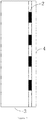
- Figure 1 shows a side view of a structure of a semiconductor detector according to an embodiment of the present invention.
- the semiconductor detector comprises a semiconductor detector material 3, which may be CZT (Cadmium zinc telluride), CdTe (cadmium telluride), CdMnTe (cadmium manganese telluride), HgI2 (mercury iodide), TIBr (thallium bromide), PbI2 (lead iodide), GaAs (gallium arsenide), Ge (germanium) and the like; an insulating material 2; and a field enhanced electrode 1.
- the field enhanced electrode may be connected to different high voltages according to the requirements of the apparatus so that the electric field distribution inside the detectors is uniform and the charge collection efficiency is increased.
- the semiconductor detector comprises: a detector crystal including a crystal body, an anode and a cathode; a field enhanced electrode 1 for applying a voltage to the detector crystal; an insulating material 2 disposed between the field enhanced electrode 1 and a surface of the detector crystal.
- the detector crystal is a tellurium zinc cadmium crystal.
- the insulating material covers an entire surface of the detector crystal at the side of the field enhanced electrode.
- the shape and size of the insulating material may be consistent with those of the field enhanced electrode. That is to say, a width of the insulating material may be equal to that of the field enhanced line electrode, may be larger than that of the field enhanced line electrode, or may cover the entire surface of a voltage applying surface of the field enhanced electrode.
- the size of the insulating material is not specifically limited here. These alternatives are illustrated in Figures 1(a), (b) and (c) , respectively.
- Figure 2 shows a schematic diagram of package structure of a field enhanced electrode circuit board according to an embodiment of the present invention.
- the present invention applies a high voltage to the field enhanced electrode by a PCB package.
- the side of the PCB board packaged with the detector is the bottom of the PCB, and the other side opposite to the back surface of the PCB is the top layer of the detector.
- the bottom layer of the PCB is a field enhanced strip electrode 1 of the detector, and there is an insulating material at a portion of the PCB where the field enhanced strip electrode 1 of the PCB is connected with the detector.
- the semiconductor detector further comprises a field enhanced electrode circuit board 4 having a bottom connection layer in contact with the surface of the detector crystal and a top layer opposite to the bottom connection layer, wherein the top layer is connected to a high voltage input terminal of the semiconductor detector, and an insulating material 2 is provided between the bottom connection layer of the field enhanced electrode circuit board and the detector surface of the detector crystal, and the field enhanced strip electrode 1 of the PCT is provided in the bottom layer of the PCB.
- the field enhanced electrode circuit board further comprises a plurality of via holes, and the top layer and the bottom connection layer are connected through via holes.
- the top layer is connected to an external high voltage source by soldering a patch socket or by a direct soldering.
- FIG 3 shows a schematic view of a top layer and a bottom layer of a field enhanced electrode circuit board 4 according to an embodiment of the present invention.
- the structure of the PCB board is shown in figure 3 .
- the top layer of the field enhanced electrode circuit board 4 comprises a high voltage interface to implement a high voltage connection.
- the top layer may further comprise a voltage dividing circuit which supplies the high voltage together with an independent power source.
- the present invention reduces the numbers of the high voltage source and shortens distance between the high voltage source and the electrodes of the detector.
- a filter circuit is provided in the top layer of the cathode circuit board, which may improve filtering effect and reduce the influence of the high voltage noise to the detector.
- the high voltage in the top layer is connected to the electrodes in the bottom layer through via holes.
- the number of via holes is not limited. There may be plenty of via holes and they are distributed in many modes.
- the design of the electrode in the bottom layer of the field enhanced electrode circuit board 4 are identical that of the field enhanced electrode of the detector in shape, and may be connected to the detector by adhesives or other connection.
- a filter circuit is provided in the high voltage side top layer of the cathode circuit board.
- the filter circuit utilizes a passive filtering.
- the filter circuit is provided at an edge of the top layer of the field enhanced electrode circuit board.
- the field enhanced electrode circuit board is a flexible circuit board.
- the filter circuit is provided in the flexible circuit board.
- the semiconductor detector and the method for packaging the same according to the present disclosure may provide an optimized field enhanced line electrode CdZnTe tellurium-zinc-cadmium semiconductor detector having a higher energy resolution and operated at room temperature, which may further improve the energy resolution of the field enhanced line electrode detector and reduce the influence of dark current.
- the invention may be applied in the fields of nuclear radiation detection, radionuclide identification, radiation imaging and nuclear technology application.
Landscapes
- Physics & Mathematics (AREA)
- Microelectronics & Electronic Packaging (AREA)
- Engineering & Computer Science (AREA)
- Spectroscopy & Molecular Physics (AREA)
- High Energy & Nuclear Physics (AREA)
- Molecular Biology (AREA)
- General Physics & Mathematics (AREA)
- Life Sciences & Earth Sciences (AREA)
- Health & Medical Sciences (AREA)
- Electromagnetism (AREA)
- Measurement Of Radiation (AREA)
- Light Receiving Elements (AREA)
- Solid State Image Pick-Up Elements (AREA)
Abstract
Description
- This application claims priority to Chinese Application No.
201610797083.0 filed at August 31, 2016 - The present disclosure relates to a semiconductor detector, and more particularly to a field-enhanced tellurium-zinc-cadmium semiconductor detector with a wire electrode.
- A field-enhanced semiconductor detector greatly improves performance of a detector such as energy resolution, peak-to-valley ratio and the like due to its uniform distribution of electric field. However, in practical applications, a high voltage of the field-enhanced electrode is directly connected to sides of the detector by usually using a direct soldering of a high-voltage line, an exposed high pressure will bring security risks, while the installation is not convenient and is not suitable for practical application. Since the high voltage source also carries noise, it increases noise of the detector and also generates a dark current between the field enhanced electrodes to affect the performance of the detector. At the same time, during a drift process of charges, the field enhanced electrode absorbs a part of signals so that a collection efficiency of anodes has been decreased.
- The object of the present invention is to further improve an energy resolution of the field-enhanced tellurium-zinc-cadmium semiconductor detector with a wire electrode, to reduce influence of a dark current in the field enhanced electrode on the detector, and to improve safety and stability of a high-voltage connection of the field-enhanced electrode.
- According to one aspect of the present invention, there is proposed a semiconductor detector, especially a field enhanced semiconductor detector.
- The semiconductor detector comprises: a detector crystal including a crystal body, an anode and a cathode; a field enhance electrode for applying a voltage to the detector crystal; an insulating material disposed between the field enhanced electrode and a surface of the detector crystal.
- Preferably, the insulating material covers an entire surface of the detector crystal at the side of the field enhanced electrode.
- Preferably, the detector crystal is a tellurium zinc cadmium crystal.
- Preferably, the semiconductor detector further comprises a field enhanced electrode circuit board having a bottom connection layer in contact with the surface of the detector crystal and a top layer opposite to the bottom connection layer, wherein the top layer is connected to a high voltage input terminal of the semiconductor detector, and an insulating material is provided between the bottom connection layer and the detector surface of the detector crystal.
- Preferably, the field enhanced electrode circuit board further comprises a plurality of via holes, and the top layer is connected to the bottom connection layer through the via holes.
- Preferably, the top layer is connected to an external high voltage source by soldering a patch socket or by a direct soldering.
- Preferably, a filter circuit is provided in the high voltage side top layer of the cathode circuit board.
- Preferably, the filter circuit utilizes a passive filtering.
- Preferably, the filter circuit is provided at an edge of the top layer of the field enhanced electrode circuit board.
- Preferably, the field enhanced electrode circuit board is a flexible circuit board.
- Preferably, the filter circuit is provided in the flexible circuit board.
- Preferably, a voltage dividing circuit is further provided in the top layer, and the voltage dividing circuit supplies power to the field enhanced electrode circuit board together with an independent power source.
- The invention adds the insulating material between the field enhanced electrodes and prevents the high voltage noise from entering the detector crystal while providing a uniform electric field for the detector, and prevent the signal in the blocking detector from being absorbed by the field enhanced electrode.
- The invention also utilizes a PCB package to provide high voltage to the field enhanced electrode, and the voltage dividing circuit reduces the numbers of the high voltage source. The filter circuit improves a signal to noise ratio of the high voltage, shortens the distance between the detector electrodes, and enhances energy resolution of the detector.
- The semiconductor detector and the method for packaging the same according to the present disclosure may provide an optimized field enhanced line electrode CdZnTe tellurium-zinc-cadmium semiconductor detector having a higher energy resolution and operated at room temperature, which may further improve the energy resolution of the field enhanced line electrode detector and reduce the influence of dark current. The invention may be applied in the fields of nuclear radiation detection, radionuclide identification, radiation imaging and nuclear technology application.
-
-
Figure 1 shows a side view of a structure of a semiconductor detector according to an embodiment of the present invention; -
Figure 2 shows a schematic diagram of package structure of a field enhanced electrode circuit board according to an embodiment of the present invention; -
Figure 3 shows a schematic view of a top layer and a bottom layer of a field enhanced electrode circuit board according to an embodiment of the present invention. - Reference will now be made to the embodiments of the present invention, examples of which are illustrated in the accompanying drawings, wherein like reference numerals refer to similar elements throughout the drawings. The following examples of the present invention will be described with reference to the accompanying drawings.
- The present invention adds the insulating material between the field enhanced electrode and the surface of the detector, which may reduce influence of the high voltage noise of the side field enhanced to the detector, reduces the dark current between the field enhanced electrodes and improve the energy resolution of the detector.
-
Figure 1 shows a side view of a structure of a semiconductor detector according to an embodiment of the present invention. As shown infigure 1 , the semiconductor detector comprises asemiconductor detector material 3, which may be CZT (Cadmium zinc telluride), CdTe (cadmium telluride), CdMnTe (cadmium manganese telluride), HgI2 (mercury iodide), TIBr (thallium bromide), PbI2 (lead iodide), GaAs (gallium arsenide), Ge (germanium) and the like; aninsulating material 2; and a field enhanced electrode 1. The field enhanced electrode may be connected to different high voltages according to the requirements of the apparatus so that the electric field distribution inside the detectors is uniform and the charge collection efficiency is increased. - In particular, the semiconductor detector comprises: a detector crystal including a crystal body, an anode and a cathode; a field enhanced electrode 1 for applying a voltage to the detector crystal; an
insulating material 2 disposed between the field enhanced electrode 1 and a surface of the detector crystal. - Preferably, the detector crystal is a tellurium zinc cadmium crystal.
- Optionally, the insulating material covers an entire surface of the detector crystal at the side of the field enhanced electrode. The shape and size of the insulating material may be consistent with those of the field enhanced electrode. That is to say, a width of the insulating material may be equal to that of the field enhanced line electrode, may be larger than that of the field enhanced line electrode, or may cover the entire surface of a voltage applying surface of the field enhanced electrode. The size of the insulating material is not specifically limited here. These alternatives are illustrated in
Figures 1(a), (b) and (c) , respectively. - In the existing semiconductor detectors, it is necessary to solder the high voltage terminal to the field enhanced electrode of the detector through the high-voltage wire, and it should be very careful for the soldering and bring inconvenience to the use of the detector. The high-voltage wire will be broken in use and damage the detector.
-
Figure 2 shows a schematic diagram of package structure of a field enhanced electrode circuit board according to an embodiment of the present invention. The present invention applies a high voltage to the field enhanced electrode by a PCB package. In this way, the side of the PCB board packaged with the detector is the bottom of the PCB, and the other side opposite to the back surface of the PCB is the top layer of the detector. The bottom layer of the PCB is a field enhanced strip electrode 1 of the detector, and there is an insulating material at a portion of the PCB where the field enhanced strip electrode 1 of the PCB is connected with the detector. In particular, the semiconductor detector further comprises a field enhancedelectrode circuit board 4 having a bottom connection layer in contact with the surface of the detector crystal and a top layer opposite to the bottom connection layer, wherein the top layer is connected to a high voltage input terminal of the semiconductor detector, and aninsulating material 2 is provided between the bottom connection layer of the field enhanced electrode circuit board and the detector surface of the detector crystal, and the field enhanced strip electrode 1 of the PCT is provided in the bottom layer of the PCB. - The field enhanced electrode circuit board further comprises a plurality of via holes, and the top layer and the bottom connection layer are connected through via holes. The top layer is connected to an external high voltage source by soldering a patch socket or by a direct soldering.
-
Figure 3 shows a schematic view of a top layer and a bottom layer of a field enhancedelectrode circuit board 4 according to an embodiment of the present invention. The structure of the PCB board is shown infigure 3 . The top layer of the field enhancedelectrode circuit board 4 comprises a high voltage interface to implement a high voltage connection. The top layer may further comprise a voltage dividing circuit which supplies the high voltage together with an independent power source. The present invention reduces the numbers of the high voltage source and shortens distance between the high voltage source and the electrodes of the detector. A filter circuit is provided in the top layer of the cathode circuit board, which may improve filtering effect and reduce the influence of the high voltage noise to the detector. The high voltage in the top layer is connected to the electrodes in the bottom layer through via holes. The number of via holes is not limited. There may be plenty of via holes and they are distributed in many modes. The design of the electrode in the bottom layer of the field enhancedelectrode circuit board 4 are identical that of the field enhanced electrode of the detector in shape, and may be connected to the detector by adhesives or other connection. - In particular, a filter circuit is provided in the high voltage side top layer of the cathode circuit board. The filter circuit utilizes a passive filtering. The filter circuit is provided at an edge of the top layer of the field enhanced electrode circuit board. The field enhanced electrode circuit board is a flexible circuit board. The filter circuit is provided in the flexible circuit board.
- The semiconductor detector and the method for packaging the same according to the present disclosure may provide an optimized field enhanced line electrode CdZnTe tellurium-zinc-cadmium semiconductor detector having a higher energy resolution and operated at room temperature, which may further improve the energy resolution of the field enhanced line electrode detector and reduce the influence of dark current. The invention may be applied in the fields of nuclear radiation detection, radionuclide identification, radiation imaging and nuclear technology application.
- Although the present invention has been particularly shown and described with reference to exemplary embodiments thereof, it will be understood by those skilled in the art that various changes and modifications in form and detail may be made without departing from spirit and scope of the invention as defined by the appended claims.
Claims (12)
- A semiconductor detector comprising:a detector crystal including a crystal body, an anode and a cathode;a field enhance electrode for applying a voltage to the detector crystal;an insulating material disposed between the field enhanced electrode and a surface of the detector crystal.
- The semiconductor detector according to claim 1, wherein the insulating material covers an entire surface of the detector crystal at the side of the field enhanced electrode.
- The semiconductor detector according to claim 1, wherein the detector crystal is a tellurium zinc cadmium crystal.
- The semiconductor detector according to claim 1, further comprising a field enhanced electrode circuit board having a bottom connection layer in contact with the surface of the detector crystal and a top layer opposite to the bottom connection layer, wherein the top layer is connected to a high voltage input terminal of the semiconductor detector, and an insulating material is provided between the bottom connection layer and the detector surface of the detector crystal.
- The semiconductor detector according to claim 4, wherein the field enhanced electrode circuit board further comprises a plurality of via holes, and the top layer is connected to the bottom connection layer through the via holes.
- The semiconductor detector according to claim 1, wherein the top layer is connected to an external high voltage source by soldering a patch socket or by a direct soldering.
- The semiconductor detector according to claim 1, wherein a filter circuit is provided in the high voltage side top layer of the cathode circuit board.
- The semiconductor detector according to claim 7, wherein the filter circuit utilizes a passive filtering.
- The semiconductor detector according to claim 7, wherein the filter circuit is provided at an edge of the top layer of the field enhanced electrode circuit board.
- The semiconductor detector according to claim 4, wherein the field enhanced electrode circuit board is a flexible circuit board.
- The semiconductor detector according to claim 10, wherein the filter circuit is provided in the flexible circuit board.
- The semiconductor detector according to claim 4, wherein a voltage dividing circuit is further provided in the top layer, and the voltage dividing circuit supplies power to the field enhanced electrode circuit board together with an independent power source.
Applications Claiming Priority (1)
| Application Number | Priority Date | Filing Date | Title |
|---|---|---|---|
| CN201610797083.0A CN106249269B (en) | 2016-08-31 | 2016-08-31 | semiconductor detector |
Publications (2)
| Publication Number | Publication Date |
|---|---|
| EP3291311A1 true EP3291311A1 (en) | 2018-03-07 |
| EP3291311B1 EP3291311B1 (en) | 2024-08-14 |
Family
ID=58080106
Family Applications (1)
| Application Number | Title | Priority Date | Filing Date |
|---|---|---|---|
| EP17188640.1A Active EP3291311B1 (en) | 2016-08-31 | 2017-08-30 | Semiconductor detector |
Country Status (3)
| Country | Link |
|---|---|
| US (1) | US10101473B2 (en) |
| EP (1) | EP3291311B1 (en) |
| CN (1) | CN106249269B (en) |
Families Citing this family (1)
| Publication number | Priority date | Publication date | Assignee | Title |
|---|---|---|---|---|
| US10558659B2 (en) | 2016-09-16 | 2020-02-11 | Oracle International Corporation | Techniques for dictionary based join and aggregation |
Citations (5)
| Publication number | Priority date | Publication date | Assignee | Title |
|---|---|---|---|---|
| US6472668B1 (en) * | 2000-11-24 | 2002-10-29 | Koninklijke Philips Electronics N.V. | High voltage distribution system for CZT arrays |
| US20050247880A1 (en) * | 2004-05-04 | 2005-11-10 | Wear James A | Solid-state X-ray detector with support mounted steering electrodes |
| US7223982B1 (en) * | 2006-02-22 | 2007-05-29 | Redlen Technologies | Segmented radiation detector with side shielding cathode |
| US20110049376A1 (en) * | 2009-08-31 | 2011-03-03 | General Electric Company | Semiconductor crystal based radiation detector and method of producing the same |
| US20160240584A1 (en) * | 2015-02-17 | 2016-08-18 | Redlen Technologies, Inc. | High-performance radiation detectors and methods of fabricating thereof |
Family Cites Families (6)
| Publication number | Priority date | Publication date | Assignee | Title |
|---|---|---|---|---|
| CN101960591A (en) * | 2008-03-28 | 2011-01-26 | 日本电气株式会社 | Semiconductor device, semiconductor device manufacturing method, printed circuit board and electronic device |
| JP5155808B2 (en) * | 2008-10-08 | 2013-03-06 | 株式会社日立製作所 | Semiconductor radiation detector and nuclear medicine diagnostic equipment |
| CN103913763B (en) * | 2013-01-07 | 2016-06-15 | 同方威视技术股份有限公司 | Radiation detector and radiation detector assembly |
| CN103972323B (en) * | 2013-01-31 | 2017-05-03 | 同方威视技术股份有限公司 | Radiation detector |
| CN103393420B (en) * | 2013-07-30 | 2015-06-17 | 中国科学技术大学 | High-density active flexible electrode array and signal conditioning circuit thereof |
| CN104111470A (en) * | 2014-07-15 | 2014-10-22 | 清华大学 | Method and device for signal processing of semiconductor detector |
-
2016
- 2016-08-31 CN CN201610797083.0A patent/CN106249269B/en active Active
-
2017
- 2017-05-26 US US15/606,071 patent/US10101473B2/en not_active Expired - Fee Related
- 2017-08-30 EP EP17188640.1A patent/EP3291311B1/en active Active
Patent Citations (5)
| Publication number | Priority date | Publication date | Assignee | Title |
|---|---|---|---|---|
| US6472668B1 (en) * | 2000-11-24 | 2002-10-29 | Koninklijke Philips Electronics N.V. | High voltage distribution system for CZT arrays |
| US20050247880A1 (en) * | 2004-05-04 | 2005-11-10 | Wear James A | Solid-state X-ray detector with support mounted steering electrodes |
| US7223982B1 (en) * | 2006-02-22 | 2007-05-29 | Redlen Technologies | Segmented radiation detector with side shielding cathode |
| US20110049376A1 (en) * | 2009-08-31 | 2011-03-03 | General Electric Company | Semiconductor crystal based radiation detector and method of producing the same |
| US20160240584A1 (en) * | 2015-02-17 | 2016-08-18 | Redlen Technologies, Inc. | High-performance radiation detectors and methods of fabricating thereof |
Also Published As
| Publication number | Publication date |
|---|---|
| US20180059261A1 (en) | 2018-03-01 |
| EP3291311B1 (en) | 2024-08-14 |
| US10101473B2 (en) | 2018-10-16 |
| CN106249269B (en) | 2023-05-23 |
| CN106249269A (en) | 2016-12-21 |
Similar Documents
| Publication | Publication Date | Title |
|---|---|---|
| JP6167501B2 (en) | Radiation imaging equipment | |
| KR101640108B1 (en) | X-ray radiation detector and ct system | |
| EP2762924A2 (en) | Radiation detectors | |
| CN105280659A (en) | Imaging device for electromagnetic radiation | |
| CN110637377A (en) | X-ray sensor with detector diode and junction termination structure | |
| EP3174108A1 (en) | A quantum dot photodetector apparatus and associated methods | |
| JP2014508567A5 (en) | ||
| JPWO2011104991A1 (en) | Radiation imaging equipment | |
| JP5332619B2 (en) | Portable radiographic imaging device and radiographic imaging system | |
| US10502842B2 (en) | Radiation detector | |
| EP3291311B1 (en) | Semiconductor detector | |
| WO2008108995A1 (en) | Electric field steering cap, steering electrode, and modular configurations for a radiation detector | |
| US10670743B2 (en) | Semiconductor detector and method for packaging the same | |
| EP2796897B1 (en) | Semiconductor detector | |
| US9613992B2 (en) | Detector module for an imaging system | |
| EP3079174B1 (en) | X-ray detector, x-ray imaging device using same, and driving method therefor | |
| JP5099000B2 (en) | Portable radiographic imaging device and radiographic imaging system | |
| US20100163741A1 (en) | Radiation detector | |
| CN206387912U (en) | Semiconductor detector | |
| CN102414580B (en) | Radiation detector | |
| JP6241066B2 (en) | Radiation imaging equipment | |
| US20120080601A1 (en) | Apparatus and method for detecting radiation | |
| JP2011035215A (en) | Radiation image photographing device | |
| KR20160018271A (en) | Radiation detector | |
| RU2020107899A (en) | NUCLEAR MICROBATTERY |
Legal Events
| Date | Code | Title | Description |
|---|---|---|---|
| PUAI | Public reference made under article 153(3) epc to a published international application that has entered the european phase |
Free format text: ORIGINAL CODE: 0009012 |
|
| STAA | Information on the status of an ep patent application or granted ep patent |
Free format text: STATUS: REQUEST FOR EXAMINATION WAS MADE |
|
| 17P | Request for examination filed |
Effective date: 20170831 |
|
| AK | Designated contracting states |
Kind code of ref document: A1 Designated state(s): AL AT BE BG CH CY CZ DE DK EE ES FI FR GB GR HR HU IE IS IT LI LT LU LV MC MK MT NL NO PL PT RO RS SE SI SK SM TR |
|
| AX | Request for extension of the european patent |
Extension state: BA ME |
|
| STAA | Information on the status of an ep patent application or granted ep patent |
Free format text: STATUS: EXAMINATION IS IN PROGRESS |
|
| 17Q | First examination report despatched |
Effective date: 20200421 |
|
| GRAP | Despatch of communication of intention to grant a patent |
Free format text: ORIGINAL CODE: EPIDOSNIGR1 |
|
| STAA | Information on the status of an ep patent application or granted ep patent |
Free format text: STATUS: GRANT OF PATENT IS INTENDED |
|
| INTG | Intention to grant announced |
Effective date: 20240314 |
|
| GRAS | Grant fee paid |
Free format text: ORIGINAL CODE: EPIDOSNIGR3 |
|
| GRAA | (expected) grant |
Free format text: ORIGINAL CODE: 0009210 |
|
| STAA | Information on the status of an ep patent application or granted ep patent |
Free format text: STATUS: THE PATENT HAS BEEN GRANTED |
|
| AK | Designated contracting states |
Kind code of ref document: B1 Designated state(s): AL AT BE BG CH CY CZ DE DK EE ES FI FR GB GR HR HU IE IS IT LI LT LU LV MC MK MT NL NO PL PT RO RS SE SI SK SM TR |
|
| REG | Reference to a national code |
Ref country code: GB Ref legal event code: FG4D |
|
| REG | Reference to a national code |
Ref country code: CH Ref legal event code: EP |
|
| REG | Reference to a national code |
Ref country code: DE Ref legal event code: R096 Ref document number: 602017084030 Country of ref document: DE |
|
| REG | Reference to a national code |
Ref country code: IE Ref legal event code: FG4D |
|
| REG | Reference to a national code |
Ref country code: DE Ref legal event code: R079 Ref document number: 602017084030 Country of ref document: DE Free format text: PREVIOUS MAIN CLASS: H01L0031022400 Ipc: H10F0077200000 |
|
| REG | Reference to a national code |
Ref country code: LT Ref legal event code: MG9D |
|
| REG | Reference to a national code |
Ref country code: NL Ref legal event code: MP Effective date: 20240814 |
|
| PG25 | Lapsed in a contracting state [announced via postgrant information from national office to epo] |
Ref country code: NO Free format text: LAPSE BECAUSE OF FAILURE TO SUBMIT A TRANSLATION OF THE DESCRIPTION OR TO PAY THE FEE WITHIN THE PRESCRIBED TIME-LIMIT Effective date: 20241114 |
|
| REG | Reference to a national code |
Ref country code: AT Ref legal event code: MK05 Ref document number: 1714123 Country of ref document: AT Kind code of ref document: T Effective date: 20240814 |
|
| PG25 | Lapsed in a contracting state [announced via postgrant information from national office to epo] |
Ref country code: GR Free format text: LAPSE BECAUSE OF FAILURE TO SUBMIT A TRANSLATION OF THE DESCRIPTION OR TO PAY THE FEE WITHIN THE PRESCRIBED TIME-LIMIT Effective date: 20241115 Ref country code: FI Free format text: LAPSE BECAUSE OF FAILURE TO SUBMIT A TRANSLATION OF THE DESCRIPTION OR TO PAY THE FEE WITHIN THE PRESCRIBED TIME-LIMIT Effective date: 20240814 Ref country code: NL Free format text: LAPSE BECAUSE OF FAILURE TO SUBMIT A TRANSLATION OF THE DESCRIPTION OR TO PAY THE FEE WITHIN THE PRESCRIBED TIME-LIMIT Effective date: 20240814 Ref country code: PT Free format text: LAPSE BECAUSE OF FAILURE TO SUBMIT A TRANSLATION OF THE DESCRIPTION OR TO PAY THE FEE WITHIN THE PRESCRIBED TIME-LIMIT Effective date: 20241216 Ref country code: PL Free format text: LAPSE BECAUSE OF FAILURE TO SUBMIT A TRANSLATION OF THE DESCRIPTION OR TO PAY THE FEE WITHIN THE PRESCRIBED TIME-LIMIT Effective date: 20240814 |
|
| PG25 | Lapsed in a contracting state [announced via postgrant information from national office to epo] |
Ref country code: BG Free format text: LAPSE BECAUSE OF FAILURE TO SUBMIT A TRANSLATION OF THE DESCRIPTION OR TO PAY THE FEE WITHIN THE PRESCRIBED TIME-LIMIT Effective date: 20240814 |
|
| PG25 | Lapsed in a contracting state [announced via postgrant information from national office to epo] |
Ref country code: LV Free format text: LAPSE BECAUSE OF FAILURE TO SUBMIT A TRANSLATION OF THE DESCRIPTION OR TO PAY THE FEE WITHIN THE PRESCRIBED TIME-LIMIT Effective date: 20240814 |
|
| PG25 | Lapsed in a contracting state [announced via postgrant information from national office to epo] |
Ref country code: AT Free format text: LAPSE BECAUSE OF FAILURE TO SUBMIT A TRANSLATION OF THE DESCRIPTION OR TO PAY THE FEE WITHIN THE PRESCRIBED TIME-LIMIT Effective date: 20240814 Ref country code: IS Free format text: LAPSE BECAUSE OF FAILURE TO SUBMIT A TRANSLATION OF THE DESCRIPTION OR TO PAY THE FEE WITHIN THE PRESCRIBED TIME-LIMIT Effective date: 20241214 |
|
| PG25 | Lapsed in a contracting state [announced via postgrant information from national office to epo] |
Ref country code: HR Free format text: LAPSE BECAUSE OF FAILURE TO SUBMIT A TRANSLATION OF THE DESCRIPTION OR TO PAY THE FEE WITHIN THE PRESCRIBED TIME-LIMIT Effective date: 20240814 |
|
| PG25 | Lapsed in a contracting state [announced via postgrant information from national office to epo] |
Ref country code: ES Free format text: LAPSE BECAUSE OF FAILURE TO SUBMIT A TRANSLATION OF THE DESCRIPTION OR TO PAY THE FEE WITHIN THE PRESCRIBED TIME-LIMIT Effective date: 20240814 Ref country code: RS Free format text: LAPSE BECAUSE OF FAILURE TO SUBMIT A TRANSLATION OF THE DESCRIPTION OR TO PAY THE FEE WITHIN THE PRESCRIBED TIME-LIMIT Effective date: 20241114 |
|
| PG25 | Lapsed in a contracting state [announced via postgrant information from national office to epo] |
Ref country code: RS Free format text: LAPSE BECAUSE OF FAILURE TO SUBMIT A TRANSLATION OF THE DESCRIPTION OR TO PAY THE FEE WITHIN THE PRESCRIBED TIME-LIMIT Effective date: 20241114 Ref country code: PT Free format text: LAPSE BECAUSE OF FAILURE TO SUBMIT A TRANSLATION OF THE DESCRIPTION OR TO PAY THE FEE WITHIN THE PRESCRIBED TIME-LIMIT Effective date: 20241216 Ref country code: PL Free format text: LAPSE BECAUSE OF FAILURE TO SUBMIT A TRANSLATION OF THE DESCRIPTION OR TO PAY THE FEE WITHIN THE PRESCRIBED TIME-LIMIT Effective date: 20240814 Ref country code: NO Free format text: LAPSE BECAUSE OF FAILURE TO SUBMIT A TRANSLATION OF THE DESCRIPTION OR TO PAY THE FEE WITHIN THE PRESCRIBED TIME-LIMIT Effective date: 20241114 Ref country code: NL Free format text: LAPSE BECAUSE OF FAILURE TO SUBMIT A TRANSLATION OF THE DESCRIPTION OR TO PAY THE FEE WITHIN THE PRESCRIBED TIME-LIMIT Effective date: 20240814 Ref country code: LV Free format text: LAPSE BECAUSE OF FAILURE TO SUBMIT A TRANSLATION OF THE DESCRIPTION OR TO PAY THE FEE WITHIN THE PRESCRIBED TIME-LIMIT Effective date: 20240814 Ref country code: IS Free format text: LAPSE BECAUSE OF FAILURE TO SUBMIT A TRANSLATION OF THE DESCRIPTION OR TO PAY THE FEE WITHIN THE PRESCRIBED TIME-LIMIT Effective date: 20241214 Ref country code: HR Free format text: LAPSE BECAUSE OF FAILURE TO SUBMIT A TRANSLATION OF THE DESCRIPTION OR TO PAY THE FEE WITHIN THE PRESCRIBED TIME-LIMIT Effective date: 20240814 Ref country code: GR Free format text: LAPSE BECAUSE OF FAILURE TO SUBMIT A TRANSLATION OF THE DESCRIPTION OR TO PAY THE FEE WITHIN THE PRESCRIBED TIME-LIMIT Effective date: 20241115 Ref country code: FI Free format text: LAPSE BECAUSE OF FAILURE TO SUBMIT A TRANSLATION OF THE DESCRIPTION OR TO PAY THE FEE WITHIN THE PRESCRIBED TIME-LIMIT Effective date: 20240814 Ref country code: ES Free format text: LAPSE BECAUSE OF FAILURE TO SUBMIT A TRANSLATION OF THE DESCRIPTION OR TO PAY THE FEE WITHIN THE PRESCRIBED TIME-LIMIT Effective date: 20240814 Ref country code: BG Free format text: LAPSE BECAUSE OF FAILURE TO SUBMIT A TRANSLATION OF THE DESCRIPTION OR TO PAY THE FEE WITHIN THE PRESCRIBED TIME-LIMIT Effective date: 20240814 Ref country code: AT Free format text: LAPSE BECAUSE OF FAILURE TO SUBMIT A TRANSLATION OF THE DESCRIPTION OR TO PAY THE FEE WITHIN THE PRESCRIBED TIME-LIMIT Effective date: 20240814 |
|
| REG | Reference to a national code |
Ref country code: DE Ref legal event code: R119 Ref document number: 602017084030 Country of ref document: DE |
|
| REG | Reference to a national code |
Ref country code: CH Ref legal event code: PL |
|
| PG25 | Lapsed in a contracting state [announced via postgrant information from national office to epo] |
Ref country code: RO Free format text: LAPSE BECAUSE OF FAILURE TO SUBMIT A TRANSLATION OF THE DESCRIPTION OR TO PAY THE FEE WITHIN THE PRESCRIBED TIME-LIMIT Effective date: 20240814 Ref country code: SM Free format text: LAPSE BECAUSE OF FAILURE TO SUBMIT A TRANSLATION OF THE DESCRIPTION OR TO PAY THE FEE WITHIN THE PRESCRIBED TIME-LIMIT Effective date: 20240814 Ref country code: DK Free format text: LAPSE BECAUSE OF FAILURE TO SUBMIT A TRANSLATION OF THE DESCRIPTION OR TO PAY THE FEE WITHIN THE PRESCRIBED TIME-LIMIT Effective date: 20240814 |
|
| PG25 | Lapsed in a contracting state [announced via postgrant information from national office to epo] |
Ref country code: LU Free format text: LAPSE BECAUSE OF NON-PAYMENT OF DUE FEES Effective date: 20240830 |
|
| PG25 | Lapsed in a contracting state [announced via postgrant information from national office to epo] |
Ref country code: EE Free format text: LAPSE BECAUSE OF FAILURE TO SUBMIT A TRANSLATION OF THE DESCRIPTION OR TO PAY THE FEE WITHIN THE PRESCRIBED TIME-LIMIT Effective date: 20240814 Ref country code: CH Free format text: LAPSE BECAUSE OF NON-PAYMENT OF DUE FEES Effective date: 20240831 |
|
| PG25 | Lapsed in a contracting state [announced via postgrant information from national office to epo] |
Ref country code: CZ Free format text: LAPSE BECAUSE OF FAILURE TO SUBMIT A TRANSLATION OF THE DESCRIPTION OR TO PAY THE FEE WITHIN THE PRESCRIBED TIME-LIMIT Effective date: 20240814 |
|
| PG25 | Lapsed in a contracting state [announced via postgrant information from national office to epo] |
Ref country code: SK Free format text: LAPSE BECAUSE OF FAILURE TO SUBMIT A TRANSLATION OF THE DESCRIPTION OR TO PAY THE FEE WITHIN THE PRESCRIBED TIME-LIMIT Effective date: 20240814 Ref country code: IT Free format text: LAPSE BECAUSE OF FAILURE TO SUBMIT A TRANSLATION OF THE DESCRIPTION OR TO PAY THE FEE WITHIN THE PRESCRIBED TIME-LIMIT Effective date: 20240814 |
|
| PLBE | No opposition filed within time limit |
Free format text: ORIGINAL CODE: 0009261 |
|
| STAA | Information on the status of an ep patent application or granted ep patent |
Free format text: STATUS: NO OPPOSITION FILED WITHIN TIME LIMIT |
|
| REG | Reference to a national code |
Ref country code: BE Ref legal event code: MM Effective date: 20240831 |
|
| PG25 | Lapsed in a contracting state [announced via postgrant information from national office to epo] |
Ref country code: MC Free format text: LAPSE BECAUSE OF FAILURE TO SUBMIT A TRANSLATION OF THE DESCRIPTION OR TO PAY THE FEE WITHIN THE PRESCRIBED TIME-LIMIT Effective date: 20240814 |
|
| PG25 | Lapsed in a contracting state [announced via postgrant information from national office to epo] |
Ref country code: DE Free format text: LAPSE BECAUSE OF NON-PAYMENT OF DUE FEES Effective date: 20250301 |
|
| PG25 | Lapsed in a contracting state [announced via postgrant information from national office to epo] |
Ref country code: BE Free format text: LAPSE BECAUSE OF NON-PAYMENT OF DUE FEES Effective date: 20240831 |
|
| PG25 | Lapsed in a contracting state [announced via postgrant information from national office to epo] |
Ref country code: FR Free format text: LAPSE BECAUSE OF NON-PAYMENT OF DUE FEES Effective date: 20241014 |
|
| 26N | No opposition filed |
Effective date: 20250515 |
|
| GBPC | Gb: european patent ceased through non-payment of renewal fee |
Effective date: 20241114 |
|
| PG25 | Lapsed in a contracting state [announced via postgrant information from national office to epo] |
Ref country code: IE Free format text: LAPSE BECAUSE OF NON-PAYMENT OF DUE FEES Effective date: 20240830 |
|
| PG25 | Lapsed in a contracting state [announced via postgrant information from national office to epo] |
Ref country code: SE Free format text: LAPSE BECAUSE OF FAILURE TO SUBMIT A TRANSLATION OF THE DESCRIPTION OR TO PAY THE FEE WITHIN THE PRESCRIBED TIME-LIMIT Effective date: 20240814 |
|
| PG25 | Lapsed in a contracting state [announced via postgrant information from national office to epo] |
Ref country code: GB Free format text: LAPSE BECAUSE OF NON-PAYMENT OF DUE FEES Effective date: 20241114 |
|
| PG25 | Lapsed in a contracting state [announced via postgrant information from national office to epo] |
Ref country code: CY Free format text: LAPSE BECAUSE OF FAILURE TO SUBMIT A TRANSLATION OF THE DESCRIPTION OR TO PAY THE FEE WITHIN THE PRESCRIBED TIME-LIMIT; INVALID AB INITIO Effective date: 20170830 |
|
| PG25 | Lapsed in a contracting state [announced via postgrant information from national office to epo] |
Ref country code: HU Free format text: LAPSE BECAUSE OF FAILURE TO SUBMIT A TRANSLATION OF THE DESCRIPTION OR TO PAY THE FEE WITHIN THE PRESCRIBED TIME-LIMIT; INVALID AB INITIO Effective date: 20170830 |
|
| PG25 | Lapsed in a contracting state [announced via postgrant information from national office to epo] |
Ref country code: TR Free format text: LAPSE BECAUSE OF FAILURE TO SUBMIT A TRANSLATION OF THE DESCRIPTION OR TO PAY THE FEE WITHIN THE PRESCRIBED TIME-LIMIT Effective date: 20240814 |
|
| PG25 | Lapsed in a contracting state [announced via postgrant information from national office to epo] |
Ref country code: SI Free format text: LAPSE BECAUSE OF FAILURE TO SUBMIT A TRANSLATION OF THE DESCRIPTION OR TO PAY THE FEE WITHIN THE PRESCRIBED TIME-LIMIT Effective date: 20240814 |
|
| PG25 | Lapsed in a contracting state [announced via postgrant information from national office to epo] |
Ref country code: LT Free format text: LAPSE BECAUSE OF FAILURE TO SUBMIT A TRANSLATION OF THE DESCRIPTION OR TO PAY THE FEE WITHIN THE PRESCRIBED TIME-LIMIT Effective date: 20240814 |