EP3291301A1 - Organic light-emitting display device having a partition wall - Google Patents
Organic light-emitting display device having a partition wall Download PDFInfo
- Publication number
- EP3291301A1 EP3291301A1 EP17188644.3A EP17188644A EP3291301A1 EP 3291301 A1 EP3291301 A1 EP 3291301A1 EP 17188644 A EP17188644 A EP 17188644A EP 3291301 A1 EP3291301 A1 EP 3291301A1
- Authority
- EP
- European Patent Office
- Prior art keywords
- insulating layer
- bank insulating
- organic light
- display device
- emitting display
- Prior art date
- Legal status (The legal status is an assumption and is not a legal conclusion. Google has not performed a legal analysis and makes no representation as to the accuracy of the status listed.)
- Granted
Links
Images



Classifications
-
- H—ELECTRICITY
- H10—SEMICONDUCTOR DEVICES; ELECTRIC SOLID-STATE DEVICES NOT OTHERWISE PROVIDED FOR
- H10K—ORGANIC ELECTRIC SOLID-STATE DEVICES
- H10K50/00—Organic light-emitting devices
- H10K50/80—Constructional details
- H10K50/84—Passivation; Containers; Encapsulations
- H10K50/841—Self-supporting sealing arrangements
-
- H—ELECTRICITY
- H10—SEMICONDUCTOR DEVICES; ELECTRIC SOLID-STATE DEVICES NOT OTHERWISE PROVIDED FOR
- H10K—ORGANIC ELECTRIC SOLID-STATE DEVICES
- H10K50/00—Organic light-emitting devices
- H10K50/80—Constructional details
- H10K50/805—Electrodes
- H10K50/81—Anodes
- H10K50/813—Anodes characterised by their shape
-
- H—ELECTRICITY
- H10—SEMICONDUCTOR DEVICES; ELECTRIC SOLID-STATE DEVICES NOT OTHERWISE PROVIDED FOR
- H10K—ORGANIC ELECTRIC SOLID-STATE DEVICES
- H10K50/00—Organic light-emitting devices
- H10K50/80—Constructional details
- H10K50/805—Electrodes
- H10K50/81—Anodes
- H10K50/814—Anodes combined with auxiliary electrodes, e.g. ITO layer combined with metal lines
-
- H—ELECTRICITY
- H10—SEMICONDUCTOR DEVICES; ELECTRIC SOLID-STATE DEVICES NOT OTHERWISE PROVIDED FOR
- H10K—ORGANIC ELECTRIC SOLID-STATE DEVICES
- H10K50/00—Organic light-emitting devices
- H10K50/80—Constructional details
- H10K50/805—Electrodes
- H10K50/82—Cathodes
- H10K50/824—Cathodes combined with auxiliary electrodes
-
- H—ELECTRICITY
- H10—SEMICONDUCTOR DEVICES; ELECTRIC SOLID-STATE DEVICES NOT OTHERWISE PROVIDED FOR
- H10K—ORGANIC ELECTRIC SOLID-STATE DEVICES
- H10K50/00—Organic light-emitting devices
- H10K50/80—Constructional details
- H10K50/84—Passivation; Containers; Encapsulations
-
- H—ELECTRICITY
- H10—SEMICONDUCTOR DEVICES; ELECTRIC SOLID-STATE DEVICES NOT OTHERWISE PROVIDED FOR
- H10K—ORGANIC ELECTRIC SOLID-STATE DEVICES
- H10K50/00—Organic light-emitting devices
- H10K50/80—Constructional details
- H10K50/84—Passivation; Containers; Encapsulations
- H10K50/842—Containers
- H10K50/8428—Vertical spacers, e.g. arranged between the sealing arrangement and the OLED
-
- H—ELECTRICITY
- H10—SEMICONDUCTOR DEVICES; ELECTRIC SOLID-STATE DEVICES NOT OTHERWISE PROVIDED FOR
- H10K—ORGANIC ELECTRIC SOLID-STATE DEVICES
- H10K59/00—Integrated devices, or assemblies of multiple devices, comprising at least one organic light-emitting element covered by group H10K50/00
- H10K59/10—OLED displays
- H10K59/12—Active-matrix OLED [AMOLED] displays
- H10K59/122—Pixel-defining structures or layers, e.g. banks
-
- H—ELECTRICITY
- H10—SEMICONDUCTOR DEVICES; ELECTRIC SOLID-STATE DEVICES NOT OTHERWISE PROVIDED FOR
- H10K—ORGANIC ELECTRIC SOLID-STATE DEVICES
- H10K59/00—Integrated devices, or assemblies of multiple devices, comprising at least one organic light-emitting element covered by group H10K50/00
- H10K59/80—Constructional details
- H10K59/805—Electrodes
- H10K59/8051—Anodes
- H10K59/80515—Anodes characterised by their shape
-
- H—ELECTRICITY
- H10—SEMICONDUCTOR DEVICES; ELECTRIC SOLID-STATE DEVICES NOT OTHERWISE PROVIDED FOR
- H10K—ORGANIC ELECTRIC SOLID-STATE DEVICES
- H10K59/00—Integrated devices, or assemblies of multiple devices, comprising at least one organic light-emitting element covered by group H10K50/00
- H10K59/80—Constructional details
- H10K59/805—Electrodes
- H10K59/8051—Anodes
- H10K59/80516—Anodes combined with auxiliary electrodes, e.g. ITO layer combined with metal lines
-
- H—ELECTRICITY
- H10—SEMICONDUCTOR DEVICES; ELECTRIC SOLID-STATE DEVICES NOT OTHERWISE PROVIDED FOR
- H10K—ORGANIC ELECTRIC SOLID-STATE DEVICES
- H10K59/00—Integrated devices, or assemblies of multiple devices, comprising at least one organic light-emitting element covered by group H10K50/00
- H10K59/80—Constructional details
- H10K59/805—Electrodes
- H10K59/8052—Cathodes
- H10K59/80522—Cathodes combined with auxiliary electrodes
-
- H—ELECTRICITY
- H10—SEMICONDUCTOR DEVICES; ELECTRIC SOLID-STATE DEVICES NOT OTHERWISE PROVIDED FOR
- H10K—ORGANIC ELECTRIC SOLID-STATE DEVICES
- H10K59/00—Integrated devices, or assemblies of multiple devices, comprising at least one organic light-emitting element covered by group H10K50/00
- H10K59/80—Constructional details
- H10K59/87—Passivation; Containers; Encapsulations
- H10K59/871—Self-supporting sealing arrangements
- H10K59/8723—Vertical spacers, e.g. arranged between the sealing arrangement and the OLED
-
- H—ELECTRICITY
- H10—SEMICONDUCTOR DEVICES; ELECTRIC SOLID-STATE DEVICES NOT OTHERWISE PROVIDED FOR
- H10K—ORGANIC ELECTRIC SOLID-STATE DEVICES
- H10K71/00—Manufacture or treatment specially adapted for the organic devices covered by this subclass
- H10K71/821—Patterning of a layer by embossing, e.g. stamping to form trenches in an insulating layer
Definitions
- the present invention relates to an organic light-emitting display device connecting an auxiliary electrode to an upper electrode using a partition wall.
- electronic appliances such as a monitor, a TV, a laptop computer, and a digital camera
- a display device to realize an image.
- the display device may include a liquid crystal display device and an organic light-emitting display device.
- the organic light-emitting display device may include light-emitting structure.
- the light-emitting structure may include a lower electrode, a light-emitting layer and an upper electrode, which are sequentially stacked.
- an auxiliary electrode is used in order to prevent voltage drop and transport power supplying through the upper electrode.
- the organic light-emitting display device may prevent the deposition of the organic light-emitting layer on an upper surface of the auxiliary electrode using a partition wall, in order to prevent that the auxiliary electrode does not enough contact with the upper electrode by the organic light-emitting layer between the lower electrode and the upper electrode.
- the upper electrode and/or a protective layer formed on the upper electrode may be not deposited on an insulating layer, such as a bank insulating layer supporting the partition wall by the partition wall, the path of permeating the external moisture to the organic light-emitting layer may be provided.
- the present invention is directed to an organic light-emitting display device having a partition wall that substantially obviates one or more problems due to limitations and disadvantages of the related art.
- One object of the present invention is to provide an organic light-emitting display device which may prevent that the moisture is permeated through the insulating layer supporting the partition wall.
- Another object of the present invention is to provide an organic light-emitting display device which may enough ensure a contact area between an upper electrode and an auxiliary electrode using a partition wall, and may prevent that a degradation of an organic light-emitting layer by the moisture permeated from the outside.
- an organic light-emitting display device including an auxiliary electrode spaced apart from a lower electrode.
- the auxiliary electrode may be disposed side by side with the lower electrode. It may be said that "side by side” entails the components being present on the same layer.
- a first bank insulating layer may be disposed on the lower electrode and the auxiliary electrode.
- the first bank insulating layer includes a first hole exposing an upper surface of the lower electrode and a second hole partially exposing an upper surface of the auxiliary electrode.
- the first bank insulating layer includes a first hole such that at least a portion of an upper surface of the lower electrode is not covered by the first bank insulating layer and a second hole such that at least a portion of an upper surface of the auxiliary electrode is not covered by the second bank insulating layer.
- a second bank insulating layer is disposed at the inside of the second hole. The second bank insulating layer is spaced apart from the first bank insulating layer.
- a partition wall overlaps the second bank insulating layer. In other words, the partition wall is on the second bank insulating layer and overhangs the second bank insulating layer. In overhanging the second bank insulating layer, the partition wall's boundary extends beyond the boundary of the second bank insulating layer where the partition wall and the second bank insulating layer meet.
- Side surfaces of the first bank insulating layer facing the second bank insulating layer may be positively tapered. It may be said that “positively tapered” refers to a surface being inclined so as to reduce the horizontal area of the component with increasing distance from the component that it is described as being on. This is in contrast to “negatively tapered”, which may be said to refer to the surface being inclined so as to increase the horizontal area of the component with increasing distance from the component that it is described as being on. The horizontal area is the area perpendicular to the general stacking direction of the layers.
- An organic light-emitting layer and an upper electrode may be sequentially stacked on a portion the lower electrode exposed by the first hole.
- the organic light-emitting layer is stacked on a portion of the lower electrode and the upper electrode is stacked on the organic light-emitting layer.
- the upper electrode may extend onto the side surfaces of the first bank insulating layer facing the second bank insulating layer.
- the upper electrode may be connected to the auxiliary electrode through the second hole, i.e. the upper electrode is directly connected to the auxiliary electrode.
- the side surfaces of the first bank insulating layer facing the second bank insulating layer may be completely covered by the upper electrode.
- a protective layer may be disposed on the upper electrode.
- the protective layer may extend along the upper electrode.
- the auxiliary electrode may include a same material as the lower electrode.
- the second bank insulating layer may include a same material as the first bank insulating layer.
- the maximum horizontal area of the partition wall may be larger than a horizontal area of the second bank insulating layer.
- the maximum horizontal area of the partition wall may be smaller than a horizontal area of the first hole.
- the outermost side surface of the partition wall may be disposed between the first bank insulating layer and the second bank insulating layer. In other words, an outermost point of a side surface of the partition wall is disposed over a point between the first bank insulating layer and the second bank insulating layer.
- the term "over” is used in reference to the general stacking direction of the layers.
- the second bank insulating layer may extend in a direction perpendicular to the direction in which the auxiliary electrode extends at the inside of the second hole. It may be said that a base of the second bank insulating layer extends in a direction perpendicular to the direction in which the auxiliary electrode extends.
- the base of the second bank insulating layer is the surface that is in contact with the component on which the second bank insulating layer is on.
- a length of the second bank insulating layer in a widthwise direction of the auxiliary electrode may be larger than the width of the auxiliary electrode.
- an organic light-emitting display device comprising an auxiliary electrode spaced apart from a lower electrode.
- a first insulating layer may be on the lower electrode and the auxiliary electrode.
- the first insulating layer including a first hole partially exposing the lower electrode and a second hole partially exposing the auxiliary electrode.
- the first bank insulating layer includes a first hole such that the lower electrode is not covered by the first bank insulating layer and a second hole such that the auxiliary electrode is not covered by the second bank insulating layer.
- An insulation structure is provided at the inside of the second hole of the first insulating layer, and an under-cut is disposed at an edge of the insulating structure, wherein a side surface of the first insulating layer facing the insulation structure is positively tapered.
- the under-cut is a region of the insulating structure where a portion of the insulating structure overhangs a lower portion of the insulating structure.
- first element when referred to as being "on" a second element, although the first element may be disposed on the second element so as to come into contact with the second element, a third element may be interposed between the first element and the second element.
- first and second may be used to distinguish any one element with another element.
- first element and the second element may be arbitrary named according to the convenience of those skilled in the art without departing the technical sprit of the present invention.
- FIG. 1 is a top view schematically showing a display device according to an embodiment of the present invention.
- FIG. 2 is an enlarge view of region R in FIG. 1 .
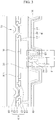
- FIG. 3 is a cross-section view taken along line I-I' of FIG. 2 .
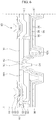
- FIG. 4 is an enlarge view of region P in FIG. 3 .
- the organic light-emitting display device may comprise a lower substrate 110, a thin film transistor 120, a planarization layer 130, a light-emitting structure 140, an auxiliary electrode 150, a first bank insulating layer 161, a second bank insulating layer 162 and a partition wall 170.
- the lower substrate 110 may support the thin film transistor 120 and the light-emitting structure 140.
- the lower substrate 110 may include an insulating material.
- the lower substrate 110 may include a transparent material.
- the lower substrate 110 may include a glass or a plastic.
- a data line DL and a gate line GL intersecting the data line DL may be disposed on the lower substrate 110.
- the thin film transistor 120 may be disposed on a region intersecting the data line DL and the gate line GL.
- the thin film transistor 120 may include a gate electrode 121 disposed close to the lower substrate 110, a gate insulating layer 122 on the gate electrode 121, a semiconductor pattern 123 on the gate insulating layer 122, a source electrode 124 connected to a portion of the semiconductor pattern 123 and a drain electrode 125 connected to an opposite portion of the semiconductor pattern 123.
- the thin film transistor 120 may further include an interlayer insulating layer between the semiconductor pattern 123 and the source/drain electrodes 124 and 125.
- the gate electrode 121, the source electrode 124 and the drain electrode 125 may include a conductive material.
- the gate electrode 121, the source electrode 124 and the drain electrode 125 may include a metal.
- the drain electrode 125 may include a same material as the source electrode 124.
- the gate electrode 121 may include a material different from the source/drain electrodes 124 and 125.
- the gate electrode 121 may be formed with a same material as the gate line GL.
- the data line DL may be formed with a same material as the source/drain electrodes 124 and 125.
- a first power supply line VDD selectively connected to the lower electrode 141 of the light-emitting structure 140 by the thin film transistor 120 may be disposed side by side with the data line DL.
- the first power supply line VDD may include a same material as the source/drain electrodes 124 and 125.
- the gate insulating layer 122 and the interlayer insulating layer may include an insulating material.
- the interlayer insulating layer may include contact holes connecting the source/drain electrodes 124 and 125 to the corresponding portion of the semiconductor pattern 123, respectively.
- the organic light-emitting display device is described that the thin film transistor 120 is in direct contact with the lower substrate 110.
- the organic light-emitting display device according to another embodiment of the present invention may further comprise a buffer layer between the lower substrate 110 and the thin film transistor 120.
- the buffer layer may include an insulating material.
- the buffer layer may be silicon oxide.
- the organic light-emitting display device is described that the thin film transistor 120 includes a semiconductor pattern 123 above the gate electrode 121.
- the organic light-emitting display device may include a thin film transistor 120 which a gate electrode 121 is disposed above a semiconductor pattern 123.
- the planarization layer 130 may be disposed on the thin film transistor 120.
- the planarization layer 130 may remove a thickness difference by the thin film transistor 120.
- the thin film transistor 120 may be completely covered by the planarization layer 130.
- an upper surface of the planarization layer 130 may be parallel with a surface of the lower substrate 110.
- the planarization layer 130 may extend to the outside of the thin film transistor 120.
- the planarization layer 130 may include an insulating material.
- the planarization layer 130 may be silicon oxide.
- the light-emitting structure 140 may generate light realizing a specific color.
- the light-emitting structure 140 may include a lower electrode 141, an organic light-emitting layer 142 and an upper electrode 143, which are sequentially stacked.
- the light-emitting structure 140 may selectively generate light by the thin film transistor 120.
- the lower electrode 141 may be electrically connected to the drain electrode 125 of the thin film transistor 120.
- the light-emitting structure 140 may be disposed on the planarization layer 130.
- the planarization layer 130 may include a contact hole exposing the drain electrode 125 of the thin film transistor 120.
- the lower electrode 141 and the upper electrode 143 may include a conductive material.
- the upper electrode 143 may include a material different from the lower electrode 141.
- the lower electrode 141 may include a high-reflective material, and the upper electrode 143 may include a transparent material.
- the lower electrode 141 may include a metal, and the upper electrode 143 may include ITO or IZO.
- the organic light-emitting display device is described that the lower electrode 141 of the light-emitting structure 140 includes an opaque material.
- the lower electrode 141 may include a transparent material.
- the organic light-emitting display device may be bottom emission type.
- the organic light-emitting layer 142 may generate light, the brightness of which corresponds to the voltage difference between the lower electrode 141 and the upper electrode 143.
- the light generated by the organic light-emitting layer 142 may realize a specific color.
- the light generated by the organic light-emitting layer 142 may realize white, blue, green or red.
- the organic light-emitting layer 142 may include an emitting material layer (EML) having an organic emitting material.
- EML emitting material layer
- the organic light-emitting layer 142 may be a multi-layer structure, in order to increase luminous efficacy.
- the organic light-emitting layer 142 may further include a hole injection layer (HIL), a hole transporting layer (HTL), an electron transporting layer (ETL), and an electron injection layer (EIL).
- HIL hole injection layer
- HTL hole transporting layer
- ETL electron transporting layer
- EIL electron injection layer
- the auxiliary electrode 150 may supply a second power to the upper electrode 143 of the light-emitting structure 140.
- the auxiliary electrode 150 may be connected to a second power supply line VSS.
- the auxiliary electrode 150 may be a portion of the second power supply line VSS.
- the auxiliary electrode 150 may be disposed on the planarization layer 130.
- the auxiliary electrode 150 may be disposed between the lower electrodes 141 of the adjacent light-emitting structures 140.
- the auxiliary electrode 150 may be disposed side by side with the lower electrode 141.
- the auxiliary electrode 150 may include a conductive material.
- the auxiliary electrode 150 may include a same material as the lower electrode 141 of the light-emitting structure 140.
- the auxiliary electrode 150 may include a metal.
- the first bank insulating layer 161 may cover an edge of the lower electrode 141 of the light-emitting structure 140.
- the first bank insulating layer 161 may include a first hole 161h partially exposing an upper surface of the lower electrode 141.
- the organic light-emitting layer 142 and the upper electrode 143 may be sacked on a portion of an upper surface of the lower electrode 141 which is exposed by the first bank insulating layer 161.
- the organic light-emitting layer 142 and the upper electrode 143 may extend onto the first bank insulating layer 161.
- the first bank insulating layer 161 may include an insulating material.
- the first bank insulating layer 161 may include an organic material, such as benzocyclobutene (BCB), poly-imide and photo-acryl.
- the first bank insulating layer 161 may be disposed on the auxiliary electrode 150.
- the first bank insulating layer 161 may include a second hole 162h partially exposing an upper surface of the auxiliary electrode 150.
- the second hole 162h may be disposed between the adjacent lower electrodes 141.
- the second bank insulating layer 162 may be disposed at the inside of the second hole 162h of the first bank insulating layer 161.
- a horizontal area of the second bank insulating layer 162 may be smaller than a horizontal area of the second hole 162h of the first bank insulating layer 161.
- the second bank insulating layer 162 may be spaced apart from the first bank insulating layer 161. All side surfaces of the second bank insulating layer 162 may be not in contact with the first bank insulating layer 161.
- the second bank insulating layer 162 may be isolated at the inside of the second hole 162h of the first bank insulating layer 161.
- All side surfaces of the second bank insulating layer 162 may be positively tapered.
- the side surfaces of the first bank insulating layer 161 facing the second bank insulating layer 162 may be positively tapered.
- the horizontal area of the second hole 162h may be increased away from the auxiliary electrode 150.
- the organic light-emitting layer 142 and the upper electrode 143 may extend onto the side surfaces of the first bank insulating layer 161 facing the second bank insulating layer 162.
- the upper electrode 143 may be connected to the auxiliary electrode 150 through the second hole 162h.
- the side surfaces of the first bank insulating layer 161 facing the second bank insulating layer 162 may be completely covered by the upper electrode 143.
- the second bank insulating layer 162 may be a bar shape extending in a direction within the second hole 162h.
- the second hole 162h may extend in a direction perpendicular to the direction in which the auxiliary electrode 150 extends.
- a length of the second hole 162h in a widthwise direction of the auxiliary electrode 150 may be larger than the width of the auxiliary electrode 150.
- the second bank insulating layer may be a bar shape intersecting the auxiliary electrode 150.
- the second bank insulating layer 162 may be disposed on a same layer as the first bank insulating layer 161.
- the second bank insulating layer 162 may include an insulating material.
- the second bank insulating layer 162 may include a same material as the first bank insulating layer 161.
- the second bank insulating layer 162 may include an organic material, such as benzocyclobutene (BCB), poly-imide and photo-acryl.
- the partition wall 170 may be disposed on the second bank insulating layer 162.
- the partition wall 170 may partially cut off the organic light-emitting layer 142 such that a contact area between the upper electrode 143 and the auxiliary electrode 150 may be sufficiently ensured.
- a side surface of the partition wall 170 may be negatively tapered.
- the organic light-emitting layer 142 may be not formed and/or deposited under the negatively tapered side surface of the partition wall 170.
- the upper electrode 143 may be connected to the auxiliary electrode 150 under the negatively tapered side surface of the partition wall 170.
- the upper electrode 143 may be not deposited and/or formed on at least a part of the side surface of the second bank insulating layer 162 by the partition wall 170.
- the maximum horizontal area of the partition wall 170 may be larger than the horizontal area of the second bank insulating layer 162.
- the second bank insulating layer 162 may completely overlap the partition wall 170.
- the maximum horizontal area of the partition wall 170 may be smaller than the horizontal area of the second hole 162h.
- the outermost side surface of the partition wall 170 may be disposed between the first bank insulating layer 161 and the second bank insulating layer 162.
- the partition wall 170 may include an insulating material.
- the second bank insulating layer 162 supporting the partition wall 170 may be completely isolated from the first bank insulating layer 161 covering an edge of the lower electrode 141 of the light-emitting structure 140.
- the moisture permeated through the side surface of the second bank insulating layer 162 which is exposed to the outside by the partition wall 170 may be not move to the light-emitting structure 140. Therefore, in the organic light-emitting display device according to the embodiment of the present invention, the degradation of the organic light-emitting layer 142 by the permeated moisture may be prevented.
- all side surfaces of the first bank insulating layer 161 facing the second bank insulating layer 162 may be positively tapered.
- all side surfaces of the first bank insulating layer 161 facing the second bank insulating layer 162 may be covered by the upper electrode 143. Therefore, in the organic light-emitting display device according to the embodiment of the present invention, the degradation of the organic light-emitting layer 142 by the permeated moisture may be further prevented.
- the organic light-emitting display device may further comprise a protective layer 180 in order to prevent the damage of the upper electrode 143.
- the protective layer 180 may include an inorganic material and/or an organic material in order to delay and/or prevent the permeation of the moisture.
- the protective layer 180 may be a structure in which the inorganic material and the organic material are stacked.
- the protective layer 180 may extend along the upper electrode 143.
- the protective layer 180 may extend onto the side surfaces of the first bank insulating layer 161 facing the second bank insulating layer 162.
- the side surfaces of the first bank insulating layer 161 facing the second bank insulating layer 162 may be completely covered by the upper electrode 143 and the protective layer 180. Therefore, in the organic light-emitting display device according to the embodiment of the present invention, the degradation of the organic light-emitting layer 142 by the permeation of the moisture may be efficiently prevented.
- the organic light-emitting display device is described that the second hole 162h of the first bank insulating layer 161 extends in a direction perpendicular to the direction in which the auxiliary electrode extends.
- the second hole 162h of the first bank insulating layer 161 may extend in a direction parallel with the direction in which the auxiliary electrode extends, as shown in FIG. 5 .
- a width of the second hole 162h may be larger than the width of the auxiliary electrode 150.
- An edge of the auxiliary electrode 150 may be exposed by the second hole 162h.
- the auxiliary electrode 150 includes a same material as the lower electrode 141, and the auxiliary electrode 150 is disposed on a same layer as the lower electrode 141.
- the auxiliary electrode 150 may include a same material as the source/drain electrodes 124 and 125, and the auxiliary electrode 150 may be disposed on a same layer as the source/drain electrodes 124 and 125, as shown in FIG. 6 .
- the organic light-emitting display device may further comprise a first passivation layer 210 between the thin film transistor 120 and the planarization layer 130.
- the second hole 162h of the first bank insulating layer 161 may partially expose the upper surface of the auxiliary electrode 250 by penetrating the planarization layer 130 and the first passivation layer 210.
- a second passivation layer 220 and the second bank insulating layer 162 stacked to have an under-cut may be disposed on the auxiliary electrode 250.
- the under-cut by the second passivation layer 220 and the second bank insulating layer 162 may connect the upper electrode 143 of the light-emitting structure 140 to the auxiliary electrode 250.
- the second passivation layer 220 and the second bank insulating layer 162 may be not in contact with the first passivation layer 210, the planarization layer 130 and the first bank insulating layer 161 within the second hole 162.
- the side surface of the first passivation layer 210, the side surface of the planarization layer 130 and the side surface of the first bank insulating layer 161 which face the second passivation layer 220 and the second bank insulating layer 162 may be positively tapered.
- the upper electrode 143 may extend onto the side surface of the first passivation layer 210, the side surface of the planarization layer 130 and the side surface of the first bank insulating layer 161.
- the organic light-emitting display device may include an insulating structure which supports a partition wall and is isolated from another insulating structure disposed side by side with the insulating structure.
- the organic light-emitting display device may prevent that the external moisture permeates to an organic light-emitting layer through the insulating structure supporting the partition wall. Therefore, in the organic light-emitting display device according to the embodiments of the present invention, a contact area between an upper electrode and an auxiliary electrode may be sufficiently ensured by the partition wall, and the degradation of a light-emitting layer by the moisture permeated from the outside may be prevented.
Landscapes
- Physics & Mathematics (AREA)
- Optics & Photonics (AREA)
- Engineering & Computer Science (AREA)
- Microelectronics & Electronic Packaging (AREA)
- Manufacturing & Machinery (AREA)
- Electroluminescent Light Sources (AREA)
Abstract
Description
- The present invention relates to an organic light-emitting display device connecting an auxiliary electrode to an upper electrode using a partition wall.
- Generally, electronic appliances, such as a monitor, a TV, a laptop computer, and a digital camera, include a display device to realize an image. For example, the display device may include a liquid crystal display device and an organic light-emitting display device.
- The organic light-emitting display device may include light-emitting structure. For example, the light-emitting structure may include a lower electrode, a light-emitting layer and an upper electrode, which are sequentially stacked. In the organic light-emitting display device, an auxiliary electrode is used in order to prevent voltage drop and transport power supplying through the upper electrode.
- The organic light-emitting display device may prevent the deposition of the organic light-emitting layer on an upper surface of the auxiliary electrode using a partition wall, in order to prevent that the auxiliary electrode does not enough contact with the upper electrode by the organic light-emitting layer between the lower electrode and the upper electrode.
- However, since the upper electrode and/or a protective layer formed on the upper electrode may be not deposited on an insulating layer, such as a bank insulating layer supporting the partition wall by the partition wall, the path of permeating the external moisture to the organic light-emitting layer may be provided.
- Accordingly, the present invention is directed to an organic light-emitting display device having a partition wall that substantially obviates one or more problems due to limitations and disadvantages of the related art.
- One object of the present invention is to provide an organic light-emitting display device which may prevent that the moisture is permeated through the insulating layer supporting the partition wall.
- Another object of the present invention is to provide an organic light-emitting display device which may enough ensure a contact area between an upper electrode and an auxiliary electrode using a partition wall, and may prevent that a degradation of an organic light-emitting layer by the moisture permeated from the outside.
- Additional advantages, objects, and features of the invention will be set forth in part in the description which follows and in part will become apparent to those having ordinary skill in the art upon examination of the following or may be learned from practice of the invention. The objectives and other advantages of the invention may be realized and attained by the structure particularly pointed out in the written description and claims hereof as well as the appended drawings.
- To achieve these objects and other advantages and in accordance with the purpose of the invention, as embodied and broadly described herein, there is provided an organic light-emitting display device including an auxiliary electrode spaced apart from a lower electrode. The auxiliary electrode may be disposed side by side with the lower electrode. It may be said that "side by side" entails the components being present on the same layer. A first bank insulating layer may be disposed on the lower electrode and the auxiliary electrode. The first bank insulating layer includes a first hole exposing an upper surface of the lower electrode and a second hole partially exposing an upper surface of the auxiliary electrode. It may be said that the first bank insulating layer includes a first hole such that at least a portion of an upper surface of the lower electrode is not covered by the first bank insulating layer and a second hole such that at least a portion of an upper surface of the auxiliary electrode is not covered by the second bank insulating layer. A second bank insulating layer is disposed at the inside of the second hole. The second bank insulating layer is spaced apart from the first bank insulating layer. A partition wall overlaps the second bank insulating layer. In other words, the partition wall is on the second bank insulating layer and overhangs the second bank insulating layer. In overhanging the second bank insulating layer, the partition wall's boundary extends beyond the boundary of the second bank insulating layer where the partition wall and the second bank insulating layer meet.
- Side surfaces of the first bank insulating layer facing the second bank insulating layer may be positively tapered. It may be said that "positively tapered" refers to a surface being inclined so as to reduce the horizontal area of the component with increasing distance from the component that it is described as being on. This is in contrast to "negatively tapered", which may be said to refer to the surface being inclined so as to increase the horizontal area of the component with increasing distance from the component that it is described as being on. The horizontal area is the area perpendicular to the general stacking direction of the layers.
- An organic light-emitting layer and an upper electrode may be sequentially stacked on a portion the lower electrode exposed by the first hole. In other words, the organic light-emitting layer is stacked on a portion of the lower electrode and the upper electrode is stacked on the organic light-emitting layer. The upper electrode may extend onto the side surfaces of the first bank insulating layer facing the second bank insulating layer. The upper electrode may be connected to the auxiliary electrode through the second hole, i.e. the upper electrode is directly connected to the auxiliary electrode.
- The side surfaces of the first bank insulating layer facing the second bank insulating layer may be completely covered by the upper electrode.
- A protective layer may be disposed on the upper electrode. The protective layer may extend along the upper electrode.
- The auxiliary electrode may include a same material as the lower electrode. The second bank insulating layer may include a same material as the first bank insulating layer.
- The maximum horizontal area of the partition wall may be larger than a horizontal area of the second bank insulating layer. The maximum horizontal area of the partition wall may be smaller than a horizontal area of the first hole.
- The outermost side surface of the partition wall may be disposed between the first bank insulating layer and the second bank insulating layer. In other words, an outermost point of a side surface of the partition wall is disposed over a point between the first bank insulating layer and the second bank insulating layer. The term "over" is used in reference to the general stacking direction of the layers.
- The second bank insulating layer may extend in a direction perpendicular to the direction in which the auxiliary electrode extends at the inside of the second hole. It may be said that a base of the second bank insulating layer extends in a direction perpendicular to the direction in which the auxiliary electrode extends. The base of the second bank insulating layer is the surface that is in contact with the component on which the second bank insulating layer is on.
- A length of the second bank insulating layer in a widthwise direction of the auxiliary electrode may be larger than the width of the auxiliary electrode.
- Also provided is an organic light-emitting display device comprising an auxiliary electrode spaced apart from a lower electrode. A first insulating layer may be on the lower electrode and the auxiliary electrode. The first insulating layer including a first hole partially exposing the lower electrode and a second hole partially exposing the auxiliary electrode. It may be said that the first bank insulating layer includes a first hole such that the lower electrode is not covered by the first bank insulating layer and a second hole such that the auxiliary electrode is not covered by the second bank insulating layer. An insulation structure is provided at the inside of the second hole of the first insulating layer, and an under-cut is disposed at an edge of the insulating structure, wherein a side surface of the first insulating layer facing the insulation structure is positively tapered. The under-cut is a region of the insulating structure where a portion of the insulating structure overhangs a lower portion of the insulating structure.
- The accompanying drawings, which are included to provide a further understanding of the invention and are incorporated in and constitute a part of this application, illustrate embodiment(s) of the invention and together with the description serve to explain the principle of the invention. In the drawings:
-
FIG. 1 is a top view schematically showing an organic light-emitting display device according to an embodiment of the present invention; -
FIG. 2 is an enlarge view of region R inFIG. 1 ; -
FIG. 3 is a cross-section view taken along line I-I' ofFIG. 2 ; -
FIG. 4 is an enlarge view of region P inFIG. 3 ; -
FIGS. 5 and6 are views respectively showing various examples of an organic light-emitting display device according to another embodiment of the present invention; - Hereinafter, details related to the above objects, technical configurations, and operational effects of the embodiments of the present invention will be clearly understood by the following detailed description with reference to the drawings, which illustrate some embodiments of the present invention. Here, the embodiments of the present invention are provided in order to allow the technical sprit of the present invention to be satisfactorily transferred to those skilled in the art, and thus the present invention may be embodied in other forms and is not limited to the embodiments described below.
- In addition, the same or extremely similar elements may be designated by the same reference numerals throughout the specification, and in the drawings, the lengths and thickness of layers and regions may be exaggerated for convenience. It will be understood that, when a first element is referred to as being "on" a second element, although the first element may be disposed on the second element so as to come into contact with the second element, a third element may be interposed between the first element and the second element.
- Here, terms such as, for example, "first" and "second" may be used to distinguish any one element with another element. However, the first element and the second element may be arbitrary named according to the convenience of those skilled in the art without departing the technical sprit of the present invention.
- The terms used in the specification of the present invention are merely used in order to describe particular embodiments, and are not intended to limit the scope of the present invention. For example, an element described in the singular form is intended to include a plurality of elements unless the context clearly indicates otherwise. In addition, in the specification of the present invention, it will be further understood that the terms "comprises" and "includes" specify the presence of stated features, integers, steps, operations, elements, components, and/or combinations thereof, but do not preclude the presence or addition of one or more other features, integers, steps, operations, elements, components, and/or combinations.
- Unless otherwise defined, all terms (including technical and scientific terms) used herein have the same meaning as commonly understood by one of ordinary skill in the art to which example embodiments belong. It will be further understood that terms, such as those defined in commonly used dictionaries, should be interpreted as having a meaning that is consistent with their meaning in the context of the relevant art and should not be interpreted in an idealized or overly formal sense unless expressly so defined herein.
-
FIG. 1 is a top view schematically showing a display device according to an embodiment of the present invention.FIG. 2 is an enlarge view of region R inFIG. 1 .FIG. 3 is a cross-section view taken along line I-I' ofFIG. 2 .FIG. 4 is an enlarge view of region P inFIG. 3 . - Referring to
FIGS. 1 to 4 , the organic light-emitting display device according to the embodiment of the present invention may comprise alower substrate 110, athin film transistor 120, aplanarization layer 130, a light-emittingstructure 140, anauxiliary electrode 150, a firstbank insulating layer 161, a secondbank insulating layer 162 and apartition wall 170. - The
lower substrate 110 may support thethin film transistor 120 and the light-emittingstructure 140. Thelower substrate 110 may include an insulating material. Thelower substrate 110 may include a transparent material. For example, thelower substrate 110 may include a glass or a plastic. - A data line DL and a gate line GL intersecting the data line DL may be disposed on the
lower substrate 110. Thethin film transistor 120 may be disposed on a region intersecting the data line DL and the gate line GL. Thethin film transistor 120 may include agate electrode 121 disposed close to thelower substrate 110, agate insulating layer 122 on thegate electrode 121, asemiconductor pattern 123 on thegate insulating layer 122, asource electrode 124 connected to a portion of thesemiconductor pattern 123 and adrain electrode 125 connected to an opposite portion of thesemiconductor pattern 123. Thethin film transistor 120 may further include an interlayer insulating layer between thesemiconductor pattern 123 and the source/drain electrodes - The
gate electrode 121, thesource electrode 124 and thedrain electrode 125 may include a conductive material. For example, thegate electrode 121, thesource electrode 124 and thedrain electrode 125 may include a metal. Thedrain electrode 125 may include a same material as thesource electrode 124. Thegate electrode 121 may include a material different from the source/drain electrodes - The
gate electrode 121 may be formed with a same material as the gate line GL. The data line DL may be formed with a same material as the source/drain electrodes lower electrode 141 of the light-emittingstructure 140 by thethin film transistor 120 may be disposed side by side with the data line DL. The first power supply line VDD may include a same material as the source/drain electrodes - The
gate insulating layer 122 and the interlayer insulating layer may include an insulating material. The interlayer insulating layer may include contact holes connecting the source/drain electrodes semiconductor pattern 123, respectively. - The organic light-emitting display device according to the embodiment of the present invention is described that the
thin film transistor 120 is in direct contact with thelower substrate 110. However, the organic light-emitting display device according to another embodiment of the present invention may further comprise a buffer layer between thelower substrate 110 and thethin film transistor 120. The buffer layer may include an insulating material. For example, the buffer layer may be silicon oxide. - The organic light-emitting display device according to the embodiment of the present invention is described that the
thin film transistor 120 includes asemiconductor pattern 123 above thegate electrode 121. However, the organic light-emitting display device according to another embodiment of the present invention may include athin film transistor 120 which agate electrode 121 is disposed above asemiconductor pattern 123. - The
planarization layer 130 may be disposed on thethin film transistor 120. Theplanarization layer 130 may remove a thickness difference by thethin film transistor 120. Thethin film transistor 120 may be completely covered by theplanarization layer 130. For example, an upper surface of theplanarization layer 130 may be parallel with a surface of thelower substrate 110. Theplanarization layer 130 may extend to the outside of thethin film transistor 120. - The
planarization layer 130 may include an insulating material. For example, theplanarization layer 130 may be silicon oxide. - The light-emitting
structure 140 may generate light realizing a specific color. For example, the light-emittingstructure 140 may include alower electrode 141, an organic light-emittinglayer 142 and anupper electrode 143, which are sequentially stacked. - The light-emitting
structure 140 may selectively generate light by thethin film transistor 120. For example, thelower electrode 141 may be electrically connected to thedrain electrode 125 of thethin film transistor 120. The light-emittingstructure 140 may be disposed on theplanarization layer 130. Theplanarization layer 130 may include a contact hole exposing thedrain electrode 125 of thethin film transistor 120. - The
lower electrode 141 and theupper electrode 143 may include a conductive material. Theupper electrode 143 may include a material different from thelower electrode 141. For example, thelower electrode 141 may include a high-reflective material, and theupper electrode 143 may include a transparent material. For example, thelower electrode 141 may include a metal, and theupper electrode 143 may include ITO or IZO. - The organic light-emitting display device according to the embodiment of the present invention is described that the
lower electrode 141 of the light-emittingstructure 140 includes an opaque material. However, in the organic light-emitting display device according to another embodiment of the present invention, thelower electrode 141 may include a transparent material. For example, the organic light-emitting display device according to another embodiment of the present invention may be bottom emission type. - The organic light-emitting
layer 142 may generate light, the brightness of which corresponds to the voltage difference between thelower electrode 141 and theupper electrode 143. The light generated by the organic light-emittinglayer 142 may realize a specific color. For example, the light generated by the organic light-emittinglayer 142 may realize white, blue, green or red. - The organic light-emitting
layer 142 may include an emitting material layer (EML) having an organic emitting material. The organic light-emittinglayer 142 may be a multi-layer structure, in order to increase luminous efficacy. For example, the organic light-emittinglayer 142 may further include a hole injection layer (HIL), a hole transporting layer (HTL), an electron transporting layer (ETL), and an electron injection layer (EIL). - The
auxiliary electrode 150 may supply a second power to theupper electrode 143 of the light-emittingstructure 140. Theauxiliary electrode 150 may be connected to a second power supply line VSS. For example, theauxiliary electrode 150 may be a portion of the second power supply line VSS. - The
auxiliary electrode 150 may be disposed on theplanarization layer 130. Theauxiliary electrode 150 may be disposed between thelower electrodes 141 of the adjacent light-emittingstructures 140. For example, theauxiliary electrode 150 may be disposed side by side with thelower electrode 141. - The
auxiliary electrode 150 may include a conductive material. Theauxiliary electrode 150 may include a same material as thelower electrode 141 of the light-emittingstructure 140. For example, theauxiliary electrode 150 may include a metal. - The first
bank insulating layer 161 may cover an edge of thelower electrode 141 of the light-emittingstructure 140. The firstbank insulating layer 161 may include afirst hole 161h partially exposing an upper surface of thelower electrode 141. The organic light-emittinglayer 142 and theupper electrode 143 may be sacked on a portion of an upper surface of thelower electrode 141 which is exposed by the firstbank insulating layer 161. The organic light-emittinglayer 142 and theupper electrode 143 may extend onto the firstbank insulating layer 161. - The first
bank insulating layer 161 may include an insulating material. For example, the firstbank insulating layer 161 may include an organic material, such as benzocyclobutene (BCB), poly-imide and photo-acryl. - The first
bank insulating layer 161 may be disposed on theauxiliary electrode 150. The firstbank insulating layer 161 may include asecond hole 162h partially exposing an upper surface of theauxiliary electrode 150. For example, thesecond hole 162h may be disposed between the adjacentlower electrodes 141. - The second
bank insulating layer 162 may be disposed at the inside of thesecond hole 162h of the firstbank insulating layer 161. A horizontal area of the secondbank insulating layer 162 may be smaller than a horizontal area of thesecond hole 162h of the firstbank insulating layer 161. The secondbank insulating layer 162 may be spaced apart from the firstbank insulating layer 161. All side surfaces of the secondbank insulating layer 162 may be not in contact with the firstbank insulating layer 161. For example, the secondbank insulating layer 162 may be isolated at the inside of thesecond hole 162h of the firstbank insulating layer 161. - All side surfaces of the second
bank insulating layer 162 may be positively tapered. The side surfaces of the firstbank insulating layer 161 facing the secondbank insulating layer 162 may be positively tapered. The horizontal area of thesecond hole 162h may be increased away from theauxiliary electrode 150. - The organic light-emitting
layer 142 and theupper electrode 143 may extend onto the side surfaces of the firstbank insulating layer 161 facing the secondbank insulating layer 162. Theupper electrode 143 may be connected to theauxiliary electrode 150 through thesecond hole 162h. For example, the side surfaces of the firstbank insulating layer 161 facing the secondbank insulating layer 162 may be completely covered by theupper electrode 143. - The second
bank insulating layer 162 may be a bar shape extending in a direction within thesecond hole 162h. Thesecond hole 162h may extend in a direction perpendicular to the direction in which theauxiliary electrode 150 extends. A length of thesecond hole 162h in a widthwise direction of theauxiliary electrode 150 may be larger than the width of theauxiliary electrode 150. The second bank insulating layer may be a bar shape intersecting theauxiliary electrode 150. - The second
bank insulating layer 162 may be disposed on a same layer as the firstbank insulating layer 161. The secondbank insulating layer 162 may include an insulating material. The secondbank insulating layer 162 may include a same material as the firstbank insulating layer 161. For example, the secondbank insulating layer 162 may include an organic material, such as benzocyclobutene (BCB), poly-imide and photo-acryl. - The
partition wall 170 may be disposed on the secondbank insulating layer 162. Thepartition wall 170 may partially cut off the organic light-emittinglayer 142 such that a contact area between theupper electrode 143 and theauxiliary electrode 150 may be sufficiently ensured. For example, a side surface of thepartition wall 170 may be negatively tapered. The organic light-emittinglayer 142 may be not formed and/or deposited under the negatively tapered side surface of thepartition wall 170. Theupper electrode 143 may be connected to theauxiliary electrode 150 under the negatively tapered side surface of thepartition wall 170. Theupper electrode 143 may be not deposited and/or formed on at least a part of the side surface of the secondbank insulating layer 162 by thepartition wall 170. - The maximum horizontal area of the
partition wall 170 may be larger than the horizontal area of the secondbank insulating layer 162. For example, the secondbank insulating layer 162 may completely overlap thepartition wall 170. The maximum horizontal area of thepartition wall 170 may be smaller than the horizontal area of thesecond hole 162h. For example, the outermost side surface of thepartition wall 170 may be disposed between the firstbank insulating layer 161 and the secondbank insulating layer 162. Thepartition wall 170 may include an insulating material. - In the organic light-emitting display device according to the embodiment of the present invention, the second
bank insulating layer 162 supporting thepartition wall 170 may be completely isolated from the firstbank insulating layer 161 covering an edge of thelower electrode 141 of the light-emittingstructure 140. Thus, in the organic light-emitting display device according to the embodiment of the present invention, the moisture permeated through the side surface of the secondbank insulating layer 162 which is exposed to the outside by thepartition wall 170 may be not move to the light-emittingstructure 140. Therefore, in the organic light-emitting display device according to the embodiment of the present invention, the degradation of the organic light-emittinglayer 142 by the permeated moisture may be prevented. - Also, in the organic light-emitting display device according to the embodiment of the present invention, all side surfaces of the first
bank insulating layer 161 facing the secondbank insulating layer 162 may be positively tapered. Thus, in the organic light-emitting display device according to the embodiment of the present invention, all side surfaces of the firstbank insulating layer 161 facing the secondbank insulating layer 162 may be covered by theupper electrode 143. Therefore, in the organic light-emitting display device according to the embodiment of the present invention, the degradation of the organic light-emittinglayer 142 by the permeated moisture may be further prevented. - The organic light-emitting display device according to the embodiment of the present invention may further comprise a
protective layer 180 in order to prevent the damage of theupper electrode 143. Theprotective layer 180 may include an inorganic material and/or an organic material in order to delay and/or prevent the permeation of the moisture. For example, theprotective layer 180 may be a structure in which the inorganic material and the organic material are stacked. - The
protective layer 180 may extend along theupper electrode 143. For example, theprotective layer 180 may extend onto the side surfaces of the firstbank insulating layer 161 facing the secondbank insulating layer 162. Thus, in the organic light-emitting display device according to the embodiment of the present invention, the side surfaces of the firstbank insulating layer 161 facing the secondbank insulating layer 162 may be completely covered by theupper electrode 143 and theprotective layer 180. Therefore, in the organic light-emitting display device according to the embodiment of the present invention, the degradation of the organic light-emittinglayer 142 by the permeation of the moisture may be efficiently prevented. - The organic light-emitting display device according to the embodiment of the present invention is described that the
second hole 162h of the firstbank insulating layer 161 extends in a direction perpendicular to the direction in which the auxiliary electrode extends. However, in the organic light-emitting display device according to another embodiment of the present invention, thesecond hole 162h of the firstbank insulating layer 161 may extend in a direction parallel with the direction in which the auxiliary electrode extends, as shown inFIG. 5 . A width of thesecond hole 162h may be larger than the width of theauxiliary electrode 150. An edge of theauxiliary electrode 150 may be exposed by thesecond hole 162h. - The organic light-emitting display device according to the embodiment of the present invention is described that the
auxiliary electrode 150 includes a same material as thelower electrode 141, and theauxiliary electrode 150 is disposed on a same layer as thelower electrode 141. However, in the organic light-emitting display device according to another embodiment of the present invention, theauxiliary electrode 150 may include a same material as the source/drain electrodes auxiliary electrode 150 may be disposed on a same layer as the source/drain electrodes FIG. 6 . - The organic light-emitting display device according to another embodiment of the present invention may further comprise a
first passivation layer 210 between thethin film transistor 120 and theplanarization layer 130. Thesecond hole 162h of the firstbank insulating layer 161 may partially expose the upper surface of theauxiliary electrode 250 by penetrating theplanarization layer 130 and thefirst passivation layer 210. - In the organic light-emitting display device according to another embodiment of the present invention, a
second passivation layer 220 and the secondbank insulating layer 162 stacked to have an under-cut may be disposed on theauxiliary electrode 250. The under-cut by thesecond passivation layer 220 and the secondbank insulating layer 162 may connect theupper electrode 143 of the light-emittingstructure 140 to theauxiliary electrode 250. - In the organic light-emitting display device according to another embodiment of the present invention, the
second passivation layer 220 and the secondbank insulating layer 162 may be not in contact with thefirst passivation layer 210, theplanarization layer 130 and the firstbank insulating layer 161 within thesecond hole 162. The side surface of thefirst passivation layer 210, the side surface of theplanarization layer 130 and the side surface of the firstbank insulating layer 161 which face thesecond passivation layer 220 and the secondbank insulating layer 162 may be positively tapered. Theupper electrode 143 may extend onto the side surface of thefirst passivation layer 210, the side surface of theplanarization layer 130 and the side surface of the firstbank insulating layer 161. Thus, in the organic light-emitting display device according to another embodiment of the present invention, the degradation of the organic light-emittinglayer 142 by the moisture permeated from the outside may be efficiently prevented. - In the result, the organic light-emitting display device according to the embodiments of the present invention may include an insulating structure which supports a partition wall and is isolated from another insulating structure disposed side by side with the insulating structure. Thus, the organic light-emitting display device according to the embodiments of the present invention may prevent that the external moisture permeates to an organic light-emitting layer through the insulating structure supporting the partition wall. Therefore, in the organic light-emitting display device according to the embodiments of the present invention, a contact area between an upper electrode and an auxiliary electrode may be sufficiently ensured by the partition wall, and the degradation of a light-emitting layer by the moisture permeated from the outside may be prevented.
- The following list of embodiments forms part of the description.
- 1. An organic light-emitting display device comprising:
- an auxiliary electrode disposed side by side with a lower electrode;
- a first bank insulating layer on the lower electrode and the auxiliary electrode, the first bank insulating layer including a first hole exposing an upper surface of the lower electrode and a second hole partially exposing an upper surface of the auxiliary electrode;
- a second bank insulating layer at the inside of the second hole of the first bank insulating layer, the second bank insulating layer spaced apart from the first bank insulating layer; and
- a partition wall overlapping with the second bank insulating layer.
- 2. The organic light-emitting display device according to embodiment 1, wherein side surfaces of the first bank insulating layer facing the second bank insulating layer are positively tapered.
- 3. The organic light-emitting display device according to embodiment 1, further comprising an organic light-emitting layer and an upper electrode which are sequentially stacked on a portion of the lower electrode which is exposed by the first hole,
wherein the upper electrode extends onto side surfaces of the first bank insulating layer facing the second bank insulating layer. - 4. The organic light-emitting display device according to embodiment 3, wherein the side surfaces of the first bank insulating layer facing the second bank insulating layer are completely covered by the upper electrode.
- 5. The organic light-emitting display device according to embodiment 3, further comprising a protective layer on the upper electrode, the protective layer extending along the upper electrode.
- 6. The organic light-emitting display device according to embodiment 1, wherein the auxiliary electrode includes a same material as the lower electrode, and the second bank insulating layer includes a same material as the first bank insulating layer.
- 7. The organic light-emitting display device according to embodiment 1, wherein the maximum horizontal area of the partition wall is larger than a horizontal area of the second bank insulating layer, and is smaller than a horizontal area of the first hole.
- 8. The organic light-emitting display device according to embodiment 7, wherein an outermost side surface of the partition wall is disposed between the first bank insulating layer and the second bank insulating layer.
- 9. The organic light-emitting display device according to embodiment 1, wherein the second bank insulating layer extends in a direction perpendicular to the direction in which the auxiliary electrode extends at the inside of the second hole.
- 10. The organic light-emitting display device according to embodiment 9, wherein a length of the second bank insulating layer in a widthwise direction of the auxiliary electrode is larger than the width of the auxiliary electrode.
- 11. An organic light-emitting display device comprising:
- an auxiliary electrode spaced apart from a lower electrode;
- a first insulating layer on the lower electrode and the auxiliary electrode, the first insulating layer including a first hole partially exposing the lower electrode and a second hole partially exposing the auxiliary electrode; and
- an insulation structure at the inside of the second hole of the first insulating layer, an under-cut disposed at an edge of the insulating structure,
- wherein a side surface of the first insulating layer facing the insulation structure is positively tapered.
- 12. The organic light-emitting display device according to embodiment 11, wherein the auxiliary electrode includes a material different from the lower electrode.
Claims (13)
- An organic light-emitting display device comprising:an auxiliary electrode spaced apart from a lower electrode;a first bank insulating layer, the first bank insulating layer including a first hole such that at least a portion of an upper surface of the lower electrode is not covered by the first bank insulating layer and a second hole such that at least a portion of an upper surface of the auxiliary electrode is not covered by the second bank insulating layer;a second bank insulating layer inside the second hole of the first bank insulating layer, the second bank insulating layer spaced apart from the first bank insulating layer; anda partition wall on the second bank insulating layer, wherein the partition wall overhangs the second bank insulating layer.
- The organic light-emitting display device of claim 1, wherein the lower electrode is disposed side by side with the auxiliary electrode.
- The organic light-emitting display device according to claim 1 or claim 2, wherein side surfaces of the first bank insulating layer facing the second bank insulating layer are positively tapered.
- The organic light-emitting display device according to any preceding claim, further comprising an organic light-emitting layer and an upper electrode which are sequentially stacked on a portion of the lower electrode which is exposed by the first hole,
wherein the upper electrode extends onto side surfaces of the first bank insulating layer facing the second bank insulating layer. - The organic light-emitting display device according to claim 4, wherein the side surfaces of the first bank insulating layer facing the second bank insulating layer are completely covered by the upper electrode.
- The organic light-emitting display device according to claim 4 or claim 5, further comprising a protective layer on the upper electrode, the protective layer extending along the upper electrode.
- The organic light-emitting display device according to any preceding claim, wherein the auxiliary electrode includes a same material as the lower electrode, and the second bank insulating layer includes a same material as the first bank insulating layer.
- The organic light-emitting display device according to any preceding claim, wherein the maximum horizontal area of the partition wall is larger than a horizontal area of the second bank insulating layer, and is smaller than a horizontal area of the first hole.
- The organic light-emitting display device according to any preceding claim, wherein an outermost point of a side surface of the partition wall is disposed over a point between the first bank insulating layer and the second bank insulating layer.
- The organic light-emitting display device according to any preceding claim, wherein a base of the second bank insulating layer extends in a direction perpendicular to the direction in which the auxiliary electrode extends.
- The organic light-emitting display device according to claim 10, wherein a length of the second bank insulating layer in a widthwise direction of the auxiliary electrode is larger than the width of the auxiliary electrode.
- An organic light-emitting display device comprising:an auxiliary electrode spaced apart from a lower electrode;a first insulating layer, the first insulating layer including a first hole such that at least a portion of the lower electrode is not covered by the first insulating layer and a second hole such that at least a portion of the auxiliary electrode is not covered by the first insulating layer; andan insulation structure inside the second hole of the first insulating layer, wherein the insulation structure comprises an under-cut disposed at an edge of the insulating structure,wherein a side surface of the first insulating layer facing the insulation structure is positively tapered.
- The organic light-emitting display device according to any preceding claim, wherein the auxiliary electrode includes a material different from the lower electrode.
Applications Claiming Priority (1)
| Application Number | Priority Date | Filing Date | Title |
|---|---|---|---|
| KR1020160112196A KR102612040B1 (en) | 2016-08-31 | 2016-08-31 | Organic Light Emitting Display device having a partition wall |
Publications (2)
| Publication Number | Publication Date |
|---|---|
| EP3291301A1 true EP3291301A1 (en) | 2018-03-07 |
| EP3291301B1 EP3291301B1 (en) | 2020-09-30 |
Family
ID=59846361
Family Applications (1)
| Application Number | Title | Priority Date | Filing Date |
|---|---|---|---|
| EP17188644.3A Active EP3291301B1 (en) | 2016-08-31 | 2017-08-30 | Organic light-emitting display device having a partition wall |
Country Status (4)
| Country | Link |
|---|---|
| US (1) | US10720599B2 (en) |
| EP (1) | EP3291301B1 (en) |
| KR (1) | KR102612040B1 (en) |
| CN (1) | CN107799663B (en) |
Cited By (1)
| Publication number | Priority date | Publication date | Assignee | Title |
|---|---|---|---|---|
| EP3454374A1 (en) * | 2017-09-12 | 2019-03-13 | LG Display Co., Ltd. | Luminescent display panel |
Families Citing this family (21)
| Publication number | Priority date | Publication date | Assignee | Title |
|---|---|---|---|---|
| CN109103215B (en) * | 2017-06-21 | 2021-03-09 | 京东方科技集团股份有限公司 | Organic light emitting diode display panel, manufacturing method thereof and display device |
| KR102439307B1 (en) * | 2018-01-29 | 2022-09-02 | 삼성디스플레이 주식회사 | Organic light emitting display device and manufacturing method thereof |
| US11489136B2 (en) * | 2018-05-07 | 2022-11-01 | Oti Lumionics Inc. | Method for providing an auxiliary electrode and device including an auxiliary electrode |
| CN108649057B (en) * | 2018-05-14 | 2020-07-31 | 京东方科技集团股份有限公司 | Display panel, manufacturing method thereof and display device |
| KR102680089B1 (en) * | 2019-11-08 | 2024-07-03 | 삼성디스플레이 주식회사 | Display device |
| KR102886543B1 (en) * | 2019-11-15 | 2025-11-13 | 엘지디스플레이 주식회사 | Transparent display panel and transparent display device including the same |
| KR102731255B1 (en) * | 2019-12-31 | 2024-11-19 | 엘지디스플레이 주식회사 | Display panel and method of manufacturing the same |
| KR102898076B1 (en) * | 2020-09-16 | 2025-12-10 | 삼성디스플레이 주식회사 | Display device and method of manufacturing the same |
| CN112054011A (en) * | 2020-09-29 | 2020-12-08 | 上海大郡动力控制技术有限公司 | Resin-molded thin power module structure |
| US12471482B2 (en) | 2020-12-24 | 2025-11-11 | Hefei Xinsheng Optoelectronics Technology Co., Ltd. | Display panel, manufacturing method therefor, and display apparatus |
| JP7596142B2 (en) * | 2020-12-25 | 2024-12-09 | 株式会社ジャパンディスプレイ | Display device |
| KR20220097581A (en) * | 2020-12-30 | 2022-07-08 | 삼성디스플레이 주식회사 | Display device and method of manufacturing the same |
| JP7621808B2 (en) * | 2021-01-27 | 2025-01-27 | 株式会社ジャパンディスプレイ | Display device |
| KR20220118580A (en) * | 2021-02-18 | 2022-08-26 | 삼성디스플레이 주식회사 | Display device and manufacturing method of the same |
| KR102886143B1 (en) * | 2021-05-10 | 2025-11-14 | 삼성디스플레이 주식회사 | Display device |
| KR102792576B1 (en) * | 2021-08-05 | 2025-04-09 | 삼성디스플레이 주식회사 | Display apparatus and electronic device including the same |
| KR20230041153A (en) * | 2021-09-16 | 2023-03-24 | 삼성디스플레이 주식회사 | Display apparatus |
| KR20230095595A (en) * | 2021-12-22 | 2023-06-29 | 엘지디스플레이 주식회사 | Display apparatus |
| JP2023127264A (en) * | 2022-03-01 | 2023-09-13 | 株式会社ジャパンディスプレイ | Display device and display device manufacturing method |
| US20250176360A1 (en) * | 2023-11-29 | 2025-05-29 | Lg Display Co., Ltd. | Display device and method for manufacturing the same |
| JP7753325B2 (en) * | 2023-12-13 | 2025-10-14 | エルジー ディスプレイ カンパニー リミテッド | Light-emitting display device |
Citations (8)
| Publication number | Priority date | Publication date | Assignee | Title |
|---|---|---|---|---|
| US20070064486A1 (en) * | 2005-09-22 | 2007-03-22 | Un-Cheol Sung | Display device and fabricating method thereof |
| CN103137891A (en) * | 2011-12-01 | 2013-06-05 | 群康科技(深圳)有限公司 | Organic light-emitting diodes (LEDs) and organic LED displayer composed of the same |
| EP2827371A1 (en) * | 2013-06-28 | 2015-01-21 | LG Display Co., Ltd. | Organic light emitting display apparatus and manufacturing method thereof |
| US20150060809A1 (en) * | 2013-08-30 | 2015-03-05 | Lg Display Co., Ltd. | Organic light emitting diode display device and method of fabricating the same |
| US20150179718A1 (en) * | 2013-12-20 | 2015-06-25 | Lg Display Co., Ltd | Organic light emitting diode display device and method of fabricating the same |
| KR20160079523A (en) * | 2014-12-26 | 2016-07-06 | 엘지디스플레이 주식회사 | Organic light emitting display device |
| EP3098853A1 (en) * | 2015-05-29 | 2016-11-30 | LG Display Co., Ltd. | Organic light emitting display apparatus |
| EP3125294A1 (en) * | 2015-07-29 | 2017-02-01 | LG Display Co., Ltd. | Organic light emitting display device |
Family Cites Families (6)
| Publication number | Priority date | Publication date | Assignee | Title |
|---|---|---|---|---|
| CN102668706B (en) * | 2009-11-17 | 2015-03-25 | 联合创新技术有限公司 | Organic el display |
| WO2012090798A1 (en) * | 2010-12-28 | 2012-07-05 | Semiconductor Energy Laboratory Co., Ltd. | Light-emitting unit, light-emitting device, lighting device, and method for manufacturing light-emitting unit |
| KR102090555B1 (en) * | 2012-12-27 | 2020-03-18 | 엘지디스플레이 주식회사 | Organic light emitting display device and method for manufacturing the same |
| KR102241441B1 (en) * | 2013-06-28 | 2021-04-19 | 엘지디스플레이 주식회사 | Organic light emitting display device and manufacturing method of the same |
| KR102263261B1 (en) * | 2014-08-05 | 2021-06-10 | 엘지디스플레이 주식회사 | Organic light emitting display device and method for manufacturing the same |
| KR102448611B1 (en) * | 2015-10-30 | 2022-09-27 | 엘지디스플레이 주식회사 | organic light emitting diode display |
-
2016
- 2016-08-31 KR KR1020160112196A patent/KR102612040B1/en active Active
-
2017
- 2017-08-18 CN CN201710711143.7A patent/CN107799663B/en active Active
- 2017-08-30 US US15/690,545 patent/US10720599B2/en active Active
- 2017-08-30 EP EP17188644.3A patent/EP3291301B1/en active Active
Patent Citations (8)
| Publication number | Priority date | Publication date | Assignee | Title |
|---|---|---|---|---|
| US20070064486A1 (en) * | 2005-09-22 | 2007-03-22 | Un-Cheol Sung | Display device and fabricating method thereof |
| CN103137891A (en) * | 2011-12-01 | 2013-06-05 | 群康科技(深圳)有限公司 | Organic light-emitting diodes (LEDs) and organic LED displayer composed of the same |
| EP2827371A1 (en) * | 2013-06-28 | 2015-01-21 | LG Display Co., Ltd. | Organic light emitting display apparatus and manufacturing method thereof |
| US20150060809A1 (en) * | 2013-08-30 | 2015-03-05 | Lg Display Co., Ltd. | Organic light emitting diode display device and method of fabricating the same |
| US20150179718A1 (en) * | 2013-12-20 | 2015-06-25 | Lg Display Co., Ltd | Organic light emitting diode display device and method of fabricating the same |
| KR20160079523A (en) * | 2014-12-26 | 2016-07-06 | 엘지디스플레이 주식회사 | Organic light emitting display device |
| EP3098853A1 (en) * | 2015-05-29 | 2016-11-30 | LG Display Co., Ltd. | Organic light emitting display apparatus |
| EP3125294A1 (en) * | 2015-07-29 | 2017-02-01 | LG Display Co., Ltd. | Organic light emitting display device |
Cited By (2)
| Publication number | Priority date | Publication date | Assignee | Title |
|---|---|---|---|---|
| EP3454374A1 (en) * | 2017-09-12 | 2019-03-13 | LG Display Co., Ltd. | Luminescent display panel |
| US10680046B2 (en) | 2017-09-12 | 2020-06-09 | Lg Display Co., Ltd. | Luminescent display panel |
Also Published As
| Publication number | Publication date |
|---|---|
| CN107799663B (en) | 2020-04-07 |
| CN107799663A (en) | 2018-03-13 |
| US10720599B2 (en) | 2020-07-21 |
| KR102612040B1 (en) | 2023-12-07 |
| EP3291301B1 (en) | 2020-09-30 |
| US20180062109A1 (en) | 2018-03-01 |
| KR20180025026A (en) | 2018-03-08 |
Similar Documents
| Publication | Publication Date | Title |
|---|---|---|
| EP3291301B1 (en) | Organic light-emitting display device having a partition wall | |
| US10361391B2 (en) | Organic light emitting display device having a connecting clad electrode | |
| US10269879B2 (en) | Display device having an auxiliary electrode | |
| US10388905B2 (en) | Display device having an auxiliary electrode | |
| US20190326549A1 (en) | Display device and method for manufacturing display device | |
| KR102649202B1 (en) | Organic Light Emitting Display device having an organic light emitting layer extending a non-display area | |
| US20250357441A1 (en) | Display apparatus having a substrate hole | |
| US10411077B2 (en) | Display device having a color filter | |
| US11223024B2 (en) | Organic light-emitting display device having an adhesive layer between a lower substrate and an upper substrate | |
| KR102752844B1 (en) | Organic Light Emitting Display device having a bank insulating layer | |
| CN108133949B (en) | Organic Light Emitting Display Device | |
| US10367039B2 (en) | Display device having areas | |
| US20230189591A1 (en) | Display apparatus having an oxide semiconductor pattern | |
| KR102680244B1 (en) | Organic Light Emitting Display device having an emitting area and a transport area | |
| KR102666208B1 (en) | Display device having an auxiliary electrode | |
| CN114447033A (en) | Display device | |
| KR101960390B1 (en) | Display device having a thin film transistor | |
| JP2024076583A (en) | Display device and manufacturing method thereof |
Legal Events
| Date | Code | Title | Description |
|---|---|---|---|
| PUAI | Public reference made under article 153(3) epc to a published international application that has entered the european phase |
Free format text: ORIGINAL CODE: 0009012 |
|
| STAA | Information on the status of an ep patent application or granted ep patent |
Free format text: STATUS: REQUEST FOR EXAMINATION WAS MADE |
|
| 17P | Request for examination filed |
Effective date: 20170830 |
|
| AK | Designated contracting states |
Kind code of ref document: A1 Designated state(s): AL AT BE BG CH CY CZ DE DK EE ES FI FR GB GR HR HU IE IS IT LI LT LU LV MC MK MT NL NO PL PT RO RS SE SI SK SM TR |
|
| AX | Request for extension of the european patent |
Extension state: BA ME |
|
| RBV | Designated contracting states (corrected) |
Designated state(s): AL AT BE BG CH CY CZ DE DK EE ES FI FR GB GR HR HU IE IS IT LI LT LU LV MC MK MT NL NO PL PT RO RS SE SI SK SM TR |
|
| GRAP | Despatch of communication of intention to grant a patent |
Free format text: ORIGINAL CODE: EPIDOSNIGR1 |
|
| STAA | Information on the status of an ep patent application or granted ep patent |
Free format text: STATUS: GRANT OF PATENT IS INTENDED |
|
| INTG | Intention to grant announced |
Effective date: 20200415 |
|
| GRAS | Grant fee paid |
Free format text: ORIGINAL CODE: EPIDOSNIGR3 |
|
| GRAA | (expected) grant |
Free format text: ORIGINAL CODE: 0009210 |
|
| STAA | Information on the status of an ep patent application or granted ep patent |
Free format text: STATUS: THE PATENT HAS BEEN GRANTED |
|
| AK | Designated contracting states |
Kind code of ref document: B1 Designated state(s): AL AT BE BG CH CY CZ DE DK EE ES FI FR GB GR HR HU IE IS IT LI LT LU LV MC MK MT NL NO PL PT RO RS SE SI SK SM TR |
|
| REG | Reference to a national code |
Ref country code: CH Ref legal event code: EP Ref country code: GB Ref legal event code: FG4D |
|
| REG | Reference to a national code |
Ref country code: AT Ref legal event code: REF Ref document number: 1319686 Country of ref document: AT Kind code of ref document: T Effective date: 20201015 |
|
| REG | Reference to a national code |
Ref country code: IE Ref legal event code: FG4D |
|
| REG | Reference to a national code |
Ref country code: DE Ref legal event code: R096 Ref document number: 602017024494 Country of ref document: DE |
|
| PG25 | Lapsed in a contracting state [announced via postgrant information from national office to epo] |
Ref country code: FI Free format text: LAPSE BECAUSE OF FAILURE TO SUBMIT A TRANSLATION OF THE DESCRIPTION OR TO PAY THE FEE WITHIN THE PRESCRIBED TIME-LIMIT Effective date: 20200930 Ref country code: HR Free format text: LAPSE BECAUSE OF FAILURE TO SUBMIT A TRANSLATION OF THE DESCRIPTION OR TO PAY THE FEE WITHIN THE PRESCRIBED TIME-LIMIT Effective date: 20200930 Ref country code: BG Free format text: LAPSE BECAUSE OF FAILURE TO SUBMIT A TRANSLATION OF THE DESCRIPTION OR TO PAY THE FEE WITHIN THE PRESCRIBED TIME-LIMIT Effective date: 20201230 Ref country code: NO Free format text: LAPSE BECAUSE OF FAILURE TO SUBMIT A TRANSLATION OF THE DESCRIPTION OR TO PAY THE FEE WITHIN THE PRESCRIBED TIME-LIMIT Effective date: 20201230 Ref country code: GR Free format text: LAPSE BECAUSE OF FAILURE TO SUBMIT A TRANSLATION OF THE DESCRIPTION OR TO PAY THE FEE WITHIN THE PRESCRIBED TIME-LIMIT Effective date: 20201231 Ref country code: SE Free format text: LAPSE BECAUSE OF FAILURE TO SUBMIT A TRANSLATION OF THE DESCRIPTION OR TO PAY THE FEE WITHIN THE PRESCRIBED TIME-LIMIT Effective date: 20200930 |
|
| REG | Reference to a national code |
Ref country code: AT Ref legal event code: MK05 Ref document number: 1319686 Country of ref document: AT Kind code of ref document: T Effective date: 20200930 |
|
| PG25 | Lapsed in a contracting state [announced via postgrant information from national office to epo] |
Ref country code: RS Free format text: LAPSE BECAUSE OF FAILURE TO SUBMIT A TRANSLATION OF THE DESCRIPTION OR TO PAY THE FEE WITHIN THE PRESCRIBED TIME-LIMIT Effective date: 20200930 Ref country code: LV Free format text: LAPSE BECAUSE OF FAILURE TO SUBMIT A TRANSLATION OF THE DESCRIPTION OR TO PAY THE FEE WITHIN THE PRESCRIBED TIME-LIMIT Effective date: 20200930 |
|
| REG | Reference to a national code |
Ref country code: NL Ref legal event code: MP Effective date: 20200930 |
|
| REG | Reference to a national code |
Ref country code: LT Ref legal event code: MG4D |
|
| PG25 | Lapsed in a contracting state [announced via postgrant information from national office to epo] |
Ref country code: EE Free format text: LAPSE BECAUSE OF FAILURE TO SUBMIT A TRANSLATION OF THE DESCRIPTION OR TO PAY THE FEE WITHIN THE PRESCRIBED TIME-LIMIT Effective date: 20200930 Ref country code: SM Free format text: LAPSE BECAUSE OF FAILURE TO SUBMIT A TRANSLATION OF THE DESCRIPTION OR TO PAY THE FEE WITHIN THE PRESCRIBED TIME-LIMIT Effective date: 20200930 Ref country code: PT Free format text: LAPSE BECAUSE OF FAILURE TO SUBMIT A TRANSLATION OF THE DESCRIPTION OR TO PAY THE FEE WITHIN THE PRESCRIBED TIME-LIMIT Effective date: 20210201 Ref country code: RO Free format text: LAPSE BECAUSE OF FAILURE TO SUBMIT A TRANSLATION OF THE DESCRIPTION OR TO PAY THE FEE WITHIN THE PRESCRIBED TIME-LIMIT Effective date: 20200930 Ref country code: CZ Free format text: LAPSE BECAUSE OF FAILURE TO SUBMIT A TRANSLATION OF THE DESCRIPTION OR TO PAY THE FEE WITHIN THE PRESCRIBED TIME-LIMIT Effective date: 20200930 Ref country code: LT Free format text: LAPSE BECAUSE OF FAILURE TO SUBMIT A TRANSLATION OF THE DESCRIPTION OR TO PAY THE FEE WITHIN THE PRESCRIBED TIME-LIMIT Effective date: 20200930 Ref country code: NL Free format text: LAPSE BECAUSE OF FAILURE TO SUBMIT A TRANSLATION OF THE DESCRIPTION OR TO PAY THE FEE WITHIN THE PRESCRIBED TIME-LIMIT Effective date: 20200930 |
|
| PG25 | Lapsed in a contracting state [announced via postgrant information from national office to epo] |
Ref country code: PL Free format text: LAPSE BECAUSE OF FAILURE TO SUBMIT A TRANSLATION OF THE DESCRIPTION OR TO PAY THE FEE WITHIN THE PRESCRIBED TIME-LIMIT Effective date: 20200930 Ref country code: IS Free format text: LAPSE BECAUSE OF FAILURE TO SUBMIT A TRANSLATION OF THE DESCRIPTION OR TO PAY THE FEE WITHIN THE PRESCRIBED TIME-LIMIT Effective date: 20210130 Ref country code: AL Free format text: LAPSE BECAUSE OF FAILURE TO SUBMIT A TRANSLATION OF THE DESCRIPTION OR TO PAY THE FEE WITHIN THE PRESCRIBED TIME-LIMIT Effective date: 20200930 Ref country code: AT Free format text: LAPSE BECAUSE OF FAILURE TO SUBMIT A TRANSLATION OF THE DESCRIPTION OR TO PAY THE FEE WITHIN THE PRESCRIBED TIME-LIMIT Effective date: 20200930 Ref country code: ES Free format text: LAPSE BECAUSE OF FAILURE TO SUBMIT A TRANSLATION OF THE DESCRIPTION OR TO PAY THE FEE WITHIN THE PRESCRIBED TIME-LIMIT Effective date: 20200930 |
|
| PG25 | Lapsed in a contracting state [announced via postgrant information from national office to epo] |
Ref country code: SK Free format text: LAPSE BECAUSE OF FAILURE TO SUBMIT A TRANSLATION OF THE DESCRIPTION OR TO PAY THE FEE WITHIN THE PRESCRIBED TIME-LIMIT Effective date: 20200930 |
|
| REG | Reference to a national code |
Ref country code: DE Ref legal event code: R097 Ref document number: 602017024494 Country of ref document: DE |
|
| PLBE | No opposition filed within time limit |
Free format text: ORIGINAL CODE: 0009261 |
|
| STAA | Information on the status of an ep patent application or granted ep patent |
Free format text: STATUS: NO OPPOSITION FILED WITHIN TIME LIMIT |
|
| PG25 | Lapsed in a contracting state [announced via postgrant information from national office to epo] |
Ref country code: DK Free format text: LAPSE BECAUSE OF FAILURE TO SUBMIT A TRANSLATION OF THE DESCRIPTION OR TO PAY THE FEE WITHIN THE PRESCRIBED TIME-LIMIT Effective date: 20200930 |
|
| 26N | No opposition filed |
Effective date: 20210701 |
|
| PG25 | Lapsed in a contracting state [announced via postgrant information from national office to epo] |
Ref country code: IT Free format text: LAPSE BECAUSE OF FAILURE TO SUBMIT A TRANSLATION OF THE DESCRIPTION OR TO PAY THE FEE WITHIN THE PRESCRIBED TIME-LIMIT Effective date: 20200930 |
|
| PG25 | Lapsed in a contracting state [announced via postgrant information from national office to epo] |
Ref country code: SI Free format text: LAPSE BECAUSE OF FAILURE TO SUBMIT A TRANSLATION OF THE DESCRIPTION OR TO PAY THE FEE WITHIN THE PRESCRIBED TIME-LIMIT Effective date: 20200930 |
|
| REG | Reference to a national code |
Ref country code: CH Ref legal event code: PL |
|
| PG25 | Lapsed in a contracting state [announced via postgrant information from national office to epo] |
Ref country code: MC Free format text: LAPSE BECAUSE OF FAILURE TO SUBMIT A TRANSLATION OF THE DESCRIPTION OR TO PAY THE FEE WITHIN THE PRESCRIBED TIME-LIMIT Effective date: 20200930 |
|
| REG | Reference to a national code |
Ref country code: BE Ref legal event code: MM Effective date: 20210831 |
|
| PG25 | Lapsed in a contracting state [announced via postgrant information from national office to epo] |
Ref country code: LI Free format text: LAPSE BECAUSE OF NON-PAYMENT OF DUE FEES Effective date: 20210831 Ref country code: CH Free format text: LAPSE BECAUSE OF NON-PAYMENT OF DUE FEES Effective date: 20210831 |
|
| PG25 | Lapsed in a contracting state [announced via postgrant information from national office to epo] |
Ref country code: IS Free format text: LAPSE BECAUSE OF FAILURE TO SUBMIT A TRANSLATION OF THE DESCRIPTION OR TO PAY THE FEE WITHIN THE PRESCRIBED TIME-LIMIT Effective date: 20210130 Ref country code: LU Free format text: LAPSE BECAUSE OF NON-PAYMENT OF DUE FEES Effective date: 20210830 |
|
| PG25 | Lapsed in a contracting state [announced via postgrant information from national office to epo] |
Ref country code: IE Free format text: LAPSE BECAUSE OF NON-PAYMENT OF DUE FEES Effective date: 20210830 Ref country code: BE Free format text: LAPSE BECAUSE OF NON-PAYMENT OF DUE FEES Effective date: 20210831 |
|
| REG | Reference to a national code |
Ref country code: DE Ref legal event code: R079 Ref document number: 602017024494 Country of ref document: DE Free format text: PREVIOUS MAIN CLASS: H01L0027320000 Ipc: H10K0059000000 |
|
| PG25 | Lapsed in a contracting state [announced via postgrant information from national office to epo] |
Ref country code: HU Free format text: LAPSE BECAUSE OF FAILURE TO SUBMIT A TRANSLATION OF THE DESCRIPTION OR TO PAY THE FEE WITHIN THE PRESCRIBED TIME-LIMIT; INVALID AB INITIO Effective date: 20170830 |
|
| PG25 | Lapsed in a contracting state [announced via postgrant information from national office to epo] |
Ref country code: CY Free format text: LAPSE BECAUSE OF FAILURE TO SUBMIT A TRANSLATION OF THE DESCRIPTION OR TO PAY THE FEE WITHIN THE PRESCRIBED TIME-LIMIT Effective date: 20200930 |
|
| PG25 | Lapsed in a contracting state [announced via postgrant information from national office to epo] |
Ref country code: MK Free format text: LAPSE BECAUSE OF FAILURE TO SUBMIT A TRANSLATION OF THE DESCRIPTION OR TO PAY THE FEE WITHIN THE PRESCRIBED TIME-LIMIT Effective date: 20200930 |
|
| PG25 | Lapsed in a contracting state [announced via postgrant information from national office to epo] |
Ref country code: MT Free format text: LAPSE BECAUSE OF FAILURE TO SUBMIT A TRANSLATION OF THE DESCRIPTION OR TO PAY THE FEE WITHIN THE PRESCRIBED TIME-LIMIT Effective date: 20200930 |
|
| PGFP | Annual fee paid to national office [announced via postgrant information from national office to epo] |
Ref country code: GB Payment date: 20250624 Year of fee payment: 9 |
|
| PGFP | Annual fee paid to national office [announced via postgrant information from national office to epo] |
Ref country code: FR Payment date: 20250624 Year of fee payment: 9 |
|
| PGFP | Annual fee paid to national office [announced via postgrant information from national office to epo] |
Ref country code: DE Payment date: 20250624 Year of fee payment: 9 |
|
| PG25 | Lapsed in a contracting state [announced via postgrant information from national office to epo] |
Ref country code: TR Free format text: LAPSE BECAUSE OF FAILURE TO SUBMIT A TRANSLATION OF THE DESCRIPTION OR TO PAY THE FEE WITHIN THE PRESCRIBED TIME-LIMIT Effective date: 20200930 |