EP3288127A1 - Solid laser amplification device - Google Patents
Solid laser amplification device Download PDFInfo
- Publication number
- EP3288127A1 EP3288127A1 EP16855135.6A EP16855135A EP3288127A1 EP 3288127 A1 EP3288127 A1 EP 3288127A1 EP 16855135 A EP16855135 A EP 16855135A EP 3288127 A1 EP3288127 A1 EP 3288127A1
- Authority
- EP
- European Patent Office
- Prior art keywords
- cooling
- amplification
- laser
- thermally conductive
- medium
- Prior art date
- Legal status (The legal status is an assumption and is not a legal conclusion. Google has not performed a legal analysis and makes no representation as to the accuracy of the status listed.)
- Granted
Links
Images


Classifications
-
- H—ELECTRICITY
- H01—ELECTRIC ELEMENTS
- H01S—DEVICES USING THE PROCESS OF LIGHT AMPLIFICATION BY STIMULATED EMISSION OF RADIATION [LASER] TO AMPLIFY OR GENERATE LIGHT; DEVICES USING STIMULATED EMISSION OF ELECTROMAGNETIC RADIATION IN WAVE RANGES OTHER THAN OPTICAL
- H01S3/00—Lasers, i.e. devices using stimulated emission of electromagnetic radiation in the infrared, visible or ultraviolet wave range
- H01S3/02—Constructional details
- H01S3/04—Arrangements for thermal management
- H01S3/042—Arrangements for thermal management for solid state lasers
-
- H—ELECTRICITY
- H01—ELECTRIC ELEMENTS
- H01S—DEVICES USING THE PROCESS OF LIGHT AMPLIFICATION BY STIMULATED EMISSION OF RADIATION [LASER] TO AMPLIFY OR GENERATE LIGHT; DEVICES USING STIMULATED EMISSION OF ELECTROMAGNETIC RADIATION IN WAVE RANGES OTHER THAN OPTICAL
- H01S3/00—Lasers, i.e. devices using stimulated emission of electromagnetic radiation in the infrared, visible or ultraviolet wave range
- H01S3/02—Constructional details
- H01S3/04—Arrangements for thermal management
- H01S3/0407—Liquid cooling, e.g. by water
-
- H—ELECTRICITY
- H01—ELECTRIC ELEMENTS
- H01S—DEVICES USING THE PROCESS OF LIGHT AMPLIFICATION BY STIMULATED EMISSION OF RADIATION [LASER] TO AMPLIFY OR GENERATE LIGHT; DEVICES USING STIMULATED EMISSION OF ELECTROMAGNETIC RADIATION IN WAVE RANGES OTHER THAN OPTICAL
- H01S3/00—Lasers, i.e. devices using stimulated emission of electromagnetic radiation in the infrared, visible or ultraviolet wave range
- H01S3/05—Construction or shape of optical resonators; Accommodation of active medium therein; Shape of active medium
- H01S3/06—Construction or shape of active medium
- H01S3/0602—Crystal lasers or glass lasers
- H01S3/0606—Crystal lasers or glass lasers with polygonal cross-section, e.g. slab, prism
-
- H—ELECTRICITY
- H01—ELECTRIC ELEMENTS
- H01S—DEVICES USING THE PROCESS OF LIGHT AMPLIFICATION BY STIMULATED EMISSION OF RADIATION [LASER] TO AMPLIFY OR GENERATE LIGHT; DEVICES USING STIMULATED EMISSION OF ELECTROMAGNETIC RADIATION IN WAVE RANGES OTHER THAN OPTICAL
- H01S3/00—Lasers, i.e. devices using stimulated emission of electromagnetic radiation in the infrared, visible or ultraviolet wave range
- H01S3/05—Construction or shape of optical resonators; Accommodation of active medium therein; Shape of active medium
- H01S3/06—Construction or shape of active medium
- H01S3/0602—Crystal lasers or glass lasers
- H01S3/0612—Non-homogeneous structure
-
- H—ELECTRICITY
- H01—ELECTRIC ELEMENTS
- H01S—DEVICES USING THE PROCESS OF LIGHT AMPLIFICATION BY STIMULATED EMISSION OF RADIATION [LASER] TO AMPLIFY OR GENERATE LIGHT; DEVICES USING STIMULATED EMISSION OF ELECTROMAGNETIC RADIATION IN WAVE RANGES OTHER THAN OPTICAL
- H01S3/00—Lasers, i.e. devices using stimulated emission of electromagnetic radiation in the infrared, visible or ultraviolet wave range
- H01S3/005—Optical devices external to the laser cavity, specially adapted for lasers, e.g. for homogenisation of the beam or for manipulating laser pulses, e.g. pulse shaping
-
- H—ELECTRICITY
- H01—ELECTRIC ELEMENTS
- H01S—DEVICES USING THE PROCESS OF LIGHT AMPLIFICATION BY STIMULATED EMISSION OF RADIATION [LASER] TO AMPLIFY OR GENERATE LIGHT; DEVICES USING STIMULATED EMISSION OF ELECTROMAGNETIC RADIATION IN WAVE RANGES OTHER THAN OPTICAL
- H01S3/00—Lasers, i.e. devices using stimulated emission of electromagnetic radiation in the infrared, visible or ultraviolet wave range
- H01S3/02—Constructional details
- H01S3/025—Constructional details of solid state lasers, e.g. housings or mountings
-
- H—ELECTRICITY
- H01—ELECTRIC ELEMENTS
- H01S—DEVICES USING THE PROCESS OF LIGHT AMPLIFICATION BY STIMULATED EMISSION OF RADIATION [LASER] TO AMPLIFY OR GENERATE LIGHT; DEVICES USING STIMULATED EMISSION OF ELECTROMAGNETIC RADIATION IN WAVE RANGES OTHER THAN OPTICAL
- H01S3/00—Lasers, i.e. devices using stimulated emission of electromagnetic radiation in the infrared, visible or ultraviolet wave range
- H01S3/02—Constructional details
- H01S3/04—Arrangements for thermal management
- H01S3/0405—Conductive cooling, e.g. by heat sinks or thermo-electric elements
-
- H—ELECTRICITY
- H01—ELECTRIC ELEMENTS
- H01S—DEVICES USING THE PROCESS OF LIGHT AMPLIFICATION BY STIMULATED EMISSION OF RADIATION [LASER] TO AMPLIFY OR GENERATE LIGHT; DEVICES USING STIMULATED EMISSION OF ELECTROMAGNETIC RADIATION IN WAVE RANGES OTHER THAN OPTICAL
- H01S3/00—Lasers, i.e. devices using stimulated emission of electromagnetic radiation in the infrared, visible or ultraviolet wave range
- H01S3/05—Construction or shape of optical resonators; Accommodation of active medium therein; Shape of active medium
- H01S3/06—Construction or shape of active medium
- H01S3/0602—Crystal lasers or glass lasers
- H01S3/0604—Crystal lasers or glass lasers in the form of a plate or disc
-
- H—ELECTRICITY
- H01—ELECTRIC ELEMENTS
- H01S—DEVICES USING THE PROCESS OF LIGHT AMPLIFICATION BY STIMULATED EMISSION OF RADIATION [LASER] TO AMPLIFY OR GENERATE LIGHT; DEVICES USING STIMULATED EMISSION OF ELECTROMAGNETIC RADIATION IN WAVE RANGES OTHER THAN OPTICAL
- H01S3/00—Lasers, i.e. devices using stimulated emission of electromagnetic radiation in the infrared, visible or ultraviolet wave range
- H01S3/05—Construction or shape of optical resonators; Accommodation of active medium therein; Shape of active medium
- H01S3/06—Construction or shape of active medium
- H01S3/0619—Coatings, e.g. AR, HR, passivation layer
- H01S3/0621—Coatings on the end-faces, e.g. input/output surfaces of the laser light
-
- H—ELECTRICITY
- H01—ELECTRIC ELEMENTS
- H01S—DEVICES USING THE PROCESS OF LIGHT AMPLIFICATION BY STIMULATED EMISSION OF RADIATION [LASER] TO AMPLIFY OR GENERATE LIGHT; DEVICES USING STIMULATED EMISSION OF ELECTROMAGNETIC RADIATION IN WAVE RANGES OTHER THAN OPTICAL
- H01S3/00—Lasers, i.e. devices using stimulated emission of electromagnetic radiation in the infrared, visible or ultraviolet wave range
- H01S3/14—Lasers, i.e. devices using stimulated emission of electromagnetic radiation in the infrared, visible or ultraviolet wave range characterised by the material used as the active medium
- H01S3/16—Solid materials
- H01S3/1601—Solid materials characterised by an active (lasing) ion
- H01S3/1603—Solid materials characterised by an active (lasing) ion rare earth
- H01S3/1611—Solid materials characterised by an active (lasing) ion rare earth neodymium
-
- H—ELECTRICITY
- H01—ELECTRIC ELEMENTS
- H01S—DEVICES USING THE PROCESS OF LIGHT AMPLIFICATION BY STIMULATED EMISSION OF RADIATION [LASER] TO AMPLIFY OR GENERATE LIGHT; DEVICES USING STIMULATED EMISSION OF ELECTROMAGNETIC RADIATION IN WAVE RANGES OTHER THAN OPTICAL
- H01S3/00—Lasers, i.e. devices using stimulated emission of electromagnetic radiation in the infrared, visible or ultraviolet wave range
- H01S3/14—Lasers, i.e. devices using stimulated emission of electromagnetic radiation in the infrared, visible or ultraviolet wave range characterised by the material used as the active medium
- H01S3/16—Solid materials
- H01S3/163—Solid materials characterised by a crystal matrix
- H01S3/164—Solid materials characterised by a crystal matrix garnet
- H01S3/1643—YAG
-
- H—ELECTRICITY
- H01—ELECTRIC ELEMENTS
- H01S—DEVICES USING THE PROCESS OF LIGHT AMPLIFICATION BY STIMULATED EMISSION OF RADIATION [LASER] TO AMPLIFY OR GENERATE LIGHT; DEVICES USING STIMULATED EMISSION OF ELECTROMAGNETIC RADIATION IN WAVE RANGES OTHER THAN OPTICAL
- H01S3/00—Lasers, i.e. devices using stimulated emission of electromagnetic radiation in the infrared, visible or ultraviolet wave range
- H01S3/14—Lasers, i.e. devices using stimulated emission of electromagnetic radiation in the infrared, visible or ultraviolet wave range characterised by the material used as the active medium
- H01S3/16—Solid materials
- H01S3/1685—Ceramics
-
- H—ELECTRICITY
- H01—ELECTRIC ELEMENTS
- H01S—DEVICES USING THE PROCESS OF LIGHT AMPLIFICATION BY STIMULATED EMISSION OF RADIATION [LASER] TO AMPLIFY OR GENERATE LIGHT; DEVICES USING STIMULATED EMISSION OF ELECTROMAGNETIC RADIATION IN WAVE RANGES OTHER THAN OPTICAL
- H01S3/00—Lasers, i.e. devices using stimulated emission of electromagnetic radiation in the infrared, visible or ultraviolet wave range
- H01S3/23—Arrangements of two or more lasers not provided for in groups H01S3/02 - H01S3/22, e.g. tandem arrangements of separate active media
- H01S3/2308—Amplifier arrangements, e.g. MOPA
- H01S3/2316—Cascaded amplifiers
Definitions
- the amplification layer, the thermally conductive part, and the cooling part are provided on each of the opposite surfaces of the medium. According to this the solid laser amplification device, the amplification layer that is a place which easily reaches a high temperature by receiving the laser light is reliably cooled, and therefore, it is possible to more properly cool the amplification layer.
Landscapes
- Physics & Mathematics (AREA)
- Electromagnetism (AREA)
- Engineering & Computer Science (AREA)
- Plasma & Fusion (AREA)
- Optics & Photonics (AREA)
- Chemical & Material Sciences (AREA)
- Crystallography & Structural Chemistry (AREA)
- Lasers (AREA)
Abstract
Description
- The present invention relates to a solid laser amplification device.
- A solid laser is a laser using a solid for a laser medium. A solid laser amplification device is a device for increasing (amplifying) the output of a laser light by passing the laser light through a laser medium. For example, in the case of a slab type solid laser amplification device, a laser light entering a laser medium advances in a zigzag manner in the laser medium while being reflected by both the opposite surfaces of the laser medium, whereby amplification is performed.
- The laser medium is heated by the laser light passing through the inside thereof, and therefore, cooling is required. In the related art, direct cooling is used for the cooling of the laser medium. In the direct cooling, the cooling is performed, for example, by pressurizing the interior of a cooling chamber provided so as to cover the surface of the laser medium and injecting liquid nitrogen toward the surface of the laser medium in the cooling chamber.
- [PTL 1] Japanese Patent No.
5135207 - Here, the cooling chamber in which the liquid nitrogen is injected needs to be hermetically sealed for the cooling and is hermetically sealed from the outside, for example, by providing a sealing material between the laser medium and the cooling chamber. However, due to thermal elongation or the like due to a change in the temperature of the laser medium, there is a case where sealing with the sealing material becomes difficult. In a case where the sealing is not properly performed, there is a concern that the cooling of the laser medium may not be properly performed.
- Therefore, the present invention has an object to provide a solid laser amplification device in which cooling of a laser medium is properly performed.
- In order to solve the above-mentioned problem and achieve the object, a solid laser amplification device of this disclosure includes: a laser medium part which has a solid medium, into which a laser light enters from an entrance part and from which the laser light is emitted from an exit part to the outside, and an amplification layer which is provided on a surface of the medium, receives the laser light in the medium, and amplifies and reflects the laser light toward the exit part; a microchannel type cooling part which cools the amplification layer; and a thermally conductive part which is provided in contact with the amplification layer and the cooling part between the amplification layer and the cooling part and transfers heat of the amplification layer to the cooling part.
- According to this solid laser amplification device, indirect cooling is performed, and therefore, it is not necessary to perform sealing in order to cool the laser medium part and it is possible to properly cool the laser medium part.
- In the solid laser amplification device, it is preferable that the amplification layer, the thermally conductive part, and the cooling part are provided on each of the opposite surfaces of the medium. According to this the solid laser amplification device, the amplification layer that is a place which easily reaches a high temperature by receiving the laser light is reliably cooled, and therefore, it is possible to more properly cool the amplification layer.
- In the solid laser amplification device, it is preferable that a plurality of the cooling parts and a plurality of the thermally conductive parts are provided at predetermined intervals along a traveling direction of the laser light. According to this the solid laser amplification device, it is possible to suppress bias of a temperature distribution in the laser medium part and suppress a decrease in the performance of the laser light.
- In the solid laser amplification device, it is preferable that the thermally conductive part is a graphite sheet, a surface on one side of the thermally conductive part is in contact with the amplification layer, and a surface on the other side is in contact with the cooling part. According to this the solid laser amplification device, the thermally conductive part is a graphite sheet having high thermal conductivity, and therefore, it is possible to more efficiently transfer the heat of the amplification layer to the cooling part.
- In the solid laser amplification device, it is preferable that in the thermally conductive part, thermal conductivity thereof along a direction parallel to the surface on one side is higher than thermal conductivity thereof along a direction crossing the surface on one side. According to this the solid laser amplification device, it is possible to cool the heat of the amplification layer on the entire surface of the cooling part by diffusing the heat in a surface direction of the thermally conductive part. Therefore, this thermally conductive part can more properly cool the amplification layer.
- In the solid laser amplification device, it is preferable that in the thermally conductive part, thermal conductivity thereof along a direction parallel to the surface on one side is lower than thermal conductivity thereof along a direction crossing the surface on one side. According to this the solid laser amplification device, it is possible to rapidly transfer the heat in a direction toward the cooling part from the amplification layer, and therefore, it becomes possible to more rapidly cool the amplification layer.
- In the solid laser amplification device, it is preferable that a surface of the cooling part, with which the thermally conductive part is in contact, is a graphite sheet. According to this the solid laser amplification device, it is possible to increase the thermal conductivity of the cooling part itself, and therefore, it is possible to more properly cool the amplification layer. Advantageous Effects of Invention
- According to the present invention, it is possible to properly perform cooling of the laser medium.
-
-
Fig. 1 is a schematic diagram showing the configuration of a solid laser device in the present embodiment. -
Fig. 2 is a schematic diagram of a cooling part in the present embodiment. -
Fig. 3 is a schematic diagram of a solid laser amplification device in the present embodiment, as viewed from above. -
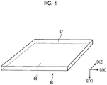
Fig. 4 is a schematic diagram showing the shape of a thermally conductive part. - Hereinafter, a preferred embodiment of the present invention will be described in detail with reference to the accompanying drawings. The present invention is not limited by this embodiment, and in a case where there are a plurality of embodiments, configurations made by combining the respective embodiments are also included in the present invention.
-
Fig. 1 is a schematic diagram showing the configuration of a solid laser device in this embodiment. Asolid laser device 1 according to this embodiment is a device for performing irradiation of a solid laser using a solid for a medium and is a slab type solid laser irradiation device. As shown inFig. 1 , thesolid laser device 1 has a solidlaser amplification device 10, anaccommodation chamber 12, alight emitting part 100, and anirradiation part 102. Thelight emitting part 100 is an excitation light source of a laser light L and is, for example, a laser diode. Theirradiation part 102 is, for example, a laser irradiation head. Thesolid laser device 1 makes the laser light L excited in thelight emitting part 100 pass through the solidlaser amplification device 10 provided in theaccommodation chamber 12, thereby amplifying the laser light L, and irradiates the amplified laser light L from theirradiation part 102. Thesolid laser device 1 performs machining or the like with the irradiation of the laser light L from theirradiation part 102. The laser light L which is irradiated by thesolid laser device 1 is a laser light having high output of 100 W/cm2 or more, for example. - As shown in
Fig. 1 , theaccommodation chamber 12 is a chamber for accommodating the solidlaser amplification device 10 therein. Theaccommodation chamber 12 is a chamber hermetically sealed from the outside, and in use, gas in the interior thereof is discharged by a pump or the like, so that theaccommodation chamber 12 is in a vacuum state. Anentrance window 12a and anexit window 12b are provided in theaccommodation chamber 12, and thus the laser light L from thelight emitting part 100 is transmitted to the interior through theentrance window 12a and the laser light L in the interior is emitted from theexit window 12b to theirradiation part 102. - The solid
laser amplification device 10 is an amplifying device of a so-called slab type solid laser. The solidlaser amplification device 10 has a laser medium part 20,cooling parts conductive parts - The laser medium part 20 is a slab type laser medium for amplifying the laser light L. In this embodiment, the laser medium part 20 is Nd:YAG ceramics. The Nd:YAG ceramics is obtained by partially doping yttrium with neodymium in a process of producing a crystal of YAG (Yttrium Aluminum Garnet). The laser medium part 20 has a medium 22 and
amplification layers medium 22 is a light-transmitting crystal (solid) such as YAG, for example. Theamplification layers medium 22 and are produced by doping ions of yttrium or the like on a plate made of the same material as themedium 22. Theamplification layers - The
medium 22 is a hexahedron (in this embodiment, a frustum). In themedium 22, the length thereof along a direction X is longer than the length along a direction Y. The direction Y is a direction crossing the direction X, and in this embodiment, it is a direction orthogonal to the direction X. Further, a direction Z (described later) is a direction crossing the direction X and the direction Y, and in this embodiment, it is a direction orthogonal to the direction X and the direction Y. In the medium 22, a surface on one side along the direction Y is anupper bottom surface 22a on the smaller area side, and a surface on the other side is alower bottom surface 22b on the larger area side. However, the shape of the medium 22 is not limited thereto. - The amplification layers 24A and 24C are mounted on the
lower bottom surface 22b with a predetermined interval therebetween along the direction X. Theamplification layer 24B is mounted on theupper bottom surface 22a. Theamplification layer 24B is located between theamplification layer 24A and theamplification layer 24C along the direction X. Only one amplification layer 22B is mounted on theupper bottom surface 22a. However, similar to thelower bottom surface 22b, a plurality of amplification layers may be mounted on theupper bottom surface 22a with predetermined intervals. - Hereinafter, the amplification layers 24A, 24B, and 24C will be referred to as an
amplification layer 24 in a case where they are not distinguished from each other. It can be said that theamplification layer 24 is provided on each of the opposite surfaces (theupper bottom surface 22a and the lower bottom surface 24b) of the medium 22 along the direction Y. Further, it can be said that a plurality of amplification layers 24 are provided on the surface of the medium 22 at predetermined intervals along the direction X. However, the amplification layers 24 may not be provided at predetermined intervals along the direction X and may be provided over the entirety of theupper bottom surface 22a and the lower bottom surface 24b. - The laser light L enters the medium 22 from an
entrance part 26 on the side surface of the medium 22. The laser light L entering the medium 22 enters theamplification layer 24. The laser light L entering theamplification layer 24 is amplified and is reflected by asurface 25 that is the surface of theamplification layer 24 on the side opposite to the medium 22. The laser light L reflected by thesurface 25 enters the medium 22 again from theamplification layer 24 and is emitted from anexit part 27 on the side surface on the side opposite to theentrance part 26 along the direction X. A reflective layer which totally reflects the laser light L may be provided on thesurface 25. - In the example of this embodiment, the laser light L entering the
accommodation chamber 12 enters theamplification layer 24A from theentrance part 26 through the medium 22. The laser light L entering theamplification layer 24A is amplified and reflected and enters theamplification layer 24B through the medium 22. The laser light L entering theamplification layer 24B is amplified and reflected and enters theamplification layer 24C through the medium 22. The laser light L entering theamplification layer 24C is amplified and reflected, enters the medium 22, and is emitted from theexit part 27 toward the outside (the accommodation chamber 12). In this manner, the laser light L in this embodiment advances in a zigzag manner in the direction X in the laser medium part 20. Therefore, the direction X can also be referred to as a traveling direction of the laser light L. - Next, the
cooling parts cooling parts part 30 in a case where they are not distinguished from each other.Fig. 2 is a schematic diagram of the cooling part in this embodiment. The coolingpart 30 is a microchannel type heat exchanger. As shown inFig. 2 , the coolingpart 30 has amicrochannel part 31, aninlet header part 32, and anoutlet header part 34. - The
microchannel part 31 is a plate-shaped member having a plurality offlow paths 36 opened therein. Theflow paths 36 extend along a direction A parallel to asurface 31a of themicrochannel part 31. Theflow paths 36 are open on aside surface 31b on one side and aside surface 31c on the other side of themicrochannel part 31 along the direction A and pass through from theside surface 31b on one side to theside surface 31c on the other side. A plurality of (in this embodiment, five)flow paths 36 are arranged along a direction B which is a direction parallel to thesurface 31a of themicrochannel part 31 and crosses the direction A. In this embodiment, themicrochannel part 31 is a metal member having a relatively high thermal conductivity, such as aluminum or SUS (stainless steel). However, the material is not limited thereto. - The
inlet header part 32 is a tubular member having a hollow inside. Theinlet header part 32 is mounted on theside surface 31b on one side of themicrochannel part 31. Theinlet header part 32 has an opening portion (not shown) for making the internal space thereof communicate with each of the plurality offlow paths 36, and anintroduction opening portion 32a for introducing a cooling solvent W into the internal space. - The
outlet header part 34 is a tubular member having a hollow inside. Theoutlet header part 34 is mounted on theside surface 31b on the other side of themicrochannel part 31. Theoutlet header part 34 has an opening portion (not shown) for making the internal space thereof communicate with each of the plurality offlow paths 36, and a lead-outopening portion 34a for introducing the cooling solvent W from the internal space to the outside. - In the cooling
part 30, the cooling solvent W is introduced from theintroduction opening portion 32a into theinlet header part 32, is distributed to therespective flow paths 36, and flows through therespective flow paths 36. Themicrochannel part 31 is in contact with an object to be cooled and cools the object to be cooled by the cooling solvent W flowing through therespective flow paths 36. The cooling solvent W flowing through therespective flow paths 36 flows toward theoutlet header part 34. The cooling solvent W flowing into theoutlet header part 34 is led out from the lead-outopening portion 34a to the outside, cooled on the outside, and introduced into theinlet header part 32 again. The cooling solvent W in this embodiment is a liquid in a state of being introduced into theinlet header part 32 and is, for example, liquid nitrogen, water, or the like. -
Fig. 3 is a schematic diagram of the solid laser amplification device in this embodiment, as viewed from above. As shown inFigs. 1 and3 , thesurface 31a of each of thecooling parts 30 is mounted on asurface 42 of theamplification layer 24 with each of the thermallyconductive parts part 30 cools theamplification layer 24. The coolingpart 30A is mounted on theamplification layer 24A. The coolingpart 30B is mounted on theamplification layer 24B. The coolingpart 30C is mounted on theamplification layer 24C. Therefore, it can be said that the coolingpart 30 is provided on each of the opposite surfaces (the surface on theupper bottom surface 22a side, and the surface on the lower bottom surface 24b side) of the laser medium part 20 along the direction Y. Further, it can be said that a plurality ofcooling parts 30 are provided on the surface of the laser medium part 20 at predetermined intervals along the direction X. That is, the coolingpart 30 is provided at only theamplification layer 24 which reaches a high temperature by receiving (amplifying and reflecting) the laser light L, in the laser medium part 20. The coolingpart 30 is mounted on eachamplification layer 24 such that the direction A in which theflow path 36 extends is along the direction Z and the direction B in which the plurality offlow paths 36 are arranged is along the direction X. However, the mounting direction of the coolingpart 30 is not limited thereto as long as thesurface 31a is mounted on thesurface 42 of theamplification layer 24, and for example, the direction A in which theflow path 36 extends may be along the direction X. - Further, as shown in
Fig. 1 , the coolingpart 30 is connected to a coolingsolvent cooling part 50. Specifically, the coolingsolvent cooling part 50 is provided outside theaccommodation chamber 12, and the cooling solvent W is introduced into theintroduction opening portion 32a of theinlet header part 32 through anintroduction pipe 52. Further, in the coolingsolvent cooling part 50, the cooling solvent W is led out from the lead-outopening portion 34a of theoutlet header part 34 through a lead-outpipe 54. The coolingsolvent cooling part 50 cools the cooling solvent W from theoutlet header part 34 and supplies it to theinlet header part 32 again. The coolingsolvent cooling part 50 may have any configuration as long as it cools the cooling solvent W, and for example, the coolingsolvent cooling part 50 may has a configuration in which natural cooling is performed by providing fins between a plurality of tubes through which the cooling solvent W passes, or a configuration in which forced cooling is performed. - Next, the thermally
conductive parts conductive parts conductive part 40 in a case where they are not distinguished from each other.Fig. 4 is a schematic diagram showing the shape of the thermally conductive part. As shown inFigs. 1 and4 , the thermallyconductive part 40 is a plate-shaped member having high thermal conductivity, is provided in contact with theamplification layer 24 and the coolingpart 30 between theamplification layer 24 and the coolingpart 30, and transfers the heat of theamplification layer 24 to the coolingpart 30. It is preferable that the thermallyconductive part 40 is fixedly provided in close contact with theamplification layer 24 and the coolingpart 30 between theamplification layer 24 and the coolingpart 30. Specifically, in the thermallyconductive part 40A, thesurface 42 on one side is in contact with thesurface 25 of theamplification layer 24A and asurface 44 on the other side is in contact with thesurface 31a of thecooling part 30A. Similarly, in the thermallyconductive part 40B, thesurface 42 on one side is in contact with thesurface 25 of theamplification layer 24B and thesurface 44 on the other side is in contact with thesurface 31a of thecooling part 30B. Similarly, in the thermallyconductive part 40C, thesurface 42 on one side is in contact with thesurface 25 of theamplification layer 24C and thesurface 44 on the other side is in contact with thesurface 31a of thecooling part 30C. Therefore, it can be said that the thermallyconductive part 40 is provided on each of the opposite surfaces (the surface on theupper bottom surface 22a side and the surface on the lower bottom surface 24b side) of the laser medium part 20 along the direction Y. Further, it can be said that a plurality of thermallyconductive parts 40 are provided on the surface of the laser medium part 20 at predetermined intervals along the direction X. In other words, the thermallyconductive part 40 is provided at only theamplification layer 24 which reaches a high temperature by receiving the laser light L, in the laser medium part 20. - The thermally
conductive part 40 is made of a material having thermal conductivity higher than those of the laser medium part 20 and the coolingpart 30, and in this embodiment, it is a graphite sheet. The graphite sheet is a sheet which includes graphite, and is formed by extending, for example, a mixture of graphite powder and binder resin, or expanded graphite, in a sheet form. In the thermallyconductive part 40 in this embodiment, graphite layers extending along directions C and D which are directions parallel to the surfaces (thesurface 42 on one side and thesurface 44 on the other side) are laminated along a direction E which is a direction perpendicular to the surfaces. The graphite layer is oriented along directions (for example, the directions C and D) parallel to the surface and has an anisotropy in thermal conductivity. Specifically, in the thermallyconductive part 40, the thermal conductivity thereof along the direction C and the direction D is higher than the thermal conductivity along the direction E. That is, in the thermallyconductive part 40, heat is transmitted more easily along the direction C and the direction D than the direction E. The thickness of the thermallyconductive part 40 in this embodiment is greater than or equal to 0.1 mm and less than or equal to 1 mm. However, there is no limitation thereto. - The thermally
conductive part 40 is mounted such that thesurface 42 on one side is in contact with thesurface 25 of theamplification layer 24 and thesurface 44 on the other side is in contact with thesurface 31a of the coolingpart 30. Further, the thermallyconductive part 40 is mounted such that the direction C is a direction parallel to the direction X, the direction D is a direction parallel to the direction Z, and the direction E is a direction parallel to the direction Y. However, the mounting direction of the thermallyconductive part 40 is not limited thereto as long as the direction E is a direction parallel to the direction Y. - The solid
laser amplification device 10 described above has the laser medium part 20 having the medium 22 and theamplification layer 24, the coolingpart 30, and the thermallyconductive part 40. The medium 22 is a solid laser medium into which the laser light L enters from theentrance part 26 and from which the laser light L is emitted from theexit part 27 to the outside. Further, theamplification layer 24 is provided on the surface of the medium 22, receives the laser light L in the medium 22, and amplifies and reflects the laser light L toward theexit part 27. Further, the coolingpart 30 is a microchannel type heat exchanger which cools theamplification layer 24. Further, the thermallyconductive part 40 is provided in contact with theamplification layer 24 and the coolingpart 30 between theamplification layer 24 and the coolingpart 30 and transfers the heat of theamplification layer 24 to the coolingpart 30. - In the solid
laser amplification device 10, the laser light L enters theamplification layer 24, and therefore, theamplification layer 24 is heated by the laser light L. The microchanneltype cooling part 30 is mounted on theamplification layer 24 with the thermallyconductive part 40 interposed therebetween. Therefore, the heat of theamplification layer 24 is transferred to the coolingpart 30 through the thermallyconductive part 40 and indirectly cooled by the cooling solvent W flowing in the coolingpart 30. The solidlaser amplification device 10 performs indirect cooling, and therefore, unlike direct cooling in which liquid nitrogen is injected to, for example, the laser medium part 20 (the amplification layer 24), it is not necessary to perform sealing in order to cool the laser medium part 20. Therefore, according to the solidlaser amplification device 10, it is possible to properly cool the laser medium part 20. Further, in the solidlaser amplification device 10, heat is transferred to the coolingpart 30 through the thermallyconductive part 40. Therefore, in the solidlaser amplification device 10, it is possible to efficiently transfer the heat of theamplification layer 24 to the coolingpart 30, and thus it is possible to more properly cool theamplification layer 24. - Further, in the solid
laser amplification device 10, theamplification layer 24, the coolingpart 30, and the thermallyconductive part 40 are provided on each of the opposite surfaces of the medium 22 along the direction Y. Therefore, in the solidlaser amplification device 10, it is possible to reliably provide the coolingpart 30 and the thermallyconductive part 40 at a place (in this embodiment, theamplification layer 24 provided on a bottom surface 23 of the medium 22) which easily reaches a high temperature by receiving the laser light L, in the slab-type solid laser in which the laser light L advances in a zigzag manner. Therefore, in the solidlaser amplification device 10, it is possible to more efficiently remove the heat of theamplification layer 24 and more properly cool theamplification layer 24. - Further, in the solid
laser amplification device 10, a plurality ofcooling parts 30 and a plurality of thermallyconductive parts 40 are provided at predetermined intervals along a traveling direction of the laser light L (the direction X). According to the solidlaser amplification device 10, the coolingpart 30 and the thermallyconductive part 40 can be provided at only a place (in this embodiment, theamplification layer 24 provided on the bottom surface 23 of the medium 22) which easily reaches a high temperature by receiving the laser light L. For this reason, in the solidlaser amplification device 10, it is possible to further cool a high temperature part than a low temperature part and it is possible to suppress the bias of a temperature distribution in the laser medium part 20. In this way, in the solidlaser amplification device 10, it is possible to suppress a decrease in the performance of the laser light L. - Further, in the solid
laser amplification device 10, the thermallyconductive part 40 is a graphite sheet, thesurface 42 on one side thereof is in contact with theamplification layer 24, and thesurface 44 on the other side is in contact with the coolingpart 30. The thermallyconductive part 40 is a graphite sheet having high thermal conductivity, and therefore, it is possible to more efficiently transfer the heat of theamplification layer 24 to the coolingpart 30 and it is possible to more properly cool theamplification layer 24. However, the thermallyconductive part 40 is not limited to being a graphite sheet, and any material can be used as long as it can efficiently transfer the heat of theamplification layer 24 to the coolingpart 30. - Further, in the thermally
conductive part 40, the thermal conductivity thereof along the directions (the directions C and D) parallel to thesurface 42 on one side is higher than the thermal conductivity along the direction (the direction E) crossing thesurface 42 on one side. Therefore, in the solidlaser amplification device 10, it is possible to diffuse the heat of theamplification layer 24 in a surface direction of the thermallyconductive part 40 and cool the heat on theentire surface 31a of the coolingpart 30. Therefore, the thermallyconductive part 40 can more properly cool theamplification layer 24. Further, in the solidlaser amplification device 10, the heat of theamplification layer 24 is diffused in the surface direction of the thermallyconductive part 40, and therefore, the heat of theamplification layer 24 is made uniform along the surface, so that it is also possible to suppress the bias of a temperature distribution in the laser medium part 20. - However, in the thermally
conductive part 40, the thermal conductivity thereof along the directions (the directions C and D) parallel to thesurface 42 on one side may be lower than the thermal conductivity along the direction (the direction E) crossing thesurface 42 on one side. In this case, the graphite layers extending along the direction E are laminated along the direction C or the direction D. In this case, heat can be rapidly transferred in the direction E, that is, in the direction toward the coolingpart 30 from theamplification layer 24, and therefore, it becomes possible to more rapidly cool theamplification layer 24. - In this embodiment, the
microchannel part 31 is a metal member. However, at least thesurface 31a that is a surface which is in contact with the thermallyconductive part 40 may be configured of a graphite sheet, similar to the thermallyconductive part 40. In this case, the thermal conductivity of themicrochannel part 31 itself becomes higher, and therefore, it is possible to more properly cool theamplification layer 24. In this case, it is preferable that a place between thesurface 31a and the plurality offlow paths 36 is configured by laminating graphite sheets. In the graphite sheet, similar to the thermallyconductive part 40, the graphite layers extending in the directions A and B parallel to thesurface 31a may be laminated along the direction crossing the directions A and B, or the graphite layers extending along the direction crossing the directions A and B may be laminated along the direction A or the direction B. - The present embodiment of the present invention has been described above. However, an embodiment is not limited by the content of this embodiment. Further, in the constituent elements described above, constituent elements which can be easily anticipated by those skilled in the art, constituent elements which are substantially equal to the constituent elements described above, and so-called equivalents are included. Further, it is possible to appropriately combine the constituent elements described above. Further, various omissions, substitutions, or changes of constituent elements can be made within a scope which does not depart from the gist of the present embodiment described above.
-
- 1: solid laser device
- 10: solid laser amplification device
- 12: accommodation chamber
- 12a: entrance window
- 12b: exit window
- 20: laser medium part
- 22: medium
- 24, 24A, 24B, 24C: amplification layer
- 25: surface
- 26: entrance part
- 27: exit part
- 30, 30A, 30B, 30C: cooling part
- 31: microchannel part
- 31a: surface
- 31b, 31c: side surface
- 32: inlet header part
- 32a: introduction opening portion
- 34: outlet header part
- 34a: lead-out opening portion
- 36: flow path
- 40, 40A, 40B, 40C: thermally conductive part
- 42, 44: surface
- 50: cooling solvent cooling part
- 52: introduction pipe
- 54: lead-out pipe
- 100: light emitting part
- 102: irradiation part
- A, B, C, D, E, X, Y, Z: direction
- L: laser light
- W: cooling solvent
Claims (7)
- A solid laser amplification device comprising:a laser medium part which has a solid medium, into which a laser light enters from an entrance part and from which the laser light is emitted from an exit part to the outside, and an amplification layer which is provided on a surface of the medium, receives the laser light in the medium, and amplifies and reflects the laser light toward the exit part;a microchannel type cooling part which cools the amplification layer; anda thermally conductive part which is provided in contact with the amplification layer and the cooling part between the amplification layer and the cooling part and transfers heat of the amplification layer to the cooling part.
- The solid laser amplification device according to claim 1, wherein the amplification layer, the thermally conductive part, and the cooling part are provided on each of the opposite surfaces of the medium.
- The solid laser amplification device according to claim 2, wherein a plurality of the cooling parts and a plurality of the thermally conductive parts are provided at predetermined intervals along a traveling direction of the laser light.
- The solid laser amplification device according to any one of claims 1 to 3, wherein the thermally conductive part is a graphite sheet, a surface on one side of the thermally conductive part is in contact with the amplification layer, and a surface on the other side is in contact with the cooling part.
- The solid laser amplification device according to claim 4, wherein in the thermally conductive part, thermal conductivity thereof along a direction parallel to the surface on one side is higher than thermal conductivity thereof along a direction crossing the surface on one side.
- The solid laser amplification device according to claim 4, wherein in the thermally conductive part, thermal conductivity thereof along a direction parallel to the surface on one side is lower than thermal conductivity thereof along a direction crossing the surface on one side.
- The solid laser amplification device according to any one of claims 1 to 6, wherein a surface of the cooling part, with which the thermally conductive part is in contact, is a graphite sheet.
Applications Claiming Priority (2)
| Application Number | Priority Date | Filing Date | Title |
|---|---|---|---|
| JP2015204802A JP6632315B2 (en) | 2015-10-16 | 2015-10-16 | Solid-state laser amplifier |
| PCT/JP2016/067060 WO2017064881A1 (en) | 2015-10-16 | 2016-06-08 | Solid laser amplification device |
Publications (3)
| Publication Number | Publication Date |
|---|---|
| EP3288127A1 true EP3288127A1 (en) | 2018-02-28 |
| EP3288127A4 EP3288127A4 (en) | 2018-09-26 |
| EP3288127B1 EP3288127B1 (en) | 2021-03-10 |
Family
ID=58518114
Family Applications (1)
| Application Number | Title | Priority Date | Filing Date |
|---|---|---|---|
| EP16855135.6A Active EP3288127B1 (en) | 2015-10-16 | 2016-06-08 | Solid laser amplification device |
Country Status (4)
| Country | Link |
|---|---|
| US (1) | US10290991B2 (en) |
| EP (1) | EP3288127B1 (en) |
| JP (1) | JP6632315B2 (en) |
| WO (1) | WO2017064881A1 (en) |
Families Citing this family (1)
| Publication number | Priority date | Publication date | Assignee | Title |
|---|---|---|---|---|
| JP7086720B2 (en) | 2018-05-30 | 2022-06-20 | 浜松ホトニクス株式会社 | Laser device |
Family Cites Families (14)
| Publication number | Priority date | Publication date | Assignee | Title |
|---|---|---|---|---|
| US3633126A (en) | 1969-04-17 | 1972-01-04 | Gen Electric | Multiple internal reflection face-pumped laser |
| JPS5135207B2 (en) | 1972-10-28 | 1976-10-01 | ||
| JP3338974B2 (en) * | 1995-01-11 | 2002-10-28 | ミヤチテクノス株式会社 | Laser device |
| JPH09181376A (en) | 1995-12-26 | 1997-07-11 | Mitsubishi Heavy Ind Ltd | Semiconductor laser for pumping solid state laser and fabrication thereof |
| US6002695A (en) * | 1996-05-31 | 1999-12-14 | Dpss Lasers, Inc. | High efficiency high repetition rate, intra-cavity tripled diode pumped solid state laser |
| JP2001015844A (en) * | 1999-06-30 | 2001-01-19 | Saifasha:Yugen | Solid laser |
| US6339605B1 (en) * | 2000-02-16 | 2002-01-15 | The Boeing Company | Active mirror amplifier system and method for a high-average power laser system |
| US6625193B2 (en) * | 2001-01-22 | 2003-09-23 | The Boeing Company | Side-pumped active mirror solid-state laser for high-average power |
| US20050189647A1 (en) * | 2002-10-11 | 2005-09-01 | Chien-Min Sung | Carbonaceous composite heat spreader and associated methods |
| US20060083276A1 (en) * | 2004-09-28 | 2006-04-20 | Snake Creek Lasers, Llc. | Cryogenically cooled solid state lasers |
| US7430230B2 (en) | 2005-04-07 | 2008-09-30 | The Boeing Company | Tube solid-state laser |
| JP2010034413A (en) * | 2008-07-30 | 2010-02-12 | Hamamatsu Photonics Kk | Solid-state laser apparatus |
| FR2969402B1 (en) * | 2010-12-17 | 2013-02-15 | Fibercryst | LASER GAIN MODULE AND METHOD FOR MANUFACTURING SUCH A MODULE |
| JP6003323B2 (en) * | 2012-07-18 | 2016-10-05 | 国立大学法人大阪大学 | LASER MEDIUM UNIT, LASER AMPLIFIER, LASER OSCILLATOR, AND COOLING METHOD |
-
2015
- 2015-10-16 JP JP2015204802A patent/JP6632315B2/en active Active
-
2016
- 2016-06-08 US US15/574,190 patent/US10290991B2/en active Active
- 2016-06-08 EP EP16855135.6A patent/EP3288127B1/en active Active
- 2016-06-08 WO PCT/JP2016/067060 patent/WO2017064881A1/en not_active Ceased
Also Published As
| Publication number | Publication date |
|---|---|
| EP3288127B1 (en) | 2021-03-10 |
| US20180145473A1 (en) | 2018-05-24 |
| US10290991B2 (en) | 2019-05-14 |
| EP3288127A4 (en) | 2018-09-26 |
| JP6632315B2 (en) | 2020-01-22 |
| JP2017076750A (en) | 2017-04-20 |
| WO2017064881A1 (en) | 2017-04-20 |
Similar Documents
| Publication | Publication Date | Title |
|---|---|---|
| US6859472B2 (en) | Multi-jet impingement cooled slab laser pumphead and method | |
| US20040114657A1 (en) | Side-pumped solid-state disk for high-average power | |
| DE602006006816D1 (en) | SIDE PUMPED TUBE SOLID BODY LASER | |
| CN113937615A (en) | Cooling assembly and cooling method for laser | |
| US20160315445A1 (en) | High flux diode packaging using passive microscale liquid-vapor phase change | |
| US9762018B2 (en) | System and method for cooling a laser gain medium using an ultra-thin liquid thermal optical interface | |
| US10290991B2 (en) | Solid laser amplification device | |
| CN104953446A (en) | Novel diode-pumping immersion-type liquid-cooling solid laser gain pool | |
| US10236655B2 (en) | Solid laser amplification device | |
| FI4085225T3 (en) | Heat exchanger for cryogenic cooling apparatus | |
| US10203461B2 (en) | Techniques for forming waveguides for use in laser systems or other systems and associated devices | |
| Nikolaenko et al. | Using laser radiation for the formation of capillary structure in flat ceramic heat pipes | |
| US20170373457A1 (en) | Waveguide for diode-pumped alkali lasers | |
| US20070189346A1 (en) | Solid-state laser apparatus | |
| CN100379099C (en) | laser oscillator | |
| US10777966B1 (en) | Mixed-flow cooling to maintain cooling requirements | |
| Tsunekane et al. | Design and performance of compact heatsink for high-power diode edge-pumped, microchip lasers | |
| JP4925059B2 (en) | Solid state laser module | |
| KR102332955B1 (en) | laser pump chamber device | |
| US12630423B2 (en) | Ozoniser and method for producing ozone from oxygen | |
| KR100733200B1 (en) | Laser oscillator | |
| EP4415189A1 (en) | Laser medium unit, laser amplification device, and laser oscillation device | |
| KR101034658B1 (en) | Optical amplifiers in the form of distributed disks | |
| CN204179474U (en) | A kind of slab laser amplifier | |
| JP3951782B2 (en) | Semiconductor laser pumped solid state laser amplifier, semiconductor laser pumped solid state laser apparatus, and semiconductor laser cooling method in semiconductor laser pumped solid state laser amplifier |
Legal Events
| Date | Code | Title | Description |
|---|---|---|---|
| STAA | Information on the status of an ep patent application or granted ep patent |
Free format text: STATUS: THE INTERNATIONAL PUBLICATION HAS BEEN MADE |
|
| PUAI | Public reference made under article 153(3) epc to a published international application that has entered the european phase |
Free format text: ORIGINAL CODE: 0009012 |
|
| STAA | Information on the status of an ep patent application or granted ep patent |
Free format text: STATUS: REQUEST FOR EXAMINATION WAS MADE |
|
| 17P | Request for examination filed |
Effective date: 20171120 |
|
| AK | Designated contracting states |
Kind code of ref document: A1 Designated state(s): AL AT BE BG CH CY CZ DE DK EE ES FI FR GB GR HR HU IE IS IT LI LT LU LV MC MK MT NL NO PL PT RO RS SE SI SK SM TR |
|
| AX | Request for extension of the european patent |
Extension state: BA ME |
|
| A4 | Supplementary search report drawn up and despatched |
Effective date: 20180827 |
|
| RIC1 | Information provided on ipc code assigned before grant |
Ipc: H01S 3/10 20060101ALI20180817BHEP Ipc: H01S 3/063 20060101ALI20180817BHEP Ipc: H01S 3/02 20060101ALN20180817BHEP Ipc: H01S 3/042 20060101AFI20180817BHEP Ipc: H01S 3/04 20060101ALI20180817BHEP Ipc: H01S 3/06 20060101ALI20180817BHEP Ipc: H01S 3/23 20060101ALN20180817BHEP |
|
| DAV | Request for validation of the european patent (deleted) | ||
| DAX | Request for extension of the european patent (deleted) | ||
| REG | Reference to a national code |
Ref country code: DE Ref legal event code: R079 Ref document number: 602016054200 Country of ref document: DE Free format text: PREVIOUS MAIN CLASS: H01S0003042000 Ipc: H01S0003040000 |
|
| GRAP | Despatch of communication of intention to grant a patent |
Free format text: ORIGINAL CODE: EPIDOSNIGR1 |
|
| STAA | Information on the status of an ep patent application or granted ep patent |
Free format text: STATUS: GRANT OF PATENT IS INTENDED |
|
| RIC1 | Information provided on ipc code assigned before grant |
Ipc: H01S 3/16 20060101ALI20201110BHEP Ipc: H01S 3/00 20060101ALI20201110BHEP Ipc: H01S 3/23 20060101ALI20201110BHEP Ipc: H01S 3/042 20060101ALI20201110BHEP Ipc: H01S 3/04 20060101AFI20201110BHEP Ipc: H01S 3/02 20060101ALI20201110BHEP Ipc: H01S 3/06 20060101ALI20201110BHEP |
|
| INTG | Intention to grant announced |
Effective date: 20201209 |
|
| GRAS | Grant fee paid |
Free format text: ORIGINAL CODE: EPIDOSNIGR3 |
|
| GRAA | (expected) grant |
Free format text: ORIGINAL CODE: 0009210 |
|
| STAA | Information on the status of an ep patent application or granted ep patent |
Free format text: STATUS: THE PATENT HAS BEEN GRANTED |
|
| AK | Designated contracting states |
Kind code of ref document: B1 Designated state(s): AL AT BE BG CH CY CZ DE DK EE ES FI FR GB GR HR HU IE IS IT LI LT LU LV MC MK MT NL NO PL PT RO RS SE SI SK SM TR |
|
| REG | Reference to a national code |
Ref country code: GB Ref legal event code: FG4D |
|
| REG | Reference to a national code |
Ref country code: AT Ref legal event code: REF Ref document number: 1370858 Country of ref document: AT Kind code of ref document: T Effective date: 20210315 Ref country code: CH Ref legal event code: EP |
|
| REG | Reference to a national code |
Ref country code: IE Ref legal event code: FG4D |
|
| REG | Reference to a national code |
Ref country code: DE Ref legal event code: R096 Ref document number: 602016054200 Country of ref document: DE |
|
| REG | Reference to a national code |
Ref country code: LT Ref legal event code: MG9D |
|
| PG25 | Lapsed in a contracting state [announced via postgrant information from national office to epo] |
Ref country code: HR Free format text: LAPSE BECAUSE OF FAILURE TO SUBMIT A TRANSLATION OF THE DESCRIPTION OR TO PAY THE FEE WITHIN THE PRESCRIBED TIME-LIMIT Effective date: 20210310 Ref country code: FI Free format text: LAPSE BECAUSE OF FAILURE TO SUBMIT A TRANSLATION OF THE DESCRIPTION OR TO PAY THE FEE WITHIN THE PRESCRIBED TIME-LIMIT Effective date: 20210310 Ref country code: GR Free format text: LAPSE BECAUSE OF FAILURE TO SUBMIT A TRANSLATION OF THE DESCRIPTION OR TO PAY THE FEE WITHIN THE PRESCRIBED TIME-LIMIT Effective date: 20210611 Ref country code: NO Free format text: LAPSE BECAUSE OF FAILURE TO SUBMIT A TRANSLATION OF THE DESCRIPTION OR TO PAY THE FEE WITHIN THE PRESCRIBED TIME-LIMIT Effective date: 20210610 Ref country code: BG Free format text: LAPSE BECAUSE OF FAILURE TO SUBMIT A TRANSLATION OF THE DESCRIPTION OR TO PAY THE FEE WITHIN THE PRESCRIBED TIME-LIMIT Effective date: 20210610 Ref country code: LT Free format text: LAPSE BECAUSE OF FAILURE TO SUBMIT A TRANSLATION OF THE DESCRIPTION OR TO PAY THE FEE WITHIN THE PRESCRIBED TIME-LIMIT Effective date: 20210310 |
|
| REG | Reference to a national code |
Ref country code: AT Ref legal event code: MK05 Ref document number: 1370858 Country of ref document: AT Kind code of ref document: T Effective date: 20210310 |
|
| REG | Reference to a national code |
Ref country code: NL Ref legal event code: MP Effective date: 20210310 |
|
| PG25 | Lapsed in a contracting state [announced via postgrant information from national office to epo] |
Ref country code: RS Free format text: LAPSE BECAUSE OF FAILURE TO SUBMIT A TRANSLATION OF THE DESCRIPTION OR TO PAY THE FEE WITHIN THE PRESCRIBED TIME-LIMIT Effective date: 20210310 Ref country code: LV Free format text: LAPSE BECAUSE OF FAILURE TO SUBMIT A TRANSLATION OF THE DESCRIPTION OR TO PAY THE FEE WITHIN THE PRESCRIBED TIME-LIMIT Effective date: 20210310 Ref country code: SE Free format text: LAPSE BECAUSE OF FAILURE TO SUBMIT A TRANSLATION OF THE DESCRIPTION OR TO PAY THE FEE WITHIN THE PRESCRIBED TIME-LIMIT Effective date: 20210310 |
|
| PG25 | Lapsed in a contracting state [announced via postgrant information from national office to epo] |
Ref country code: NL Free format text: LAPSE BECAUSE OF FAILURE TO SUBMIT A TRANSLATION OF THE DESCRIPTION OR TO PAY THE FEE WITHIN THE PRESCRIBED TIME-LIMIT Effective date: 20210310 |
|
| PG25 | Lapsed in a contracting state [announced via postgrant information from national office to epo] |
Ref country code: AT Free format text: LAPSE BECAUSE OF FAILURE TO SUBMIT A TRANSLATION OF THE DESCRIPTION OR TO PAY THE FEE WITHIN THE PRESCRIBED TIME-LIMIT Effective date: 20210310 Ref country code: SM Free format text: LAPSE BECAUSE OF FAILURE TO SUBMIT A TRANSLATION OF THE DESCRIPTION OR TO PAY THE FEE WITHIN THE PRESCRIBED TIME-LIMIT Effective date: 20210310 Ref country code: EE Free format text: LAPSE BECAUSE OF FAILURE TO SUBMIT A TRANSLATION OF THE DESCRIPTION OR TO PAY THE FEE WITHIN THE PRESCRIBED TIME-LIMIT Effective date: 20210310 Ref country code: CZ Free format text: LAPSE BECAUSE OF FAILURE TO SUBMIT A TRANSLATION OF THE DESCRIPTION OR TO PAY THE FEE WITHIN THE PRESCRIBED TIME-LIMIT Effective date: 20210310 |
|
| PG25 | Lapsed in a contracting state [announced via postgrant information from national office to epo] |
Ref country code: IS Free format text: LAPSE BECAUSE OF FAILURE TO SUBMIT A TRANSLATION OF THE DESCRIPTION OR TO PAY THE FEE WITHIN THE PRESCRIBED TIME-LIMIT Effective date: 20210710 Ref country code: SK Free format text: LAPSE BECAUSE OF FAILURE TO SUBMIT A TRANSLATION OF THE DESCRIPTION OR TO PAY THE FEE WITHIN THE PRESCRIBED TIME-LIMIT Effective date: 20210310 Ref country code: RO Free format text: LAPSE BECAUSE OF FAILURE TO SUBMIT A TRANSLATION OF THE DESCRIPTION OR TO PAY THE FEE WITHIN THE PRESCRIBED TIME-LIMIT Effective date: 20210310 Ref country code: PL Free format text: LAPSE BECAUSE OF FAILURE TO SUBMIT A TRANSLATION OF THE DESCRIPTION OR TO PAY THE FEE WITHIN THE PRESCRIBED TIME-LIMIT Effective date: 20210310 Ref country code: PT Free format text: LAPSE BECAUSE OF FAILURE TO SUBMIT A TRANSLATION OF THE DESCRIPTION OR TO PAY THE FEE WITHIN THE PRESCRIBED TIME-LIMIT Effective date: 20210712 |
|
| REG | Reference to a national code |
Ref country code: DE Ref legal event code: R097 Ref document number: 602016054200 Country of ref document: DE |
|
| PLBE | No opposition filed within time limit |
Free format text: ORIGINAL CODE: 0009261 |
|
| STAA | Information on the status of an ep patent application or granted ep patent |
Free format text: STATUS: NO OPPOSITION FILED WITHIN TIME LIMIT |
|
| PG25 | Lapsed in a contracting state [announced via postgrant information from national office to epo] |
Ref country code: MC Free format text: LAPSE BECAUSE OF FAILURE TO SUBMIT A TRANSLATION OF THE DESCRIPTION OR TO PAY THE FEE WITHIN THE PRESCRIBED TIME-LIMIT Effective date: 20210310 Ref country code: DK Free format text: LAPSE BECAUSE OF FAILURE TO SUBMIT A TRANSLATION OF THE DESCRIPTION OR TO PAY THE FEE WITHIN THE PRESCRIBED TIME-LIMIT Effective date: 20210310 Ref country code: AL Free format text: LAPSE BECAUSE OF FAILURE TO SUBMIT A TRANSLATION OF THE DESCRIPTION OR TO PAY THE FEE WITHIN THE PRESCRIBED TIME-LIMIT Effective date: 20210310 Ref country code: ES Free format text: LAPSE BECAUSE OF FAILURE TO SUBMIT A TRANSLATION OF THE DESCRIPTION OR TO PAY THE FEE WITHIN THE PRESCRIBED TIME-LIMIT Effective date: 20210310 |
|
| REG | Reference to a national code |
Ref country code: CH Ref legal event code: PL |
|
| 26N | No opposition filed |
Effective date: 20211213 |
|
| PG25 | Lapsed in a contracting state [announced via postgrant information from national office to epo] |
Ref country code: SI Free format text: LAPSE BECAUSE OF FAILURE TO SUBMIT A TRANSLATION OF THE DESCRIPTION OR TO PAY THE FEE WITHIN THE PRESCRIBED TIME-LIMIT Effective date: 20210310 |
|
| REG | Reference to a national code |
Ref country code: BE Ref legal event code: MM Effective date: 20210630 |
|
| PG25 | Lapsed in a contracting state [announced via postgrant information from national office to epo] |
Ref country code: LU Free format text: LAPSE BECAUSE OF NON-PAYMENT OF DUE FEES Effective date: 20210608 |
|
| PG25 | Lapsed in a contracting state [announced via postgrant information from national office to epo] |
Ref country code: LI Free format text: LAPSE BECAUSE OF NON-PAYMENT OF DUE FEES Effective date: 20210630 Ref country code: IT Free format text: LAPSE BECAUSE OF FAILURE TO SUBMIT A TRANSLATION OF THE DESCRIPTION OR TO PAY THE FEE WITHIN THE PRESCRIBED TIME-LIMIT Effective date: 20210310 Ref country code: IE Free format text: LAPSE BECAUSE OF NON-PAYMENT OF DUE FEES Effective date: 20210608 Ref country code: CH Free format text: LAPSE BECAUSE OF NON-PAYMENT OF DUE FEES Effective date: 20210630 |
|
| PG25 | Lapsed in a contracting state [announced via postgrant information from national office to epo] |
Ref country code: IS Free format text: LAPSE BECAUSE OF FAILURE TO SUBMIT A TRANSLATION OF THE DESCRIPTION OR TO PAY THE FEE WITHIN THE PRESCRIBED TIME-LIMIT Effective date: 20210710 |
|
| PG25 | Lapsed in a contracting state [announced via postgrant information from national office to epo] |
Ref country code: BE Free format text: LAPSE BECAUSE OF NON-PAYMENT OF DUE FEES Effective date: 20210630 |
|
| PG25 | Lapsed in a contracting state [announced via postgrant information from national office to epo] |
Ref country code: HU Free format text: LAPSE BECAUSE OF FAILURE TO SUBMIT A TRANSLATION OF THE DESCRIPTION OR TO PAY THE FEE WITHIN THE PRESCRIBED TIME-LIMIT; INVALID AB INITIO Effective date: 20160608 |
|
| PG25 | Lapsed in a contracting state [announced via postgrant information from national office to epo] |
Ref country code: CY Free format text: LAPSE BECAUSE OF FAILURE TO SUBMIT A TRANSLATION OF THE DESCRIPTION OR TO PAY THE FEE WITHIN THE PRESCRIBED TIME-LIMIT Effective date: 20210310 |
|
| PG25 | Lapsed in a contracting state [announced via postgrant information from national office to epo] |
Ref country code: MK Free format text: LAPSE BECAUSE OF FAILURE TO SUBMIT A TRANSLATION OF THE DESCRIPTION OR TO PAY THE FEE WITHIN THE PRESCRIBED TIME-LIMIT Effective date: 20210310 |
|
| PG25 | Lapsed in a contracting state [announced via postgrant information from national office to epo] |
Ref country code: MT Free format text: LAPSE BECAUSE OF FAILURE TO SUBMIT A TRANSLATION OF THE DESCRIPTION OR TO PAY THE FEE WITHIN THE PRESCRIBED TIME-LIMIT Effective date: 20210310 |
|
| PGFP | Annual fee paid to national office [announced via postgrant information from national office to epo] |
Ref country code: DE Payment date: 20250429 Year of fee payment: 10 |
|
| PGFP | Annual fee paid to national office [announced via postgrant information from national office to epo] |
Ref country code: GB Payment date: 20250501 Year of fee payment: 10 |
|
| PGFP | Annual fee paid to national office [announced via postgrant information from national office to epo] |
Ref country code: FR Payment date: 20250508 Year of fee payment: 10 |
|
| PG25 | Lapsed in a contracting state [announced via postgrant information from national office to epo] |
Ref country code: TR Free format text: LAPSE BECAUSE OF FAILURE TO SUBMIT A TRANSLATION OF THE DESCRIPTION OR TO PAY THE FEE WITHIN THE PRESCRIBED TIME-LIMIT Effective date: 20210310 |