EP3288039A1 - Bus bar assembly comprising a memory metal composition - Google Patents
Bus bar assembly comprising a memory metal composition Download PDFInfo
- Publication number
- EP3288039A1 EP3288039A1 EP17186503.3A EP17186503A EP3288039A1 EP 3288039 A1 EP3288039 A1 EP 3288039A1 EP 17186503 A EP17186503 A EP 17186503A EP 3288039 A1 EP3288039 A1 EP 3288039A1
- Authority
- EP
- European Patent Office
- Prior art keywords
- bus bar
- memory metal
- distribution system
- additive manufacturing
- manufacturing technique
- Prior art date
- Legal status (The legal status is an assumption and is not a legal conclusion. Google has not performed a legal analysis and makes no representation as to the accuracy of the status listed.)
- Granted
Links
Images


Classifications
-
- H—ELECTRICITY
- H01—ELECTRIC ELEMENTS
- H01B—CABLES; CONDUCTORS; INSULATORS; SELECTION OF MATERIALS FOR THEIR CONDUCTIVE, INSULATING OR DIELECTRIC PROPERTIES
- H01B1/00—Conductors or conductive bodies characterised by the conductive materials; Selection of materials as conductors
- H01B1/02—Conductors or conductive bodies characterised by the conductive materials; Selection of materials as conductors mainly consisting of metals or alloys
- H01B1/026—Alloys based on copper
-
- H—ELECTRICITY
- H01—ELECTRIC ELEMENTS
- H01B—CABLES; CONDUCTORS; INSULATORS; SELECTION OF MATERIALS FOR THEIR CONDUCTIVE, INSULATING OR DIELECTRIC PROPERTIES
- H01B1/00—Conductors or conductive bodies characterised by the conductive materials; Selection of materials as conductors
- H01B1/02—Conductors or conductive bodies characterised by the conductive materials; Selection of materials as conductors mainly consisting of metals or alloys
-
- H—ELECTRICITY
- H01—ELECTRIC ELEMENTS
- H01B—CABLES; CONDUCTORS; INSULATORS; SELECTION OF MATERIALS FOR THEIR CONDUCTIVE, INSULATING OR DIELECTRIC PROPERTIES
- H01B1/00—Conductors or conductive bodies characterised by the conductive materials; Selection of materials as conductors
- H01B1/02—Conductors or conductive bodies characterised by the conductive materials; Selection of materials as conductors mainly consisting of metals or alloys
- H01B1/023—Alloys based on aluminium
-
- H—ELECTRICITY
- H05—ELECTRIC TECHNIQUES NOT OTHERWISE PROVIDED FOR
- H05K—PRINTED CIRCUITS; CASINGS OR CONSTRUCTIONAL DETAILS OF ELECTRIC APPARATUS; MANUFACTURE OF ASSEMBLAGES OF ELECTRICAL COMPONENTS
- H05K7/00—Constructional details common to different types of electric apparatus
- H05K7/14—Mounting supporting structure in casing or on frame or rack
- H05K7/1422—Printed circuit boards receptacles, e.g. stacked structures, electronic circuit modules or box like frames
- H05K7/1427—Housings
- H05K7/1432—Housings specially adapted for power drive units or power converters
- H05K7/14329—Housings specially adapted for power drive units or power converters specially adapted for the configuration of power bus bars
-
- H—ELECTRICITY
- H05—ELECTRIC TECHNIQUES NOT OTHERWISE PROVIDED FOR
- H05K—PRINTED CIRCUITS; CASINGS OR CONSTRUCTIONAL DETAILS OF ELECTRIC APPARATUS; MANUFACTURE OF ASSEMBLAGES OF ELECTRICAL COMPONENTS
- H05K7/00—Constructional details common to different types of electric apparatus
- H05K7/20—Modifications to facilitate cooling, ventilating, or heating
- H05K7/2089—Modifications to facilitate cooling, ventilating, or heating for power electronics, e.g. for inverters for controlling motor
- H05K7/209—Heat transfer by conduction from internal heat source to heat radiating structure
-
- H—ELECTRICITY
- H05—ELECTRIC TECHNIQUES NOT OTHERWISE PROVIDED FOR
- H05K—PRINTED CIRCUITS; CASINGS OR CONSTRUCTIONAL DETAILS OF ELECTRIC APPARATUS; MANUFACTURE OF ASSEMBLAGES OF ELECTRICAL COMPONENTS
- H05K2201/00—Indexing scheme relating to printed circuits covered by H05K1/00
- H05K2201/10—Details of components or other objects attached to or integrated in a printed circuit board
- H05K2201/10227—Other objects, e.g. metallic pieces
- H05K2201/10272—Busbars, i.e. thick metal bars mounted on the printed circuit board [PCB] as high-current conductors
-
- H—ELECTRICITY
- H10—SEMICONDUCTOR DEVICES; ELECTRIC SOLID-STATE DEVICES NOT OTHERWISE PROVIDED FOR
- H10W—GENERIC PACKAGES, INTERCONNECTIONS, CONNECTORS OR OTHER CONSTRUCTIONAL DETAILS OF DEVICES COVERED BY CLASS H10
- H10W72/00—Interconnections or connectors in packages
- H10W72/071—Connecting or disconnecting
- H10W72/073—Connecting or disconnecting of die-attach connectors
Definitions
- the present disclosure relates to bus bars, and more particularly, to systems and methods of utilizing memory metal and/or additive manufacturing in bus bar assemblies.
- a bus bar is a length of material or bar of copper, brass or aluminum that conducts electricity as part of a switchboard or other electrical apparatus.
- a bus bar may be an electrical conductor, configured to maintain a specific voltage and capable of carrying a high current, typically used to make a common connection between several circuits in a system.
- Solid state electronics may generate heat at die interfaces and attachment locations during operation. This heat may result in thermal expansion of components. The heat dissipated by a bus bar and its thermal expansion may be a limiting design factor and/or an important system design consideration.
- the present disclosure relates to a bus bar.
- the bus bar may be formed from a composition of materials.
- the bus bar may be formed by an additive manufacturing technique (e.g. cold spraying of particles of conductive material on a memory metal framework substrate).
- the bus bar, connection points, and various attributes may also be formed by ultrasonic additive manufacturing wherein the memory metal is embedded into a metal matrix created by the successive addition of metal foil.
- the composition of the memory metal and the electrically conductive material may have a substantially net zero coefficient of thermal expansion during operation of the bus bar (e.g., in response to current being delivered through the bus bar at normal operating levels).
- the present disclosure relates to an electrical distribution system.
- the electrical distribution system may include a power source and a common connection between a plurality of components.
- the power source may be electrically coupled to the plurality of components via the common connection.
- the common connection may be formed by additive manufacturing an electrically conductive material onto a memory metal substrate framework.
- the present disclosure also relates to a method of making a bus bar comprising applying an electrically conductive material to a memory metal internal framework through an additive manufacturing technique.
- the composition of the memory metal internal framework and the electrically conductive material may comprise a substantially net zero coefficient of thermal expansion during operation of the bus bar.
- Removing heat from a device in a direct and efficient fashion is desirable.
- multiple layers of material are added to account for the thermal expansion of the electrical components and in particular the thermal expansion of a bus bar.
- thermal interfaces are needed for each layer of a circuit board. Multiple thermal interfaces, such as thermal interfaces between bus work and a circuit board, may result in the part running at an elevated temperature during normal operation. This may result is a shortened lifespan of the circuit board. By removing these additional interfaces, a more efficient throughput of heat delivery to a cooling medium is achieved.
- a bus bar 100 is disclosed. At least a portion of bus bar 100 is formed from a plurality of materials. For instance, a first portion of bus bar 100 may be formed from a traditional bus bar material, such as brass, nickel, silver, gold, zinc, iron, copper or aluminum. A second portion of bus bar 100 may be formed from a memory metal, shape alloy or smart metal.
- the memory metal may be a shape memory alloy, such as nitinol wire (nickel titanium alloy). Nitinol is a nickel-titanium alloy distinguished from other materials by its shape memory and super-elastic characteristics. Shape memory alloys are able to show an elastic deformation behavior.
- a super-elastic characteristic may be referred to as a mechanical shape memory effect or super elasticity.
- Super-elasticity is caused by the stress-induced phase transformation from a high temperature phase into a low temperature phase. The strain related to this phase transformation is fully reversible after removing the stress.
- bus bar 100 may be formed from an aluminum matrix with nitinol wires embedded into this matrix. Bus bar 100 may be designed and/or scaled to carry any desired voltage or power.
- nitinol wire a shape memory alloy
- solder pads such as a copper solder pad and/or conductive traces may also be additively manufactured on a surface, such as a top surface, of the bus bar for die attach points.
- This layout may be configured to provide adequate solderability for a device coupled to a surface of the device.
- Direct write additive manufacturing technologies may be used to form the wire bonds from the silicon/silicon carbide die to the bus bar.
- An exothermic soldering process using an amorphous material (Nanofoil) clad on both sides with solder material may be used to bond a silicon/silicon carbide dies to the bus bar die attach points.
- the additive manufacturing technique 101 may include ultrasonic consolidation (or ultrasonic additive manufacturing), cold spray and/or the like.
- the term "cold spray” as used herein may include a process by which particulates 160 are deposited by means of ballistic impingement upon a suitable substrate 180 at supersonic velocities to form a coating 170 or a free-standing structure.
- the ballistic impingement may be via a supersonic nozzle 150.
- the particles 160 may be fed by feeder system 130 which may toggle between various source material stocks. Also, pressure and heat may be provided by the feeder system 130.
- the melting of particles that occurs during most thermal spray processes can result in oxidation of both the coating and substrate materials.
- the resulting oxides decrease the adhesive and cohesive strengths of the coating.
- the cold spray process may avoid such reactions. Cold spay process may be highly precise if desired allowing for materials to be formed in particular patterns and orientations.
- Nitinol wire 210 elements may be arranged in predetermined orientations, such as arranged along a common plane with spaces between the nitinol wire 210 to form substrate 180.
- Layers of material such as aluminum, may be added, to substrate 180 such as through an additive manufacturing technique 101. Layers adding thickness may be added in any direction of bus bar 100.
- Copper 250, such as a portion or layer of copper 250 may be added to a top surface or bottom surface of bus bar 100. The layer of copper 250 may be formed through an additive manufacturing technique 101.
- Insulation 260 layers may be formed on bus bar 100 where desired. Insulation 260 may be made from any desired material.
- the insulation 260 is configured to electrically shield the interface between two or more components. Insulation 260 layers may be direct write insulation layers formed through the additive manufacturing technique 101 described above. Similarly, a bond wire 220 may be coupled to bus bar 100 via a direct write technique, such as through additive manufacturing technique 101.
- a mosfet die 240 such as silicon carbide die, may be bonded to the copper layer 250 via an exothermic soldering process. For instance, dies 240 prewet with solder may be combined with a nanofoil material to join the die 240 to bus bar 100 and/or a solder plated nanofoil 230 material may be positioned between the die 240 and the copper 250 layer. The solder plated nanofoil 230 may be ignited which propagates a reaction across its surface creating a bond between the die 240 and bus bar 100. The components 100, 240, realize very little heat through this exothermic soldering/bonding process.
- a structure of nitinol may be arranged to form a skeleton, e.g. substrate 180, to which an additive manufacturing 101 layer or layers 170 may be added (step 310).
- a cold spray of particles 160 may be applied to a mesh like structure of nitinol wire (step 320).
- the orientation of the framework may be deliberate based on the thermal expansion characteristics of the framework elements.
- the thickness of this structure may be increased as desired by adding additional layers 170 of both the nitinol wire framework and cold spray material.
- a bus bar 100 may be formed (step 350).
- pads and/or traces may be directly added via an additive manufacturing technique to bus bar 100, such as to a surface of bus bar 100 (step 340). Adding pads and/or traces directly to the bus bar eliminates unnecessary thermal interfaces. Utilizing the techniques and designs described herein also significantly improve the manufacturability as well as the survivability of the product/assembly over the life of the product. According to various embodiments, exothermic material may be used to bond a silicon/silicon carbide dies to bus bar 100 die attach points (step 330).
- bus bar 100, connection/attach points, and various attributes may also be formed by ultrasonic additive manufacturing where the memory metal is embedded into a metal matrix created by the successive addition of material, such as a metal foil.
- a partial substrate may be formed to which memory metal is embedded into. Additional additive manufacturing layers of any material composition may be added to this structure if desired.
- Aluminum being an isotropic material, will thermally expand substantially equally in all directions.
- the orientation of the memory metal and/or the memory metal mesh may be designed to exploit contraction in the longitudinal direction (e.g. parallel with the wire or in the direction of the wire).
- the effects of thermal expansion on the combination of the two materials may be substantially balanced.
- a uniform aggregate coefficient of friction is experienced by the bus bar in response to a load being applied.
- the nitinol wires contract while the aluminum expands during temperature elevation due to thermal expansion.
- step 410, 420 the nitinol material will experience a phase change and is configured to contract while the aluminum matrix expands.
- the result is bus bar having reduced thermal expansion, which can be net zero coefficient of thermal expansion (step 430).
- the composition of the memory metal and the electrically conductive material comprise a substantially net zero coefficient of thermal expansion during operation.
- the volume percent of traditional bus bar material to memory metal may be any volume percent. For instance, the relationship may be about 50 traditional bus bar material to about 50 percent memory metal. According to various embodiments, the relationship may be between about 40-90 percent memory metal to a respective amount of traditional bus bar material.
- the system may be configured for and designed to address aircraft power distribution loads.
- the system is configured for driving motors.
- the application may be implemented as a distribution panel and/or element of a distribution panel, which is a matrix of multiple function blocks. This results in a configurable, on-demand expandable system.
- each functional block of the matrix may accomplish a one or more functions, and/or deliver current to more than one system. For instance, to satisfy multiple power requirements, various paths of parallel multiples of the function blocks may be aggregated to satisfy a desired power requirement.
- references to "various embodiments”, “one embodiment”, “an embodiment”, “an example embodiment”, etc. indicate that the embodiment described may include a particular feature, structure, or characteristic, but every embodiment may not necessarily include the particular feature, structure, or characteristic. Moreover, such phrases are not necessarily referring to the same embodiment. Further, when a particular feature, structure, or characteristic is described in connection with an embodiment, it is submitted that it is within the knowledge of one skilled in the art to affect such feature, structure, or characteristic in connection with other embodiments whether or not explicitly described. After reading the description, it will be apparent to one skilled in the relevant art(s) how to implement the disclosure in alternative embodiments. Different cross-hatching is used throughout the figures to denote different parts but not necessarily to denote the same or different materials.
Landscapes
- Engineering & Computer Science (AREA)
- Microelectronics & Electronic Packaging (AREA)
- Physics & Mathematics (AREA)
- Thermal Sciences (AREA)
- Cooling Or The Like Of Semiconductors Or Solid State Devices (AREA)
- Pressure Welding/Diffusion-Bonding (AREA)
- Semiconductor Memories (AREA)
- Conductive Materials (AREA)
Abstract
Description
- The present disclosure relates to bus bars, and more particularly, to systems and methods of utilizing memory metal and/or additive manufacturing in bus bar assemblies.
- In conventional electrical power distribution, a bus bar is a length of material or bar of copper, brass or aluminum that conducts electricity as part of a switchboard or other electrical apparatus. A bus bar may be an electrical conductor, configured to maintain a specific voltage and capable of carrying a high current, typically used to make a common connection between several circuits in a system. Solid state electronics may generate heat at die interfaces and attachment locations during operation. This heat may result in thermal expansion of components. The heat dissipated by a bus bar and its thermal expansion may be a limiting design factor and/or an important system design consideration.
- The present disclosure relates to a bus bar. The bus bar may be formed from a composition of materials. For instance, the bus bar may be formed by an additive manufacturing technique (e.g. cold spraying of particles of conductive material on a memory metal framework substrate). The bus bar, connection points, and various attributes may also be formed by ultrasonic additive manufacturing wherein the memory metal is embedded into a metal matrix created by the successive addition of metal foil. The composition of the memory metal and the electrically conductive material may have a substantially net zero coefficient of thermal expansion during operation of the bus bar (e.g., in response to current being delivered through the bus bar at normal operating levels).
- The present disclosure relates to an electrical distribution system. The electrical distribution system may include a power source and a common connection between a plurality of components. The power source may be electrically coupled to the plurality of components via the common connection. The common connection may be formed by additive manufacturing an electrically conductive material onto a memory metal substrate framework.
- The present disclosure also relates to a method of making a bus bar comprising applying an electrically conductive material to a memory metal internal framework through an additive manufacturing technique. The composition of the memory metal internal framework and the electrically conductive material may comprise a substantially net zero coefficient of thermal expansion during operation of the bus bar.
- The subject matter of the present disclosure is particularly pointed out and distinctly claimed in the concluding portion of the specification. A more complete understanding of the present disclosure, however, may best be obtained by referring to the detailed description and claims when considered in connection with the drawing figures, wherein like numerals denote like elements.
-
FIG. 1 is a representative block diagram of an additive manufacturing technique to form a common connection assembly, such as a bus bar, in accordance with various embodiments; -
FIG. 2 is a representative bus bar in accordance with various embodiments; -
FIG. 3 depicts a representative bus bar formation in accordance with various embodiments; and -
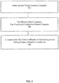
FIG. 4 depicts a representative common connection assembly, such as a bus bar, in operation in accordance with various embodiments. - The detailed description of exemplary embodiments herein makes reference to the accompanying drawings, which show exemplary embodiments by way of illustration and their best mode. While these exemplary embodiments are described in sufficient detail to enable those skilled in the art to practice the disclosure, it should be understood that other embodiments may be realized and that logical changes may be made without departing from the scope of the disclosure. Thus, the detailed description herein is presented for purposes of illustration only and not of limitation. For example, the steps recited in any of the method or process descriptions may be executed in any order and are not necessarily limited to the order presented. Furthermore, any reference to singular includes plural embodiments, and any reference to more than one component or step may include a singular embodiment or step.
- Removing heat from a device in a direct and efficient fashion is desirable. In order to circumvent traditional thermal expansion, conventionally, multiple layers of material are added to account for the thermal expansion of the electrical components and in particular the thermal expansion of a bus bar. Stated another way, in general, thermal interfaces are needed for each layer of a circuit board. Multiple thermal interfaces, such as thermal interfaces between bus work and a circuit board, may result in the part running at an elevated temperature during normal operation. This may result is a shortened lifespan of the circuit board. By removing these additional interfaces, a more efficient throughput of heat delivery to a cooling medium is achieved.
- Electrical conductivity, thermal conductivity and mechanical strength are all power distribution design considerations. Matching and/or having within an acceptable range of thermal expansion of parts in a power distribution component may also be an important design consideration.
- Traditionally, multi-interfaces between a silicon die and a conductive path exist. One of these interfaces is within the bus bar itself. One or more layers of solder, and potentially a layer of copper, and/or a layer of molybdenum may be part of a system. The thermal expansion properties of molybdenum closely match that of silicon. In response to the presence of heat, a cylindrical structure of molybdenum expands axially rather than radially. For instance, in the case of a stacked silicon die on top of a molybdenum plate, the molybdenum will expand within the plane of the plate rather than expand in a plane orthogonal to the plate. Thus, the management of the thermal expansion or the mismatch in thermal expansion between all these different components is managed through multiple layers. A bus bar with little to no thermal expansion allows for the removal of several of these interfaces. Applying conductive adhesives solders may elevate the temperatures of the devices and the entire assembly to an undesirable level.
- In accordance with various embodiments and with reference to
FIGS. 1 and2 , abus bar 100 is disclosed. At least a portion ofbus bar 100 is formed from a plurality of materials. For instance, a first portion ofbus bar 100 may be formed from a traditional bus bar material, such as brass, nickel, silver, gold, zinc, iron, copper or aluminum. A second portion ofbus bar 100 may be formed from a memory metal, shape alloy or smart metal. For instance, the memory metal may be a shape memory alloy, such as nitinol wire (nickel titanium alloy). Nitinol is a nickel-titanium alloy distinguished from other materials by its shape memory and super-elastic characteristics. Shape memory alloys are able to show an elastic deformation behavior. A super-elastic characteristic may be referred to as a mechanical shape memory effect or super elasticity. Super-elasticity is caused by the stress-induced phase transformation from a high temperature phase into a low temperature phase. The strain related to this phase transformation is fully reversible after removing the stress. - The first and second portions preferably overlap and/or form a merged structure. According to various embodiments,
bus bar 100 may be formed from an aluminum matrix with nitinol wires embedded into this matrix.Bus bar 100 may be designed and/or scaled to carry any desired voltage or power. - For instance, nitinol wire, a shape memory alloy, may be embedded using additive manufacturing in an aluminum bus bar that has high temperature silicon dies coupled to a surface, such as its top surface. Solder pads, such as a copper solder pad and/or conductive traces may also be additively manufactured on a surface, such as a top surface, of the bus bar for die attach points. This layout may be configured to provide adequate solderability for a device coupled to a surface of the device. Direct write additive manufacturing technologies may be used to form the wire bonds from the silicon/silicon carbide die to the bus bar. An exothermic soldering process using an amorphous material (Nanofoil) clad on both sides with solder material may be used to bond a silicon/silicon carbide dies to the bus bar die attach points.
- The
additive manufacturing technique 101 may include ultrasonic consolidation (or ultrasonic additive manufacturing), cold spray and/or the like. For instance, the term "cold spray" as used herein may include a process by whichparticulates 160 are deposited by means of ballistic impingement upon asuitable substrate 180 at supersonic velocities to form acoating 170 or a free-standing structure. The ballistic impingement may be via asupersonic nozzle 150. Theparticles 160 may be fed byfeeder system 130 which may toggle between various source material stocks. Also, pressure and heat may be provided by thefeeder system 130. The melting of particles that occurs during most thermal spray processes can result in oxidation of both the coating and substrate materials. The resulting oxides decrease the adhesive and cohesive strengths of the coating. The cold spray process may avoid such reactions. Cold spay process may be highly precise if desired allowing for materials to be formed in particular patterns and orientations. - According to various embodiments and with reference to
FIG. 2 , arepresentative bus bar 100assembly 200 is depicted.Nitinol wire 210 elements may be arranged in predetermined orientations, such as arranged along a common plane with spaces between thenitinol wire 210 to formsubstrate 180. Layers of material, such as aluminum, may be added, tosubstrate 180 such as through anadditive manufacturing technique 101. Layers adding thickness may be added in any direction ofbus bar 100.Copper 250, such as a portion or layer ofcopper 250 may be added to a top surface or bottom surface ofbus bar 100. The layer ofcopper 250 may be formed through anadditive manufacturing technique 101.Insulation 260 layers may be formed onbus bar 100 where desired.Insulation 260 may be made from any desired material. Theinsulation 260 is configured to electrically shield the interface between two or more components.Insulation 260 layers may be direct write insulation layers formed through theadditive manufacturing technique 101 described above. Similarly, abond wire 220 may be coupled tobus bar 100 via a direct write technique, such as throughadditive manufacturing technique 101. A mosfet die 240, such as silicon carbide die, may be bonded to thecopper layer 250 via an exothermic soldering process. For instance, dies 240 prewet with solder may be combined with a nanofoil material to join thedie 240 tobus bar 100 and/or a solder platednanofoil 230 material may be positioned between the die 240 and thecopper 250 layer. The solder platednanofoil 230 may be ignited which propagates a reaction across its surface creating a bond between the die 240 andbus bar 100. Thecomponents - According to various embodiments and with reference to
FIG. 3 , a structure of nitinol may be arranged to form a skeleton,e.g. substrate 180, to which anadditive manufacturing 101 layer or layers 170 may be added (step 310). For instance, a cold spray ofparticles 160 may be applied to a mesh like structure of nitinol wire (step 320). The orientation of the framework may be deliberate based on the thermal expansion characteristics of the framework elements. The thickness of this structure may be increased as desired by addingadditional layers 170 of both the nitinol wire framework and cold spray material. In response to a suitable quantity of layers being applied, abus bar 100 may be formed (step 350). - With continued reference to
FIG. 3 , pads and/or traces may be directly added via an additive manufacturing technique tobus bar 100, such as to a surface of bus bar 100 (step 340). Adding pads and/or traces directly to the bus bar eliminates unnecessary thermal interfaces. Utilizing the techniques and designs described herein also significantly improve the manufacturability as well as the survivability of the product/assembly over the life of the product. According to various embodiments, exothermic material may be used to bond a silicon/silicon carbide dies tobus bar 100 die attach points (step 330). - In accordance with various embodiments,
bus bar 100, connection/attach points, and various attributes may also be formed by ultrasonic additive manufacturing where the memory metal is embedded into a metal matrix created by the successive addition of material, such as a metal foil. Thus, in this process, a partial substrate may be formed to which memory metal is embedded into. Additional additive manufacturing layers of any material composition may be added to this structure if desired. - Aluminum, being an isotropic material, will thermally expand substantially equally in all directions. The orientation of the memory metal and/or the memory metal mesh may be designed to exploit contraction in the longitudinal direction (e.g. parallel with the wire or in the direction of the wire). Thus, the effects of thermal expansion on the combination of the two materials may be substantially balanced. A uniform aggregate coefficient of friction is experienced by the bus bar in response to a load being applied.
- With continued reference to
FIG. 4 , in operation (e.g. in response to delivering current through the common connection (bus bar 100), the nitinol wires contract while the aluminum expands during temperature elevation due to thermal expansion. (step 410, 420). For instance, as the temperature goes up inbus bar 100, by virtue of current running through the bus bar, the nitinol material will experience a phase change and is configured to contract while the aluminum matrix expands. The result is bus bar having reduced thermal expansion, which can be net zero coefficient of thermal expansion (step 430). Stated another way the composition of the memory metal and the electrically conductive material comprise a substantially net zero coefficient of thermal expansion during operation. The volume percent of traditional bus bar material to memory metal may be any volume percent. For instance, the relationship may be about 50 traditional bus bar material to about 50 percent memory metal. According to various embodiments, the relationship may be between about 40-90 percent memory metal to a respective amount of traditional bus bar material. - Though they may span a multitude of applicable applications, the concepts described herein may be utilized in a power distribution system. The system may be configured for and designed to address aircraft power distribution loads. According to various embodiments, the system is configured for driving motors.
- The application may be implemented as a distribution panel and/or element of a distribution panel, which is a matrix of multiple function blocks. This results in a configurable, on-demand expandable system. By using separate function blocks, and/or portions of function blocks, each functional block of the matrix may accomplish a one or more functions, and/or deliver current to more than one system. For instance, to satisfy multiple power requirements, various paths of parallel multiples of the function blocks may be aggregated to satisfy a desired power requirement.
- Benefits, other advantages, and solutions to problems have been described herein with regard to specific embodiments. Furthermore, the connecting lines shown in the various figures contained herein are intended to represent exemplary functional relationships and/or physical couplings between the various elements. It should be noted that many alternative or additional functional relationships or physical connections may be present in a practical system. However, the benefits, advantages, solutions to problems, and any elements that may cause any benefit, advantage, or solution to occur or become more pronounced are not to be construed as critical, required, or essential features or elements of the disclosure. The scope of the disclosure is accordingly to be limited by nothing other than the appended claims, in which reference to an element in the singular is not intended to mean "one and only one" unless explicitly so stated, but rather "one or more." As used herein, the phrases "make contact with", "touch", "interface with" and "engage" may be used interchangeably.
- Systems, methods and apparatus are provided herein. In the detailed description herein, references to "various embodiments", "one embodiment", "an embodiment", "an example embodiment", etc., indicate that the embodiment described may include a particular feature, structure, or characteristic, but every embodiment may not necessarily include the particular feature, structure, or characteristic. Moreover, such phrases are not necessarily referring to the same embodiment. Further, when a particular feature, structure, or characteristic is described in connection with an embodiment, it is submitted that it is within the knowledge of one skilled in the art to affect such feature, structure, or characteristic in connection with other embodiments whether or not explicitly described. After reading the description, it will be apparent to one skilled in the relevant art(s) how to implement the disclosure in alternative embodiments. Different cross-hatching is used throughout the figures to denote different parts but not necessarily to denote the same or different materials.
- Furthermore, no element, component, or method step in the present disclosure is intended to be dedicated to the public regardless of whether the element, component, or method step is explicitly recited in the claims. No claim element herein is to be construed under the provisions of 35 U.S.C. 112(f), unless the element is expressly recited using the phrase "means for." As used herein, the terms "comprises", "comprising", or any other variation thereof, are intended to cover a non-exclusive inclusion, such that a process, method, article, or apparatus that comprises a list of elements does not include only those elements but may include other elements not expressly listed or inherent to such process, method, article, or apparatus.
Claims (15)
- An electrical distribution system comprising:a power source input; anda common connection between a plurality of components,wherein the power source input is electrically coupled to the plurality of components via the common connection,wherein the common connection is formed by additive manufacturing an electrically conductive material onto a memory metal substrate framework.
- The electrical distribution system of claim 1, wherein the common connection experiences a substantially net zero coefficient of thermal expansion in response to current being delivered via the common connection.
- The electrical distribution system of claim 1 or 2, wherein the additive manufacturing technique (101) comprises a ballistic impingement at substantially supersonic velocities to form a layer of coating.
- The electrical distribution system of claim 1, 2 or 3, wherein the electrically conductive material is at least one of brass, nickel, silver, zinc, iron, copper and aluminum.
- The electrical distribution system of any of claims 1 to 4, wherein the memory metal substrate framework is a nickel-titanium alloy.
- The electrical distribution system of any of claims 1 to 5, further comprising at least one of a solder pad and a conductive trace, wherein the at least one of the solder pad and the conductive trace are formed through an additive manufacturing technique (101).
- The electrical distribution system of any of claims 1 to 6, further comprising a silicon carbide die (240) bonded to a common connection die attach location, wherein the bond is made via an exothermic soldering process.
- A bus bar (100) comprising:a memory metal internal framework; andan electrically conductive material applied to the memory metal internal framework through an additive manufacturing technique (101),wherein the composition of the memory metal internal framework and the electrically conductive material comprise a substantially net zero coefficient of thermal expansion during operation of the bus bar (100).
- The bus bar of claim 8, wherein the additive manufacturing technique (101) is at least one of ultrasonic disposition and cold spraying.
- The bus bar of claim 8 or 9, wherein the electrically conductive material is at least one of brass, nickel, silver, gold, zinc, iron, copper and aluminum.
- The bus bar of claim 8, 9 or 10, wherein the memory metal internal framework is a nickel-titanium alloy.
- The bus bar of any of claims 8 to 11, further comprising at least one of a solder pad and a conductive trace formed on a surface of the bus bar (100), wherein at least one of the solder pad and the conductive trace are formed through an additive manufacturing technique (101).
- The bus bar of any of claims 8 to 12, further comprising a silicon carbide die (240) bonded to a bus bar die attachment location, wherein the bond is made via an exothermic soldering process.
- The bus bar of any of claims 8 to 13, wherein the additive manufacturing technique (101) comprises a ballistic impingement at substantially supersonic velocities to form a layer (170) of coating.
- The bus bar of any of claims 8 to 14, wherein the bus bar (100) is a function block element of a power distribution system, wherein parallel multiples of the function blocks are aggregated as needed to satisfy a desired power requirement.
Applications Claiming Priority (3)
| Application Number | Priority Date | Filing Date | Title |
|---|---|---|---|
| US201361888937P | 2013-10-09 | 2013-10-09 | |
| US14/162,332 US9691515B2 (en) | 2013-10-09 | 2014-01-23 | Bus bar assembly comprising a memory metal composition |
| EP14187911.4A EP2860737B1 (en) | 2013-10-09 | 2014-10-07 | Bus bar assembly comprising a memory metal composition |
Related Parent Applications (2)
| Application Number | Title | Priority Date | Filing Date |
|---|---|---|---|
| EP14187911.4A Division EP2860737B1 (en) | 2013-10-09 | 2014-10-07 | Bus bar assembly comprising a memory metal composition |
| EP14187911.4A Division-Into EP2860737B1 (en) | 2013-10-09 | 2014-10-07 | Bus bar assembly comprising a memory metal composition |
Publications (2)
| Publication Number | Publication Date |
|---|---|
| EP3288039A1 true EP3288039A1 (en) | 2018-02-28 |
| EP3288039B1 EP3288039B1 (en) | 2020-04-01 |
Family
ID=51730344
Family Applications (2)
| Application Number | Title | Priority Date | Filing Date |
|---|---|---|---|
| EP17186503.3A Active EP3288039B1 (en) | 2013-10-09 | 2014-10-07 | Bus bar assembly comprising a memory metal composition |
| EP14187911.4A Active EP2860737B1 (en) | 2013-10-09 | 2014-10-07 | Bus bar assembly comprising a memory metal composition |
Family Applications After (1)
| Application Number | Title | Priority Date | Filing Date |
|---|---|---|---|
| EP14187911.4A Active EP2860737B1 (en) | 2013-10-09 | 2014-10-07 | Bus bar assembly comprising a memory metal composition |
Country Status (2)
| Country | Link |
|---|---|
| US (1) | US9691515B2 (en) |
| EP (2) | EP3288039B1 (en) |
Families Citing this family (8)
| Publication number | Priority date | Publication date | Assignee | Title |
|---|---|---|---|---|
| US12560846B2 (en) | 2010-11-08 | 2026-02-24 | View Operating Corporation | Adhesive bus bars in electrochromic windows |
| US10884311B2 (en) | 2013-12-24 | 2021-01-05 | View, Inc. | Obscuring bus bars in electrochromic glass structures |
| US11906868B2 (en) | 2013-12-24 | 2024-02-20 | View, Inc. | Obscuring bus bars in electrochromic glass structures |
| EP3907368A1 (en) | 2013-12-24 | 2021-11-10 | View, Inc. | Obscuring bus bars in electrochromic glass structures |
| US9431330B2 (en) * | 2014-08-07 | 2016-08-30 | Hamilton Sundstrand Corporation | System and method for metal matrix mounting scheme |
| WO2017156157A1 (en) * | 2016-03-09 | 2017-09-14 | View, Inc. | Metal accretion bus bars |
| FR3082368B1 (en) * | 2018-06-08 | 2022-02-04 | Schneider Electric Ind Sas | PROTECTION BOX FOR AN ELECTRICAL INSTALLATION AND ELECTRICAL INSTALLATION COMPRISING SUCH A PROTECTION BOX |
| DK182176B1 (en) * | 2023-03-28 | 2025-10-15 | Kk Wind Solutions As | Electrical local connecting busbar |
Citations (3)
| Publication number | Priority date | Publication date | Assignee | Title |
|---|---|---|---|---|
| EP2355638A2 (en) * | 2010-02-02 | 2011-08-10 | Hamilton Sundstrand Corporation | Bus bar assembly |
| CN102501006A (en) * | 2011-10-26 | 2012-06-20 | 西安交通大学 | Method for manufacturing shape memory alloy-aluminum metal matrix composite material through ultrasonic welding |
| US20130127690A1 (en) * | 2011-11-18 | 2013-05-23 | Industrial Technology Research Institute | Electronic apparatus and display apparatus |
Family Cites Families (9)
| Publication number | Priority date | Publication date | Assignee | Title |
|---|---|---|---|---|
| US5981085A (en) | 1996-03-21 | 1999-11-09 | The Furukawa Electric Co., Inc. | Composite substrate for heat-generating semiconductor device and semiconductor apparatus using the same |
| US20060164813A1 (en) * | 2004-11-30 | 2006-07-27 | Kabushiki Kaisha Toshiba | Semiconductor package and semiconductor module |
| NZ547608A (en) * | 2006-05-31 | 2008-11-28 | Waikatolink Ltd | Method for producing titanium metal alloy and intermetallic powders |
| KR20080010086A (en) * | 2006-07-26 | 2008-01-30 | (주)태광테크 | Busbar manufacturing method using low temperature spray coating |
| US20090200864A1 (en) * | 2008-02-12 | 2009-08-13 | Josef Maier | Chip on bus bar |
| DE102010051669A1 (en) | 2010-11-17 | 2012-05-24 | Li-Tec Battery Gmbh | Electrical component |
| US8469724B1 (en) * | 2011-12-30 | 2013-06-25 | International Business Machines Corporation | Bus bar for power distribution on a printed circuit board |
| CN102534275B (en) * | 2012-01-09 | 2013-10-30 | 华南理工大学 | TiNi alloy-based composite material with near-zero thermal expansion characteristic and preparation method thereof |
| CN102832377A (en) | 2012-08-17 | 2012-12-19 | 华南理工大学 | Tin-amorphous nickel titanium composite film cathode material and preparation method and application thereof |
-
2014
- 2014-01-23 US US14/162,332 patent/US9691515B2/en active Active
- 2014-10-07 EP EP17186503.3A patent/EP3288039B1/en active Active
- 2014-10-07 EP EP14187911.4A patent/EP2860737B1/en active Active
Patent Citations (3)
| Publication number | Priority date | Publication date | Assignee | Title |
|---|---|---|---|---|
| EP2355638A2 (en) * | 2010-02-02 | 2011-08-10 | Hamilton Sundstrand Corporation | Bus bar assembly |
| CN102501006A (en) * | 2011-10-26 | 2012-06-20 | 西安交通大学 | Method for manufacturing shape memory alloy-aluminum metal matrix composite material through ultrasonic welding |
| US20130127690A1 (en) * | 2011-11-18 | 2013-05-23 | Industrial Technology Research Institute | Electronic apparatus and display apparatus |
Also Published As
| Publication number | Publication date |
|---|---|
| EP2860737B1 (en) | 2017-12-06 |
| US20150098169A1 (en) | 2015-04-09 |
| US9691515B2 (en) | 2017-06-27 |
| EP3288039B1 (en) | 2020-04-01 |
| EP2860737A3 (en) | 2015-08-05 |
| EP2860737A2 (en) | 2015-04-15 |
Similar Documents
| Publication | Publication Date | Title |
|---|---|---|
| US9691515B2 (en) | Bus bar assembly comprising a memory metal composition | |
| CN107210282B (en) | Electronic package including multilayer stiffener | |
| JP6132014B2 (en) | Semiconductor device and manufacturing method of semiconductor device | |
| McCluskey | Reliability of power electronics under thermal loading | |
| JP6029222B1 (en) | Metal particles, paste, molded body, and laminate | |
| JPWO2020071036A1 (en) | Thermoelectric conversion module and cooling device or temperature measuring device using it or heat flow sensor or power generation device | |
| US12208448B2 (en) | Transient liquid phase bonding compositions and power electronics assemblies incorporating the same | |
| JP7499869B2 (en) | Connecting the parts | |
| EP2892310A2 (en) | Heat sink for contactor in power distribution assembly | |
| KR100992961B1 (en) | Heat exchanger in plate type | |
| JP2017524248A (en) | COOLING DEVICE, COOLING DEVICE MANUFACTURING METHOD, AND POWER CIRCUIT | |
| Boettge et al. | Packaging material issues in high temperature power electronics | |
| CN205305224U (en) | Flexible circuit board | |
| JP2011192686A (en) | Semiconductor device | |
| JP5415525B2 (en) | Electrical bonding connection structure | |
| EP2983200B1 (en) | System and method for metal matrix mounting scheme | |
| JP2006278558A (en) | Insulated heat transfer structure and power module substrate | |
| JP2016219681A (en) | Structure and method for joining metal wiring | |
| JP5106420B2 (en) | Electronic module and method for assembling such a module | |
| CN105762270B (en) | Thermoelectric generator and method of assembling thermoelectric generator | |
| JP4407521B2 (en) | Insulated heat transfer structure and power module substrate | |
| JP2011061105A (en) | Connection structure, power module, and method of manufacturing the same | |
| JP2006269572A (en) | Thermoelectric conversion module, circuit board, and method of manufacturing thermoelectric conversion module | |
| JP2013072093A (en) | Connection structure between different kinds of metal members | |
| CN106133896B (en) | Semiconductor module |
Legal Events
| Date | Code | Title | Description |
|---|---|---|---|
| PUAI | Public reference made under article 153(3) epc to a published international application that has entered the european phase |
Free format text: ORIGINAL CODE: 0009012 |
|
| STAA | Information on the status of an ep patent application or granted ep patent |
Free format text: STATUS: THE APPLICATION HAS BEEN PUBLISHED |
|
| AC | Divisional application: reference to earlier application |
Ref document number: 2860737 Country of ref document: EP Kind code of ref document: P |
|
| AK | Designated contracting states |
Kind code of ref document: A1 Designated state(s): AL AT BE BG CH CY CZ DE DK EE ES FI FR GB GR HR HU IE IS IT LI LT LU LV MC MK MT NL NO PL PT RO RS SE SI SK SM TR |
|
| STAA | Information on the status of an ep patent application or granted ep patent |
Free format text: STATUS: REQUEST FOR EXAMINATION WAS MADE |
|
| 17P | Request for examination filed |
Effective date: 20180828 |
|
| RBV | Designated contracting states (corrected) |
Designated state(s): AL AT BE BG CH CY CZ DE DK EE ES FI FR GB GR HR HU IE IS IT LI LT LU LV MC MK MT NL NO PL PT RO RS SE SI SK SM TR |
|
| STAA | Information on the status of an ep patent application or granted ep patent |
Free format text: STATUS: EXAMINATION IS IN PROGRESS |
|
| 17Q | First examination report despatched |
Effective date: 20190211 |
|
| GRAP | Despatch of communication of intention to grant a patent |
Free format text: ORIGINAL CODE: EPIDOSNIGR1 |
|
| STAA | Information on the status of an ep patent application or granted ep patent |
Free format text: STATUS: GRANT OF PATENT IS INTENDED |
|
| INTG | Intention to grant announced |
Effective date: 20191011 |
|
| GRAS | Grant fee paid |
Free format text: ORIGINAL CODE: EPIDOSNIGR3 |
|
| GRAA | (expected) grant |
Free format text: ORIGINAL CODE: 0009210 |
|
| STAA | Information on the status of an ep patent application or granted ep patent |
Free format text: STATUS: THE PATENT HAS BEEN GRANTED |
|
| AC | Divisional application: reference to earlier application |
Ref document number: 2860737 Country of ref document: EP Kind code of ref document: P |
|
| AK | Designated contracting states |
Kind code of ref document: B1 Designated state(s): AL AT BE BG CH CY CZ DE DK EE ES FI FR GB GR HR HU IE IS IT LI LT LU LV MC MK MT NL NO PL PT RO RS SE SI SK SM TR |
|
| REG | Reference to a national code |
Ref country code: GB Ref legal event code: FG4D |
|
| REG | Reference to a national code |
Ref country code: CH Ref legal event code: EP Ref country code: AT Ref legal event code: REF Ref document number: 1252432 Country of ref document: AT Kind code of ref document: T Effective date: 20200415 |
|
| REG | Reference to a national code |
Ref country code: DE Ref legal event code: R096 Ref document number: 602014063361 Country of ref document: DE |
|
| REG | Reference to a national code |
Ref country code: IE Ref legal event code: FG4D |
|
| PG25 | Lapsed in a contracting state [announced via postgrant information from national office to epo] |
Ref country code: BG Free format text: LAPSE BECAUSE OF FAILURE TO SUBMIT A TRANSLATION OF THE DESCRIPTION OR TO PAY THE FEE WITHIN THE PRESCRIBED TIME-LIMIT Effective date: 20200701 |
|
| REG | Reference to a national code |
Ref country code: NL Ref legal event code: MP Effective date: 20200401 |
|
| REG | Reference to a national code |
Ref country code: LT Ref legal event code: MG4D |
|
| PG25 | Lapsed in a contracting state [announced via postgrant information from national office to epo] |
Ref country code: IS Free format text: LAPSE BECAUSE OF FAILURE TO SUBMIT A TRANSLATION OF THE DESCRIPTION OR TO PAY THE FEE WITHIN THE PRESCRIBED TIME-LIMIT Effective date: 20200801 Ref country code: NO Free format text: LAPSE BECAUSE OF FAILURE TO SUBMIT A TRANSLATION OF THE DESCRIPTION OR TO PAY THE FEE WITHIN THE PRESCRIBED TIME-LIMIT Effective date: 20200701 Ref country code: GR Free format text: LAPSE BECAUSE OF FAILURE TO SUBMIT A TRANSLATION OF THE DESCRIPTION OR TO PAY THE FEE WITHIN THE PRESCRIBED TIME-LIMIT Effective date: 20200702 Ref country code: PT Free format text: LAPSE BECAUSE OF FAILURE TO SUBMIT A TRANSLATION OF THE DESCRIPTION OR TO PAY THE FEE WITHIN THE PRESCRIBED TIME-LIMIT Effective date: 20200817 Ref country code: CZ Free format text: LAPSE BECAUSE OF FAILURE TO SUBMIT A TRANSLATION OF THE DESCRIPTION OR TO PAY THE FEE WITHIN THE PRESCRIBED TIME-LIMIT Effective date: 20200401 Ref country code: NL Free format text: LAPSE BECAUSE OF FAILURE TO SUBMIT A TRANSLATION OF THE DESCRIPTION OR TO PAY THE FEE WITHIN THE PRESCRIBED TIME-LIMIT Effective date: 20200401 Ref country code: LT Free format text: LAPSE BECAUSE OF FAILURE TO SUBMIT A TRANSLATION OF THE DESCRIPTION OR TO PAY THE FEE WITHIN THE PRESCRIBED TIME-LIMIT Effective date: 20200401 Ref country code: SE Free format text: LAPSE BECAUSE OF FAILURE TO SUBMIT A TRANSLATION OF THE DESCRIPTION OR TO PAY THE FEE WITHIN THE PRESCRIBED TIME-LIMIT Effective date: 20200401 Ref country code: FI Free format text: LAPSE BECAUSE OF FAILURE TO SUBMIT A TRANSLATION OF THE DESCRIPTION OR TO PAY THE FEE WITHIN THE PRESCRIBED TIME-LIMIT Effective date: 20200401 |
|
| REG | Reference to a national code |
Ref country code: AT Ref legal event code: MK05 Ref document number: 1252432 Country of ref document: AT Kind code of ref document: T Effective date: 20200401 |
|
| PG25 | Lapsed in a contracting state [announced via postgrant information from national office to epo] |
Ref country code: HR Free format text: LAPSE BECAUSE OF FAILURE TO SUBMIT A TRANSLATION OF THE DESCRIPTION OR TO PAY THE FEE WITHIN THE PRESCRIBED TIME-LIMIT Effective date: 20200401 Ref country code: LV Free format text: LAPSE BECAUSE OF FAILURE TO SUBMIT A TRANSLATION OF THE DESCRIPTION OR TO PAY THE FEE WITHIN THE PRESCRIBED TIME-LIMIT Effective date: 20200401 Ref country code: RS Free format text: LAPSE BECAUSE OF FAILURE TO SUBMIT A TRANSLATION OF THE DESCRIPTION OR TO PAY THE FEE WITHIN THE PRESCRIBED TIME-LIMIT Effective date: 20200401 |
|
| PG25 | Lapsed in a contracting state [announced via postgrant information from national office to epo] |
Ref country code: AL Free format text: LAPSE BECAUSE OF FAILURE TO SUBMIT A TRANSLATION OF THE DESCRIPTION OR TO PAY THE FEE WITHIN THE PRESCRIBED TIME-LIMIT Effective date: 20200401 |
|
| REG | Reference to a national code |
Ref country code: DE Ref legal event code: R097 Ref document number: 602014063361 Country of ref document: DE |
|
| PG25 | Lapsed in a contracting state [announced via postgrant information from national office to epo] |
Ref country code: AT Free format text: LAPSE BECAUSE OF FAILURE TO SUBMIT A TRANSLATION OF THE DESCRIPTION OR TO PAY THE FEE WITHIN THE PRESCRIBED TIME-LIMIT Effective date: 20200401 Ref country code: ES Free format text: LAPSE BECAUSE OF FAILURE TO SUBMIT A TRANSLATION OF THE DESCRIPTION OR TO PAY THE FEE WITHIN THE PRESCRIBED TIME-LIMIT Effective date: 20200401 Ref country code: RO Free format text: LAPSE BECAUSE OF FAILURE TO SUBMIT A TRANSLATION OF THE DESCRIPTION OR TO PAY THE FEE WITHIN THE PRESCRIBED TIME-LIMIT Effective date: 20200401 Ref country code: IT Free format text: LAPSE BECAUSE OF FAILURE TO SUBMIT A TRANSLATION OF THE DESCRIPTION OR TO PAY THE FEE WITHIN THE PRESCRIBED TIME-LIMIT Effective date: 20200401 Ref country code: EE Free format text: LAPSE BECAUSE OF FAILURE TO SUBMIT A TRANSLATION OF THE DESCRIPTION OR TO PAY THE FEE WITHIN THE PRESCRIBED TIME-LIMIT Effective date: 20200401 Ref country code: SM Free format text: LAPSE BECAUSE OF FAILURE TO SUBMIT A TRANSLATION OF THE DESCRIPTION OR TO PAY THE FEE WITHIN THE PRESCRIBED TIME-LIMIT Effective date: 20200401 Ref country code: DK Free format text: LAPSE BECAUSE OF FAILURE TO SUBMIT A TRANSLATION OF THE DESCRIPTION OR TO PAY THE FEE WITHIN THE PRESCRIBED TIME-LIMIT Effective date: 20200401 |
|
| PLBE | No opposition filed within time limit |
Free format text: ORIGINAL CODE: 0009261 |
|
| STAA | Information on the status of an ep patent application or granted ep patent |
Free format text: STATUS: NO OPPOSITION FILED WITHIN TIME LIMIT |
|
| PG25 | Lapsed in a contracting state [announced via postgrant information from national office to epo] |
Ref country code: SK Free format text: LAPSE BECAUSE OF FAILURE TO SUBMIT A TRANSLATION OF THE DESCRIPTION OR TO PAY THE FEE WITHIN THE PRESCRIBED TIME-LIMIT Effective date: 20200401 Ref country code: PL Free format text: LAPSE BECAUSE OF FAILURE TO SUBMIT A TRANSLATION OF THE DESCRIPTION OR TO PAY THE FEE WITHIN THE PRESCRIBED TIME-LIMIT Effective date: 20200401 |
|
| 26N | No opposition filed |
Effective date: 20210112 |
|
| PG25 | Lapsed in a contracting state [announced via postgrant information from national office to epo] |
Ref country code: SI Free format text: LAPSE BECAUSE OF FAILURE TO SUBMIT A TRANSLATION OF THE DESCRIPTION OR TO PAY THE FEE WITHIN THE PRESCRIBED TIME-LIMIT Effective date: 20200401 |
|
| REG | Reference to a national code |
Ref country code: CH Ref legal event code: PL |
|
| PG25 | Lapsed in a contracting state [announced via postgrant information from national office to epo] |
Ref country code: MC Free format text: LAPSE BECAUSE OF FAILURE TO SUBMIT A TRANSLATION OF THE DESCRIPTION OR TO PAY THE FEE WITHIN THE PRESCRIBED TIME-LIMIT Effective date: 20200401 Ref country code: LU Free format text: LAPSE BECAUSE OF NON-PAYMENT OF DUE FEES Effective date: 20201007 |
|
| REG | Reference to a national code |
Ref country code: BE Ref legal event code: MM Effective date: 20201031 |
|
| PG25 | Lapsed in a contracting state [announced via postgrant information from national office to epo] |
Ref country code: LI Free format text: LAPSE BECAUSE OF NON-PAYMENT OF DUE FEES Effective date: 20201031 Ref country code: BE Free format text: LAPSE BECAUSE OF NON-PAYMENT OF DUE FEES Effective date: 20201031 Ref country code: CH Free format text: LAPSE BECAUSE OF NON-PAYMENT OF DUE FEES Effective date: 20201031 |
|
| PG25 | Lapsed in a contracting state [announced via postgrant information from national office to epo] |
Ref country code: IE Free format text: LAPSE BECAUSE OF NON-PAYMENT OF DUE FEES Effective date: 20201007 |
|
| PG25 | Lapsed in a contracting state [announced via postgrant information from national office to epo] |
Ref country code: TR Free format text: LAPSE BECAUSE OF FAILURE TO SUBMIT A TRANSLATION OF THE DESCRIPTION OR TO PAY THE FEE WITHIN THE PRESCRIBED TIME-LIMIT Effective date: 20200401 Ref country code: MT Free format text: LAPSE BECAUSE OF FAILURE TO SUBMIT A TRANSLATION OF THE DESCRIPTION OR TO PAY THE FEE WITHIN THE PRESCRIBED TIME-LIMIT Effective date: 20200401 Ref country code: CY Free format text: LAPSE BECAUSE OF FAILURE TO SUBMIT A TRANSLATION OF THE DESCRIPTION OR TO PAY THE FEE WITHIN THE PRESCRIBED TIME-LIMIT Effective date: 20200401 |
|
| PG25 | Lapsed in a contracting state [announced via postgrant information from national office to epo] |
Ref country code: MK Free format text: LAPSE BECAUSE OF FAILURE TO SUBMIT A TRANSLATION OF THE DESCRIPTION OR TO PAY THE FEE WITHIN THE PRESCRIBED TIME-LIMIT Effective date: 20200401 |
|
| P01 | Opt-out of the competence of the unified patent court (upc) registered |
Effective date: 20230522 |
|
| PGFP | Annual fee paid to national office [announced via postgrant information from national office to epo] |
Ref country code: GB Payment date: 20250923 Year of fee payment: 12 |
|
| PGFP | Annual fee paid to national office [announced via postgrant information from national office to epo] |
Ref country code: FR Payment date: 20250923 Year of fee payment: 12 |
|
| PGFP | Annual fee paid to national office [announced via postgrant information from national office to epo] |
Ref country code: DE Payment date: 20250923 Year of fee payment: 12 |