EP3285298A1 - Electrostatic discharge protection structure and fabricating method thereof - Google Patents
Electrostatic discharge protection structure and fabricating method thereof Download PDFInfo
- Publication number
- EP3285298A1 EP3285298A1 EP17185877.2A EP17185877A EP3285298A1 EP 3285298 A1 EP3285298 A1 EP 3285298A1 EP 17185877 A EP17185877 A EP 17185877A EP 3285298 A1 EP3285298 A1 EP 3285298A1
- Authority
- EP
- European Patent Office
- Prior art keywords
- region
- substrate
- doped layer
- fin portion
- electrostatic discharge
- Prior art date
- Legal status (The legal status is an assumption and is not a legal conclusion. Google has not performed a legal analysis and makes no representation as to the accuracy of the status listed.)
- Withdrawn
Links
- 238000000034 method Methods 0.000 title claims description 79
- 239000000758 substrate Substances 0.000 claims abstract description 175
- 238000002955 isolation Methods 0.000 claims description 80
- 238000005530 etching Methods 0.000 claims description 23
- 230000017525 heat dissipation Effects 0.000 abstract description 18
- 150000002500 ions Chemical class 0.000 description 41
- 239000002019 doping agent Substances 0.000 description 33
- 239000004065 semiconductor Substances 0.000 description 19
- 239000000463 material Substances 0.000 description 15
- -1 phosphorus ions Chemical class 0.000 description 15
- 230000001965 increasing effect Effects 0.000 description 12
- XUIMIQQOPSSXEZ-UHFFFAOYSA-N Silicon Chemical compound [Si] XUIMIQQOPSSXEZ-UHFFFAOYSA-N 0.000 description 11
- 229910052710 silicon Inorganic materials 0.000 description 11
- 239000010703 silicon Substances 0.000 description 11
- 229920002120 photoresistant polymer Polymers 0.000 description 8
- 229910000577 Silicon-germanium Inorganic materials 0.000 description 6
- LEVVHYCKPQWKOP-UHFFFAOYSA-N [Si].[Ge] Chemical compound [Si].[Ge] LEVVHYCKPQWKOP-UHFFFAOYSA-N 0.000 description 6
- 238000001312 dry etching Methods 0.000 description 6
- 238000001039 wet etching Methods 0.000 description 6
- VYPSYNLAJGMNEJ-UHFFFAOYSA-N Silicium dioxide Chemical compound O=[Si]=O VYPSYNLAJGMNEJ-UHFFFAOYSA-N 0.000 description 5
- 239000006117 anti-reflective coating Substances 0.000 description 5
- 229910052785 arsenic Inorganic materials 0.000 description 5
- 230000015572 biosynthetic process Effects 0.000 description 5
- 229910052698 phosphorus Inorganic materials 0.000 description 5
- 239000011574 phosphorus Substances 0.000 description 5
- 229910052814 silicon oxide Inorganic materials 0.000 description 5
- 229910052796 boron Inorganic materials 0.000 description 4
- 238000010586 diagram Methods 0.000 description 4
- 229910052732 germanium Inorganic materials 0.000 description 4
- GNPVGFCGXDBREM-UHFFFAOYSA-N germanium atom Chemical compound [Ge] GNPVGFCGXDBREM-UHFFFAOYSA-N 0.000 description 4
- 230000002708 enhancing effect Effects 0.000 description 3
- 230000005669 field effect Effects 0.000 description 3
- 230000010354 integration Effects 0.000 description 3
- 229910052581 Si3N4 Inorganic materials 0.000 description 2
- 239000003989 dielectric material Substances 0.000 description 2
- 230000000694 effects Effects 0.000 description 2
- 238000011065 in-situ storage Methods 0.000 description 2
- 239000012212 insulator Substances 0.000 description 2
- 238000004519 manufacturing process Methods 0.000 description 2
- 229910052751 metal Inorganic materials 0.000 description 2
- 239000002184 metal Substances 0.000 description 2
- 238000012986 modification Methods 0.000 description 2
- 230000004048 modification Effects 0.000 description 2
- 229910021420 polycrystalline silicon Inorganic materials 0.000 description 2
- 229920005591 polysilicon Polymers 0.000 description 2
- HQVNEWCFYHHQES-UHFFFAOYSA-N silicon nitride Chemical compound N12[Si]34N5[Si]62N3[Si]51N64 HQVNEWCFYHHQES-UHFFFAOYSA-N 0.000 description 2
- 229910015900 BF3 Inorganic materials 0.000 description 1
- HMDDXIMCDZRSNE-UHFFFAOYSA-N [C].[Si] Chemical compound [C].[Si] HMDDXIMCDZRSNE-UHFFFAOYSA-N 0.000 description 1
- CREMABGTGYGIQB-UHFFFAOYSA-N carbon carbon Chemical compound C.C CREMABGTGYGIQB-UHFFFAOYSA-N 0.000 description 1
- 239000011203 carbon fibre reinforced carbon Substances 0.000 description 1
- 238000001816 cooling Methods 0.000 description 1
- 230000001419 dependent effect Effects 0.000 description 1
- 238000005468 ion implantation Methods 0.000 description 1
- 238000000206 photolithography Methods 0.000 description 1
- 239000000376 reactant Substances 0.000 description 1
- 239000012495 reaction gas Substances 0.000 description 1
- 230000000717 retained effect Effects 0.000 description 1
- 238000005406 washing Methods 0.000 description 1
- XLYOFNOQVPJJNP-UHFFFAOYSA-N water Substances O XLYOFNOQVPJJNP-UHFFFAOYSA-N 0.000 description 1
Images


Classifications
-
- H—ELECTRICITY
- H01—ELECTRIC ELEMENTS
- H01L—SEMICONDUCTOR DEVICES NOT COVERED BY CLASS H10
- H01L27/00—Devices consisting of a plurality of semiconductor or other solid-state components formed in or on a common substrate
- H01L27/02—Devices consisting of a plurality of semiconductor or other solid-state components formed in or on a common substrate including semiconductor components specially adapted for rectifying, oscillating, amplifying or switching and having at least one potential-jump barrier or surface barrier; including integrated passive circuit elements with at least one potential-jump barrier or surface barrier
- H01L27/0203—Particular design considerations for integrated circuits
- H01L27/0248—Particular design considerations for integrated circuits for electrical or thermal protection, e.g. electrostatic discharge [ESD] protection
- H01L27/0251—Particular design considerations for integrated circuits for electrical or thermal protection, e.g. electrostatic discharge [ESD] protection for MOS devices
- H01L27/0266—Particular design considerations for integrated circuits for electrical or thermal protection, e.g. electrostatic discharge [ESD] protection for MOS devices using field effect transistors as protective elements
-
- H—ELECTRICITY
- H01—ELECTRIC ELEMENTS
- H01L—SEMICONDUCTOR DEVICES NOT COVERED BY CLASS H10
- H01L21/00—Processes or apparatus adapted for the manufacture or treatment of semiconductor or solid state devices or of parts thereof
- H01L21/02—Manufacture or treatment of semiconductor devices or of parts thereof
- H01L21/04—Manufacture or treatment of semiconductor devices or of parts thereof the devices having at least one potential-jump barrier or surface barrier, e.g. PN junction, depletion layer or carrier concentration layer
- H01L21/18—Manufacture or treatment of semiconductor devices or of parts thereof the devices having at least one potential-jump barrier or surface barrier, e.g. PN junction, depletion layer or carrier concentration layer the devices having semiconductor bodies comprising elements of Group IV of the Periodic System or AIIIBV compounds with or without impurities, e.g. doping materials
- H01L21/30—Treatment of semiconductor bodies using processes or apparatus not provided for in groups H01L21/20 - H01L21/26
- H01L21/302—Treatment of semiconductor bodies using processes or apparatus not provided for in groups H01L21/20 - H01L21/26 to change their surface-physical characteristics or shape, e.g. etching, polishing, cutting
- H01L21/306—Chemical or electrical treatment, e.g. electrolytic etching
- H01L21/30604—Chemical etching
-
- H—ELECTRICITY
- H01—ELECTRIC ELEMENTS
- H01L—SEMICONDUCTOR DEVICES NOT COVERED BY CLASS H10
- H01L21/00—Processes or apparatus adapted for the manufacture or treatment of semiconductor or solid state devices or of parts thereof
- H01L21/02—Manufacture or treatment of semiconductor devices or of parts thereof
- H01L21/04—Manufacture or treatment of semiconductor devices or of parts thereof the devices having at least one potential-jump barrier or surface barrier, e.g. PN junction, depletion layer or carrier concentration layer
- H01L21/18—Manufacture or treatment of semiconductor devices or of parts thereof the devices having at least one potential-jump barrier or surface barrier, e.g. PN junction, depletion layer or carrier concentration layer the devices having semiconductor bodies comprising elements of Group IV of the Periodic System or AIIIBV compounds with or without impurities, e.g. doping materials
- H01L21/30—Treatment of semiconductor bodies using processes or apparatus not provided for in groups H01L21/20 - H01L21/26
- H01L21/302—Treatment of semiconductor bodies using processes or apparatus not provided for in groups H01L21/20 - H01L21/26 to change their surface-physical characteristics or shape, e.g. etching, polishing, cutting
- H01L21/306—Chemical or electrical treatment, e.g. electrolytic etching
- H01L21/308—Chemical or electrical treatment, e.g. electrolytic etching using masks
- H01L21/3081—Chemical or electrical treatment, e.g. electrolytic etching using masks characterised by their composition, e.g. multilayer masks, materials
-
- H—ELECTRICITY
- H01—ELECTRIC ELEMENTS
- H01L—SEMICONDUCTOR DEVICES NOT COVERED BY CLASS H10
- H01L21/00—Processes or apparatus adapted for the manufacture or treatment of semiconductor or solid state devices or of parts thereof
- H01L21/70—Manufacture or treatment of devices consisting of a plurality of solid state components formed in or on a common substrate or of parts thereof; Manufacture of integrated circuit devices or of parts thereof
- H01L21/77—Manufacture or treatment of devices consisting of a plurality of solid state components or integrated circuits formed in, or on, a common substrate
- H01L21/78—Manufacture or treatment of devices consisting of a plurality of solid state components or integrated circuits formed in, or on, a common substrate with subsequent division of the substrate into plural individual devices
- H01L21/82—Manufacture or treatment of devices consisting of a plurality of solid state components or integrated circuits formed in, or on, a common substrate with subsequent division of the substrate into plural individual devices to produce devices, e.g. integrated circuits, each consisting of a plurality of components
- H01L21/822—Manufacture or treatment of devices consisting of a plurality of solid state components or integrated circuits formed in, or on, a common substrate with subsequent division of the substrate into plural individual devices to produce devices, e.g. integrated circuits, each consisting of a plurality of components the substrate being a semiconductor, using silicon technology
- H01L21/8232—Field-effect technology
- H01L21/8234—MIS technology, i.e. integration processes of field effect transistors of the conductor-insulator-semiconductor type
- H01L21/823418—MIS technology, i.e. integration processes of field effect transistors of the conductor-insulator-semiconductor type with a particular manufacturing method of the source or drain structures, e.g. specific source or drain implants or silicided source or drain structures or raised source or drain structures
-
- H—ELECTRICITY
- H01—ELECTRIC ELEMENTS
- H01L—SEMICONDUCTOR DEVICES NOT COVERED BY CLASS H10
- H01L21/00—Processes or apparatus adapted for the manufacture or treatment of semiconductor or solid state devices or of parts thereof
- H01L21/70—Manufacture or treatment of devices consisting of a plurality of solid state components formed in or on a common substrate or of parts thereof; Manufacture of integrated circuit devices or of parts thereof
- H01L21/77—Manufacture or treatment of devices consisting of a plurality of solid state components or integrated circuits formed in, or on, a common substrate
- H01L21/78—Manufacture or treatment of devices consisting of a plurality of solid state components or integrated circuits formed in, or on, a common substrate with subsequent division of the substrate into plural individual devices
- H01L21/82—Manufacture or treatment of devices consisting of a plurality of solid state components or integrated circuits formed in, or on, a common substrate with subsequent division of the substrate into plural individual devices to produce devices, e.g. integrated circuits, each consisting of a plurality of components
- H01L21/822—Manufacture or treatment of devices consisting of a plurality of solid state components or integrated circuits formed in, or on, a common substrate with subsequent division of the substrate into plural individual devices to produce devices, e.g. integrated circuits, each consisting of a plurality of components the substrate being a semiconductor, using silicon technology
- H01L21/8232—Field-effect technology
- H01L21/8234—MIS technology, i.e. integration processes of field effect transistors of the conductor-insulator-semiconductor type
- H01L21/823431—MIS technology, i.e. integration processes of field effect transistors of the conductor-insulator-semiconductor type with a particular manufacturing method of transistors with a horizontal current flow in a vertical sidewall of a semiconductor body, e.g. FinFET, MuGFET
-
- H—ELECTRICITY
- H01—ELECTRIC ELEMENTS
- H01L—SEMICONDUCTOR DEVICES NOT COVERED BY CLASS H10
- H01L21/00—Processes or apparatus adapted for the manufacture or treatment of semiconductor or solid state devices or of parts thereof
- H01L21/70—Manufacture or treatment of devices consisting of a plurality of solid state components formed in or on a common substrate or of parts thereof; Manufacture of integrated circuit devices or of parts thereof
- H01L21/77—Manufacture or treatment of devices consisting of a plurality of solid state components or integrated circuits formed in, or on, a common substrate
- H01L21/78—Manufacture or treatment of devices consisting of a plurality of solid state components or integrated circuits formed in, or on, a common substrate with subsequent division of the substrate into plural individual devices
- H01L21/82—Manufacture or treatment of devices consisting of a plurality of solid state components or integrated circuits formed in, or on, a common substrate with subsequent division of the substrate into plural individual devices to produce devices, e.g. integrated circuits, each consisting of a plurality of components
- H01L21/822—Manufacture or treatment of devices consisting of a plurality of solid state components or integrated circuits formed in, or on, a common substrate with subsequent division of the substrate into plural individual devices to produce devices, e.g. integrated circuits, each consisting of a plurality of components the substrate being a semiconductor, using silicon technology
- H01L21/8232—Field-effect technology
- H01L21/8234—MIS technology, i.e. integration processes of field effect transistors of the conductor-insulator-semiconductor type
- H01L21/823481—MIS technology, i.e. integration processes of field effect transistors of the conductor-insulator-semiconductor type isolation region manufacturing related aspects, e.g. to avoid interaction of isolation region with adjacent structure
-
- H—ELECTRICITY
- H01—ELECTRIC ELEMENTS
- H01L—SEMICONDUCTOR DEVICES NOT COVERED BY CLASS H10
- H01L27/00—Devices consisting of a plurality of semiconductor or other solid-state components formed in or on a common substrate
- H01L27/02—Devices consisting of a plurality of semiconductor or other solid-state components formed in or on a common substrate including semiconductor components specially adapted for rectifying, oscillating, amplifying or switching and having at least one potential-jump barrier or surface barrier; including integrated passive circuit elements with at least one potential-jump barrier or surface barrier
- H01L27/0203—Particular design considerations for integrated circuits
- H01L27/0207—Geometrical layout of the components, e.g. computer aided design; custom LSI, semi-custom LSI, standard cell technique
-
- H—ELECTRICITY
- H01—ELECTRIC ELEMENTS
- H01L—SEMICONDUCTOR DEVICES NOT COVERED BY CLASS H10
- H01L27/00—Devices consisting of a plurality of semiconductor or other solid-state components formed in or on a common substrate
- H01L27/02—Devices consisting of a plurality of semiconductor or other solid-state components formed in or on a common substrate including semiconductor components specially adapted for rectifying, oscillating, amplifying or switching and having at least one potential-jump barrier or surface barrier; including integrated passive circuit elements with at least one potential-jump barrier or surface barrier
- H01L27/04—Devices consisting of a plurality of semiconductor or other solid-state components formed in or on a common substrate including semiconductor components specially adapted for rectifying, oscillating, amplifying or switching and having at least one potential-jump barrier or surface barrier; including integrated passive circuit elements with at least one potential-jump barrier or surface barrier the substrate being a semiconductor body
- H01L27/08—Devices consisting of a plurality of semiconductor or other solid-state components formed in or on a common substrate including semiconductor components specially adapted for rectifying, oscillating, amplifying or switching and having at least one potential-jump barrier or surface barrier; including integrated passive circuit elements with at least one potential-jump barrier or surface barrier the substrate being a semiconductor body including only semiconductor components of a single kind
- H01L27/085—Devices consisting of a plurality of semiconductor or other solid-state components formed in or on a common substrate including semiconductor components specially adapted for rectifying, oscillating, amplifying or switching and having at least one potential-jump barrier or surface barrier; including integrated passive circuit elements with at least one potential-jump barrier or surface barrier the substrate being a semiconductor body including only semiconductor components of a single kind including field-effect components only
- H01L27/088—Devices consisting of a plurality of semiconductor or other solid-state components formed in or on a common substrate including semiconductor components specially adapted for rectifying, oscillating, amplifying or switching and having at least one potential-jump barrier or surface barrier; including integrated passive circuit elements with at least one potential-jump barrier or surface barrier the substrate being a semiconductor body including only semiconductor components of a single kind including field-effect components only the components being field-effect transistors with insulated gate
- H01L27/0886—Devices consisting of a plurality of semiconductor or other solid-state components formed in or on a common substrate including semiconductor components specially adapted for rectifying, oscillating, amplifying or switching and having at least one potential-jump barrier or surface barrier; including integrated passive circuit elements with at least one potential-jump barrier or surface barrier the substrate being a semiconductor body including only semiconductor components of a single kind including field-effect components only the components being field-effect transistors with insulated gate including transistors with a horizontal current flow in a vertical sidewall of a semiconductor body, e.g. FinFET, MuGFET
-
- H—ELECTRICITY
- H01—ELECTRIC ELEMENTS
- H01L—SEMICONDUCTOR DEVICES NOT COVERED BY CLASS H10
- H01L29/00—Semiconductor devices adapted for rectifying, amplifying, oscillating or switching, or capacitors or resistors with at least one potential-jump barrier or surface barrier, e.g. PN junction depletion layer or carrier concentration layer; Details of semiconductor bodies or of electrodes thereof ; Multistep manufacturing processes therefor
- H01L29/02—Semiconductor bodies ; Multistep manufacturing processes therefor
- H01L29/06—Semiconductor bodies ; Multistep manufacturing processes therefor characterised by their shape; characterised by the shapes, relative sizes, or dispositions of the semiconductor regions ; characterised by the concentration or distribution of impurities within semiconductor regions
- H01L29/0603—Semiconductor bodies ; Multistep manufacturing processes therefor characterised by their shape; characterised by the shapes, relative sizes, or dispositions of the semiconductor regions ; characterised by the concentration or distribution of impurities within semiconductor regions characterised by particular constructional design considerations, e.g. for preventing surface leakage, for controlling electric field concentration or for internal isolations regions
- H01L29/0642—Isolation within the component, i.e. internal isolation
- H01L29/0649—Dielectric regions, e.g. SiO2 regions, air gaps
-
- H—ELECTRICITY
- H01—ELECTRIC ELEMENTS
- H01L—SEMICONDUCTOR DEVICES NOT COVERED BY CLASS H10
- H01L29/00—Semiconductor devices adapted for rectifying, amplifying, oscillating or switching, or capacitors or resistors with at least one potential-jump barrier or surface barrier, e.g. PN junction depletion layer or carrier concentration layer; Details of semiconductor bodies or of electrodes thereof ; Multistep manufacturing processes therefor
- H01L29/02—Semiconductor bodies ; Multistep manufacturing processes therefor
- H01L29/06—Semiconductor bodies ; Multistep manufacturing processes therefor characterised by their shape; characterised by the shapes, relative sizes, or dispositions of the semiconductor regions ; characterised by the concentration or distribution of impurities within semiconductor regions
- H01L29/08—Semiconductor bodies ; Multistep manufacturing processes therefor characterised by their shape; characterised by the shapes, relative sizes, or dispositions of the semiconductor regions ; characterised by the concentration or distribution of impurities within semiconductor regions with semiconductor regions connected to an electrode carrying current to be rectified, amplified or switched and such electrode being part of a semiconductor device which comprises three or more electrodes
- H01L29/0843—Source or drain regions of field-effect devices
- H01L29/0847—Source or drain regions of field-effect devices of field-effect transistors with insulated gate
-
- H—ELECTRICITY
- H01—ELECTRIC ELEMENTS
- H01L—SEMICONDUCTOR DEVICES NOT COVERED BY CLASS H10
- H01L29/00—Semiconductor devices adapted for rectifying, amplifying, oscillating or switching, or capacitors or resistors with at least one potential-jump barrier or surface barrier, e.g. PN junction depletion layer or carrier concentration layer; Details of semiconductor bodies or of electrodes thereof ; Multistep manufacturing processes therefor
- H01L29/02—Semiconductor bodies ; Multistep manufacturing processes therefor
- H01L29/06—Semiconductor bodies ; Multistep manufacturing processes therefor characterised by their shape; characterised by the shapes, relative sizes, or dispositions of the semiconductor regions ; characterised by the concentration or distribution of impurities within semiconductor regions
- H01L29/10—Semiconductor bodies ; Multistep manufacturing processes therefor characterised by their shape; characterised by the shapes, relative sizes, or dispositions of the semiconductor regions ; characterised by the concentration or distribution of impurities within semiconductor regions with semiconductor regions connected to an electrode not carrying current to be rectified, amplified or switched and such electrode being part of a semiconductor device which comprises three or more electrodes
- H01L29/1025—Channel region of field-effect devices
- H01L29/1029—Channel region of field-effect devices of field-effect transistors
- H01L29/1033—Channel region of field-effect devices of field-effect transistors with insulated gate, e.g. characterised by the length, the width, the geometric contour or the doping structure
- H01L29/1037—Channel region of field-effect devices of field-effect transistors with insulated gate, e.g. characterised by the length, the width, the geometric contour or the doping structure and non-planar channel
-
- H—ELECTRICITY
- H01—ELECTRIC ELEMENTS
- H01L—SEMICONDUCTOR DEVICES NOT COVERED BY CLASS H10
- H01L29/00—Semiconductor devices adapted for rectifying, amplifying, oscillating or switching, or capacitors or resistors with at least one potential-jump barrier or surface barrier, e.g. PN junction depletion layer or carrier concentration layer; Details of semiconductor bodies or of electrodes thereof ; Multistep manufacturing processes therefor
- H01L29/40—Electrodes ; Multistep manufacturing processes therefor
- H01L29/41—Electrodes ; Multistep manufacturing processes therefor characterised by their shape, relative sizes or dispositions
- H01L29/423—Electrodes ; Multistep manufacturing processes therefor characterised by their shape, relative sizes or dispositions not carrying the current to be rectified, amplified or switched
- H01L29/42312—Gate electrodes for field effect devices
- H01L29/42316—Gate electrodes for field effect devices for field-effect transistors
- H01L29/4232—Gate electrodes for field effect devices for field-effect transistors with insulated gate
- H01L29/42364—Gate electrodes for field effect devices for field-effect transistors with insulated gate characterised by the insulating layer, e.g. thickness or uniformity
- H01L29/42368—Gate electrodes for field effect devices for field-effect transistors with insulated gate characterised by the insulating layer, e.g. thickness or uniformity the thickness being non-uniform
-
- H—ELECTRICITY
- H01—ELECTRIC ELEMENTS
- H01L—SEMICONDUCTOR DEVICES NOT COVERED BY CLASS H10
- H01L29/00—Semiconductor devices adapted for rectifying, amplifying, oscillating or switching, or capacitors or resistors with at least one potential-jump barrier or surface barrier, e.g. PN junction depletion layer or carrier concentration layer; Details of semiconductor bodies or of electrodes thereof ; Multistep manufacturing processes therefor
- H01L29/40—Electrodes ; Multistep manufacturing processes therefor
- H01L29/41—Electrodes ; Multistep manufacturing processes therefor characterised by their shape, relative sizes or dispositions
- H01L29/423—Electrodes ; Multistep manufacturing processes therefor characterised by their shape, relative sizes or dispositions not carrying the current to be rectified, amplified or switched
- H01L29/42312—Gate electrodes for field effect devices
- H01L29/42316—Gate electrodes for field effect devices for field-effect transistors
- H01L29/4232—Gate electrodes for field effect devices for field-effect transistors with insulated gate
- H01L29/42372—Gate electrodes for field effect devices for field-effect transistors with insulated gate characterised by the conducting layer, e.g. the length, the sectional shape or the lay-out
- H01L29/42376—Gate electrodes for field effect devices for field-effect transistors with insulated gate characterised by the conducting layer, e.g. the length, the sectional shape or the lay-out characterised by the length or the sectional shape
-
- H—ELECTRICITY
- H01—ELECTRIC ELEMENTS
- H01L—SEMICONDUCTOR DEVICES NOT COVERED BY CLASS H10
- H01L21/00—Processes or apparatus adapted for the manufacture or treatment of semiconductor or solid state devices or of parts thereof
- H01L21/02—Manufacture or treatment of semiconductor devices or of parts thereof
- H01L21/04—Manufacture or treatment of semiconductor devices or of parts thereof the devices having at least one potential-jump barrier or surface barrier, e.g. PN junction, depletion layer or carrier concentration layer
- H01L21/18—Manufacture or treatment of semiconductor devices or of parts thereof the devices having at least one potential-jump barrier or surface barrier, e.g. PN junction, depletion layer or carrier concentration layer the devices having semiconductor bodies comprising elements of Group IV of the Periodic System or AIIIBV compounds with or without impurities, e.g. doping materials
- H01L21/30—Treatment of semiconductor bodies using processes or apparatus not provided for in groups H01L21/20 - H01L21/26
- H01L21/31—Treatment of semiconductor bodies using processes or apparatus not provided for in groups H01L21/20 - H01L21/26 to form insulating layers thereon, e.g. for masking or by using photolithographic techniques; After treatment of these layers; Selection of materials for these layers
- H01L21/3105—After-treatment
- H01L21/311—Etching the insulating layers by chemical or physical means
- H01L21/31105—Etching inorganic layers
- H01L21/31111—Etching inorganic layers by chemical means
-
- H—ELECTRICITY
- H01—ELECTRIC ELEMENTS
- H01L—SEMICONDUCTOR DEVICES NOT COVERED BY CLASS H10
- H01L21/00—Processes or apparatus adapted for the manufacture or treatment of semiconductor or solid state devices or of parts thereof
- H01L21/70—Manufacture or treatment of devices consisting of a plurality of solid state components formed in or on a common substrate or of parts thereof; Manufacture of integrated circuit devices or of parts thereof
- H01L21/77—Manufacture or treatment of devices consisting of a plurality of solid state components or integrated circuits formed in, or on, a common substrate
- H01L21/78—Manufacture or treatment of devices consisting of a plurality of solid state components or integrated circuits formed in, or on, a common substrate with subsequent division of the substrate into plural individual devices
- H01L21/82—Manufacture or treatment of devices consisting of a plurality of solid state components or integrated circuits formed in, or on, a common substrate with subsequent division of the substrate into plural individual devices to produce devices, e.g. integrated circuits, each consisting of a plurality of components
- H01L21/822—Manufacture or treatment of devices consisting of a plurality of solid state components or integrated circuits formed in, or on, a common substrate with subsequent division of the substrate into plural individual devices to produce devices, e.g. integrated circuits, each consisting of a plurality of components the substrate being a semiconductor, using silicon technology
- H01L21/8232—Field-effect technology
- H01L21/8234—MIS technology, i.e. integration processes of field effect transistors of the conductor-insulator-semiconductor type
- H01L21/823437—MIS technology, i.e. integration processes of field effect transistors of the conductor-insulator-semiconductor type with a particular manufacturing method of the gate conductors, e.g. particular materials, shapes
Definitions
- the present invention generally relates to the field of semiconductor fabricating technology and, more particularly, relates to an electrostatic discharge protection structure and a fabricating method thereof.
- Transistors as the most basic semiconductor devices are currently being widely used and, with the increasing of the semiconductor device component density and the integration degree, the transistor size is getting smaller and smaller.
- the channel is projected over the surface of the substrate to form a fin structure, and the gate covers the top and sidewalls of the fin structure.
- the inversion layer formed on each side of the channel can control the turning-on and turning-off of the circuit on both sides, thereby greatly improving the circuit control and reducing the leakage current.
- the 3d architecture of a fin fet can improve the integration of the fin fet.
- the width of the fin structure of a fin fet may be relatively narrow, which can make the cooling of the fin fet to be a significant challenge. Therefore, a self-heat problem of the fin fet may be caused, which can damage the fin structure of the fin fet.
- an electrostatic discharge circuit a large electrostatic current generated by external circuitry can flow into the drain of the electrostatic discharge circuit, which may easily lead to a sharp increase of the temperature of the drain, causing an instable performance of the electrostatic discharge device. Therefore, the heat dissipation performance of the electrostatic discharge circuit has a significant impact on the electrostatic discharge device.
- the existing fin field-effect transistors have the disadvantages of poor heat dissipation and instable transistor performance.
- a first aspect of present invention provides an electrostatic discharge protection structure, comprising: A base substrate including a substrate and a fin portion on the substrate, wherein the substrate includes a first region and a second region; a first doped layer on a surface of the fin portion in the first region; and a second doped layer on a surface of the fin portion in the second region and on a surface of the substrate in the second region.
- the base substrate further includes a gate region between the first region and the second region; the electrostatic discharge protection structure further comprises a gate structure on the base substrate in the gate region; and the first doped layer and the second doped layer are of a same type.
- the electrostatic discharge protection structure further comprises an isolation structure on the base substrate between the second region and the gate region.
- the first doped layer is in contact with the second doped layer.
- the first doped layer and the second doped layer are of opposite types.
- a height of the fin portion in the second region is less than a height of the fin portion in the first region.
- a height of the fin portion in the second region is in a range from 150 angstroms to 800 angstroms.
- the base substrate includes a plurality of fin portions on the substrate in the second region.
- a depth-to-width ratio of gaps between adjacent fin portions in the second region is in a range from 1 to 4.
- a thickness of the second doped layer is in a range from 50 angstroms to 500 angstroms.
- a second aspect of the present invention provides a method for fabricating an electrostatic discharge protection structure, comprising: Providing a base substrate including a first region and a second region, wherein the base substrate in the second region includes a substrate and a fin portion on the substrate; Forming a first doped layer on a surface of a fin portion in the first region; and Forming a second doped layer on a surface of the fin portion in the second region and on a surface of the substrate in the second region.
- the base substrate further includes a gate region between the first region and the second region, further comprising: Before forming the first doped layer and the second doped layer, forming a gate structure on the base substrate in the gate region; wherein the first doped layer and the second doped layer are of a same type.
- an isolation structure is formed on the base substrate between the second region and the gate region.
- forming the second doped layer includes using an epitaxial growth process.
- the method further comprises: Before forming the second doped layer, etching the fin portion in the second region to reduce a height of the fin portion in the second region.
- the height of the fin portion in the second region is in a range from 150 angstroms to 800 angstroms.
- the base substrate includes a plurality of fin portions on the substrate in the second region.
- a depth-to-width ratio of gaps between adjacent fin portions in the second region is in a range from 1 to 4.
- the substrate and the fin portion on the substrate are further located in the first region of the base substrate, further comprising: Before forming the first doped layer and the second doped layer, forming an isolation structure on the substrate in the first region and the second region, wherein the isolation structure covers a portion of sidewalls of the fin portion, a top surface of the isolation structure is lower than a top surface of the fin portion, and removing the isolation structure in the second region to expose a surface of the substrate in the second region.
- the method further comprises: After forming the isolation structure, and before removing the isolation structure in the second region, etching the fin portion in the second region.
- the method further comprises: After removing the isolation structure in the second region, etching the fin portion in the second region.
- etching the fin portion in the second region includes: Forming a first sacrificial layer in the first region, wherein the first sacrificial layer covers sidewalls and a top surface of the fin portion in the first region; forming a second sacrificial layer in the second region substrate, wherein a top surface of the second sacrificial layer is lower than a top surface of the in portion in the second region; etching the fin portion in the second region by using the first sacrificial layer and the second sacrificial layer as masks; and removing the first sacrificial layer and the second sacrificial layer.
- the method of claim 16 further comprises: During the process of removing the isolation structure on the substrate in the second region, removing the isolation structure on the substrate in the first region.
- the present invention provides an electrostatic discharge protection structure and a fabricating method thereof.
- the formed electrostatic discharge protection structure may have a poor heat dissipation performance.
- the reasons why the electrostatic discharge protection structure is difficult to dissipate heat can be analyzed in the following.
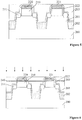
- FIG. 1 illustrates a cross-sectional view of the electrostatic discharge protection structure shown in fig. 1 along a dashed line 1-2.
- the electrostatic discharge protection structure includes a substrate 100, a fin portion 101, a first well region 121, a second well region 122, an isolation structure 102, a gate structure 110, a source region 112, and a drain region 111.
- the fin portion 101 is on the substrate 100.
- the first well region 121 is in the fin portion 101 and the substrate 100.
- the second well region 122 is in the fin portion 101 and the substrate 100, and is in contact with the first well region 121.
- the isolation structure 102 is on the substrate 100, and covers a part of sidewalls of the fin portion 101.
- the gate structure 110 spans the fin portion 101, and covers a part of the sidewalls and top surface of the fin portion 101.
- the source region 112 and the drain region 111 are in the fin portion 101, and on the two sides of the gate structure 110 respectively.
- the electrostatic discharge protection structure When the electrostatic discharge protection structure is in operation, a large amount of electrostatic current can flow into the drain region 111 to generate a large amount of heat. Since the drain region 111 is in contact with only the fin portion 101, and the contact area between the drain region 111 and the substrate is small, the heat generated by the electrostatic current is hardly released. Thus, a sharp rise of the temperature of the electrostatic discharge protection structure can be caused, which is liable to damage the fin portion 101, and thereby resulting in an unstable performance of the electrostatic discharge device.
- the present invention provides an improved method for fabricating an electrostatic discharge protection structure.
- the method can include the following steps. First, a base substrate including a first region and a second region can be provided.
- the second region of the substrate can include a substrate and a fin portion on the substrate. Further, a first doped layer can be formed on the base substrate in the first region. Then, a second doped layer can be formed on the surface of the fin portion and the surface of the based substrate in the second region.
- the second doped layer is formed not only on the surface of the fin portion in the second region, but also on the surface of the base substrate in the second region. As such, the contact area between the second doped layer and the base substrate can be enlarged, thereby increasing the current flow through the cross-sectional area of the channel. Therefore, the disclosed method can increase the heat dissipation performance of the formed electrostatic discharge protection structure, and can improve the performance of the formed electrostatic discharge protection structure.
- FIG. 11 a schematic flow diagram of an exemplary process for fabricating an electrostatic discharge protection structure is shown in accordance with some embodiments of the disclosed subject matter.
- FIGs. 3-10 illustrate schematic structural views of an exemplary electrostatic discharge protection structure at certain stages of the fabricating process shown in fig. 11.
- the drain of the electrostatic discharge structure under an effect of a large electrostatic current is easy to produce large amounts of heat. Therefore, the electrostatic discharge protection structure has a high requirement of the heat dissipation performance.
- the method for fabricating the electrostatic discharge protection structure according to the present invention is described in details by using the heat dissipation performance of the electrostatic discharge protection structure as an example.
- the method of the present invention is not limited to fabricate the electrostatic discharge protection structure, but can also be applied to the formation of other semiconductor devices such as diodes and transistors.
- a base substrate including a first region and a second region can be provided.
- the base substrate in the second region can include a substrate and multiple fin portions on the substrate
- the first region i in fig. 4 shows a cross-sectional view of the structure in fig. 3 along the dashed line 11-12
- the second region ii in fig. 4 shows a cross-sectional view of the structure in fig. 3 along the dashed line 21-22.
- a base substrate including the first region i and the second region ii can be provided.
- the second region ii of the base substrate includes a substrate 200 and multiple fin portions 201 on the substrate 200.
- the first region i can be used for forming a source region, and the second region ii can be used for forming a drain region. In some other embodiments, the first region can be used d to form a drain region, and the second region can be used to form a source region.
- the base substrate in the first region i can also include the substrate 200 and the multiple fin portions 201 on the substrate 200.
- the base substrate can include multiple fin portions 201 on the substrate 200 in the second region ii, as well as multiple fin portions 201 on the substrate 200 in the first region i.
- the base substrate can further include a gate region iii between the first region i and the second region ii.
- the gate region iii can be used for forming a gate structure.
- the base substrate can further include an isolation region iv between the gate region iii and the second region ii. In some other embodiments, the base substrate may not include the gate region and the isolation region.
- the process of forming the base substrate can include the following steps. First, an initial substrate can be provided. Furtherfurther, the initial substrate can be patterned to form the substrate 200 and initial fin portions on the substrate 200. Then, the initial fin portions on the isolation region iv can be removed to form the multiple fin portions 201.
- the substrate 200 can be a silicon substrate. In some other embodiments, the substrate 200 may also be a semiconductor substrate such as a germanium substrate, a silicon germanium substrate, or a silicon-on-insulator substrate.
- the material of the multiple fin portions 201 can be silicon. In some other embodiments, the material of the multiple fin portions 201 may also be germanium or silicon germanium.
- the initial fin portions on the isolation region iv can be removed by using a dry etching method or a wet etching method.
- the method can further include the following steps.
- a first well region (not shown in the figures) can be formed in the base substrate in the first region i and the gate region iii.
- a second well region (not shown in the figures) can be formed in the base substrate in the gate region iii, the isolation region iv and the second region ii. The second well region can be in contact with the first well region.
- the first well region has first dopant ions
- the second well region has second dopant ions.
- the type of the second dopant ions is opposite with the type of the first dopant ions.
- the type of the first dopant ions is n-type and the type of the second dopant ions is p-type.
- the type of the first dopant ions is p-type and the type of the second dopant ions is n-type.
- an isolation structure can be formed on the substrate in the first region and the second region.
- an isolation structure 202 can be formed on the substrate in the first region i and the second region ii.
- the isolation structure 202 can cover a portion of sidewalls of the multiple fin portions 201.
- a top surface of the isolation structure 202 can be lower than the top surface of the multiple fin portions 201.
- the isolation structure 202 can be used to achieve an isolation between the multiple fin portions 201 in the first region i for reducing the leakage current.
- the material of the isolation structure 202 can be silicon oxide. In some other embodiments, the material of the isolation structure 202 may also be silicon oxynitride.
- a process for forming the isolation structure 202 can include the following steps. First, an initial isolation structure can be formed to cover the sidewalls and the top surface of the multiple fin portions 201. Further, the initial isolation structure can be etched to form the isolation structure 202, such that the top surface of the isolation structure 202 is lower than the top surface of the multiple fin portions 201 top surface.
- the method of etching the initial isolation structure can include a dry etching process. In some other embodiments, the method of etching the initial isolation structure may also include a wet etching process.
- the isolation structure 202 can also cover the substrate 200 in the isolation region iv, as shown in fig. 3 .
- the isolation structure 202 on the substrate 200 in the isolation region iv can be used to increase the length of the channel that the current flows through, thereby the heat dissipation performance of the formed electrostatic discharge protection structure can be enhanced.
- the isolation structure 202 can also be located on the substrate 200 between the multiple fin portions 201 in the gate region iii.
- step 1105 the isolation structure in the second region to expose the surface of the substrate in the second region.
- the isolation structure 202 on the substrate 200 in the second region ii can be removed to expose the surface of the substrate 200 in the second region ii.
- the surface of the substrate 200 in the second region ii is exposed to enable the formation of a subsequently formed second doped layer on the surface of the substrate 200 in the second region ii.
- the contact area between the second doped layer and the base substrate can be increased, thereby increasing the cross-sectional area of the channel that the current flows through. Therefore, the heat dissipation performance of the formed electrostatic discharge protection structure can be enhanced.
- the process for removing the isolation structure 202 on the substrate 200 in the second region ii can include the following steps. First, a first photoresist film can be formed on the substrate 200 in the first region i. The first photoresist film can cover the sidewalls and top surface of the multiple fin portions 201 in the first region i. Further, the isolation structure 202 can be etched by using the first photoresist film as a mask. The isolation structure 202 on the substrate 200 in the second region ii can be removed. Finally, the first photoresist film can be removed.
- the method of removing the isolation structure 202 on the substrate 200 in the second region ii can include a wet etching process, a dry etching process, or a combination thereof.
- the isolation structure 202 on the substrate 200 in the second region ii can be removed, and the isolation structure 202 on the substrate 200 in the first region i can be retained.
- the isolation structure on the substrate in the first region may also be removed during the removal of the isolation structure on the substrate in the second region. As such, the substrate in the first region can be exposed. Therefore, in a subsequent epitaxial growth process, a first doped region can also be formed on the substrate in the first region, thereby further enhancing the heat dissipation performance of the formed electrostatic discharge protection structure.
- the substrate does not include the gate region and the isolation region, so that the fabricating method may not include the steps of forming the isolation structure and removing the isolation structure in the second region.
- the multiple fin portions in the second region can be etched to reduce a thickness of the multiple fin portions in the second region.
- the fabricating method can subsequently include etching the multiple fin portions 201 in the second region ii to reduce the thickness of the multiple fin portions 201 in the second region ii.
- a first sacrificial layer 203 can be formed in the first region i.
- the first sacrificial layer 203 can cover the sidewalls and top surface of the multiple fin portions 201 in the first region i.
- a second sacrificial layer 204 can be formed on the substrate 200 in the second region ii.
- the top surface of the second sacrificial layer 204 can be lower than the top surface of the multiple fin portions 201 in the second region ii.
- the base substrate can further include the gate region iii between the first region i and the second region ii, as shown in fig. 3 .
- the first sacrificial layer 203 can also cover the sidewalls and top surface of the multiple fin portions 201 in the gate region iii.
- the first sacrificial layer 203 and the second sacrificial layer 204 can be antireflective coatings.
- the antireflective coatings can be organic antireflective coatings, since a removal process of the organic anti-reflective coatings is relatively simple.
- the material of the first sacrificial layer and the second sacrificial layer may also be silicon oxide, silicon nitride, or silicon oxynitride.
- the process of forming the first sacrificial layer 203 and the second sacrificial layer 204 can include the following steps. Firstly, an initial sacrificial layer can be formed to cover the substrate in the first region i, the second region ii, and the gate region iii. Then, a second photoresist film can be formed on the initial sacrificial layer in the first region i and the gate region iii. Further, the initial sacrificial layer can be etched by using the second photoresist film as a mask, such that the top surface of the initial sacrificial layer in the second region ii is lower than the top surface of the multiple fin portions 201 in the second region ii. Finally, the second photoresist film can be removed.
- the method of etching the initial sacrificial layer by using the second photoresist film as a mask can include a dry etching process or a wet etching process.
- the first sacrificial layer may not cover the first region substrate, thereby exposing the multiple fin portions in the first region.
- the multiple fin portions 201 in the second region ii can be etched to reduce the height of the multiple fin portions 201 in the second region ii.
- the height of the multiple fin portions 201 in the second region ii can be reduced to decrease the aspect ratio of the gaps between adjacent fin portions 201 in the second region ii.
- the reactant can be sufficiently in contact with the substrate 200 in the second region ii to form the second doped layer on the substrate 200 in the second region ii.
- the multiple fin portions 201 in the second region ii can be etched using the first sacrificial layer 203 and the second sacrificial layer 204 as masks.
- a contact area between the subsequently formed second doped layer and the sidewalls of the multiple fin portions 201 may be too small to improve the heat dissipation performance of the formed electrostatic discharge protection structure.
- the height of the multiple fin portions 201 in the second region ii is too large, it is difficult to reduce the difficulty of contacting the reaction gas with the substrate 200 in the second region ii during the formation of the second doped layer. As such, it may not be easy to form the second doped layer on the substrate 200 in the second region ii.
- the height of the multiple fin portions 201 in the second region ii can be in a range from 150 angstroms to 800 angstroms.
- the depth-to-width ratio of the gaps between adjacent fin portions 201 in the second region ii can be in a range from 1 to 4.
- the method of etching the multiple fin portions 201 in the second region ii can include a dry etching process, a wet etching process, or a combination thereof.
- the first sacrificial layer may not cover the substrate in the first region, thereby exposing the multiple fin portions in the first region. Accordingly, during the etching process of the multiple fin portions in the second region, the multiple fin portions in the first region may also be etched to reduce the height of the multiple fin portions in the first region.
- the first sacrificial layer 203 and the second sacrificial layer 204 can be removed.
- the first sacrificial layer 203 and the second sacrificial layer 204 are organic antireflective coatings, and the first sacrificial layer 203 and the second sacrificial layer 204 can be removed by using washing water in a photolithography process.
- the first sacrificial layer and the second sacrificial layer are silicon nitride, silicon oxide, or silicon oxynitride, which may be removed by using a dry etching process, a wet etching process, or a combination thereof.
- the multiple fin portions in the second region can be etched to reduce the height of the multiple fin portions in the second region.
- a process for etching the multiple fin portions in the second region can include the following steps. Firstly, a sacrificial layer can be formed in the first region, and the sacrificial layer can cover the sidewalls and top surface of the multiple fin portions in the first region. Then, the multiple fin portions in the second region can be etched by using the sacrificial layer as a mask. Finally, the sacrificial layer can be removed.
- the sacrificial layer can be used as a mask to etch the multiple fin portions in the second region. Therefore, the process flow of the fabrication method can be simplified.
- the multiple fin portions in the second region may also be etched before forming the isolation structure.
- a first doped layer can be formed on the surface of the fin portion in the first region.
- a second doped layer can be formed on the surface of the fin portion in the second region.
- the first region i in fig. 9 shows a cross-sectional view of the structure in fig. 10 along the dashed line b-b
- the second region ii in fig. 9 shows a cross-sectional view of the structure in fig. 10 along the dashed line a-a.
- a first doped layer 211 can be formed on the surface of the multiple fin portions 201 in the first region i
- a second doped layer 212 can be formed on the surface of the multiple fin portions 201 in the second region ii.
- the first doped layer 211 can be sued as a source region of a transistor, and the second doped layer 212 can be used as a drain region of the transistor.
- the first doped layer 211 and the second doped layer 212 can have a same type, and are both n-type semiconductors. Thus, the first doped layer 211 and the second doped layer 212 can be formed in a single process.
- the dopant ions in the first doped layer 211 and the second doped layer 212 can be the same type, and are both n-type ions.
- the specific dopant ions may be phosphorus ions or arsenic ions.
- dopant ions in the first doped layer and the second doped layer may also be different types.
- the first doped layer and the second doped layer may be both p-type semiconductors.
- the types of the first doped layer and the second doped layer may be different, and the first doped layer and the second doped layer are formed in different processes.
- the first doped layer 211 and the second doped layer 212 can be formed by using an epitaxial growth process. During the epitaxial growth process, the first doped layer 211 and the second doped layer 212 can be in-situ doped to form the dopant ions in the first and second doped layers 211 and 212 respectively. In some other embodiments, the first doped layer and the second doped layer may also be formed by an ion implantation process.
- the second doped layer 212 may also be formed on the surface of the substrate 200 in the second region ii during the epitaxial growth process. As such, the contact area between the second doped layer 212 and the base substrate can be increased, thereby increasing the area of the base substrate that receives electrostatic charge, and resulting in an enhancing of the heat dissipation performance of the formed electrostatic discharge protection structure.
- the first doped layer 211 and the second doped layer 212 can be used to form n-type semiconductors.
- the dopant ions can be phosphorus ions or arsenic ions.
- the first doped layer and the second doped layer are both p-type semiconductors, and the dopant ions can be boron ions or boron fluoride ions.
- the type of the first dopant ions in the first well region 221 is opposite to the type of the dopant ions of the first doped layer 211 and the second doped layer 212. Therefore, the first dopant ions are p-type ions, such as boron ions.
- the type of the second dopant ions in the second well region 222 is the same as the type of the dopant ions of the first doped layer 211 and the second doped layer 212. Therefore, the second dopant ions are n-type ions, such as phosphorus ions or arsenic ions.
- the material of the first doped layer 211 and the second doped layer 212 can be silicon germanium or silicon. In some other embodiments, the first doped layer and the second doped layer may also be p-type semiconductors, and the materials of the first doped layer and the second doped layer may be carbon- silicon or silicon.
- a thickness of the first doped layer 211 can be in a range from 100 angstroms to 500 angstroms, for example 400 angstroms.
- a thickness of the second doped layer 212 can be in a range from 50 angstroms to 500 angstroms, for example, 350 angstroms.
- a gate structure crossing the fin portion can be formed in a gate region.
- the fabricating method can further include forming a gate structure 210 across the multiple fin portions 201 in the gate region iii.
- the gate structure 210 can cover a portion of the sidewalls and top surface of the multiple fin portions 201 in the gate region iii.
- a channel can be formed in the first well region 221 and the second well region 222 of the multiple fin portions 201 below the gate structure 210.
- the gate structure 210 can include a gate dielectric layer and a gate electrode on the gate dielectric layer.
- the gate electrode can be a polysilicon gate electrode. In some other embodiments, the gate electrode may also be a metal gate electrode.
- the material of the gate dielectric layer can be silicon oxide. In some other embodiments, the material of the gate dielectric layer may also be a high-k dielectric material that has a dielectric constant greater than 3.9.
- the second doped layer can be formed not only on the surface of the multiple fin portions in the second region, but also on the surface of the substrate in the second region. Therefore, the contact area between the second doped layer and the base substrate can be increased, thereby increasing the cross-sectional area of the channel that the current flows through. Accordingly, the disclosed method can enhance the heat dissipation performance of the formed electrostatic discharge protection structure, and can improve the performance of the formed electrostatic discharge protection structure.
- fig. 11 can be executed or performed in any order or sequence not limited to the order and sequence shown and described in the figure. Also, some of the above steps of the flow diagram of fig. 11 can be executed or performed substantially simultaneously where appropriate or in parallel to reduce latency and processing times. Furthermore, it should be noted that fig. 11 is provided as an example only. At least some of the steps shown in the figure may be performed in a different order than represented, performed concurrently, or altogether omitted.
- the present invention also provides an electrostatic discharge protection structure.
- the electrostatic discharge protection structure can include a base substrate comprising a substrate 200 and multiple fin portions 201 on the substrate 200.
- the base substrate can include a first region i and a second region ii.
- a first doping layer 211 can be on the surface of the multiple fin portions 201 in the first region i.
- a second doping layer 212 can be on the surface of the multiple fin portions 201 and the substrate 200 in the second region ii.
- the first region i is used for forming a source region, and the second region ii is used for forming a drain region. In some other embodiments, the first region is used for forming a drain region, and the second region is used for forming a source region.
- the base substrate includes multiple fin portions 201 on the substrate 200 in the second region ii, and multiple fin portions 201 on the substrate 200 in the first region i.
- the base substrate can further include a gate region iii between the first region i and the second region ii.
- the gate region iii is used for forming a gate structure.
- the base substrate can further include an isolation region iv between the gate region iii and the second region ii. In some other embodiments, the base substrate may not include the gate region and the isolation region.
- the disclosed electrostatic discharge protection structure can further include a first well region 221 in the multiple fin portions 201 and the substrate 200, as well as a second well region 222 in the multiple fin portions 201 and the substrate 200.
- the second well region 222 can be in contact with the first well region 221.
- the first well region 221 has first dopant ions.
- the type of the first dopant ions are opposite to the type of dopant ions in the first doping layer 211.
- the second well region 212 has second dopant ions.
- the type of the second dopant ions are opposite to the type of the first dopant ions.
- the first dopant ions are p-type ions, such as boron ions.
- the second dopant ions are n-type ions, such as phosphorus ions or arsenic ions.
- the first dopant ions may be n-type ions, and the second dopant ions may be p-type ions.
- the substrate 200 can be a silicon substrate.
- the substrate may be any other suitable semiconductor substrate, such as a germanium substrate, a silicon germanium substrate, or a silicon-on-insulator substrate.
- the material of the multiple fin portions 201 is silicon. In some other embodiments, the material of the multiple fin portions may be germanium or silicon germanium.
- the electrostatic discharge protection structure can further include an isolation structure 202 between the multiple fin portions 201 in the first region i.
- the top surface of the isolation structure 202 can be lower than the top surface of the multiple fin portions 201 in the first region i.
- the isolation structure 202 can also be located on the substrate 200 in the isolation region iv.
- the isolation structure 202 on the substrate 200 in the isolation region iv can increase the length of the channel that current flows through, thereby increasing the heat dissipation performance of the formed electrostatic discharge protection structure.
- the height of the multiple fin portions 201 in the second region ii is lower than the height of the multiple fin portions 201 in the first region i.
- the height of the multiple fin portions 201 in the second region ii is lowered than the height of the multiple fin portions 201 in the gate region iii.
- the height of the multiple fin portions in the first region may be equal to the height of the multiple fin portions in the second region.
- the height of the multiple fin portions in the second region and in the first region may be lower than the height of the multiple fin portions in the gate region.
- the contact arear between the second doped layer and the sidewalls of the multiple fin portions 201 may be too small to improve the heat dissipation performance of the formed electrostatic discharge protection structure. If the height of the multiple fin portions 201 in the second region ii is too large, it is difficult to form the second doped layer on the substrate 200 in the second region ii. Specifically, the height of the multiple fin portions 201 in the second region ii can be in a range from 150 angstroms to 800 angstroms.
- the depth-to-width ratio of the gaps between adjacent fin portions 201 in the second region ii is smaller than the depth-to-width ratio of the gaps between adjacent fin portions 201 in the gate region iii. Since the depth-to-width ratio of the gaps between the multiple fin portions 201 in the second region ii is small, the second doped layer 212 can adequately cover the surface of the substrate 200 in the first region i. Specifically, the depth-to-width ratio of the gaps between the adjacent fin portions 201 in the second region ii can be in a range from 1 to 4.
- the second doped layer 212 on the substrate 200 in the second region ii can increase the contact area between the second doped layer 212 and the base substrate, thereby increasing the area of the base substrate that receives electrostatic charge, and resulting in an enhancing of the heat dissipation performance of the formed electrostatic discharge protection structure.
- the first doped layer 211 can be used as a source region of a transistor, and the second doped layer 212 can be used as a drain region of the transistor.
- the first doped layer 211 and the second doped layer 212 can have a same type and are both n-type semiconductors. In some other embodiments, the first doped layer 211 and the second doped layer 212 may be both p-type semiconductors. In addition, the types of the first doped layer 211 and second doped layer 212 may be different.
- the first doped layer 211 and the second doped layer 212 contain same type of dopant ions.
- the first doped layer 211 and the second doped layer 212 can be both n-type semiconductors.
- the dopant ions can be phosphorus ions or arsenic ions.
- both the first doped layer 211 and the second doped layer 212 are p-type semiconductors, and the dopant ions are boron ions or bf 2 ions.
- the material of the first doped layer 211 and the second doped layer 212 can be silicon germanium or silicon. In some other embodiments, the first doped layer 211 and the second doped layer 212 may be p-type semiconductors, and the material of the first doped layer 211 and second doped layer 212 may be carbon-carbon or silicon.
- the thickness of the first doped layer 211 can be in a range from 100 angstroms to 500 angstroms, for example 400 angstroms.
- a thickness of the second doped layer 212 can be in a range from 50 angstroms to 500 angstroms, for example, 350 angstroms.
- the electrostatic discharge protection structure can further include a gate structure 210 located in the gate region iii.
- the gate structure 210 can cover a portion of the sidewalls and top surface of the multiple fin portions 201 in the gate region iii.
- the gate structure 201 can include a gate dielectric layer, and a gate electrode on the gate dielectric layer.
- the gate electrode is a polysilicon gate electrode. In some other embodiments, the gate electrode may be a metal gate electrode.
- the material of the gate dielectric layer can be silicon oxide. In some other embodiments, the material of the gate dielectric layer may be a high-k dielectric material that has a dielectric constant greater than 3.9.
- the second doped layer can be formed not only on the surface of the multiple fin portions in the second region, but also on the surface of the substrate in the second region. Therefore, the contact area between the second doped layer and the base substrate can be increased, thereby increasing the cross-sectional area of the channel that the current flows through. Accordingly, the disclosed method can enhance the heat dissipation performance of the formed electrostatic discharge protection structure, and can improve the performance of the formed electrostatic discharge protection structure.
- an electrostatic discharge protection structure and a fabricating method thereof are provided.
Abstract
Description
- This application claims the priority of Chinese patent application no.
201610666917.4, filed on august 12, 2016 - The present invention generally relates to the field of semiconductor fabricating technology and, more particularly, relates to an electrostatic discharge protection structure and a fabricating method thereof.
- With the rapid development of semiconductor manufacturing technology, semiconductor devices are developing towards a direction of higher component density and a higher degree of integration. Transistors as the most basic semiconductor devices are currently being widely used and, with the increasing of the semiconductor device component density and the integration degree, the transistor size is getting smaller and smaller.
- In a fin field effect transistor (fin fet), the channel is projected over the surface of the substrate to form a fin structure, and the gate covers the top and sidewalls of the fin structure. As such, the inversion layer formed on each side of the channel can control the turning-on and turning-off of the circuit on both sides, thereby greatly improving the circuit control and reducing the leakage current. In addition, the 3d architecture of a fin fet can improve the integration of the fin fet. However, the width of the fin structure of a fin fet may be relatively narrow, which can make the cooling of the fin fet to be a significant challenge. Therefore, a self-heat problem of the fin fet may be caused, which can damage the fin structure of the fin fet.
- Especially, in an electrostatic discharge circuit, a large electrostatic current generated by external circuitry can flow into the drain of the electrostatic discharge circuit, which may easily lead to a sharp increase of the temperature of the drain, causing an instable performance of the electrostatic discharge device. Therefore, the heat dissipation performance of the electrostatic discharge circuit has a significant impact on the electrostatic discharge device.
- Accordingly, the existing fin field-effect transistors have the disadvantages of poor heat dissipation and instable transistor performance.
- It is an object of the present invention to provide an electrostatic discharge protection structure and a fabricating method thereof which solve one or more problems set forth above and other problems, in particular by which a semiconductor device such as a fin field-effect transistors may achieve an improved heat dissipation and stable performance.
- The object is achieved by the features of the respective independent claims. Further embodiments are defined in the respective dependent claims.
- A first aspect of present invention provides an electrostatic discharge protection structure, comprising: A base substrate including a substrate and a fin portion on the substrate, wherein the substrate includes a first region and a second region; a first doped layer on a surface of the fin portion in the first region; and a second doped layer on a surface of the fin portion in the second region and on a surface of the substrate in the second region.
- Preferably, the base substrate further includes a gate region between the first region and the second region; the electrostatic discharge protection structure further comprises a gate structure on the base substrate in the gate region; and the first doped layer and the second doped layer are of a same type.
- Preferably, the electrostatic discharge protection structure further comprises an isolation structure on the base substrate between the second region and the gate region.
- Preferably, the first doped layer is in contact with the second doped layer.
- Preferably, the first doped layer and the second doped layer are of opposite types.
- Preferably, a height of the fin portion in the second region is less than a height of the fin portion in the first region.
- Preferably, a height of the fin portion in the second region is in a range from 150 angstroms to 800 angstroms.
- Preferably, the base substrate includes a plurality of fin portions on the substrate in the second region.
- Preferably, a depth-to-width ratio of gaps between adjacent fin portions in the second region is in a range from 1 to 4.
- Preferably, a thickness of the second doped layer is in a range from 50 angstroms to 500 angstroms.
- A second aspect of the present invention provides a method for fabricating an electrostatic discharge protection structure, comprising: Providing a base substrate including a first region and a second region, wherein the base substrate in the second region includes a substrate and a fin portion on the substrate; Forming a first doped layer on a surface of a fin portion in the first region; and Forming a second doped layer on a surface of the fin portion in the second region and on a surface of the substrate in the second region.
- Preferably, the base substrate further includes a gate region between the first region and the second region, further comprising: Before forming the first doped layer and the second doped layer, forming a gate structure on the base substrate in the gate region; wherein the first doped layer and the second doped layer are of a same type.
- Preferably, an isolation structure is formed on the base substrate between the second region and the gate region.
- Preferably, forming the second doped layer includes using an epitaxial growth process.
- Preferably, the method further comprises: Before forming the second doped layer, etching the fin portion in the second region to reduce a height of the fin portion in the second region.
- Preferably, after etching the fin portion in the second region, the height of the fin portion in the second region is in a range from 150 angstroms to 800 angstroms.
- Preferably, the base substrate includes a plurality of fin portions on the substrate in the second region.
- Preferably, a depth-to-width ratio of gaps between adjacent fin portions in the second region is in a range from 1 to 4.
- Preferably, the substrate and the fin portion on the substrate are further located in the first region of the base substrate, further comprising: Before forming the first doped layer and the second doped layer, forming an isolation structure on the substrate in the first region and the second region, wherein the isolation structure covers a portion of sidewalls of the fin portion, a top surface of the isolation structure is lower than a top surface of the fin portion, and removing the isolation structure in the second region to expose a surface of the substrate in the second region.
- Preferably, the method further comprises: After forming the isolation structure, and before removing the isolation structure in the second region, etching the fin portion in the second region.
- Preferably, the method further comprises: After removing the isolation structure in the second region, etching the fin portion in the second region.
- Preferably, etching the fin portion in the second region includes: Forming a first sacrificial layer in the first region, wherein the first sacrificial layer covers sidewalls and a top surface of the fin portion in the first region; forming a second sacrificial layer in the second region substrate, wherein a top surface of the second sacrificial layer is lower than a top surface of the in portion in the second region; etching the fin portion in the second region by using the first sacrificial layer and the second sacrificial layer as masks; and removing the first sacrificial layer and the second sacrificial layer.
- Preferably, the method of claim 16, further comprises: During the process of removing the isolation structure on the substrate in the second region, removing the isolation structure on the substrate in the first region.
- Other aspects of the disclosed subject matter can be understood by those skilled in the art in light of the description, the claims, and the drawings of the present invention.
- Various objectives, features, and advantages of the present invention can be more fully appreciated with reference to the detailed description of the present invention when considered in connection with the following drawings, in which like reference numerals identify like elements. It should be noted that the following drawings are merely examples for illustrative purposes according to various disclosed embodiments and are not intended to limit the scope of the present invention.
-
Figs. 1 and 2 illustrate schematic structural views of an electrostatic discharge protection structure; -
figs. 3-10 illustrate schematic structural views of an exemplary electrostatic discharge protection structure at certain stages of a fabricating process in accordance with some embodiments of the disclosed subject matter; and - Fig. 11 illustrates a schematic flow diagram of an exemplary method for fabricating an electrostatic discharge protection structure in accordance with some embodiments of the disclosed subject matter.
- Reference input now be made in detail to exemplary embodiments of the invention, which are illustrated in the accompanying drawings in order to fully understand and to be able to implement the present invention and to realize the technical effect. It should be understood that the following description has been made only by way of example, but not to limit the present invention. Various embodiments of the present invention and various features in the embodiments that are not conflicted with each other can be combined and rearranged in various ways. Without departing from the spirit and scope of the disclosed subject matter, modifications, equivalents, or improvements to the disclosed subject matter are understandable to those skilled in the art and are intended to be encompassed within the scope of the present invention.
- In accordance with various embodiments, the present invention provides an electrostatic discharge protection structure and a fabricating method thereof.
- There are certain issues with some existing methods for fabricating an electrostatic discharge protection structure. For example, the formed electrostatic discharge protection structure may have a poor heat dissipation performance. The reasons why the electrostatic discharge protection structure is difficult to dissipate heat can be analyzed in the following.
- Referring to
figs. 1 and 2 , schematic structural views of an electrostatic discharge protection structure are shown.Fig. 2 illustrate a cross-sectional view of the electrostatic discharge protection structure shown infig. 1 along a dashed line 1-2. - As illustrated, the electrostatic discharge protection structure includes a
substrate 100, afin portion 101, a first well region 121, a second well region 122, an isolation structure 102, a gate structure 110, asource region 112, and adrain region 111. - The
fin portion 101 is on thesubstrate 100. The first well region 121 is in thefin portion 101 and thesubstrate 100. The second well region 122 is in thefin portion 101 and thesubstrate 100, and is in contact with the first well region 121. The isolation structure 102 is on thesubstrate 100, and covers a part of sidewalls of thefin portion 101. The gate structure 110 spans thefin portion 101, and covers a part of the sidewalls and top surface of thefin portion 101. Thesource region 112 and thedrain region 111 are in thefin portion 101, and on the two sides of the gate structure 110 respectively. - When the electrostatic discharge protection structure is in operation, a large amount of electrostatic current can flow into the
drain region 111 to generate a large amount of heat. Since thedrain region 111 is in contact with only thefin portion 101, and the contact area between thedrain region 111 and the substrate is small, the heat generated by the electrostatic current is hardly released. Thus, a sharp rise of the temperature of the electrostatic discharge protection structure can be caused, which is liable to damage thefin portion 101, and thereby resulting in an unstable performance of the electrostatic discharge device. - In order to solve the above described technical problem, the present invention provides an improved method for fabricating an electrostatic discharge protection structure. The method can include the following steps. First, a base substrate including a first region and a second region can be provided. The second region of the substrate can include a substrate and a fin portion on the substrate. Further, a first doped layer can be formed on the base substrate in the first region. Then, a second doped layer can be formed on the surface of the fin portion and the surface of the based substrate in the second region.
- During the formation of the second doped layer, the second doped layer is formed not only on the surface of the fin portion in the second region, but also on the surface of the base substrate in the second region. As such, the contact area between the second doped layer and the base substrate can be enlarged, thereby increasing the current flow through the cross-sectional area of the channel. Therefore, the disclosed method can increase the heat dissipation performance of the formed electrostatic discharge protection structure, and can improve the performance of the formed electrostatic discharge protection structure.
- The foregoing purposes, features and advantages of the present invention will become more apparent from the following detailed description of various embodiments of the present invention when taken in conjunction with the accompanying drawings.
- Referring to fig. 11, a schematic flow diagram of an exemplary process for fabricating an electrostatic discharge protection structure is shown in accordance with some embodiments of the disclosed subject matter.
Figs. 3-10 illustrate schematic structural views of an exemplary electrostatic discharge protection structure at certain stages of the fabricating process shown in fig. 11. - It should be noted that, the drain of the electrostatic discharge structure under an effect of a large electrostatic current is easy to produce large amounts of heat. Therefore, the electrostatic discharge protection structure has a high requirement of the heat dissipation performance. In the following described embodiments, the method for fabricating the electrostatic discharge protection structure according to the present invention is described in details by using the heat dissipation performance of the electrostatic discharge protection structure as an example. However, the method of the present invention is not limited to fabricate the electrostatic discharge protection structure, but can also be applied to the formation of other semiconductor devices such as diodes and transistors.
- As shown in fig. 11, at step s1101, a base substrate including a first region and a second region can be provided. The base substrate in the second region can include a substrate and multiple fin portions on the substrate
- Referring to
figs. 3 and 4 , the first region i infig. 4 shows a cross-sectional view of the structure infig. 3 along the dashed line 11-12, and the second region ii infig. 4 shows a cross-sectional view of the structure infig. 3 along the dashed line 21-22. - As illustrated, a base substrate including the first region i and the second region ii can be provided. The second region ii of the base substrate includes a
substrate 200 andmultiple fin portions 201 on thesubstrate 200. - In some embodiments, the first region i can be used for forming a source region, and the second region ii can be used for forming a drain region. In some other embodiments, the first region can be used d to form a drain region, and the second region can be used to form a source region.
- In some embodiments, the base substrate in the first region i can also include the
substrate 200 and themultiple fin portions 201 on thesubstrate 200. - In some embodiments, the base substrate can include
multiple fin portions 201 on thesubstrate 200 in the second region ii, as well asmultiple fin portions 201 on thesubstrate 200 in the first region i. - In some embodiments, the base substrate can further include a gate region iii between the first region i and the second region ii. The gate region iii can be used for forming a gate structure. The base substrate can further include an isolation region iv between the gate region iii and the second region ii. In some other embodiments, the base substrate may not include the gate region and the isolation region.
- In some embodiments, the process of forming the base substrate can include the following steps. First, an initial substrate can be provided. Furtherfurther, the initial substrate can be patterned to form the
substrate 200 and initial fin portions on thesubstrate 200. Then, the initial fin portions on the isolation region iv can be removed to form themultiple fin portions 201. - In some embodiments, the
substrate 200 can be a silicon substrate. In some other embodiments, thesubstrate 200 may also be a semiconductor substrate such as a germanium substrate, a silicon germanium substrate, or a silicon-on-insulator substrate. - In some embodiments, the material of the
multiple fin portions 201 can be silicon. In some other embodiments, the material of themultiple fin portions 201 may also be germanium or silicon germanium. - In some embodiments, the initial fin portions on the isolation region iv can be removed by using a dry etching method or a wet etching method.
- In some embodiments, after forming the base substrate, the method can further include the following steps. A first well region (not shown in the figures) can be formed in the base substrate in the first region i and the gate region iii. A second well region (not shown in the figures) can be formed in the base substrate in the gate region iii, the isolation region iv and the second region ii. The second well region can be in contact with the first well region.
- In some embodiments, the first well region has first dopant ions, and the second well region has second dopant ions. The type of the second dopant ions is opposite with the type of the first dopant ions. For example, the type of the first dopant ions is n-type and the type of the second dopant ions is p-type. As another example, the type of the first dopant ions is p-type and the type of the second dopant ions is n-type.
- referring to
figs. 5 to 9 , schematic views of the electrostatic discharge protection structure in certain subsequent steps on the basis offig. 4 . - Returning to fig. 11, at step s1103, an isolation structure can be formed on the substrate in the first region and the second region.
- Referring to
fig. 5 , anisolation structure 202 can be formed on the substrate in the first region i and the second region ii. Theisolation structure 202 can cover a portion of sidewalls of themultiple fin portions 201. A top surface of theisolation structure 202 can be lower than the top surface of themultiple fin portions 201. - The
isolation structure 202 can be used to achieve an isolation between themultiple fin portions 201 in the first region i for reducing the leakage current. - In some embodiments, the material of the
isolation structure 202 can be silicon oxide. In some other embodiments, the material of theisolation structure 202 may also be silicon oxynitride. - In some embodiments, a process for forming the
isolation structure 202 can include the following steps. First, an initial isolation structure can be formed to cover the sidewalls and the top surface of themultiple fin portions 201. Further, the initial isolation structure can be etched to form theisolation structure 202, such that the top surface of theisolation structure 202 is lower than the top surface of themultiple fin portions 201 top surface. - In some embodiments, the method of etching the initial isolation structure can include a dry etching process. In some other embodiments, the method of etching the initial isolation structure may also include a wet etching process.
- It should be noted that, the
isolation structure 202 can also cover thesubstrate 200 in the isolation region iv, as shown infig. 3 . Theisolation structure 202 on thesubstrate 200 in the isolation region iv can be used to increase the length of the channel that the current flows through, thereby the heat dissipation performance of the formed electrostatic discharge protection structure can be enhanced. - The
isolation structure 202 can also be located on thesubstrate 200 between themultiple fin portions 201 in the gate region iii. - Returning to fig. 11, at step 1105, the isolation structure in the second region to expose the surface of the substrate in the second region.
- Referring to
fig. 6 , theisolation structure 202 on thesubstrate 200 in the second region ii can be removed to expose the surface of thesubstrate 200 in the second region ii. - The surface of the
substrate 200 in the second region ii is exposed to enable the formation of a subsequently formed second doped layer on the surface of thesubstrate 200 in the second region ii. As such, the contact area between the second doped layer and the base substrate can be increased, thereby increasing the cross-sectional area of the channel that the current flows through. Therefore, the heat dissipation performance of the formed electrostatic discharge protection structure can be enhanced. - In some embodiments, the process for removing the
isolation structure 202 on thesubstrate 200 in the second region ii can include the following steps. First, a first photoresist film can be formed on thesubstrate 200 in the first region i. The first photoresist film can cover the sidewalls and top surface of themultiple fin portions 201 in the first region i. Further, theisolation structure 202 can be etched by using the first photoresist film as a mask. Theisolation structure 202 on thesubstrate 200 in the second region ii can be removed. Finally, the first photoresist film can be removed. - In some embodiments, the method of removing the
isolation structure 202 on thesubstrate 200 in the second region ii can include a wet etching process, a dry etching process, or a combination thereof. - In some embodiments, the
isolation structure 202 on thesubstrate 200 in the second region ii can be removed, and theisolation structure 202 on thesubstrate 200 in the first region i can be retained. - In some other embodiments, the isolation structure on the substrate in the first region may also be removed during the removal of the isolation structure on the substrate in the second region. As such, the substrate in the first region can be exposed. Therefore, in a subsequent epitaxial growth process, a first doped region can also be formed on the substrate in the first region, thereby further enhancing the heat dissipation performance of the formed electrostatic discharge protection structure.
- It should be noted that, in some other embodiments, the substrate does not include the gate region and the isolation region, so that the fabricating method may not include the steps of forming the isolation structure and removing the isolation structure in the second region.
- Returning to fig. 11, at step 1107, the multiple fin portions in the second region can be etched to reduce a thickness of the multiple fin portions in the second region.
- Referring to
figs. 7 and 8 , in some embodiments, after theisolation structure 202 in the second region ii is removed, the fabricating method can subsequently include etching themultiple fin portions 201 in the second region ii to reduce the thickness of themultiple fin portions 201 in the second region ii. - As shown in
fig. 7 , a firstsacrificial layer 203 can be formed in the first region i. The firstsacrificial layer 203 can cover the sidewalls and top surface of themultiple fin portions 201 in the first region i. A second sacrificial layer 204 can be formed on thesubstrate 200 in the second region ii. The top surface of the second sacrificial layer 204 can be lower than the top surface of themultiple fin portions 201 in the second region ii. - In some embodiments, the base substrate can further include the gate region iii between the first region i and the second region ii, as shown in
fig. 3 . And the firstsacrificial layer 203 can also cover the sidewalls and top surface of themultiple fin portions 201 in the gate region iii. - In some embodiments, the first
sacrificial layer 203 and the second sacrificial layer 204 can be antireflective coatings. The antireflective coatings can be organic antireflective coatings, since a removal process of the organic anti-reflective coatings is relatively simple. In some other embodiments, the material of the first sacrificial layer and the second sacrificial layer may also be silicon oxide, silicon nitride, or silicon oxynitride. - In some embodiments, the process of forming the first
sacrificial layer 203 and the second sacrificial layer 204 can include the following steps. Firstly, an initial sacrificial layer can be formed to cover the substrate in the first region i, the second region ii, and the gate region iii. Then, a second photoresist film can be formed on the initial sacrificial layer in the first region i and the gate region iii. Further, the initial sacrificial layer can be etched by using the second photoresist film as a mask, such that the top surface of the initial sacrificial layer in the second region ii is lower than the top surface of themultiple fin portions 201 in the second region ii. Finally, the second photoresist film can be removed. - In some embodiments, the method of etching the initial sacrificial layer by using the second photoresist film as a mask can include a dry etching process or a wet etching process.
- In some other embodiments, if the substrate in the first region does not have an isolation structure, the first sacrificial layer may not cover the first region substrate, thereby exposing the multiple fin portions in the first region.
- Referring to
fig. 8 , themultiple fin portions 201 in the second region ii can be etched to reduce the height of themultiple fin portions 201 in the second region ii. - In some embodiments, the height of the
multiple fin portions 201 in the second region ii can be reduced to decrease the aspect ratio of the gaps betweenadjacent fin portions 201 in the second region ii. As such, during the formation of the second doped layer, the reactant can be sufficiently in contact with thesubstrate 200 in the second region ii to form the second doped layer on thesubstrate 200 in the second region ii. - In some embodiments, the
multiple fin portions 201 in the second region ii can be etched using the firstsacrificial layer 203 and the second sacrificial layer 204 as masks. - In some embodiments, after etching the
multiple fin portions 201 in the second region ii, when the height of themultiple fin portions 201 in the second region ii is too small, a contact area between the subsequently formed second doped layer and the sidewalls of themultiple fin portions 201 may be too small to improve the heat dissipation performance of the formed electrostatic discharge protection structure. When the height of themultiple fin portions 201 in the second region ii is too large, it is difficult to reduce the difficulty of contacting the reaction gas with thesubstrate 200 in the second region ii during the formation of the second doped layer. As such, it may not be easy to form the second doped layer on thesubstrate 200 in the second region ii. Specifically, after etching themultiple fin portions 201 in the second region ii, the height of themultiple fin portions 201 in the second region ii can be in a range from 150 angstroms to 800 angstroms. - In some embodiments, after etching the
multiple fin portions 201 in the second region ii, the depth-to-width ratio of the gaps betweenadjacent fin portions 201 in the second region ii can be in a range from 1 to 4. - In some embodiments, the method of etching the
multiple fin portions 201 in the second region ii can include a dry etching process, a wet etching process, or a combination thereof. - It should be noted that, in some other embodiments, the first sacrificial layer may not cover the substrate in the first region, thereby exposing the multiple fin portions in the first region. Accordingly, during the etching process of the multiple fin portions in the second region, the multiple fin portions in the first region may also be etched to reduce the height of the multiple fin portions in the first region.
- Referring to
fig. 8 , the firstsacrificial layer 203 and the second sacrificial layer 204 can be removed. - In some embodiments, the first
sacrificial layer 203 and the second sacrificial layer 204 are organic antireflective coatings, and the firstsacrificial layer 203 and the second sacrificial layer 204 can be removed by using washing water in a photolithography process. - In some other embodiments, the first sacrificial layer and the second sacrificial layer are silicon nitride, silicon oxide, or silicon oxynitride, which may be removed by using a dry etching process, a wet etching process, or a combination thereof.
- It should be noted that, in some embodiments, after forming the isolation structure, and before removing the isolation structure in the second region, the multiple fin portions in the second region can be etched to reduce the height of the multiple fin portions in the second region.
- Specifically, after forming the isolation structure, and before removing the isolation structure in the second region, a process for etching the multiple fin portions in the second region can include the following steps. Firstly, a sacrificial layer can be formed in the first region, and the sacrificial layer can cover the sidewalls and top surface of the multiple fin portions in the first region. Then, the multiple fin portions in the second region can be etched by using the sacrificial layer as a mask. Finally, the sacrificial layer can be removed.
- Thus, after forming the isolation structure, and before removing the isolation structure in the second region, during the process for etching the multiple fin portions in the second region, the sacrificial layer can be used as a mask to etch the multiple fin portions in the second region. Therefore, the process flow of the fabrication method can be simplified.
- In some other embodiments, the multiple fin portions in the second region may also be etched before forming the isolation structure.
- Returning to fig. 11, at step s1109, a first doped layer can be formed on the surface of the fin portion in the first region. And at step s1111, a second doped layer can be formed on the surface of the fin portion in the second region.
- Referring to
figs. 9 and 10, the first region i infig. 9 shows a cross-sectional view of the structure in fig. 10 along the dashed line b-b, and the second region ii infig. 9 shows a cross-sectional view of the structure in fig. 10 along the dashed line a-a. As illustrated, a first dopedlayer 211 can be formed on the surface of themultiple fin portions 201 in the first region i, and a second doped layer 212 can be formed on the surface of themultiple fin portions 201 in the second region ii. - In some embodiments, the first doped
layer 211 can be sued as a source region of a transistor, and the second doped layer 212 can be used as a drain region of the transistor. In some embodiments, the first dopedlayer 211 and the second doped layer 212 can have a same type, and are both n-type semiconductors. Thus, the first dopedlayer 211 and the second doped layer 212 can be formed in a single process. - In some embodiments, the dopant ions in the first doped
layer 211 and the second doped layer 212 can be the same type, and are both n-type ions. The specific dopant ions may be phosphorus ions or arsenic ions. In some other embodiments, dopant ions in the first doped layer and the second doped layer may also be different types. - In some other embodiments, the first doped layer and the second doped layer may be both p-type semiconductors. In addition, the types of the first doped layer and the second doped layer may be different, and the first doped layer and the second doped layer are formed in different processes.
- In some embodiments, the first doped
layer 211 and the second doped layer 212 can be formed by using an epitaxial growth process. During the epitaxial growth process, the first dopedlayer 211 and the second doped layer 212 can be in-situ doped to form the dopant ions in the first and seconddoped layers 211 and 212 respectively. In some other embodiments, the first doped layer and the second doped layer may also be formed by an ion implantation process. - It should be noted that, since there is no isolation structure on the
substrate 200 in the second region ii, the second doped layer 212 may also be formed on the surface of thesubstrate 200 in the second region ii during the epitaxial growth process. As such, the contact area between the second doped layer 212 and the base substrate can be increased, thereby increasing the area of the base substrate that receives electrostatic charge, and resulting in an enhancing of the heat dissipation performance of the formed electrostatic discharge protection structure. - In some embodiments, the first doped
layer 211 and the second doped layer 212 can be used to form n-type semiconductors. In the in-situ doping process of the first dopedlayer 211 and the second doped layer 212, the dopant ions can be phosphorus ions or arsenic ions. In some other embodiments, the first doped layer and the second doped layer are both p-type semiconductors, and the dopant ions can be boron ions or boron fluoride ions. - It should be noted that, in some embodiments, the type of the first dopant ions in the
first well region 221 is opposite to the type of the dopant ions of the first dopedlayer 211 and the second doped layer 212. Therefore, the first dopant ions are p-type ions, such as boron ions. The type of the second dopant ions in thesecond well region 222 is the same as the type of the dopant ions of the first dopedlayer 211 and the second doped layer 212. Therefore, the second dopant ions are n-type ions, such as phosphorus ions or arsenic ions. - In some embodiments, the material of the first doped
layer 211 and the second doped layer 212 can be silicon germanium or silicon. In some other embodiments, the first doped layer and the second doped layer may also be p-type semiconductors, and the materials of the first doped layer and the second doped layer may be carbon- silicon or silicon. - In some embodiments, a thickness of the first doped
layer 211 can be in a range from 100 angstroms to 500 angstroms, for example 400 angstroms. A thickness of the second doped layer 212 can be in a range from 50 angstroms to 500 angstroms, for example, 350 angstroms. - Returning to fig. 11, at step s1113, a gate structure crossing the fin portion can be formed in a gate region.
- Referring to fig. 10, in some embodiments, before forming the first doped
layer 211 and the second doped layer 212, the fabricating method can further include forming agate structure 210 across themultiple fin portions 201 in the gate region iii. Thegate structure 210 can cover a portion of the sidewalls and top surface of themultiple fin portions 201 in the gate region iii. - In some embodiments, a channel can be formed in the
first well region 221 and thesecond well region 222 of themultiple fin portions 201 below thegate structure 210. - In some embodiments, the
gate structure 210 can include a gate dielectric layer and a gate electrode on the gate dielectric layer. - In some embodiments, the gate electrode can be a polysilicon gate electrode. In some other embodiments, the gate electrode may also be a metal gate electrode.
- In some embodiments, the material of the gate dielectric layer can be silicon oxide. In some other embodiments, the material of the gate dielectric layer may also be a high-k dielectric material that has a dielectric constant greater than 3.9.
- Thus, in the disclosed method for fabricating the electrostatic discharge protection structure of the various embodiments described above, the second doped layer can be formed not only on the surface of the multiple fin portions in the second region, but also on the surface of the substrate in the second region. Therefore, the contact area between the second doped layer and the base substrate can be increased, thereby increasing the cross-sectional area of the channel that the current flows through. Accordingly, the disclosed method can enhance the heat dissipation performance of the formed electrostatic discharge protection structure, and can improve the performance of the formed electrostatic discharge protection structure.
- It should be noted that the above steps of the flow diagram of fig. 11 can be executed or performed in any order or sequence not limited to the order and sequence shown and described in the figure. Also, some of the above steps of the flow diagram of fig. 11 can be executed or performed substantially simultaneously where appropriate or in parallel to reduce latency and processing times. Furthermore, it should be noted that fig. 11 is provided as an example only. At least some of the steps shown in the figure may be performed in a different order than represented, performed concurrently, or altogether omitted.
- Still referring to
figs. 9 and 10, in accordance with some embodiments, the present invention also provides an electrostatic discharge protection structure. As shown, the electrostatic discharge protection structure can include a base substrate comprising asubstrate 200 andmultiple fin portions 201 on thesubstrate 200. The base substrate can include a first region i and a second region ii. Afirst doping layer 211 can be on the surface of themultiple fin portions 201 in the first region i. A second doping layer 212 can be on the surface of themultiple fin portions 201 and thesubstrate 200 in the second region ii. - In some embodiments, the first region i is used for forming a source region, and the second region ii is used for forming a drain region. In some other embodiments, the first region is used for forming a drain region, and the second region is used for forming a source region.
- In some embodiments, the base substrate includes
multiple fin portions 201 on thesubstrate 200 in the second region ii, andmultiple fin portions 201 on thesubstrate 200 in the first region i. - In some embodiments, the base substrate can further include a gate region iii between the first region i and the second region ii. The gate region iii is used for forming a gate structure. The base substrate can further include an isolation region iv between the gate region iii and the second region ii. In some other embodiments, the base substrate may not include the gate region and the isolation region.
- In some embodiments, the disclosed electrostatic discharge protection structure can further include a
first well region 221 in themultiple fin portions 201 and thesubstrate 200, as well as asecond well region 222 in themultiple fin portions 201 and thesubstrate 200. Thesecond well region 222 can be in contact with thefirst well region 221. - In some embodiments, the
first well region 221 has first dopant ions. The type of the first dopant ions are opposite to the type of dopant ions in thefirst doping layer 211. The second well region 212 has second dopant ions. The type of the second dopant ions are opposite to the type of the first dopant ions. - Specifically, in some embodiments, the first dopant ions are p-type ions, such as boron ions. The second dopant ions are n-type ions, such as phosphorus ions or arsenic ions. In some other embodiments, the first dopant ions may be n-type ions, and the second dopant ions may be p-type ions.
- In some embodiments, the
substrate 200 can be a silicon substrate. In some other embodiments, the substrate may be any other suitable semiconductor substrate, such as a germanium substrate, a silicon germanium substrate, or a silicon-on-insulator substrate. - In some embodiments, the material of the
multiple fin portions 201 is silicon. In some other embodiments, the material of the multiple fin portions may be germanium or silicon germanium. - In some embodiments, the electrostatic discharge protection structure can further include an
isolation structure 202 between themultiple fin portions 201 in the first region i. The top surface of theisolation structure 202 can be lower than the top surface of themultiple fin portions 201 in the first region i. - In some embodiments, the
isolation structure 202 can also be located on thesubstrate 200 in the isolation region iv. Theisolation structure 202 on thesubstrate 200 in the isolation region iv can increase the length of the channel that current flows through, thereby increasing the heat dissipation performance of the formed electrostatic discharge protection structure. - In some embodiments, the height of the
multiple fin portions 201 in the second region ii is lower than the height of themultiple fin portions 201 in the first region i. The height of themultiple fin portions 201 in the second region ii is lowered than the height of themultiple fin portions 201 in the gate region iii. - In some other embodiments, the height of the multiple fin portions in the first region may be equal to the height of the multiple fin portions in the second region. The height of the multiple fin portions in the second region and in the first region may be lower than the height of the multiple fin portions in the gate region.
- In some embodiments, if the height of the
multiple fin portions 201 in the second region ii is too small, the contact arear between the second doped layer and the sidewalls of themultiple fin portions 201 may be too small to improve the heat dissipation performance of the formed electrostatic discharge protection structure. If the height of themultiple fin portions 201 in the second region ii is too large, it is difficult to form the second doped layer on thesubstrate 200 in the second region ii. Specifically, the height of themultiple fin portions 201 in the second region ii can be in a range from 150 angstroms to 800 angstroms. - In some embodiments, the depth-to-width ratio of the gaps between
adjacent fin portions 201 in the second region ii is smaller than the depth-to-width ratio of the gaps betweenadjacent fin portions 201 in the gate region iii. Since the depth-to-width ratio of the gaps between themultiple fin portions 201 in the second region ii is small, the second doped layer 212 can adequately cover the surface of thesubstrate 200 in the first region i. Specifically, the depth-to-width ratio of the gaps between theadjacent fin portions 201 in the second region ii can be in a range from 1 to 4. - It should be noted that, the second doped layer 212 on the
substrate 200 in the second region ii can increase the contact area between the second doped layer 212 and the base substrate, thereby increasing the area of the base substrate that receives electrostatic charge, and resulting in an enhancing of the heat dissipation performance of the formed electrostatic discharge protection structure. - In some embodiments, the first doped
layer 211 can be used as a source region of a transistor, and the second doped layer 212 can be used as a drain region of the transistor. - In some embodiment, the first doped
layer 211 and the second doped layer 212 can have a same type and are both n-type semiconductors. In some other embodiments, the first dopedlayer 211 and the second doped layer 212 may be both p-type semiconductors. In addition, the types of the first dopedlayer 211 and second doped layer 212 may be different. - In some embodiments, the first doped
layer 211 and the second doped layer 212 contain same type of dopant ions. The firstdoped layer 211 and the second doped layer 212 can be both n-type semiconductors. The dopant ions can be phosphorus ions or arsenic ions. In some other embodiments, both the first dopedlayer 211 and the second doped layer 212 are p-type semiconductors, and the dopant ions are boron ions or bf2 ions. - In some embodiments, the material of the first doped
layer 211 and the second doped layer 212 can be silicon germanium or silicon. In some other embodiments, the first dopedlayer 211 and the second doped layer 212 may be p-type semiconductors, and the material of the first dopedlayer 211 and second doped layer 212 may be carbon-carbon or silicon. - In some embodiments, the thickness of the first doped
layer 211 can be in a range from 100 angstroms to 500 angstroms, for example 400 angstroms. A thickness of the second doped layer 212 can be in a range from 50 angstroms to 500 angstroms, for example, 350 angstroms. - In some embodiments, the electrostatic discharge protection structure can further include a
gate structure 210 located in the gate region iii. Thegate structure 210 can cover a portion of the sidewalls and top surface of themultiple fin portions 201 in the gate region iii. - In some embodiments, the
gate structure 201 can include a gate dielectric layer, and a gate electrode on the gate dielectric layer. - In some embodiment, the gate electrode is a polysilicon gate electrode. In some other embodiments, the gate electrode may be a metal gate electrode.
- In some embodiments, the material of the gate dielectric layer can be silicon oxide. In some other embodiments, the material of the gate dielectric layer may be a high-k dielectric material that has a dielectric constant greater than 3.9.
- Thus, in the disclosed electrostatic discharge protection structure of the various embodiments described above, the second doped layer can be formed not only on the surface of the multiple fin portions in the second region, but also on the surface of the substrate in the second region. Therefore, the contact area between the second doped layer and the base substrate can be increased, thereby increasing the cross-sectional area of the channel that the current flows through. Accordingly, the disclosed method can enhance the heat dissipation performance of the formed electrostatic discharge protection structure, and can improve the performance of the formed electrostatic discharge protection structure.
- The provision of the examples described herein (as well as clauses phrased as "such as," "e.g.," "including," and the like) should not be interpreted as limiting the claimed subject matter to the specific examples; rather, the examples are intended to illustrate only some of many possible aspects.
- Accordingly, an electrostatic discharge protection structure and a fabricating method thereof are provided.
- Although the disclosed subject matter has been described and illustrated in the foregoing illustrative embodiments, it is understood that the present invention has been made only by way of example, and that numerous changes in the details of embodiment of the disclosed subject matter can be made without departing from the spirit and scope of the disclosed subject matter, which is only limited by the claims which follow. Features of the disclosed embodiments can be combined and rearranged in various ways. Without departing from the spirit and scope of the disclosed subject matter, modifications, equivalents, or improvements to the disclosed subject matter are understandable to those skilled in the art and are intended to be encompassed within the scope of the present invention.
Claims (15)
- An electrostatic discharge protection structure, comprising:a base substrate including a substrate and a fin portion on the substrate, wherein the substrate includes a first region and a second region;a first doped layer on a surface of the fin portion in the first region; anda second doped layer on a surface of the fin portion in the second region and on a surface of the substrate in the second region.
- The electrostatic discharge protection structure of claim 1, wherein:the base substrate further includes a gate region between the first region and the second region;the electrostatic discharge protection structure further comprises a gate structure on the base substrate in the gate region; andthe first doped layer and the second doped layer are of a same type; andpreferably, the electrostatic discharge protection structure further comprises an isolation structure on the base substrate between the second region and the gate region.
- The electrostatic discharge protection structure of claim 1 or 2, wherein at least one of:the first doped layer is in contact with the second doped layer; and the first doped layer and the second doped layer are of opposite types;a height of the fin portion in the second region is less than a height of the fin portion in the first region, preferably: the height of the fin portion in the second region is in a range from 150 angstroms to 800 angstroms;the base substrate includes a plurality of fin portions on the substrate in the second region, and a depth-to-width ratio of gaps between adjacent fin portions in the second region is in a range from 1 to 4; anda thickness of the second doped layer is in a range from 50 angstroms to 500 angstroms.
- A method for fabricating an electrostatic discharge protection structure, comprising:providing a base substrate including a first region and a second region, wherein the base substrate in the second region includes a substrate and a fin portion on the substrate;forming a first doped layer on a surface of a fin portion in the first region; andforming a second doped layer on a surface of the fin portion in the second region and on a surface of the substrate in the second region.
- The method of claim 4, wherein the base substrate further includes a gate region between the first region and the second region, further comprising:before forming the first doped layer and the second doped layer, forming a gate structure on the base substrate in the gate region;wherein the first doped layer and the second doped layer are of a same type.
- The method of claim 5, wherein an isolation structure is formed on the base substrate between the second region and the gate region.
- The method of anyone of the claims 4-6, wherein:forming the second doped layer includes using an epitaxial growth process.
- The method of anyone of the claims 4-7, further comprising:before forming the second doped layer, etching the fin portion in the second region to reduce a height of the fin portion in the second region.
- The method of claim 8, wherein:after etching the fin portion in the second region, the height of the fin portion in the second region is in a range from 150 angstroms to 800 angstroms.
- The method of claim 8 or 9, wherein:the base substrate includes a plurality of fin portions on the substrate in the second region; anda depth-to-width ratio of gaps between adjacent fin portions in the second region is in a range from 1 to 4.
- The method to anyone of the claims 8-10, wherein the substrate and the fin portion on the substrate are further located in the first region of the base substrate, further comprising:before forming the first doped layer and the second doped layer, forming an isolation structure on the substrate in the first region and the second region, wherein the isolation structure covers a portion of sidewalls of the fin portion, a top surface of the isolation structure is lower than a top surface of the fin portion, andremoving the isolation structure in the second region to expose a surface of the substrate in the second region.
- The method of claim 11, further comprising:after forming the isolation structure, and before removing the isolation structure in the second region, etching the fin portion in the second region.
- The method of claim 11 or 12, further comprising:after removing the isolation structure in the second region, etching the fin portion in the second region.
- The method of claim 13, wherein etching the fin portion in the second region includes:forming a first sacrificial layer in the first region, wherein the first sacrificial layer covers sidewalls and a top surface of the fin portion in the first region;forming a second sacrificial layer in the second region substrate, wherein a top surface of the second sacrificial layer is lower than a top surface of the in portion in the second region;etching the fin portion in the second region by using the first sacrificial layer and the second sacrificial layer as masks; andremoving the first sacrificial layer and the second sacrificial layer.
- The method of anyone of the claims 11-14, further comprising:during the process of removing the isolation structure on the substrate in the second region, removing the isolation structure on the substrate in the first region.
Applications Claiming Priority (1)
| Application Number | Priority Date | Filing Date | Title |
|---|---|---|---|
| CN201610666917.4A CN107731808B (en) | 2016-08-12 | 2016-08-12 | Electrostatic discharge protection structure and forming method thereof |
Publications (1)
| Publication Number | Publication Date |
|---|---|
| EP3285298A1 true EP3285298A1 (en) | 2018-02-21 |
Family
ID=59631594
Family Applications (1)
| Application Number | Title | Priority Date | Filing Date |
|---|---|---|---|
| EP17185877.2A Withdrawn EP3285298A1 (en) | 2016-08-12 | 2017-08-11 | Electrostatic discharge protection structure and fabricating method thereof |
Country Status (3)
| Country | Link |
|---|---|
| US (2) | US10354993B2 (en) |
| EP (1) | EP3285298A1 (en) |
| CN (1) | CN107731808B (en) |
Families Citing this family (3)
| Publication number | Priority date | Publication date | Assignee | Title |
|---|---|---|---|---|
| CN107731808B (en) * | 2016-08-12 | 2020-02-07 | 中芯国际集成电路制造(上海)有限公司 | Electrostatic discharge protection structure and forming method thereof |
| CN107799421B (en) * | 2016-09-05 | 2021-04-02 | 中芯国际集成电路制造(上海)有限公司 | Method for forming semiconductor device |
| CN113257921B (en) * | 2017-07-03 | 2023-06-13 | 中芯国际集成电路制造(上海)有限公司 | Semiconductor structure |
Citations (5)
| Publication number | Priority date | Publication date | Assignee | Title |
|---|---|---|---|---|
| DE102013101705A1 (en) * | 2012-11-15 | 2014-05-15 | Taiwan Semiconductor Manufacturing Co., Ltd. | ESD devices with semiconductor fins |
| EP2889906A1 (en) * | 2013-12-30 | 2015-07-01 | IMEC vzw | Improvements in or relating to electrostatic discharge protection |
| US20150311342A1 (en) * | 2014-04-23 | 2015-10-29 | Taiwan Semiconductor Manufacturing Company Ltd. | Finfet with esd protection |
| US20160093730A1 (en) * | 2014-09-26 | 2016-03-31 | Semiconductor Manufacturing International (Shanghai) Corporation | Finfet ldmos device and manufacturing methods |
| US20160181358A1 (en) * | 2014-12-22 | 2016-06-23 | Broadcom Corporation | Super junction ldmos finfet devices |
Family Cites Families (6)
| Publication number | Priority date | Publication date | Assignee | Title |
|---|---|---|---|---|
| US7700449B2 (en) * | 2008-06-20 | 2010-04-20 | Taiwan Semiconductor Manufacturing Company, Ltd. | Forming ESD diodes and BJTs using FinFET compatible processes |
| US8551841B2 (en) * | 2012-01-06 | 2013-10-08 | Taiwan Semiconductor Manufacturing Company, Ltd. | IO ESD device and methods for forming the same |
| US9093566B2 (en) * | 2012-12-31 | 2015-07-28 | Taiwan Semiconductor Manufacturing Company, Ltd. | High efficiency FinFET diode |
| KR102049774B1 (en) * | 2013-01-24 | 2019-11-28 | 삼성전자 주식회사 | Semiconductor device and fabricated method thereof |
| US9916978B2 (en) * | 2016-06-02 | 2018-03-13 | United Microelectronics Corporation | Method for fabricating a Fin field effect transistor (FinFET) |
| CN107731808B (en) * | 2016-08-12 | 2020-02-07 | 中芯国际集成电路制造(上海)有限公司 | Electrostatic discharge protection structure and forming method thereof |
-
2016
- 2016-08-12 CN CN201610666917.4A patent/CN107731808B/en active Active
-
2017
- 2017-08-11 EP EP17185877.2A patent/EP3285298A1/en not_active Withdrawn
- 2017-10-05 US US15/725,854 patent/US10354993B2/en active Active
-
2019
- 2019-05-31 US US16/427,711 patent/US10714469B2/en active Active
Patent Citations (5)
| Publication number | Priority date | Publication date | Assignee | Title |
|---|---|---|---|---|
| DE102013101705A1 (en) * | 2012-11-15 | 2014-05-15 | Taiwan Semiconductor Manufacturing Co., Ltd. | ESD devices with semiconductor fins |
| EP2889906A1 (en) * | 2013-12-30 | 2015-07-01 | IMEC vzw | Improvements in or relating to electrostatic discharge protection |
| US20150311342A1 (en) * | 2014-04-23 | 2015-10-29 | Taiwan Semiconductor Manufacturing Company Ltd. | Finfet with esd protection |
| US20160093730A1 (en) * | 2014-09-26 | 2016-03-31 | Semiconductor Manufacturing International (Shanghai) Corporation | Finfet ldmos device and manufacturing methods |
| US20160181358A1 (en) * | 2014-12-22 | 2016-06-23 | Broadcom Corporation | Super junction ldmos finfet devices |
Also Published As
| Publication number | Publication date |
|---|---|
| CN107731808A (en) | 2018-02-23 |
| US10354993B2 (en) | 2019-07-16 |
| US20180158813A1 (en) | 2018-06-07 |
| US20190287958A1 (en) | 2019-09-19 |
| CN107731808B (en) | 2020-02-07 |
| US10714469B2 (en) | 2020-07-14 |
Similar Documents
| Publication | Publication Date | Title |
|---|---|---|
| US8946829B2 (en) | Selective fin-shaping process using plasma doping and etching for 3-dimensional transistor applications | |
| US8936986B2 (en) | Methods of forming finfet devices with a shared gate structure | |
| US9847419B2 (en) | Semiconductor device and fabrication method for forming the same | |
| US20170323888A1 (en) | Finfet and fabrication method thereof | |
| US9660054B2 (en) | Tunneling field effect transistor (TFET) with ultra shallow pockets formed by asymmetric ion implantation and method of making same | |
| US9640660B2 (en) | Asymmetrical FinFET structure and method of manufacturing same | |
| US10714469B2 (en) | Electrostatic discharge protection structure | |
| CN105097533A (en) | Forming method of semiconductor structure | |
| CN105551958B (en) | The forming method of transistor | |
| CN107731918B (en) | Semiconductor structure and manufacturing method thereof | |
| US20190393096A1 (en) | Semiconductor device and fabrication method thereof | |
| US10686078B2 (en) | Semiconductor structure and fabrication method thereof | |
| US11742414B2 (en) | Semiconductor device with fins | |
| CN107045981A (en) | The forming method of semiconductor structure | |
| CN109003899B (en) | Semiconductor structure, forming method thereof and forming method of fin field effect transistor | |
| US11682725B2 (en) | Semiconductor device with isolation layer | |
| CN107579108B (en) | Method for forming semiconductor structure | |
| US10748817B2 (en) | Semiconductor device and fabrication method thereof | |
| CN109003976B (en) | Semiconductor structure and forming method thereof | |
| CN108155100B (en) | Method for forming semiconductor device | |
| CN113838934A (en) | Semiconductor structure and forming method thereof | |
| US10978577B2 (en) | Semiconductor devices and fabrication methods thereof | |
| US10651092B2 (en) | Semiconductor device and fabrication method thereof | |
| CN109148297B (en) | Semiconductor device and method of forming the same | |
| CN115565877A (en) | Semiconductor structure and forming method thereof |
Legal Events
| Date | Code | Title | Description |
|---|---|---|---|
| PUAI | Public reference made under article 153(3) epc to a published international application that has entered the european phase |
Free format text: ORIGINAL CODE: 0009012 |
|
| AK | Designated contracting states |
Kind code of ref document: A1 Designated state(s): AL AT BE BG CH CY CZ DE DK EE ES FI FR GB GR HR HU IE IS IT LI LT LU LV MC MK MT NL NO PL PT RO RS SE SI SK SM TR |
|
| AX | Request for extension of the european patent |
Extension state: BA ME |
|
| 17P | Request for examination filed |
Effective date: 20180820 |
|
| RBV | Designated contracting states (corrected) |
Designated state(s): AL AT BE BG CH CY CZ DE DK EE ES FI FR GB GR HR HU IE IS IT LI LT LU LV MC MK MT NL NO PL PT RO RS SE SI SK SM TR |
|
| RAP1 | Party data changed (applicant data changed or rights of an application transferred) |
Owner name: SEMICONDUCTOR MANUFACTURING INTERNATIONAL (SHANGHA Owner name: SEMICONDUCTOR MANUFACTURING INTERNATIONAL (BEIJING |
|
| 17Q | First examination report despatched |
Effective date: 20191018 |
|
| STAA | Information on the status of an ep patent application or granted ep patent |
Free format text: STATUS: THE APPLICATION IS DEEMED TO BE WITHDRAWN |
|
| 18D | Application deemed to be withdrawn |
Effective date: 20200229 |