EP3285086A1 - Ultrasonic sensor and method for controlling same - Google Patents
Ultrasonic sensor and method for controlling same Download PDFInfo
- Publication number
- EP3285086A1 EP3285086A1 EP16779795.0A EP16779795A EP3285086A1 EP 3285086 A1 EP3285086 A1 EP 3285086A1 EP 16779795 A EP16779795 A EP 16779795A EP 3285086 A1 EP3285086 A1 EP 3285086A1
- Authority
- EP
- European Patent Office
- Prior art keywords
- ultrasonic sensor
- electrode
- reception
- transmission
- region
- Prior art date
- Legal status (The legal status is an assumption and is not a legal conclusion. Google has not performed a legal analysis and makes no representation as to the accuracy of the status listed.)
- Granted
Links
Images








Classifications
-
- G—PHYSICS
- G01—MEASURING; TESTING
- G01S—RADIO DIRECTION-FINDING; RADIO NAVIGATION; DETERMINING DISTANCE OR VELOCITY BY USE OF RADIO WAVES; LOCATING OR PRESENCE-DETECTING BY USE OF THE REFLECTION OR RERADIATION OF RADIO WAVES; ANALOGOUS ARRANGEMENTS USING OTHER WAVES
- G01S7/00—Details of systems according to groups G01S13/00, G01S15/00, G01S17/00
- G01S7/52—Details of systems according to groups G01S13/00, G01S15/00, G01S17/00 of systems according to group G01S15/00
- G01S7/521—Constructional features
-
- B—PERFORMING OPERATIONS; TRANSPORTING
- B06—GENERATING OR TRANSMITTING MECHANICAL VIBRATIONS IN GENERAL
- B06B—METHODS OR APPARATUS FOR GENERATING OR TRANSMITTING MECHANICAL VIBRATIONS OF INFRASONIC, SONIC, OR ULTRASONIC FREQUENCY, e.g. FOR PERFORMING MECHANICAL WORK IN GENERAL
- B06B1/00—Methods or apparatus for generating mechanical vibrations of infrasonic, sonic, or ultrasonic frequency
- B06B1/02—Methods or apparatus for generating mechanical vibrations of infrasonic, sonic, or ultrasonic frequency making use of electrical energy
- B06B1/0207—Driving circuits
- B06B1/0215—Driving circuits for generating pulses, e.g. bursts of oscillations, envelopes
-
- B—PERFORMING OPERATIONS; TRANSPORTING
- B06—GENERATING OR TRANSMITTING MECHANICAL VIBRATIONS IN GENERAL
- B06B—METHODS OR APPARATUS FOR GENERATING OR TRANSMITTING MECHANICAL VIBRATIONS OF INFRASONIC, SONIC, OR ULTRASONIC FREQUENCY, e.g. FOR PERFORMING MECHANICAL WORK IN GENERAL
- B06B1/00—Methods or apparatus for generating mechanical vibrations of infrasonic, sonic, or ultrasonic frequency
- B06B1/02—Methods or apparatus for generating mechanical vibrations of infrasonic, sonic, or ultrasonic frequency making use of electrical energy
- B06B1/06—Methods or apparatus for generating mechanical vibrations of infrasonic, sonic, or ultrasonic frequency making use of electrical energy operating with piezoelectric effect or with electrostriction
-
- B—PERFORMING OPERATIONS; TRANSPORTING
- B06—GENERATING OR TRANSMITTING MECHANICAL VIBRATIONS IN GENERAL
- B06B—METHODS OR APPARATUS FOR GENERATING OR TRANSMITTING MECHANICAL VIBRATIONS OF INFRASONIC, SONIC, OR ULTRASONIC FREQUENCY, e.g. FOR PERFORMING MECHANICAL WORK IN GENERAL
- B06B1/00—Methods or apparatus for generating mechanical vibrations of infrasonic, sonic, or ultrasonic frequency
- B06B1/02—Methods or apparatus for generating mechanical vibrations of infrasonic, sonic, or ultrasonic frequency making use of electrical energy
- B06B1/06—Methods or apparatus for generating mechanical vibrations of infrasonic, sonic, or ultrasonic frequency making use of electrical energy operating with piezoelectric effect or with electrostriction
- B06B1/0644—Methods or apparatus for generating mechanical vibrations of infrasonic, sonic, or ultrasonic frequency making use of electrical energy operating with piezoelectric effect or with electrostriction using a single piezoelectric element
- B06B1/0648—Methods or apparatus for generating mechanical vibrations of infrasonic, sonic, or ultrasonic frequency making use of electrical energy operating with piezoelectric effect or with electrostriction using a single piezoelectric element of rectangular shape
-
- G—PHYSICS
- G01—MEASURING; TESTING
- G01H—MEASUREMENT OF MECHANICAL VIBRATIONS OR ULTRASONIC, SONIC OR INFRASONIC WAVES
- G01H11/00—Measuring mechanical vibrations or ultrasonic, sonic or infrasonic waves by detecting changes in electric or magnetic properties
- G01H11/06—Measuring mechanical vibrations or ultrasonic, sonic or infrasonic waves by detecting changes in electric or magnetic properties by electric means
- G01H11/08—Measuring mechanical vibrations or ultrasonic, sonic or infrasonic waves by detecting changes in electric or magnetic properties by electric means using piezoelectric devices
-
- G—PHYSICS
- G01—MEASURING; TESTING
- G01S—RADIO DIRECTION-FINDING; RADIO NAVIGATION; DETERMINING DISTANCE OR VELOCITY BY USE OF RADIO WAVES; LOCATING OR PRESENCE-DETECTING BY USE OF THE REFLECTION OR RERADIATION OF RADIO WAVES; ANALOGOUS ARRANGEMENTS USING OTHER WAVES
- G01S15/00—Systems using the reflection or reradiation of acoustic waves, e.g. sonar systems
- G01S15/02—Systems using the reflection or reradiation of acoustic waves, e.g. sonar systems using reflection of acoustic waves
- G01S15/06—Systems determining the position data of a target
- G01S15/08—Systems for measuring distance only
- G01S15/10—Systems for measuring distance only using transmission of interrupted, pulse-modulated waves
-
- G—PHYSICS
- G01—MEASURING; TESTING
- G01S—RADIO DIRECTION-FINDING; RADIO NAVIGATION; DETERMINING DISTANCE OR VELOCITY BY USE OF RADIO WAVES; LOCATING OR PRESENCE-DETECTING BY USE OF THE REFLECTION OR RERADIATION OF RADIO WAVES; ANALOGOUS ARRANGEMENTS USING OTHER WAVES
- G01S7/00—Details of systems according to groups G01S13/00, G01S15/00, G01S17/00
- G01S7/52—Details of systems according to groups G01S13/00, G01S15/00, G01S17/00 of systems according to group G01S15/00
- G01S7/523—Details of pulse systems
- G01S7/524—Transmitters
-
- G—PHYSICS
- G01—MEASURING; TESTING
- G01S—RADIO DIRECTION-FINDING; RADIO NAVIGATION; DETERMINING DISTANCE OR VELOCITY BY USE OF RADIO WAVES; LOCATING OR PRESENCE-DETECTING BY USE OF THE REFLECTION OR RERADIATION OF RADIO WAVES; ANALOGOUS ARRANGEMENTS USING OTHER WAVES
- G01S7/00—Details of systems according to groups G01S13/00, G01S15/00, G01S17/00
- G01S7/52—Details of systems according to groups G01S13/00, G01S15/00, G01S17/00 of systems according to group G01S15/00
- G01S7/523—Details of pulse systems
- G01S7/526—Receivers
-
- H—ELECTRICITY
- H04—ELECTRIC COMMUNICATION TECHNIQUE
- H04R—LOUDSPEAKERS, MICROPHONES, GRAMOPHONE PICK-UPS OR LIKE ACOUSTIC ELECTROMECHANICAL TRANSDUCERS; ELECTRIC HEARING AIDS; PUBLIC ADDRESS SYSTEMS
- H04R17/00—Piezoelectric transducers; Electrostrictive transducers
-
- H—ELECTRICITY
- H04—ELECTRIC COMMUNICATION TECHNIQUE
- H04R—LOUDSPEAKERS, MICROPHONES, GRAMOPHONE PICK-UPS OR LIKE ACOUSTIC ELECTROMECHANICAL TRANSDUCERS; ELECTRIC HEARING AIDS; PUBLIC ADDRESS SYSTEMS
- H04R3/00—Circuits for transducers
Definitions
- the present disclosure relates to an ultrasonic sensor that includes a piezoelectric element, and more specifically, relates to control of an ultrasonic sensor.
- Ultrasonic sensors that include piezoelectric elements are known.
- An ultrasonic sensor causes a piezoelectric element to vibrate by applying an alternating-current voltage to a piezoelectric element, and as a result transmits an ultrasonic wave.
- the ultrasonic sensor detects an object on the basis of reception of an ultrasonic wave reflected by the object.
- Patent Document 1 discloses an ultrasonic wave output device that is capable of suppressing a reverberant vibration.
- Patent Document 1 Japanese Unexamined Patent Application Publication No. 2009-4916
- the ultrasonic wave output device disclosed in Patent Document 1 is formed of a detection part that detects a reverberant vibration and a transmission/reception part that transmits/receives ultrasonic waves.
- the ultrasonic wave output device generates a signal for suppressing a reverberant vibration in accordance with a reverberant vibration detected by the detection part. After that, the ultrasonic wave output device suppresses the reverberant vibration by feeding the generated signal back to the transmission/reception part. Since the detection part for detecting a reverberant vibration is additionally provided in the ultrasonic wave output device, a circuit configuration for feeding the signal for suppressing the reverberant vibration back to the transmission/reception part is required. Consequently, the circuit configuration becomes more complex.
- the present disclosure was made in order to solve the above-described problem and an object of a certain aspect thereof is to provide an ultrasonic sensor that can suppress a reverberant vibration with a simpler circuit configuration than has been possible to date.
- An object of another aspect thereof is to provide a control method for an ultrasonic sensor that can suppress a reverberant vibration with a simpler circuit configuration than has previously been possible.
- an ultrasonic sensor that includes a piezoelectric element.
- the piezoelectric element includes: a flat-plate-shaped piezoelectric body that includes a transmission region that is for transmitting an ultrasonic wave in response to having an alternating-current voltage applied thereto and a reception region that is for receiving a reflected wave of the ultrasonic wave; a common electrode that is provided in the transmission region and the reception region; a transmission electrode that is arranged so as to face the common electrode with the transmission region interposed therebetween and that is provided in the transmission region; and a reception electrode that is arranged so as to face the common electrode with the reception region interposed therebetween and that is provided in the reception region.
- the ultrasonic sensor further includes a semiconductor element that is electrically connected to the transmission electrode and the reception electrode and switches an electrical path extending between the transmission electrode and the reception electrode between a conductive state and a non-conductive state.
- the semiconductor element preferably puts the path into the conductive state after application of the alternating-current voltage is stopped, and as a result a reverberation signal, which is output from the reception region in accordance with a reverberant vibration of the ultrasonic wave, is fed back to the transmission electrode.
- the semiconductor element preferably switches the path from the conductive state to the non-conductive state after the reverberation signal has been fed back to the transmission electrode.
- the ultrasonic sensor preferably further includes an amplifier that is connected in series with the semiconductor element along the path.
- the amplifier amplifies the reverberation signal and outputs the amplified reverberation signal to the transmission electrode.
- the ultrasonic sensor preferably further includes an I/V conversion circuit that convert a current into a voltage.
- the I/V conversion circuit is provided along the path.
- the I/V conversion circuit preferably filters a signal of a frequency band that causes the ultrasonic sensor to undergo abnormal oscillation.
- the I/V conversion circuit preferably includes an operational amplifier and a capacitor.
- An inverting input terminal of the operational amplifier is electrically connected to the reception electrode.
- An output terminal of the operational amplifier is electrically connected to the amplifier.
- the capacitor is electrically connected to the inverting input terminal and the output terminal.
- the ultrasonic sensor preferably further includes a reception circuit that is electrically connected to the I/V conversion circuit.
- the ultrasonic sensor preferably has a plurality of operation modes having different detection distances from each other. Control conditions of the piezoelectric element are associated in advance with the plurality of operation modes in accordance with the detection distances. The ultrasonic sensor sequentially switches between the plurality of operation modes and controls the piezoelectric element using the control conditions corresponding to a current operation mode.
- the ultrasonic sensor preferably has a first operation mode and a second operation mode that has a longer detection distance than the first operation mode.
- the ultrasonic sensor executes processing to feed the reverberation signal back to the transmission electrode in the first operation mode and does not execute processing to feed the reverberation signal back to the transmission electrode in the second operation mode.
- the ultrasonic sensor preferably further includes a step up transformer that is provided along the path.
- the ultrasonic sensor includes a piezoelectric element.
- the piezoelectric element includes: a flat-plate-shaped piezoelectric body that includes a transmission region that is for transmitting an ultrasonic wave in response to having an alternating-current voltage applied thereto and a reception region that is for receiving a reflected wave of the ultrasonic wave; a common electrode that is provided in the transmission region and the reception region; a transmission electrode that is arranged so as to face the common electrode with the transmission region interposed therebetween and that is provided in the transmission region; and a reception electrode that is arranged so as to face the common electrode with the reception region interposed therebetween and that is provided in the reception region.
- the ultrasonic sensor further includes a semiconductor element that is electrically connected to the transmission electrode and the reception electrode and switches an electrical path extending between the transmission electrode and the reception electrode between a conductive state and a non-conductive state.
- the control method includes: a step of putting the path into the non-conductive state; a step of applying an alternating-current voltage to the transmission region after the path has been put into the non-conductive state; and a step of feeding a reverberation signal, which is output from the reception region in accordance with a reverberant vibration of the ultrasonic wave, back to the transmission electrode by putting the path into the conductive state after stopping application of the alternating-current voltage.
- a reverberant vibration can be suppressed with a simpler circuit configuration than was previously possible.
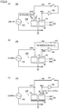
- Fig. 1 illustrates an example of the circuit configuration of the ultrasonic sensor 100.
- the ultrasonic sensor 100 is installed in a vehicle or a smartphone, for example.
- the ultrasonic sensor 100 measures the distance from itself to an object in accordance with the time taken from transmitting an ultrasonic wave until receiving a reflected wave.
- the ultrasonic sensor 100 detects the existence of an object on the basis of reception of a reflected wave.
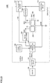
- the ultrasonic sensor 100 includes a control circuit 101, a memory 102, a signal generating circuit 104, a power source 105, a semiconductor element 107, an amplifier 108, a reception circuit 110 and a piezoelectric element 200.
- the control circuit 101 is a microcomputer, for example.
- the semiconductor element 107 is a transistor, for example.
- the control circuit 101 switches an electrical path 109, which extends between a transmission electrode 10 and a reception electrode 20, between a conductive state and a non-conductive state by driving the semiconductor element 107.
- the control circuit 101 reads out data stored in the memory 102 and outputs an appropriate control signal for driving the ultrasonic sensor 100 to the signal generating circuit 104.
- the power source 105 outputs a direct-current voltage of 12 V, for example, to the signal generating circuit 104.
- the signal generating circuit 104 generates an alternating-current voltage from the direct-current voltage on the basis of the control signal output from the control circuit 101.
- the alternating-current voltage is supplied to the piezoelectric element 200 after being boosted by an amplification circuit (not illustrated) as required.
- the piezoelectric element 200 includes the transmission electrode 10, the reception electrode 20, a common electrode 30 and a piezoelectric body 50.
- the piezoelectric element 200 has the shape of a flat plate, for example.
- the transmission electrode 10 is provided with a terminal DRV.
- the reception electrode 20 is provided with a terminal REC.
- the common electrode 30 is provided with a terminal COM.
- the piezoelectric element 200 has a three terminal structure made up of the terminal DRV, the terminal REC and the terminal COM.
- the terminal COM is grounded, but does not necessarily have to be grounded.
- the piezoelectric body 50 includes a transmission region 50A, which is for transmitting an ultrasonic wave, and a reception region 50B, which is for receiving a reflected wave of the ultrasonic wave.
- the transmission electrode 10 is arranged so as to face the common electrode 30 with the transmission region 50A interposed therebetween and is electrically connected to the transmission region 50A.
- the reception electrode 20 is arranged so as to face the common electrode 30 with the reception region 50B interposed therebetween and is electrically connected to the reception region 50B.
- the common electrode 30 is electrically connected to the transmission region 50A and the reception region 50B.
- the amplifier 108 is connected in series with the reception electrode 20 and the semiconductor element 107.
- the amplifier 108 is an inverter amplification circuit formed of a resistor and an operational amplifier.
- the reception circuit 110 detects a received wave signal, which is generated in the reception region 50B in response to reception of a reflected wave, as a voltage value and outputs the voltage value to the control circuit 101.
- the ultrasonic sensor 100 may instead have a structure including four or more terminals.
- a configuration may be adopted in which an electrode, which is a different electrode from the transmission electrode 10 and the reception electrode 20, is arranged so as to face the common electrode 30 with the piezoelectric body 50 interposed therebetween. This electrode is electrically connected to the piezoelectric body 50.
- Fig. 2 is a conceptual diagram schematically illustrating an example of operation of the ultrasonic sensor 100.
- the control circuit 101, the memory 102, the power source 105 and the reception circuit 110 illustrated in Fig. 1 are not illustrated in Fig. 2 .
- the ultrasonic sensor 100 sequentially executes step (A) of transmitting an ultrasonic wave, step (B) of suppressing a reverberant vibration generated by transmission of the ultrasonic wave and step (C) of receiving a reflected wave of the ultrasonic wave.
- steps (A) to (C) will be described in turn.
- step (A) the control circuit 101 puts the path 109 into the non-conductive state by driving the semiconductor element 107.
- the control circuit 101 outputs a control command to the signal generating circuit 104, and as a result, the signal generating circuit 104 applies an alternating-current voltage to the transmission region 50A of the piezoelectric element 200.
- the period of the alternating-current voltage is preferably equal to the resonant frequency of the transmission region 50A of the piezoelectric element 200.
- the transmission region 50A starts to vibrate due to the inverse piezoelectric effect and transmits an ultrasonic wave into the air, for example.
- step (B) the control circuit 101 stops application of the alternating-current voltage to the transmission region 50A once a predetermined period of time (for example, several microseconds to several milliseconds) has elapsed since transmission of the ultrasonic waves started. At this time, the vibration of the transmission region 50A does not immediately subside. In other words, the transmission region 50A continues to vibrate for a while after application of the alternating-current voltage has stopped. This vibration (i.e., a reverberant vibration) affects the reception region 50B and the reception region 50B resonates with the transmission region 50A.
- a predetermined period of time for example, several microseconds to several milliseconds
- the control circuit 101 switches the path 109 from the non-conductive state to the conductive state after stopping application of the alternating-current voltage.
- a closed circuit is formed which is made up of the transmission electrode 10, the transmission region 50A, the common electrode 30, the reception region 50B, the reception electrode 20 and the path 109 in this order.
- the transmission region 50A and the reception region 50B vibrate due to the reverberant vibration.
- the reverberant vibration of the transmission region 50A and the reception region 50B is suppressed by supplying a signal of an appropriate phase so as to cancel out the reverberant vibration.
- the reverberant vibration is suppressed in a short period of time by feeding back to the transmission terminal a voltage whose phase is shifted by 180° with respect to the vibration velocity of the reverberant vibration propagating along the path 109.
- the reverberant vibration of the piezoelectric element 200 is suppressed by feeding back, as a voltage, to the transmission electrode 10 a reverberation signal output from the reception region 50B in accordance with the reverberant vibration.
- the amplifier 108 preferably amplifies the reverberation signal output from the reception region 50B and outputs the amplified reverberation signal to the transmission electrode 10.
- the amplification ratio of the reverberation signal may be determined in advance at the design stage or may be changed in accordance with the magnitude of the alternating-current voltage applied to the transmission region 50A.
- step (C) the control circuit 101 switches the path 109 from the conductive state to the non-conductive state after the reverberation signal has been fed back to the transmission electrode 10.
- the reception region 50B is able to receive an ultrasonic wave reflected by an object.
- the ultrasonic sensor 100 can accurately detect a reflected wave.
- the reception region 50B vibrates as a result of receiving the ultrasonic wave and outputs a signal generated by the piezoelectric effect to the control circuit 101 as a voltage value.
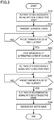
- FIG. 3 is a flowchart depicting part of processing performed by the ultrasonic sensor 100.
- the processing in Fig. 3 is realized by a program being executed by the control circuit 101 (refer to Fig. 1 ) of the ultrasonic sensor 100.
- part or all of the processing may be executed by a central processing unit (CPU) or other hardware.
- CPU central processing unit
- step S10 the control circuit 101 puts the path 109 (refer to Fig. 2 ) into the non-conductive state by driving the semiconductor element 107 (refer to Fig. 2 ).
- step S12 the control circuit 101 applies an alternating-current voltage to the transmission region 50A of the piezoelectric element 200 and causes an ultrasonic wave to be transmitted from the transmission region 50A.
- step S20 the control circuit 101 determines whether a predetermined period of time (for example, several microseconds to several milliseconds) has elapsed since the alternating-current voltage was applied to the transmission region 50A. In the case where the control circuit 101 determines that the predetermined period of time has elapsed since the alternating-current voltage was applied to the transmission region 50A (YES in step S20), the control circuit 101 switches the control to step S22. In the case where the determination is negative (NO in step S20), the control circuit 101 re-executes the processing of step S20.
- a predetermined period of time for example, several microseconds to several milliseconds
- step S22 the control circuit 101 stops application of the alternating-current voltage to the transmission region 50A.
- step S24 the control circuit 101 switches the path 109 from the non-conductive state to the conductive state by driving the semiconductor element 107.
- the reverberation signal output in accordance with the reverberant vibration is fed back to the transmission electrode from the reception region.
- the reverberant vibration of the ultrasonic sensor 100 is suppressed.
- step S30 the control circuit 101 determines whether a predetermined period of time (for example, several microseconds to several milliseconds) has elapsed since the path 109 was put into the conductive state. In the case where the control circuit 101 determines that the predetermined period of time has elapsed since the path 109 was put into the conductive state (YES in step S30), the control circuit 101 switches the control to step S32. In the case where the determination is negative (NO in step S30), the control circuit 101 re-executes the processing of step S30.
- a predetermined period of time for example, several microseconds to several milliseconds
- step S32 the control circuit 101 switches the path 109 from the conductive state to the non-conductive state by driving the semiconductor element 107.
- step S34 the control circuit 101 receives a reflected wave of the transmitted ultrasonic wave and outputs the reflected wave to the reception circuit 110 (refer to Fig. 1 ) as a voltage value.
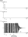
- Fig. 4 illustrates the output waveform of the ultrasonic sensor 100 in the case where the reverberant vibration is not suppressed.
- Fig. 5 illustrates the output waveform of the ultrasonic sensor 100 in the case where the reverberant vibration is suppressed.
- Graph (A) of Fig. 4 illustrates a control signal output from the control circuit 101 (refer to Fig. 1 ) to the signal generating circuit 104 (refer to Fig. 1 ).
- the signal generating circuit 104 Upon receiving the control signal, the signal generating circuit 104 applies an alternating-current voltage to the transmission region 50A (refer to Fig. 1 ) of the piezoelectric element 200.
- control circuit 101 outputs the control signal to the signal generating circuit 104 (refer to Fig. 1 ) in a period from a time T1 to a time T2.
- the signal generating circuit 104 applies an alternating-current voltage to the transmission region 50A.
- the control circuit 101 stops outputting the control signal to the signal generating circuit 104.
- the signal generating circuit 104 stops applying the alternating-current voltage to the transmission region 50A of the piezoelectric element 200.
- Graph (B) of Fig. 4 illustrates a control signal output from the control circuit 101 to the semiconductor element 107 (refer to Fig. 1 ).
- the control circuit 101 does not output the control signal to the semiconductor element 107 in the period from the start of control until the finish of control.
- the path 109 (refer to Fig. 1 ) of the reverberation signal is maintained in a non-conductive state and the reverberation signal is not fed back to the transmission region 50A.
- Graph (C) of Fig. 4 illustrates the output waveform of the ultrasonic sensor 100.
- the reverberation signal is not fed back and therefore the piezoelectric element 200 vibrates even after the time T2 at which application of the alternating-current voltage is stopped.
- a reflected wave received at a time T4 is buried in the reverberant vibration (refer to dotted line 301). Therefore the ultrasonic sensor 100 cannot detect the reflected wave.
- Graph (A) of Fig. 5 illustrates a control signal output from the control circuit 101 to the signal generating circuit 104.
- Graph (A) of Fig. 5 is the same as graph (A) of Fig. 4 and therefore description thereof will not be repeated.
- Graph (B) of Fig. 5 illustrates a control signal output from the control circuit 101 to the semiconductor element 107. More specifically, the control circuit 101 puts the path 109 in a non-conductive state after starting control until the time T2. The control circuit 101 puts the path 109 into the conductive state in the period from the time T2 until a time T3 by driving the semiconductor element 107. In other words, the ultrasonic sensor 100 feeds the reverberation signal output from the reception region 50B back to the transmission region 50A. The control circuit 101 puts the path 109 into the non-conductive state from the time T3 onwards.
- Graph (C) of Fig. 5 illustrates the output waveform of the ultrasonic sensor 100 in the case where the reverberant vibration is suppressed.
- the reverberation signal is fed back to the transmission region 50A in the period from the time T2 until the time T3, and as a result, the reverberant vibration is suppressed (refer to dotted line 303).
- the ultrasonic sensor 100 can detect the reflected wave received at the time T4.
- the ultrasonic sensor 100 can detect the reflected wave without waiting for the reverberant vibration to naturally subside. Therefore, the ultrasonic sensor 100 can detect closer objects than was previously possible and can improve the accuracy with which objects are detected and the accuracy with which distances are measured.
- Fig. 6 illustrates an example of the circuit configuration of the ultrasonic sensor 100X according to the comparative example.
- the ultrasonic sensor 100X includes a signal generating circuit 104, semiconductor elements 120 and 122, amplifiers 121A to 121C and 123A to 123C and a piezoelectric element 200X.
- the piezoelectric element 200X includes a transmission/reception electrode 10X, a monitoring electrode 20X, a common electrode 30X and a piezoelectric body 50X.
- the transmission/reception electrode 10X is provided with a terminal DRV.
- the monitoring electrode 20X is provided with a terminal MON.
- the common electrode 30X is provided with a terminal COM.
- the signal generating circuit 104 is connected to the terminal DRV and the terminal COM.
- the amplifiers 121A to 121C are connected in series between the terminal MON and the semiconductor element 120.
- the semiconductor element 120 is connected between the amplifier 121C and the terminal DRV.
- the semiconductor element 122 is connected to the terminal DRV and is connected in parallel with the semiconductor element 120.
- the amplifiers 123A to 123C are connected in series with the semiconductor element 122.
- the ultrasonic sensor 100X outputs a control signal to the signal generating circuit 104 and as a result an alternating-current voltage is applied between the terminal DRV and the terminal COM.
- the ultrasonic sensor 100X puts a path 126 into a non-conductive state by driving the semiconductor element 120 and puts a path 127 into a non-conductive state by driving the semiconductor element 122.
- the ultrasonic sensor 100X stops application of the alternating-current voltage and switches the path 126 from the non-conductive state to a conductive state.
- a reverberation signal which corresponds to a reverberant vibration of the piezoelectric element 200X is amplified by the amplifiers 121A to 121C and then fed back to the transmission/reception electrode 10X.
- the reverberant vibration is suppressed.
- the ultrasonic sensor 100X switches the path 126 from the conductive state to the non-conductive state and switches the path 127 from the non-conductive state to the conductive state.
- the ultrasonic sensor 100X Upon receiving a reflected wave of the ultrasonic wave, the ultrasonic sensor 100X amplifies a signal generated in accordance with the reflected wave with the amplifiers 123A to 123C and then outputs the amplified signal to a reception circuit.
- the monitoring electrode 20X which is for detecting the reverberant vibration, is formed separately from the transmission/reception electrode 10X, which is for transmitting and receiving an ultrasonic wave. Consequently, both a circuit configuration for feeding back the reverberation signal and a circuit configuration for receiving the reflected wave are necessary. More specifically, the semiconductor element 120, the amplifiers 121A to 121C and so forth are necessary as the circuit configuration for feeding back the reverberation signal. The semiconductor element 122, the amplifiers 123A to 123C and so forth are necessary as the circuit configuration for receiving the reflected wave. In other words, the ultrasonic sensor 100X needs two semiconductor elements 120 and 122 and six amplifiers 121A to 121C and 123A to 123C.
- an electrode for detecting the reverberant vibration and an electrode for receiving the ultrasonic wave are provided as a single reception electrode 20. Therefore, the ultrasonic sensor 100 can utilize the same circuit elements in the step of detecting the reverberant vibration and in the step of receiving a reflected wave. More specifically, the ultrasonic sensor 100 can realize both detection of the reverberant vibration and reception of the reflected wave with the same semiconductor element 107 and the same amplifier 108.
- an ultrasonic sensor 100C can realize both detection of the reverberant vibration and reception of the reflected wave with the same semiconductor element 107 and the same amplifier (amplifier 108, operational amplifier 141 and buffer circuit 113).
- the ultrasonic sensor 100 can realize suppression of the reverberant vibration with a simpler circuit configuration than the ultrasonic sensor 100X.
- the ultrasonic sensor 100 is reduced in size as a result of the circuit configuration of the ultrasonic sensor 100 being simpler.
- Fig. 7 illustrates noise signals generated by switching of semiconductor elements.
- Fig. 8 illustrates an output waveform of the ultrasonic sensor 100X (refer to Fig. 6 ) according to the comparative example.
- the ultrasonic sensor 100X puts the path 126 into the conductive state by driving the semiconductor element 120 and puts the path 127 into the non-conductive state by driving the semiconductor element 122 when suppressing the reverberant vibration.
- the ultrasonic sensor 100X puts the path 126 into the non-conductive state by driving the semiconductor element 120 and puts the path 127 into the conductive state by driving the semiconductor element 122 when receiving the reflected wave.
- Noise signals are generated due to the switching of the semiconductor elements 120 and 122. This noise signals are caused by the circuit being connected to different potentials, clock feed through of the semiconductor elements, charge injection of the semiconductor elements and so forth. The source of the noise signals will be described in more detail while referring to Fig. 7 .
- a semiconductor element M1 serving as a positive-channel metal oxide semiconductor (PMOS) transistor and a semiconductor element M2 serving as a negative-channel metal oxide semiconductor (NMOS) transistor are illustrated.
- Parasitic capacitances C1 and C2 are generated in the semiconductor element M1.
- Parasitic capacitances C3 and C4 are generated in the semiconductor element M2.
- the waveform of a control signal at position P1 is illustrated in graph (B) of Fig. 7 .
- This control signal is output by a control circuit CLK.
- the control signal is output to the semiconductor element M1 after being inverted by an element INV and is output to the semiconductor element M2 without being inverted.
- the semiconductor elements M1 and M2 are driven at times T11 and T12.
- Graph (C) of Fig. 7 illustrates changes in voltage that occur at position P2.
- Graph (D) of Fig. 7 illustrates changes in voltage that occur at position P3.
- so-called potential jumps (ringing) caused by the parasitic capacitances C1 to C4 occur at the times T11 and T12 when the semiconductor elements M1 and M2 are driven (refer to dotted lines 303).
- noise signals generated by the control circuit CLK pass through the parasitic capacitances C1 to C4 and flow into a signal line A-Z (refer to dotted lines 305).
- Noise signals generated by switching of the semiconductor elements are generated in the ultrasonic sensor 100X according to the comparative example.
- Graph (A) of Fig. 8 illustrates a control signal output from the ultrasonic sensor 100X to the signal generating circuit 104 (refer to Fig. 6 ).
- Graph (B) of Fig. 8 illustrates a control signal output from the ultrasonic sensor 100X to the semiconductor element 120.
- Graph (C) of Fig. 8 illustrates the output waveform of the ultrasonic sensor 100X.
- potential jumps are generated as noise signals at the times T2 and T3 at which the semiconductor element 120 is driven (refer to dotted lines 307 and 309).
- the strength of a reception signal generated by a reflected wave from a target is very low, and therefore the gain in the reception circuit is several thousand times to several tens of thousands of times. Therefore, even in the case where the noise signals themselves are weak, the noise signals will be amplified several thousand times to several tens of thousands of times.
- the amplified noise signals flow to the reception circuit 110 and appear in the output waveform.
- the ultrasonic sensor 100 does not require a semiconductor element for the reception circuit 110.
- a noise signal generated by switching of a semiconductor element is not generated in the reception circuit 110, the above-described problem does not occur.
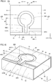
- Fig. 9 is a plan view illustrating the piezoelectric element 200.
- Fig. 10 is a perspective view illustrating the piezoelectric element 200.
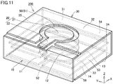
- Fig. 11 is a perspective view illustrating the piezoelectric element 200 and the internal structure thereof.
- Fig. 12 is a perspective view illustrating the transmission electrode 10, the reception electrode 20 and the common electrode 30 of the piezoelectric element 200.
- Fig. 13 is a sectional view looking in the direction of arrows and taken along line XIII-XIII in Fig. 9 .
- Fig. 9 is a plan view illustrating the piezoelectric element 200.
- Fig. 10 is a perspective view illustrating the piezoelectric element 200.
- Fig. 11 is a perspective view illustrating the piezoelectric element 200 and the internal structure thereof.
- Fig. 12 is a perspective view illustrating the transmission electrode 10, the reception electrode 20 and the common electrode 30 of the piezoelectric element 200.
- Fig. 13 is a sectional view looking
- Fig. 14 is a sectional view looking in the direction of arrows and taken along line XIV-XIV in Fig. 9 .
- Fig. 15 is a sectional view looking in the direction of arrows and taken along line XV-XV in Fig. 9 .
- the ultrasonic sensor 100 is configured such that the number of stacked layers of the piezoelectric element is larger in the transmission region 50A than in the reception region 50B.
- Arrows X, Y and Z are illustrated in Figs. 9 to 15 for convenience of explanation.
- the arrows X, Y and Z are perpendicular to each other.
- the arrangement relationships between the constituent parts are not necessarily limited to arrangement relationships indicated by the arrows X, Y and Z.
- the piezoelectric element 200 includes the transmission electrode 10, the reception electrode 20, the common electrode 30 and the piezoelectric body 50.
- the piezoelectric body 50 has a substantially rectangular parallelepiped outer shape (refer to Figs. 10 and 11 ) and the piezoelectric body 50 has an upper surface 51, side surfaces 52 to 55 and a lower surface 56.
- the upper surface 51 is a surface of the piezoelectric body 50 that is located on the arrow Z direction side and the lower surface 56 is a surface of the piezoelectric body 50 that is located on the opposite side to the arrow Z direction side.
- the side surfaces 52 and 54 are surfaces of the piezoelectric body 50 that are perpendicular to the arrow X direction and have a positional relationship of facing each other.
- the side surfaces 53 and 55 are surfaces of the piezoelectric body 50 that are perpendicular to the arrow Y direction and have a positional relationship of facing each other.
- the transmission electrode 10 includes a side wall portion 11, an upper surface portion 12 and middle portions 13 and 14 (refer to Fig. 12 ).
- the side wall portion 11, the upper surface portion 12 and the middle portions 13 and 14 each have a plate-like shape.
- the side wall portion 11 is arranged so as to face the side surface 52 of the piezoelectric body 50 (refer to Fig. 10 ) and contact the side surface 52.
- the side wall portion 11 has a surface shape that covers the entirety of the side surface 52 of the piezoelectric body 50 (refer to Figs. 9 , 14 and 15 ).
- the upper surface portion 12 is connected to an end portion of the side wall portion 11 on the arrow Z direction side (and on side in direction opposite to that of arrow Y) and is arranged on the upper surface 51 of the piezoelectric body 50.
- the upper surface portion 12 has a smaller width than the side wall portion 11, "width" referring to the dimension in the arrow Y direction.
- An end portion of the upper surface portion 12 in the direction opposite to that of the arrow Y has a flush relationship with the side surface 53 of the piezoelectric body 50.
- the terminal DRV is provided on the upper surface portion 12.
- a wiring line (not illustrated) is connected to the terminal DRV.
- the upper surface portion 12 and the middle portions 13 and 14 have a parallel positional relationship with each other and the middle portions 13 and 14 are located closer to the side in the opposite direction to the arrow Z than the upper surface portion 12.
- the middle portion 13 is located between the upper surface portion 12 and the middle portion 14.
- the middle portion 13 and the middle portion 14 face each other with a space therebetween.
- the middle portions 13 and 14 are parts of the transmission electrode 10 that are arranged inside the piezoelectric body 50 and cannot be seen when the piezoelectric element 200 is in its completed state (refer to Fig. 10 ). This will be described in detail later, but a middle portion 33 of the common electrode 30 is arranged between the middle portion 13 and the middle portion 14 (refer to Figs. 13 to 15 etc.).
- Hollow portions 13H and 14H ( Fig. 12 ), which have a circular shape, are respectively provided inside the middle portions 13 and 14.
- the sizes (outer diameters) of the hollow portions 13H and 14H are larger than the size (outer diameter) of a disk portion 21 of the reception electrode 20.
- the positions of the hollow portions 13H and 14H correspond to the position of the disk portion 21 of the reception electrode 20.
- the hollow portions 13H and 14H are arranged at positions so as to not overlap a projected image of the disk portion 21 when then disk portion 21 of the reception electrode 20 is projected in a direction opposite to that of the arrow Z (refer to Figs. 13 and 15 ).
- Cut out portions 13T and 14T are also respectively provided inside the middle portions 13 and 14.
- the cut out portions 13T and 14T are arranged so as to extend from the side where the hollow portions 13H and 14H are located to the side where the side surface 52 of the piezoelectric body 50 is located (in direction opposite to that of the arrow X).
- the positions of the cut out portions 13T and 14T correspond to the position of an extending portion 22 of the reception electrode 20.
- end portions of the middle portions 13 and 14 in a direction opposite to that of the arrow X are connected to the side wall portion 11.
- end portions of the middle portions 13 and 14 in the arrow X direction are not connected to a side wall portion 31 of the common electrode 30 and are separated from the side wall portion 31.
- the reception electrode 20 includes a disk portion 21 and an extending portion 22 and has a plate-like shape on the whole (refer to Fig. 12 ).
- the extending portion 22 has a rectangular outer shape and is shaped so as to extend from an outer edge of the disk portion 21 toward the outside.
- the extending portion 22 is provided with the terminal REC.
- a wiring line (not illustrated) is connected to the terminal REC.
- the reception electrode 20 is arranged on the upper surface 51 such that the disk portion 21 is located in the center of the upper surface 51 of the piezoelectric body 50.
- the extending portion 22 is arranged so as to extend from the side where the disk portion 21 is located toward the side where the side surface 52 of the piezoelectric body 50 is located (in direction opposite to that of arrow X).
- the common electrode 30 includes a side wall portion 31, an upper surface portion 32, a middle portion 33 and a lower surface portion 34 (refer to Fig. 12 ).
- the side wall portion 31, the upper surface portion 32, the middle portion 33 and the lower surface portion 34 each have a plate-like shape.
- the side wall portion 31 is arranged so as to face the side surface 54 of the piezoelectric body 50 (refer to Fig. 10 ) and contact the side surface 54.
- the side wall portion 31 has a surface shape that covers the entirety of the side surface 54 of the piezoelectric body 50 (refer to Figs. 9 , 14 and 15 ).
- the lower surface portion 34 is arranged so as to face the lower surface 56 of the piezoelectric body 50 and so as to contact the lower surface 56.
- the lower surface portion 34 has a surface shape that covers the entirety of the lower surface 56 of the piezoelectric body 50.
- the upper surface portion 32 is connected to an end portion of the side wall portion 31 on the arrow Z direction side and is arranged on the upper surface 51 of the piezoelectric body 50.
- the width of the upper surface portion 32 is equal to the width of the upper surface 51 of the piezoelectric body 50, "width" referring to the dimension in the arrow Y direction.
- the two end portions of the upper surface portion 32 in the arrow Y direction respectively have a flush relationship with the side surface 53 and 55 of the piezoelectric body 50.
- the terminal COM is provided on the upper surface portion 32.
- a wiring line (not illustrated) is connected to the terminal COM.
- the upper surface portion 32, the middle portion 33 and the lower surface portion 34 have a parallel positional relationship with each other, and the middle portion 33 and the lower surface portion 34 are located closer to the side in the opposite direction to the arrow Z than the upper surface portion 32.
- the middle portion 33 is located between the upper surface portion 32 and the lower surface portion 34.
- the middle portion 33 is part of the common electrode 30 that is arranged inside the piezoelectric body 50 and cannot be seen when the piezoelectric element 200 is in its completed state (refer to Fig. 10 ).
- Hollow portions 32H and 33H (refer to Fig. 12 ), which have a circular shape, are respectively provided inside the upper surface portion 32 and the middle portion 33.
- the sizes (outer diameters) of the hollow portions 32H and 33H are larger than the size (outer diameter) of the disk portion 21 of the reception electrode 20.
- the positions of the hollow portions 32H and 33H correspond to the position of the disk portion 21 of the reception electrode 20.
- the disk portion 21 of the reception electrode 20 is arranged inside the hollow portion 32H (refer to Fig. 10 ).
- the hollow portion 33H is arranged at a position so as to not overlap a projected image of the disk portion 21 when the disk portion 21 of the reception electrode 20 is projected in a direction opposite to that of the arrow Z (refer to Figs. 13 and 15 ).
- Cut out portions 32T and 33T are also respectively provided inside the upper surface portion 32 and the middle portion 33.
- the cut out portions 32T and 33T are arranged so as to extend from the side where the hollow portions 32H and 33H are located toward the side where the side surface 52 of the piezoelectric body 50 is located (in direction opposite to that of the arrow X).
- the positions of the cut out portions 32T and 33T correspond to the position of the extending portion 22 of the reception electrode 20.
- the extending portion 22 of the reception electrode 20 is arranged inside the cut out portion 32T (refer to Fig. 10 ).
- a recessed portion 32F is provided in a part of the upper surface portion 32 located in the opposite direction to that of the arrow Y.
- the recessed portion 32F is a part for allowing arrangement of the upper surface portion 12 of the transmission electrode 10.
- end portions of the upper surface portion 32, the middle portion 33 and the lower surface portion 34 in the arrow X direction are connected to the side wall portion 31.
- end portions of the upper surface portion 32, the middle portion 33 and the lower surface portion 34 in the direction opposite to that of the arrow X are not connected to the side wall portion 11 of the transmission electrode 10 and are separated from the side wall portion 11.
- the transmission region 50A and the reception region 50B are formed inside the piezoelectric body 50.
- the transmission region 50A has a four-layer structure made up of piezoelectric layers A1 to A4.
- the white arrows in Figs. 13 to 15 indicate the polarization directions of the piezoelectric layers.
- the piezoelectric layers A1 to A4 are manufactured by interposing the middle portion 13 of the transmission electrode 10, the middle portion 33 of the common electrode 30 and the middle portion 14 of the transmission electrode 10 between four piezoelectric layers, each of which is composed of a thin piezoelectric ceramic material having a strip-like shape, stacking these layers on top of one another and then firing the layers so that the layers become integrated with each other.
- the piezoelectric layers A1 to A4 are electrically connected in parallel with each other by the transmission electrode 10 and the common electrode 30.
- the reception region 50B has a one-layer structure made up of a piezoelectric layer B1.
- the piezoelectric layer B1 is manufactured by stacking four piezoelectric layers, each of which is composed of a thin piezoelectric ceramic material having a strip-like shape, on top of one another without interposing any electrodes between the layers and then firing the layers so that the layers become integrated with each other.
- the lower surface portion 34 of the common electrode 30 has a shape that extends across both the transmission region 50A and the reception region 50B.
- the upper surface portion 12 of the transmission electrode 10 faces the lower surface portion 34 of the common electrode 30 with the transmission region 50A including the piezoelectric layers A1 to A4 interposed therebetween.
- the disk portion 21 of the reception electrode 20 faces the lower surface portion 34 of the common electrode 30 with the reception region 50B including the piezoelectric layer B1 interposed therebetween.
- a region of the piezoelectric body 50 located between the upper surface portion 12 of the transmission electrode 10 and the lower surface portion 34 of the common electrode 30 functions as the transmission region 50A and a region of the piezoelectric body 50 located between the disk portion 21 of the reception electrode 20 and the lower surface portion 34 of the common electrode 30 functions as the reception region 50B.
- the transmission region 50A and the reception region 50B are formed at positions that are adjacent to each other in the X-Y plane direction.
- the ultrasonic sensor 100 puts the path 109 between the transmission electrode 10 and the reception electrode 20 into a conductive state by driving the semiconductor element 107, which is electrically connected to the transmission electrode 10 and the reception electrode 20, after stopping application of an alternating-current voltage.
- the ultrasonic sensor 100 feeds a reverberation signal, which is output from the reception region 50B in accordance with a reverberant vibration generated after transmission of the ultrasonic wave, back to the transmission electrode 10.
- the ultrasonic sensor 100 can detect a reflected wave without waiting for the reverberant vibration to subside, the ultrasonic sensor 100 can detect a reflected wave from an object even in the case where the object is close to the ultrasonic sensor 100.
- an electrode for detecting the reverberant vibration and an electrode for receiving the ultrasonic wave are provided as a single reception electrode 20. Therefore, the ultrasonic sensor 100 can utilize the same circuit elements in a detection circuit for detecting a reverberant vibration and a reception circuit for receiving a reflected wave. Thus, the circuit configuration of the ultrasonic sensor 100 becomes simpler and the ultrasonic sensor 100 is reduced in size.
- the ultrasonic sensor 100 can suppress a signal/noise (S/N) ratio.
- the semiconductor element 107 is not limited to being a transistor.
- the semiconductor element 107 may be formed of a diode as illustrated in Fig. 24 , which will be described later.
- the reverberation signal is higher than a threshold voltage (for example, forward voltage) at which the diode is driven and an output signal that accompanies a reflected wave of an ultrasonic wave is lower than the threshold voltage.
- the reverberation signal is fed back to the transmission electrode 10 as a voltage in the step of suppressing the reverberant vibration, but the output signal is not fed back to the transmission electrode 10 in the step of receiving a reflected wave of an ultrasonic wave. Therefore, the same effect as with the ultrasonic sensor 100 according to the first embodiment can be obtained in this case as well.
- FIG. 16 illustrates an example of the circuit configuration of the ultrasonic sensor 100A.
- the ultrasonic sensor 100A differs from the ultrasonic sensor 100 according to the first embodiment in that the ultrasonic sensor 100A further includes a phase adjuster 111. Except for the phase adjuster 111, the rest of the configuration is the same as that described above and therefore description thereof will not be repeated.
- the ultrasonic sensor 100A includes the signal generating circuit 104, the semiconductor element 107, the amplifier 108, the reception circuit 110, the phase adjuster 111 and the piezoelectric element 200.
- the phase adjuster 111 is electrically connected to the semiconductor element 107 and the amplifier 108 along the path 109.
- the reverberation signal may be shifted more than expected due to circuit characteristics, the surrounding environment (for example, temperature) and so forth.
- the phase adjuster 111 adjusts the phase of the reverberation signal from the reception region 50B in order that the reverberant vibration can be optimally suppressed and feeds the phase-adjusted reverberation signal back to the transmission electrode 10.
- the size of the phase shift applied by the phase adjuster 111 may be determined in advance at the design stage or may be changed in accordance with the surrounding environment (for example, temperature etc.), the circuit characteristics and so forth.
- the ultrasonic sensor 100A feeds back a phase-adjusted reverberation signal to the transmission electrode 10. Consequently, the ultrasonic sensor 100A can suppress the reverberant vibration with greater certainty.
- FIG. 17 illustrates an example of the circuit configuration of the ultrasonic sensor 100B.
- the ultrasonic sensor 100B differs from the ultrasonic sensor 100A according to the second embodiment in that the ultrasonic sensor 100B further includes a buffer circuit 113. Apart from the buffer circuit 113, the rest of the configuration is the same as that described above and therefore description thereof will not be repeated.
- the ultrasonic sensor 100B includes the signal generating circuit 104, the semiconductor element 107, the amplifier 108, the reception circuit 110, the phase adjuster 111, the buffer circuit 113 and the piezoelectric element 200.
- the buffer circuit 113 is electrically connected to the phase adjuster 111 and the semiconductor element 107 along the path 109.
- the ultrasonic sensor 100B prevents a noise signal from flowing from the transmission electrode 10 into the reception circuit 110 via the path 109. As a result, the SN ratio can be reduced in the reception circuit 110.
- the path 109 which is provided in order to reduce the reverberant vibration
- a path 114 which is provided in order to receive an ultrasonic wave
- the ultrasonic sensor 100B can prevent a noise signal from flowing into the reception circuit 110.
- Fig. 18 illustrates a parasitic capacitance generated in the ultrasonic sensor 100B.
- the present inventors newly discovered that a parasitic capacitance 115 is generated between the transmission electrode 10 and the reception electrode 20. As far as the present inventors are aware, there are no prior art documents that disclose that the parasitic capacitance 115 is generated between the transmission electrode 10 and the reception electrode 20. The present inventors think that the reason this has not been discovered to date is that an ultrasonic sensor having a three terminal structure made up of the transmission electrode 10, the reception electrode 20 and the common electrode 30 is in itself new.
- a reverberation signal output from the transmission region 50A or a reverberation signal fed back from the reception region 50B may flow into the path 109 via the parasitic capacitance 115. Consequently, there is a possibility that the piezoelectric element 200 may undergo abnormal oscillation.
- An ultrasonic sensor 100C according to a fourth embodiment can prevent such an abnormal oscillation as described below.
- Fig. 19 illustrates an example of the circuit configuration of the ultrasonic sensor 100C.
- the ultrasonic sensor 100C differs from the ultrasonic sensor 100B according to the third embodiment in that the ultrasonic sensor 100C further includes a filter circuit 140, which functions as an I/V conversion circuit, and a protection circuit 160. Apart from the filter circuit 140 and the protection circuit 160, the rest of the configuration is the same that as described above and therefore description thereof will not be repeated.
- the ultrasonic sensor 100C includes the signal generating circuit 104, the semiconductor element 107, the amplifier 108, the reception circuit 110, the phase adjuster 111, the buffer circuit 113, the filter circuit 140 and the protection circuit 160.
- the filter circuit 140 filters out a signal of a frequency band that causes the ultrasonic sensor 100C to undergo abnormal oscillation.
- the filter circuit 140 is provided along the path 109.
- the filter circuit 140 can filter out a noise signal that flows into the path 109 from the parasitic capacitance 115 and can prevent the ultrasonic sensor 100C from undergoing abnormal oscillation.
- the filter circuit 140 is formed as an I/V conversion circuit made up of an operational amplifier 141, a resistor 143 and a capacitor 145. It is sufficient that the filter circuit 140 have a function of cutting a specific frequency by converting a current into a voltage.
- a charge amplifier may be used instead of the operational amplifier 141.
- An inverting input terminal of the operational amplifier 141 is electrically connected to the reception electrode 20 (terminal REC).
- a non-inverting input terminal of the operational amplifier 141 is grounded.
- An output terminal of the operational amplifier 141 is electrically connected to the amplifier 108.
- the resistor 143 is electrically connected to the inverting input terminal of the operational amplifier 141 and to the output terminal of the operational amplifier 141.
- the capacitor 145 is electrically connected to the inverting input terminal of the operational amplifier 141 and to the output terminal of the operational amplifier 141.
- the operational amplifier 141, the resistor 143 and the capacitor 145 are connected in parallel with each other.
- the filter circuit 140 functions as a low pass filter based on the ratio between the parasitic capacitance 115 and the capacitance of the capacitor 145.
- this ratio is expressed as a value obtained by dividing the parasitic capacitance 115 by the capacitance of the capacitor 145.
- the capacitance of the capacitor 145 is preferably larger than the parasitic capacitance 115.
- the filter circuit 140 can reduce the gain response to a signal component of a frequency band that causes abnormal oscillation and can make the ultrasonic sensor 100C operate more stably.
- the filter circuit 140 is illustrated as being an I/V conversion circuit that functions as a low pass filter, but the filter circuit 140 is not limited to being an I/V conversion circuit.
- the filter circuit 140 may be a band pass filter or may be a charge amplifier circuit.
- a band pass filter would be configured to allow a frequency band that contains the resonant frequency of the piezoelectric element 200 to pass therethrough.
- the band pass filter would be configured to cut signals of frequency bands outside the resonant frequency of the piezoelectric element 200.
- FIG. 20 illustrates examples of the circuit configurations of ultrasonic sensors 100Y and 100Z according to comparative examples.
- the ultrasonic sensor 100Y includes a voltage follower circuit 170 instead of the filter circuit 140 (refer to Fig. 19 ).
- the voltage follower circuit 170 includes an operational amplifier 171.
- the noise signal flows directly to the inverting input terminal of the operational amplifier 171.
- the ultrasonic sensor 100Y will undergo abnormal oscillation due to this noise signal.
- the ultrasonic sensor 100Z includes an inverter amplification circuit 180 instead of the filter circuit 140 (refer to Fig. 19 ).
- the inverter amplification circuit 180 includes a capacitor 181, an operational amplifier 183 and resistors 184 and 185.
- a noise signal flows through the parasitic capacitance 115 of the ultrasonic sensor 100Z, the noise signal flows directly to the inverting input terminal of the operational amplifier 183.
- the ultrasonic sensor 100Z will undergo abnormal oscillation due to this noise signal.
- the protection circuit 160 will be described while referring to Fig. 19 again.
- a voltage that is equal to or higher than the power supply voltage may be applied to the operational amplifier 141 depending on the resonance characteristics of the ultrasonic sensor 100C.
- the protection circuit 160 prevents such an excessive voltage from being applied to the operational amplifier 141.
- the protection circuit 160 includes diodes 161 and 163.
- the cathode of the diode 161 is connected to the path 109.
- the anode of the diode 161 is grounded.
- the cathode of the diode 163 is grounded.
- the anode of the diode 163 is connected to the path 109.
- the ultrasonic sensor 100C does not necessarily have to be provided with the protection circuit 160.
- Fig. 21 illustrates simulation results obtained in a case where an abnormal oscillation occurs and simulation results obtained in a case where an abnormal oscillation does not occur.
- graphs (A1) and (B1) of Fig. 21 illustrate a control signal output from the ultrasonic sensor 100C to the signal generating circuit 104.
- graphs (A2) and (B2) of Fig. 21 illustrate a control signal output from the ultrasonic sensor 100C to the semiconductor element 107.
- Graph (A3) of Fig. 21 illustrates the output waveform of the ultrasonic sensor 100C in the case where the parasitic capacitance 115 is assumed to be 50 pF (pico-Farads) and the capacitance of the capacitor 145 is assumed to be 10 pF.
- a noise signal that passes through the parasitic capacitance 115 appears as an output waveform in the period from the time T2 to the time T3 in which the reverberant vibration is suppressed (refer to dotted line 311).
- the ultrasonic sensor 100C undergoes abnormal oscillation from the time T3 onwards due to the noise signal. Therefore, the ultrasonic sensor 100C cannot detect the reflected wave received at the time T4 (refer to dotted line 313).
- Graph (B3) of Fig. 21 illustrates the output waveform of the ultrasonic sensor 100C in the case where the parasitic capacitance 115 is assumed to be 50 pF and the capacitance of the capacitor 145 is assumed to be 100 pF.
- a noise signal from the parasitic capacitance 115 does not appear as an output waveform in the period from the time T2 to the time T3 in which the reverberant vibration is suppressed (refer to dotted line 311). Therefore, the ultrasonic sensor 100C does not undergo abnormal oscillation from the time T3 onwards and is able to detect the reflected wave received at the time T4.
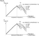
- Fig. 22 illustrates the relationship between the frequency of a signal flowing through the ultrasonic sensor 100C when the reverberant vibration is being suppressed and the gain of the ultrasonic sensor 100C with respect to the signal (hereafter also referred to as "open loop characteristics").
- Graph (A) of Fig. 22 illustrates open loop characteristics obtained when the parasitic capacitance 115 is made to be 0.1 pF, 1 pF, 10 pF and 100 pF for a case where the filter circuit 140 is not provided.
- the gain is 0 dB or more in a frequency band outside the resonant frequency (refer to dotted line 321). A signal of this frequency band is the cause of the abnormal oscillation.
- Graph (B) of Fig. 22 illustrates open loop characteristics obtained when the parasitic capacitance 115 is made to be 0.1 pF, 1 pF, 10 pF and 100 pF for a case where the filter circuit 140 is provided.
- the capacitance of the capacitor 145 of the filter circuit 140 is 100 pF.
- the gain of the signal in the frequency band outside the resonant frequency is suppressed by the filter circuit 140.
- the ultrasonic sensor 100C includes the filter circuit 140 that filters out the signal of the frequency band that causes the ultrasonic sensor 100C to undergo abnormal oscillation.
- the ultrasonic sensor 100C can prevent the occurrence of abnormal oscillation.
- FIG. 23 illustrates differences in reverberation time with respect to temperature in the ultrasonic sensor 100C according to the fourth embodiment and in the ultrasonic sensor 100Z according to the comparative example.
- the ultrasonic sensor 100C according to the fourth embodiment has smaller variations in reverberation time with respect to temperature than the ultrasonic sensor 100Z according to the comparative example.
- the reason for these results is thought to be that the input of the I/V conversion circuit is ideally in a virtual short circuit state and therefore a signal corresponding to the vibration velocity of the ultrasonic sensor can be extracted without being affected by a damping capacitance of the ultrasonic sensor and there is unlikely to be an effect due the temperature characteristics of the damping capacitance.
- FIG. 24 illustrates an example of the circuit configuration of the ultrasonic sensor 100D.
- the semiconductor element 107 is formed by a transistor.
- the semiconductor element 107 is formed by diodes 191 and 192. Apart from the semiconductor element 107, the rest of the configuration is the same as that described above and therefore description thereof will not be repeated.
- the diodes 191 and 192 are provided along the path 109 and are connected in parallel with each other.
- the cathode of the diode 191 is connected to the amplifier 108.
- the anode of the diode 191 is connected to the terminal DRV.
- the cathode of the diode 192 is connected to the terminal DRV.
- the anode of the diode 192 is connected to the amplifier 108.
- the semiconductor element 107 is formed of the diodes 191 and 192.
- the reverberation signal is higher than a threshold voltage (for example, forward voltage) at which the diodes 191 and 192 are driven and an output signal that accompanies a reflected wave of an ultrasonic wave is lower than the threshold voltage. Therefore, the reverberation signal is fed back to the transmission electrode 10 as a voltage in the step of suppressing the reverberant vibration, but the output signal is not fed back to the transmission electrode 10 in the step of receiving a reflected wave of an ultrasonic wave. Therefore, the same effect as with the ultrasonic sensor 100 according to the first embodiment can be obtained in this case as well.
- a threshold voltage for example, forward voltage
- FIG. 25 illustrates an example of the circuit configuration of the ultrasonic sensor 100E.
- the ultrasonic sensor 100E according to the sixth embodiment is further provided with a step up transformer 106 along the electrical path 109 that connects the transmission electrode 10 and the reception electrode 20 in the ultrasonic sensor 100 according to the first embodiment. More specifically, the step up transformer 106 is connected to a position on the terminal DRV side of the transmission electrode 10, that is, in front of the transmission electrode 10. Apart from the step up transformer 106, the rest of the configuration is the same as that described above and therefore description thereof will not be repeated.
- the step up transformer 106 includes a primary coil and a secondary coil.
- the primary coil of the step up transformer 106 is connected to the signal generating circuit 104 and the semiconductor element 107.
- the secondary coil of the step up transformer 106 is connected to the terminal DRV.
- the ratio between the primary coil side voltage and the secondary coil side voltage is 1:10, for example.
- the ultrasonic sensor 100F according to the seventh embodiment differs from the ultrasonic sensor 100A according to the first embodiment in that the ultrasonic sensor 100F has a plurality of operation modes having different detection distances.
- the ultrasonic sensor 100F sequentially switches between the plurality of operation modes having different detection distances and controls the piezoelectric element 200 (refer to Fig. 1 ) using control conditions corresponding to the current operation mode.
- the ultrasonic sensor 100F can detect an object in any location. It is sufficient that the ultrasonic sensor 100F have at least two operation modes.
- the hardware configuration and so forth of the ultrasonic sensor 100F according to the seventh embodiment is the same as that of the ultrasonic sensor 100 according to the first embodiment and therefore description thereof will not be repeated hereafter.
- Fig. 26 is a flowchart that depicts part of the processing executed by the ultrasonic sensor 100F according to the seventh embodiment.
- the processing in Fig. 26 is realized by a program being executed by the control circuit 101 (refer to Fig. 1 ), which is for controlling the ultrasonic sensor 100F.
- part or all of the processing may be executed by a CPU or other hardware.
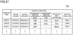
- step S2 the control circuit 101 reads control information 124 illustrated in Fig. 27.
- Fig. 27 illustrates the content of the control information 124.
- the control information 124 is stored in advance in a storage region of the control circuit 101, for example.
- control conditions of the piezoelectric element 200 (refer to Fig. 1 ) are assigned in accordance with detection distances of the ultrasonic sensor 100F for the operation modes of the ultrasonic sensor 100F.
- step S4 the control circuit 101 obtains control conditions corresponding to the current operation mode of the ultrasonic sensor 100F from the control information 124.
- step S10 the control circuit 101 puts the path 109 (refer to Fig. 2 ) into the non-conductive state by driving the semiconductor element 107 (refer to Fig. 2 ).
- step S12A the control circuit 101 applies an alternating-current voltage to the transmission region 50A of the piezoelectric element 200 (refer to Fig. 1 ) on the basis of the control conditions obtained in step S4. More specifically, a driving voltage of the piezoelectric element 200 and a driving frequency of the piezoelectric element 200 are stipulated in the control conditions obtained in step S4 and the control circuit 101 drives the piezoelectric element 200 at the driving voltage and the driving frequency. Thus, an ultrasonic wave is caused to be transmitted from the transmission region 50A of the piezoelectric element 200.
- step S20 the control circuit 101 determines whether a predetermined period of time (for example, several microseconds to several milliseconds) has elapsed since the alternating-current voltage was applied to the transmission region 50A. In the case where the control circuit 101 determines that the predetermined period of time has elapsed since the alternating-current voltage was applied to the transmission region 50A (YES in step S20), the control circuit 101 switches the control to step S22. In the case where the determination is negative (NO in step S20), the control circuit 101 re-executes the processing of step S20.
- a predetermined period of time for example, several microseconds to several milliseconds
- step S22 the control circuit 101 stops application of the alternating-current voltage to the transmission region 50A of the piezoelectric element 200.
- step S23 the control circuit 101 determines whether to suppress the reverberant vibration on the basis of the control conditions obtained in step S4. More specifically, a suppression mode indicating whether to enable suppression of the reverberant vibration is stipulated in the control conditions obtained in step S4. In the case where the suppression mode stipulated in the control conditions obtained in step S4 is ON, the control circuit 101 determines to suppress the reverberant vibration. In the case where the suppression mode in the control conditions obtained in step S4 is OFF, the control circuit 101 determines not to suppress the reverberant vibration. The control circuit 101 switches the control to step S24 in the case where the control circuit 101 determines to suppress the reverberant vibration (YES in step S23). The control circuit 101 switches the control to step S34A in the case where the determination is negative (NO in step S23).
- step S24 the control circuit 101 switches the path 109 from the non-conductive state to the conductive state by driving the semiconductor element 107.
- the reverberation signal output in accordance with the reverberant vibration is fed back to the transmission electrode 10 (refer to Fig. 2 ) from the reception region 50B (refer to Fig. 2 ) of the piezoelectric element 200.
- the reverberant vibration of the ultrasonic sensor 100F is suppressed.
- step S30A the control circuit 101 determines whether a predetermined period of time had elapsed since the path 109 was put into the conductive state.
- the predetermined period of time is stipulated in the control conditions obtained in step S4. That is, the control circuit 101 puts the path 109 into the conductive state for a period of time stipulated in the control conditions obtained in step S4.
- the control circuit 101 switches the control to step S32.
- the control circuit 101 re-executes the processing of step S30A.
- step S32 the control circuit 101 switches the path 109 from the conductive state to the non-conductive state by driving the semiconductor element 107.
- step S34A the control circuit 101 controls the reception region 50B of the piezoelectric element 200 on the basis of the control conditions obtained in step S4.
- a waiting time from transmission of the ultrasonic wave until reception of the reflected wave and gain of the reception signal output in response to reception of the reflected wave are stipulated in the control conditions obtained in step S4.
- the control circuit 101 outputs a reflected wave received in the period from transmission of the ultrasonic wave until the waiting time elapses to the reception circuit 110 (refer to Fig. 1 ) as a voltage value that corresponds to the gain.
- the control circuit 101 switches the control to step S40 in response to the waiting time from transmission of the ultrasonic wave elapsing.
- step S40 the control circuit 101 determines whether control processing according to this embodiment has been executed for all the operation modes of the ultrasonic sensor 100F. In the case where the control circuit 101 determines that the control processing according to this embodiment has been executed for all the operation modes of the ultrasonic sensor 100F (YES in step S40), the control circuit 101 ends the control processing according to this embodiment. The control circuit 101 switches the control to step S50 in the case where the determination is negative (NO in step S40).
- step S50 the control circuit 101 switches the operation mode of the ultrasonic sensor 100F from the current operation mode to another operation mode.
- steps S40 and S50 the processing illustrated in Fig. 26 is repeated a number of times equal to the number of operation modes of the ultrasonic sensor 100F.
- the ultrasonic sensor 100F sequentially switches between the plurality of operation modes having different detection distances and controls the piezoelectric element 200 using the control conditions corresponding to the current operation mode.
- the range of distances that can be detected is increased.
- the ultrasonic sensor 100F can detect an object in any location.
- the ultrasonic sensor 100G according to the eighth embodiment differs from the ultrasonic sensor 100F according to the seventh embodiment in that the ultrasonic sensor 100G has at least an operation mode for detecting a short distance (first operation mode) (hereafter, also referred to as "short-distance mode”) and an operation mode for detecting a long distance (second operation mode) (hereafter, also referred to as "long-distance mode").
- first operation mode hereafter, also referred to as "short-distance mode”
- second operation mode hereafter, also referred to as "long-distance mode
- Fig. 28 is a flowchart that depicts part of the processing executed by the ultrasonic sensor 100G according to the eighth embodiment.
- the processing in Fig. 28 is realized by a program being executed by the control circuit 101 (refer to Fig. 1 ), which is for controlling the ultrasonic sensor 100G.
- part or all of the processing may be executed by a CPU or other hardware.
- step S23A Since the processing of steps other than step S23A is the same as that described in Fig. 3 , description thereof will not be repeated hereafter.
- step S23A the control circuit 101 determines whether the operation mode of the ultrasonic sensor 100G is the short-distance mode.
- the operation mode of the ultrasonic sensor 100G is arbitrarily set by a user, for example.
- the control circuit 101 switches the control to step S24.
- the control circuit 101 switches the control to step S34 in the case where the determination is negative (NO in step S23A).
- step S23A the control circuit 101 executes the processing of steps S24 to S32, which is for suppressing the reverberant vibration, in the case where the operation mode of the ultrasonic sensor 100G is the short-distance mode.
- the control circuit 101 executes processing to feed the reverberation signal back to the transmission electrode 10 of the piezoelectric element 200 (refer to Fig. 1 ).
- the control circuit 101 does not execute the processing of steps S24 to S32 for suppressing the reverberant vibration.
- the control circuit 101 stops the processing of feeding the reverberation signal back to the transmission electrode 10 of the piezoelectric element 200.
- the ultrasonic sensor 100G does not execute the processing for suppressing the reverberant vibration in the case where the operation mode is the long-distance mode. Thus, power consumption of the ultrasonic sensor 100G is suppressed.
Landscapes
- Engineering & Computer Science (AREA)
- Physics & Mathematics (AREA)
- Radar, Positioning & Navigation (AREA)
- Remote Sensing (AREA)
- General Physics & Mathematics (AREA)
- Computer Networks & Wireless Communication (AREA)
- Acoustics & Sound (AREA)
- Signal Processing (AREA)
- Mechanical Engineering (AREA)
- Measurement Of Velocity Or Position Using Acoustic Or Ultrasonic Waves (AREA)
- Transducers For Ultrasonic Waves (AREA)
Abstract
Description
- The present disclosure relates to an ultrasonic sensor that includes a piezoelectric element, and more specifically, relates to control of an ultrasonic sensor.
- Ultrasonic sensors that include piezoelectric elements are known. An ultrasonic sensor causes a piezoelectric element to vibrate by applying an alternating-current voltage to a piezoelectric element, and as a result transmits an ultrasonic wave. The ultrasonic sensor detects an object on the basis of reception of an ultrasonic wave reflected by the object.
- A vibration remains in the ultrasonic sensor after transmission of the ultrasonic wave. The ultrasonic sensor may erroneously detect this vibration (hereafter, also referred to as a "reverberant vibration") as a reflected wave. In recent years, technologies for suppressing reverberant vibrations have been disclosed. For example, Japanese Unexamined Patent Application Publication No.
2009-4916 - Patent Document 1: Japanese Unexamined Patent Application Publication No.
2009-4916 - The ultrasonic wave output device disclosed in
Patent Document 1 is formed of a detection part that detects a reverberant vibration and a transmission/reception part that transmits/receives ultrasonic waves. The ultrasonic wave output device generates a signal for suppressing a reverberant vibration in accordance with a reverberant vibration detected by the detection part. After that, the ultrasonic wave output device suppresses the reverberant vibration by feeding the generated signal back to the transmission/reception part. Since the detection part for detecting a reverberant vibration is additionally provided in the ultrasonic wave output device, a circuit configuration for feeding the signal for suppressing the reverberant vibration back to the transmission/reception part is required. Consequently, the circuit configuration becomes more complex. - The present disclosure was made in order to solve the above-described problem and an object of a certain aspect thereof is to provide an ultrasonic sensor that can suppress a reverberant vibration with a simpler circuit configuration than has been possible to date. An object of another aspect thereof is to provide a control method for an ultrasonic sensor that can suppress a reverberant vibration with a simpler circuit configuration than has previously been possible.
- According to a certain aspect of the present invention, an ultrasonic sensor is provided that includes a piezoelectric element. The piezoelectric element includes: a flat-plate-shaped piezoelectric body that includes a transmission region that is for transmitting an ultrasonic wave in response to having an alternating-current voltage applied thereto and a reception region that is for receiving a reflected wave of the ultrasonic wave; a common electrode that is provided in the transmission region and the reception region; a transmission electrode that is arranged so as to face the common electrode with the transmission region interposed therebetween and that is provided in the transmission region; and a reception electrode that is arranged so as to face the common electrode with the reception region interposed therebetween and that is provided in the reception region. The ultrasonic sensor further includes a semiconductor element that is electrically connected to the transmission electrode and the reception electrode and switches an electrical path extending between the transmission electrode and the reception electrode between a conductive state and a non-conductive state. The semiconductor element preferably puts the path into the conductive state after application of the alternating-current voltage is stopped, and as a result a reverberation signal, which is output from the reception region in accordance with a reverberant vibration of the ultrasonic wave, is fed back to the transmission electrode.
- The semiconductor element preferably switches the path from the conductive state to the non-conductive state after the reverberation signal has been fed back to the transmission electrode.
- The ultrasonic sensor preferably further includes an amplifier that is connected in series with the semiconductor element along the path. The amplifier amplifies the reverberation signal and outputs the amplified reverberation signal to the transmission electrode.
- The ultrasonic sensor preferably further includes an I/V conversion circuit that convert a current into a voltage. The I/V conversion circuit is provided along the path.
- The I/V conversion circuit preferably filters a signal of a frequency band that causes the ultrasonic sensor to undergo abnormal oscillation.
- The I/V conversion circuit preferably includes an operational amplifier and a capacitor. An inverting input terminal of the operational amplifier is electrically connected to the reception electrode. An output terminal of the operational amplifier is electrically connected to the amplifier. The capacitor is electrically connected to the inverting input terminal and the output terminal.
- The ultrasonic sensor preferably further includes a reception circuit that is electrically connected to the I/V conversion circuit.
- The ultrasonic sensor preferably has a plurality of operation modes having different detection distances from each other. Control conditions of the piezoelectric element are associated in advance with the plurality of operation modes in accordance with the detection distances. The ultrasonic sensor sequentially switches between the plurality of operation modes and controls the piezoelectric element using the control conditions corresponding to a current operation mode.
- The ultrasonic sensor preferably has a first operation mode and a second operation mode that has a longer detection distance than the first operation mode. The ultrasonic sensor executes processing to feed the reverberation signal back to the transmission electrode in the first operation mode and does not execute processing to feed the reverberation signal back to the transmission electrode in the second operation mode.
- The ultrasonic sensor preferably further includes a step up transformer that is provided along the path.
- According to another aspect of the present invention, a control method for an ultrasonic sensor is provided. The ultrasonic sensor includes a piezoelectric element. The piezoelectric element includes: a flat-plate-shaped piezoelectric body that includes a transmission region that is for transmitting an ultrasonic wave in response to having an alternating-current voltage applied thereto and a reception region that is for receiving a reflected wave of the ultrasonic wave; a common electrode that is provided in the transmission region and the reception region; a transmission electrode that is arranged so as to face the common electrode with the transmission region interposed therebetween and that is provided in the transmission region; and a reception electrode that is arranged so as to face the common electrode with the reception region interposed therebetween and that is provided in the reception region. The ultrasonic sensor further includes a semiconductor element that is electrically connected to the transmission electrode and the reception electrode and switches an electrical path extending between the transmission electrode and the reception electrode between a conductive state and a non-conductive state. The control method includes: a step of putting the path into the non-conductive state; a step of applying an alternating-current voltage to the transmission region after the path has been put into the non-conductive state; and a step of feeding a reverberation signal, which is output from the reception region in accordance with a reverberant vibration of the ultrasonic wave, back to the transmission electrode by putting the path into the conductive state after stopping application of the alternating-current voltage.
- According to a certain aspect of the present invention, a reverberant vibration can be suppressed with a simpler circuit configuration than was previously possible. The above-described object, other objects, features, aspects and advantages of the present invention will become clearer from the following detailed description of the present invention, which is to be understood while referring to the accompanying drawings.
-
- [
Fig. 1] Fig. 1 illustrates an example of the circuit configuration of an ultrasonic sensor according to a first embodiment. - [
Fig. 2] Fig. 2 is a conceptual diagram that schematically illustrates an example of operation of the ultrasonic sensor according to the first embodiment. - [
Fig. 3] Fig. 3 is a flowchart that depicts part of the processing executed by the ultrasonic sensor according to the first embodiment. - [
Fig. 4] Fig. 4 illustrates signals in the case where the ultrasonic sensor according to the first embodiment does not suppress a reverberant vibration. - [
Fig. 5] Fig. 5 illustrates signals in the case where the ultrasonic sensor according to the first embodiment does suppress a reverberant vibration. - [
Fig. 6] Fig. 6 illustrates an example of the circuit configuration of an ultrasonic sensor according to a comparative example. - [
Fig. 7] Fig. 7 illustrates noise signals generated by switching of semiconductor elements. - [
Fig. 8] Fig. 8 illustrates signals of the ultrasonic sensor according to the comparative example. - [
Fig. 9] Fig. 9 is a plan view illustrating a piezoelectric element according to the first embodiment. - [
Fig. 10] Fig. 10 is a perspective view illustrating the piezoelectric element according to the first embodiment. - [
Fig. 11] Fig. 11 is a perspective view illustrating the piezoelectric element according to the first embodiment and the internal structure thereof. - [
Fig. 12] Fig. 12 is a perspective view illustrating a transmission electrode, a reception electrode and a common electrode of the piezoelectric element according to the first embodiment. - [
Fig. 13] Fig. 13 is a sectional view looking in the direction of arrows and taken along line XIII-XIII inFig. 9 . - [
Fig. 14] Fig. 14 is a sectional view looking in the direction of arrows and taken along line XIV-XIV inFig. 9 . - [
Fig. 15] Fig. 15 is a sectional view looking in the direction of arrows and taken along line XV-XV inFig. 9 . - [
Fig. 16] Fig. 16 illustrates an example of the circuit configuration of an ultrasonic sensor according to a second embodiment. - [
Fig. 17] Fig. 17 illustrates an example of the circuit configuration of an ultrasonic sensor according to a third embodiment. - [
Fig. 18] Fig. 18 illustrates a parasitic capacitance generated in the ultrasonic sensor according to the third embodiment. - [
Fig. 19] Fig. 19 illustrates an example of the circuit configuration of an ultrasonic sensor according to a fourth embodiment. - [
Fig. 20] Fig. 20 illustrates examples of the circuit configurations of ultrasonic sensors according to comparative examples. - [
Fig. 21] Fig. 21 illustrates simulation results obtained in a case where an abnormal oscillation occurs and simulation results obtained in a case where an abnormal oscillation does not occur. - [
Fig. 22] Fig. 22 illustrates the relationship between the frequency of a signal flowing in an ultrasonic sensor when a reverberant vibration is suppressed and the gain of the ultrasonic sensor with respect to the signal. - [
Fig. 23] Fig. 23 illustrates differences in reverberation time with respect to temperature in an ultrasonic sensor according to the fourth embodiment and in the ultrasonic sensor according to the comparative example. - [
Fig. 24] Fig. 24 illustrates an example of the circuit configuration of an ultrasonic sensor according to a fifth embodiment. - [
Fig. 25] Fig. 25 illustrates an example of the circuit configuration of an ultrasonic sensor according to a sixth embodiment. - [
Fig. 26] Fig. 26 is a flowchart that depicts part of the processing executed by an ultrasonic sensor according to a seventh embodiment. - [
Fig. 27] Fig. 27 illustrates the content of control information in the seventh embodiment. - [
Fig. 28] Fig. 28 is a flowchart that depicts part of the processing executed by an ultrasonic sensor according to an eighth embodiment. - Hereafter, embodiments of the present invention will be described while referring to the drawings. In the following description, identical components and constituent elements will be denoted by the same symbols. The names and functions of these components and constituent elements will also be the same. Therefore, detailed description of these components and constituent elements will not be repeated. In addition, the embodiments or modifications described hereafter may be appropriately selectively combined with each other.
- An
ultrasonic sensor 100 according to a first embodiment will be described while referring toFig. 1. Fig. 1 illustrates an example of the circuit configuration of theultrasonic sensor 100. - The
ultrasonic sensor 100 is installed in a vehicle or a smartphone, for example. Theultrasonic sensor 100 measures the distance from itself to an object in accordance with the time taken from transmitting an ultrasonic wave until receiving a reflected wave. Alternatively, theultrasonic sensor 100 detects the existence of an object on the basis of reception of a reflected wave. - As illustrated in
Fig. 1 , theultrasonic sensor 100 includes acontrol circuit 101, amemory 102, asignal generating circuit 104, apower source 105, asemiconductor element 107, anamplifier 108, areception circuit 110 and apiezoelectric element 200. - The
control circuit 101 is a microcomputer, for example. Thesemiconductor element 107 is a transistor, for example. Thecontrol circuit 101 switches anelectrical path 109, which extends between atransmission electrode 10 and areception electrode 20, between a conductive state and a non-conductive state by driving thesemiconductor element 107. Furthermore, thecontrol circuit 101 reads out data stored in thememory 102 and outputs an appropriate control signal for driving theultrasonic sensor 100 to thesignal generating circuit 104. Thepower source 105 outputs a direct-current voltage of 12 V, for example, to thesignal generating circuit 104. Thesignal generating circuit 104 generates an alternating-current voltage from the direct-current voltage on the basis of the control signal output from thecontrol circuit 101. The alternating-current voltage is supplied to thepiezoelectric element 200 after being boosted by an amplification circuit (not illustrated) as required. - The
piezoelectric element 200 includes thetransmission electrode 10, thereception electrode 20, acommon electrode 30 and apiezoelectric body 50. Thepiezoelectric element 200 has the shape of a flat plate, for example. Thetransmission electrode 10 is provided with a terminal DRV. Thereception electrode 20 is provided with a terminal REC. Thecommon electrode 30 is provided with a terminal COM. Thepiezoelectric element 200 has a three terminal structure made up of the terminal DRV, the terminal REC and the terminal COM. The terminal COM is grounded, but does not necessarily have to be grounded. - The
piezoelectric body 50 includes atransmission region 50A, which is for transmitting an ultrasonic wave, and areception region 50B, which is for receiving a reflected wave of the ultrasonic wave. Thetransmission electrode 10 is arranged so as to face thecommon electrode 30 with thetransmission region 50A interposed therebetween and is electrically connected to thetransmission region 50A. Thereception electrode 20 is arranged so as to face thecommon electrode 30 with thereception region 50B interposed therebetween and is electrically connected to thereception region 50B. Thecommon electrode 30 is electrically connected to thetransmission region 50A and thereception region 50B. - The
amplifier 108 is connected in series with thereception electrode 20 and thesemiconductor element 107. As an example, theamplifier 108 is an inverter amplification circuit formed of a resistor and an operational amplifier. - The
reception circuit 110 detects a received wave signal, which is generated in thereception region 50B in response to reception of a reflected wave, as a voltage value and outputs the voltage value to thecontrol circuit 101. - Although the
ultrasonic sensor 100 having a three terminal structure is illustrated inFig. 1 , theultrasonic sensor 100 may instead have a structure including four or more terminals. In this case, for example, a configuration may be adopted in which an electrode, which is a different electrode from thetransmission electrode 10 and thereception electrode 20, is arranged so as to face thecommon electrode 30 with thepiezoelectric body 50 interposed therebetween. This electrode is electrically connected to thepiezoelectric body 50. - Operation of the
ultrasonic sensor 100 according to this embodiment will be described while referring toFig. 2. Fig. 2 is a conceptual diagram schematically illustrating an example of operation of theultrasonic sensor 100. To facilitate easy understanding of the description, thecontrol circuit 101, thememory 102, thepower source 105 and thereception circuit 110 illustrated inFig. 1 are not illustrated inFig. 2 . - As illustrated in
Fig. 2 , theultrasonic sensor 100 according to this embodiment sequentially executes step (A) of transmitting an ultrasonic wave, step (B) of suppressing a reverberant vibration generated by transmission of the ultrasonic wave and step (C) of receiving a reflected wave of the ultrasonic wave. Hereafter, steps (A) to (C) will be described in turn. - In step (A), the
control circuit 101 puts thepath 109 into the non-conductive state by driving thesemiconductor element 107. Next, thecontrol circuit 101 outputs a control command to thesignal generating circuit 104, and as a result, thesignal generating circuit 104 applies an alternating-current voltage to thetransmission region 50A of thepiezoelectric element 200. The period of the alternating-current voltage is preferably equal to the resonant frequency of thetransmission region 50A of thepiezoelectric element 200. As a result of the alternating-current voltage being applied to thetransmission region 50A, thetransmission region 50A starts to vibrate due to the inverse piezoelectric effect and transmits an ultrasonic wave into the air, for example. - In step (B), the
control circuit 101 stops application of the alternating-current voltage to thetransmission region 50A once a predetermined period of time (for example, several microseconds to several milliseconds) has elapsed since transmission of the ultrasonic waves started. At this time, the vibration of thetransmission region 50A does not immediately subside. In other words, thetransmission region 50A continues to vibrate for a while after application of the alternating-current voltage has stopped. This vibration (i.e., a reverberant vibration) affects thereception region 50B and thereception region 50B resonates with thetransmission region 50A. - The
control circuit 101 switches thepath 109 from the non-conductive state to the conductive state after stopping application of the alternating-current voltage. Thus, a closed circuit is formed which is made up of thetransmission electrode 10, thetransmission region 50A, thecommon electrode 30, thereception region 50B, thereception electrode 20 and thepath 109 in this order. As described above, thetransmission region 50A and thereception region 50B vibrate due to the reverberant vibration. The reverberant vibration of thetransmission region 50A and thereception region 50B is suppressed by supplying a signal of an appropriate phase so as to cancel out the reverberant vibration. For example, in this embodiment, the reverberant vibration is suppressed in a short period of time by feeding back to the transmission terminal a voltage whose phase is shifted by 180° with respect to the vibration velocity of the reverberant vibration propagating along thepath 109. In other words, the reverberant vibration of thepiezoelectric element 200 is suppressed by feeding back, as a voltage, to the transmission electrode 10 a reverberation signal output from thereception region 50B in accordance with the reverberant vibration. - The
amplifier 108 preferably amplifies the reverberation signal output from thereception region 50B and outputs the amplified reverberation signal to thetransmission electrode 10. The amplification ratio of the reverberation signal may be determined in advance at the design stage or may be changed in accordance with the magnitude of the alternating-current voltage applied to thetransmission region 50A. - In step (C), the
control circuit 101 switches thepath 109 from the conductive state to the non-conductive state after the reverberation signal has been fed back to thetransmission electrode 10. Thus, thereception region 50B is able to receive an ultrasonic wave reflected by an object. As a result, theultrasonic sensor 100 can accurately detect a reflected wave. Thereception region 50B vibrates as a result of receiving the ultrasonic wave and outputs a signal generated by the piezoelectric effect to thecontrol circuit 101 as a voltage value. - A control structure of the
ultrasonic sensor 100 will be described while referring toFig. 3. Fig. 3 is a flowchart depicting part of processing performed by theultrasonic sensor 100. The processing inFig. 3 is realized by a program being executed by the control circuit 101 (refer toFig. 1 ) of theultrasonic sensor 100. In another aspect of the present invention, part or all of the processing may be executed by a central processing unit (CPU) or other hardware. - In step S10, the
control circuit 101 puts the path 109 (refer toFig. 2 ) into the non-conductive state by driving the semiconductor element 107 (refer toFig. 2 ). - In step S12, the
control circuit 101 applies an alternating-current voltage to thetransmission region 50A of thepiezoelectric element 200 and causes an ultrasonic wave to be transmitted from thetransmission region 50A. - In step S20, the
control circuit 101 determines whether a predetermined period of time (for example, several microseconds to several milliseconds) has elapsed since the alternating-current voltage was applied to thetransmission region 50A. In the case where thecontrol circuit 101 determines that the predetermined period of time has elapsed since the alternating-current voltage was applied to thetransmission region 50A (YES in step S20), thecontrol circuit 101 switches the control to step S22. In the case where the determination is negative (NO in step S20), thecontrol circuit 101 re-executes the processing of step S20. - In step S22, the
control circuit 101 stops application of the alternating-current voltage to thetransmission region 50A. - In step S24, the
control circuit 101 switches thepath 109 from the non-conductive state to the conductive state by driving thesemiconductor element 107. Thus, the reverberation signal output in accordance with the reverberant vibration is fed back to the transmission electrode from the reception region. As a result, the reverberant vibration of theultrasonic sensor 100 is suppressed. - In step S30, the
control circuit 101 determines whether a predetermined period of time (for example, several microseconds to several milliseconds) has elapsed since thepath 109 was put into the conductive state. In the case where thecontrol circuit 101 determines that the predetermined period of time has elapsed since thepath 109 was put into the conductive state (YES in step S30), thecontrol circuit 101 switches the control to step S32. In the case where the determination is negative (NO in step S30), thecontrol circuit 101 re-executes the processing of step S30. - In step S32, the
control circuit 101 switches thepath 109 from the conductive state to the non-conductive state by driving thesemiconductor element 107. - In step S34, the
control circuit 101 receives a reflected wave of the transmitted ultrasonic wave and outputs the reflected wave to the reception circuit 110 (refer toFig. 1 ) as a voltage value. - The output of the
ultrasonic sensor 100 in the case where the reverberant vibration is suppressed and the output of theultrasonic sensor 100 in the case where the reverberant vibration is not suppressed will be compared while referring toFigs. 4 and5 .Fig. 4 illustrates the output waveform of theultrasonic sensor 100 in the case where the reverberant vibration is not suppressed.Fig. 5 illustrates the output waveform of theultrasonic sensor 100 in the case where the reverberant vibration is suppressed. - Graph (A) of
Fig. 4 illustrates a control signal output from the control circuit 101 (refer toFig. 1 ) to the signal generating circuit 104 (refer toFig. 1 ). Upon receiving the control signal, thesignal generating circuit 104 applies an alternating-current voltage to thetransmission region 50A (refer toFig. 1 ) of thepiezoelectric element 200. - More specifically, the
control circuit 101 outputs the control signal to the signal generating circuit 104 (refer toFig. 1 ) in a period from a time T1 to a time T2. As a result, thesignal generating circuit 104 applies an alternating-current voltage to thetransmission region 50A. From the time T2, thecontrol circuit 101 stops outputting the control signal to thesignal generating circuit 104. As a result, thesignal generating circuit 104 stops applying the alternating-current voltage to thetransmission region 50A of thepiezoelectric element 200. - Graph (B) of
Fig. 4 illustrates a control signal output from thecontrol circuit 101 to the semiconductor element 107 (refer toFig. 1 ). As illustrated in graph (B) ofFig. 4 , thecontrol circuit 101 does not output the control signal to thesemiconductor element 107 in the period from the start of control until the finish of control. In other words, the path 109 (refer toFig. 1 ) of the reverberation signal is maintained in a non-conductive state and the reverberation signal is not fed back to thetransmission region 50A. - Graph (C) of
Fig. 4 illustrates the output waveform of theultrasonic sensor 100. In the control example ofFig. 4 , the reverberation signal is not fed back and therefore thepiezoelectric element 200 vibrates even after the time T2 at which application of the alternating-current voltage is stopped. A reflected wave received at a time T4 is buried in the reverberant vibration (refer to dotted line 301). Therefore theultrasonic sensor 100 cannot detect the reflected wave. - Graph (A) of
Fig. 5 illustrates a control signal output from thecontrol circuit 101 to thesignal generating circuit 104. Graph (A) ofFig. 5 is the same as graph (A) ofFig. 4 and therefore description thereof will not be repeated. - Graph (B) of
Fig. 5 illustrates a control signal output from thecontrol circuit 101 to thesemiconductor element 107. More specifically, thecontrol circuit 101 puts thepath 109 in a non-conductive state after starting control until the time T2. Thecontrol circuit 101 puts thepath 109 into the conductive state in the period from the time T2 until a time T3 by driving thesemiconductor element 107. In other words, theultrasonic sensor 100 feeds the reverberation signal output from thereception region 50B back to thetransmission region 50A. Thecontrol circuit 101 puts thepath 109 into the non-conductive state from the time T3 onwards. - Graph (C) of
Fig. 5 illustrates the output waveform of theultrasonic sensor 100 in the case where the reverberant vibration is suppressed. The reverberation signal is fed back to thetransmission region 50A in the period from the time T2 until the time T3, and as a result, the reverberant vibration is suppressed (refer to dotted line 303). Thus, theultrasonic sensor 100 can detect the reflected wave received at the time T4. - By suppressing the reverberant vibration in this way, the
ultrasonic sensor 100 can detect the reflected wave without waiting for the reverberant vibration to naturally subside. Therefore, theultrasonic sensor 100 can detect closer objects than was previously possible and can improve the accuracy with which objects are detected and the accuracy with which distances are measured. - The
ultrasonic sensor 100 according to the first embodiment and anultrasonic sensor 100X according to a comparative example will be compared while referring toFig. 6. Fig. 6 illustrates an example of the circuit configuration of theultrasonic sensor 100X according to the comparative example. - First, the circuit configuration of the
ultrasonic sensor 100X according to the comparative example will be described. As illustrated inFig. 6 , theultrasonic sensor 100X includes asignal generating circuit 104,semiconductor elements amplifiers 121A to 121C and 123A to 123C and apiezoelectric element 200X. - The
piezoelectric element 200X includes a transmission/reception electrode 10X, amonitoring electrode 20X, acommon electrode 30X and apiezoelectric body 50X. The transmission/reception electrode 10X is provided with a terminal DRV. Themonitoring electrode 20X is provided with a terminal MON. Thecommon electrode 30X is provided with a terminal COM. - The
signal generating circuit 104 is connected to the terminal DRV and the terminal COM. Theamplifiers 121A to 121C are connected in series between the terminal MON and thesemiconductor element 120. Thesemiconductor element 120 is connected between theamplifier 121C and the terminal DRV. Thesemiconductor element 122 is connected to the terminal DRV and is connected in parallel with thesemiconductor element 120. Theamplifiers 123A to 123C are connected in series with thesemiconductor element 122. - Next, operation of the
ultrasonic sensor 100X according to the comparative example will be described while referring toFig. 6 . At the time of transmission of an ultrasonic wave, theultrasonic sensor 100X outputs a control signal to thesignal generating circuit 104 and as a result an alternating-current voltage is applied between the terminal DRV and the terminal COM. At this time, theultrasonic sensor 100X puts apath 126 into a non-conductive state by driving thesemiconductor element 120 and puts apath 127 into a non-conductive state by driving thesemiconductor element 122. - Next, the
ultrasonic sensor 100X stops application of the alternating-current voltage and switches thepath 126 from the non-conductive state to a conductive state. Thus, a reverberation signal, which corresponds to a reverberant vibration of thepiezoelectric element 200X is amplified by theamplifiers 121A to 121C and then fed back to the transmission/reception electrode 10X. As a result, the reverberant vibration is suppressed. - Next, the
ultrasonic sensor 100X switches thepath 126 from the conductive state to the non-conductive state and switches thepath 127 from the non-conductive state to the conductive state. Upon receiving a reflected wave of the ultrasonic wave, theultrasonic sensor 100X amplifies a signal generated in accordance with the reflected wave with theamplifiers 123A to 123C and then outputs the amplified signal to a reception circuit. - As described above, in the
ultrasonic sensor 100X according to the comparative example, themonitoring electrode 20X, which is for detecting the reverberant vibration, is formed separately from the transmission/reception electrode 10X, which is for transmitting and receiving an ultrasonic wave. Consequently, both a circuit configuration for feeding back the reverberation signal and a circuit configuration for receiving the reflected wave are necessary. More specifically, thesemiconductor element 120, theamplifiers 121A to 121C and so forth are necessary as the circuit configuration for feeding back the reverberation signal. Thesemiconductor element 122, theamplifiers 123A to 123C and so forth are necessary as the circuit configuration for receiving the reflected wave. In other words, theultrasonic sensor 100X needs twosemiconductor elements amplifiers 121A to 121C and 123A to 123C. - In contrast, in the
ultrasonic sensor 100 according to the first embodiment, an electrode for detecting the reverberant vibration and an electrode for receiving the ultrasonic wave are provided as asingle reception electrode 20. Therefore, theultrasonic sensor 100 can utilize the same circuit elements in the step of detecting the reverberant vibration and in the step of receiving a reflected wave. More specifically, theultrasonic sensor 100 can realize both detection of the reverberant vibration and reception of the reflected wave with thesame semiconductor element 107 and thesame amplifier 108. Similarly, anultrasonic sensor 100C according to a fourth embodiment, which will be described later, can realize both detection of the reverberant vibration and reception of the reflected wave with thesame semiconductor element 107 and the same amplifier (amplifier 108,operational amplifier 141 and buffer circuit 113). - Thus, the
ultrasonic sensor 100 can realize suppression of the reverberant vibration with a simpler circuit configuration than theultrasonic sensor 100X. Theultrasonic sensor 100 is reduced in size as a result of the circuit configuration of theultrasonic sensor 100 being simpler. - Another advantage of the
ultrasonic sensor 100 according to the first embodiment will be described while referring toFigs. 7 and8 .Fig. 7 illustrates noise signals generated by switching of semiconductor elements.Fig. 8 illustrates an output waveform of theultrasonic sensor 100X (refer toFig. 6 ) according to the comparative example. - As described in
Fig. 6 , theultrasonic sensor 100X puts thepath 126 into the conductive state by driving thesemiconductor element 120 and puts thepath 127 into the non-conductive state by driving thesemiconductor element 122 when suppressing the reverberant vibration. Theultrasonic sensor 100X puts thepath 126 into the non-conductive state by driving thesemiconductor element 120 and puts thepath 127 into the conductive state by driving thesemiconductor element 122 when receiving the reflected wave. - Noise signals are generated due to the switching of the
semiconductor elements Fig. 7 . - In the circuit example (A) of
Fig. 7 , a semiconductor element M1 serving as a positive-channel metal oxide semiconductor (PMOS) transistor and a semiconductor element M2 serving as a negative-channel metal oxide semiconductor (NMOS) transistor are illustrated. Parasitic capacitances C1 and C2 are generated in the semiconductor element M1. Parasitic capacitances C3 and C4 are generated in the semiconductor element M2. - The waveform of a control signal at position P1 is illustrated in graph (B) of
Fig. 7 . This control signal is output by a control circuit CLK. The control signal is output to the semiconductor element M1 after being inverted by an element INV and is output to the semiconductor element M2 without being inverted. In the example of the graph (B), the semiconductor elements M1 and M2 are driven at times T11 and T12. - Graph (C) of
Fig. 7 illustrates changes in voltage that occur at position P2. Graph (D) ofFig. 7 illustrates changes in voltage that occur at position P3. As illustrated in graphs (C) and (D), so-called potential jumps (ringing) caused by the parasitic capacitances C1 to C4 occur at the times T11 and T12 when the semiconductor elements M1 and M2 are driven (refer to dotted lines 303). In addition, noise signals generated by the control circuit CLK pass through the parasitic capacitances C1 to C4 and flow into a signal line A-Z (refer to dotted lines 305). - Noise signals generated by switching of the semiconductor elements are generated in the
ultrasonic sensor 100X according to the comparative example. Graph (A) ofFig. 8 illustrates a control signal output from theultrasonic sensor 100X to the signal generating circuit 104 (refer toFig. 6 ). Graph (B) ofFig. 8 illustrates a control signal output from theultrasonic sensor 100X to thesemiconductor element 120. Graph (C) ofFig. 8 illustrates the output waveform of theultrasonic sensor 100X. - As illustrated in graph (C) of
Fig. 8 , potential jumps are generated as noise signals at the times T2 and T3 at which thesemiconductor element 120 is driven (refer todotted lines 307 and 309). Typically, the strength of a reception signal generated by a reflected wave from a target is very low, and therefore the gain in the reception circuit is several thousand times to several tens of thousands of times. Therefore, even in the case where the noise signals themselves are weak, the noise signals will be amplified several thousand times to several tens of thousands of times. The amplified noise signals flow to thereception circuit 110 and appear in the output waveform. - In contrast, as illustrated in
Fig. 1 , theultrasonic sensor 100 according to the first embodiment does not require a semiconductor element for thereception circuit 110. Thus, since a noise signal generated by switching of a semiconductor element is not generated in thereception circuit 110, the above-described problem does not occur. - The structure of the
piezoelectric element 200 of theultrasonic sensor 100 will be described while referring toFigs. 9 to 15 .Fig. 9 is a plan view illustrating thepiezoelectric element 200.Fig. 10 is a perspective view illustrating thepiezoelectric element 200.Fig. 11 is a perspective view illustrating thepiezoelectric element 200 and the internal structure thereof.Fig. 12 is a perspective view illustrating thetransmission electrode 10, thereception electrode 20 and thecommon electrode 30 of thepiezoelectric element 200.Fig. 13 is a sectional view looking in the direction of arrows and taken along line XIII-XIII inFig. 9 .Fig. 14 is a sectional view looking in the direction of arrows and taken along line XIV-XIV inFig. 9 .Fig. 15 is a sectional view looking in the direction of arrows and taken along line XV-XV inFig. 9 . - In a multilayer ultrasonic sensor, as the number of stacked layers of the piezoelectric element increases, the acoustic pressure at the time of transmission of an ultrasonic wave increases, but the sensitivity at the time of reception of a reflected wave decreases. Conversely, as the number of stacked layers of the piezoelectric element decreases, the acoustic pressure at the time of transmission of an ultrasonic wave decreases, but the sensitivity at the time of reception of a reflected wave increases. Focusing on this point, the
ultrasonic sensor 100 is configured such that the number of stacked layers of the piezoelectric element is larger in thetransmission region 50A than in thereception region 50B. - Arrows X, Y and Z are illustrated in
Figs. 9 to 15 for convenience of explanation. The arrows X, Y and Z are perpendicular to each other. Hereafter, although the constituent parts of thepiezoelectric element 200 are sometimes described while referring to the arrows X, Y and Z, the arrangement relationships between the constituent parts (characteristics related to being perpendicular and parallel) are not necessarily limited to arrangement relationships indicated by the arrows X, Y and Z. - As illustrated in
Figs. 9 to 15 , thepiezoelectric element 200 includes thetransmission electrode 10, thereception electrode 20, thecommon electrode 30 and thepiezoelectric body 50. Thepiezoelectric body 50 has a substantially rectangular parallelepiped outer shape (refer toFigs. 10 and11 ) and thepiezoelectric body 50 has anupper surface 51, side surfaces 52 to 55 and alower surface 56. - The
upper surface 51 is a surface of thepiezoelectric body 50 that is located on the arrow Z direction side and thelower surface 56 is a surface of thepiezoelectric body 50 that is located on the opposite side to the arrow Z direction side. The side surfaces 52 and 54 are surfaces of thepiezoelectric body 50 that are perpendicular to the arrow X direction and have a positional relationship of facing each other. The side surfaces 53 and 55 are surfaces of thepiezoelectric body 50 that are perpendicular to the arrow Y direction and have a positional relationship of facing each other. - The
transmission electrode 10 includes aside wall portion 11, anupper surface portion 12 andmiddle portions 13 and 14 (refer toFig. 12 ). Theside wall portion 11, theupper surface portion 12 and themiddle portions side wall portion 11 is arranged so as to face theside surface 52 of the piezoelectric body 50 (refer toFig. 10 ) and contact theside surface 52. Theside wall portion 11 has a surface shape that covers the entirety of theside surface 52 of the piezoelectric body 50 (refer toFigs. 9 ,14 and 15 ). - The
upper surface portion 12 is connected to an end portion of theside wall portion 11 on the arrow Z direction side (and on side in direction opposite to that of arrow Y) and is arranged on theupper surface 51 of thepiezoelectric body 50. Theupper surface portion 12 has a smaller width than theside wall portion 11, "width" referring to the dimension in the arrow Y direction. An end portion of theupper surface portion 12 in the direction opposite to that of the arrow Y has a flush relationship with theside surface 53 of thepiezoelectric body 50. The terminal DRV is provided on theupper surface portion 12. A wiring line (not illustrated) is connected to the terminal DRV. - The
upper surface portion 12 and themiddle portions middle portions upper surface portion 12. Themiddle portion 13 is located between theupper surface portion 12 and themiddle portion 14. Themiddle portion 13 and themiddle portion 14 face each other with a space therebetween. Themiddle portions transmission electrode 10 that are arranged inside thepiezoelectric body 50 and cannot be seen when thepiezoelectric element 200 is in its completed state (refer toFig. 10 ). This will be described in detail later, but amiddle portion 33 of thecommon electrode 30 is arranged between themiddle portion 13 and the middle portion 14 (refer toFigs. 13 to 15 etc.). -
Hollow portions Fig. 12 ), which have a circular shape, are respectively provided inside themiddle portions hollow portions disk portion 21 of thereception electrode 20. The positions of thehollow portions disk portion 21 of thereception electrode 20. Thehollow portions disk portion 21 when thendisk portion 21 of thereception electrode 20 is projected in a direction opposite to that of the arrow Z (refer toFigs. 13 and 15 ). - Cut out
portions middle portions portions hollow portions side surface 52 of thepiezoelectric body 50 is located (in direction opposite to that of the arrow X). The positions of the cut outportions portion 22 of thereception electrode 20. As illustrated inFigs. 12 and14 , end portions of themiddle portions side wall portion 11. On the other hand, end portions of themiddle portions side wall portion 31 of thecommon electrode 30 and are separated from theside wall portion 31. - The
reception electrode 20 includes adisk portion 21 and an extendingportion 22 and has a plate-like shape on the whole (refer toFig. 12 ). The extendingportion 22 has a rectangular outer shape and is shaped so as to extend from an outer edge of thedisk portion 21 toward the outside. The extendingportion 22 is provided with the terminal REC. A wiring line (not illustrated) is connected to the terminal REC. - The
reception electrode 20 is arranged on theupper surface 51 such that thedisk portion 21 is located in the center of theupper surface 51 of thepiezoelectric body 50. The extendingportion 22 is arranged so as to extend from the side where thedisk portion 21 is located toward the side where theside surface 52 of thepiezoelectric body 50 is located (in direction opposite to that of arrow X). - The
common electrode 30 includes aside wall portion 31, anupper surface portion 32, amiddle portion 33 and a lower surface portion 34 (refer toFig. 12 ). Theside wall portion 31, theupper surface portion 32, themiddle portion 33 and thelower surface portion 34 each have a plate-like shape. Theside wall portion 31 is arranged so as to face theside surface 54 of the piezoelectric body 50 (refer toFig. 10 ) and contact theside surface 54. Theside wall portion 31 has a surface shape that covers the entirety of theside surface 54 of the piezoelectric body 50 (refer toFigs. 9 ,14 and 15 ). Thelower surface portion 34 is arranged so as to face thelower surface 56 of thepiezoelectric body 50 and so as to contact thelower surface 56. Thelower surface portion 34 has a surface shape that covers the entirety of thelower surface 56 of thepiezoelectric body 50. - The
upper surface portion 32 is connected to an end portion of theside wall portion 31 on the arrow Z direction side and is arranged on theupper surface 51 of thepiezoelectric body 50. The width of theupper surface portion 32 is equal to the width of theupper surface 51 of thepiezoelectric body 50, "width" referring to the dimension in the arrow Y direction. The two end portions of theupper surface portion 32 in the arrow Y direction respectively have a flush relationship with theside surface piezoelectric body 50. The terminal COM is provided on theupper surface portion 32. A wiring line (not illustrated) is connected to the terminal COM. - The
upper surface portion 32, themiddle portion 33 and thelower surface portion 34 have a parallel positional relationship with each other, and themiddle portion 33 and thelower surface portion 34 are located closer to the side in the opposite direction to the arrow Z than theupper surface portion 32. Themiddle portion 33 is located between theupper surface portion 32 and thelower surface portion 34. Themiddle portion 33 is part of thecommon electrode 30 that is arranged inside thepiezoelectric body 50 and cannot be seen when thepiezoelectric element 200 is in its completed state (refer toFig. 10 ). -
Hollow portions Fig. 12 ), which have a circular shape, are respectively provided inside theupper surface portion 32 and themiddle portion 33. The sizes (outer diameters) of thehollow portions disk portion 21 of thereception electrode 20. The positions of thehollow portions disk portion 21 of thereception electrode 20. Thedisk portion 21 of thereception electrode 20 is arranged inside thehollow portion 32H (refer toFig. 10 ). Thehollow portion 33H is arranged at a position so as to not overlap a projected image of thedisk portion 21 when thedisk portion 21 of thereception electrode 20 is projected in a direction opposite to that of the arrow Z (refer toFigs. 13 and 15 ). - Cut out
portions upper surface portion 32 and themiddle portion 33. The cut outportions hollow portions side surface 52 of thepiezoelectric body 50 is located (in direction opposite to that of the arrow X). The positions of the cut outportions portion 22 of thereception electrode 20. The extendingportion 22 of thereception electrode 20 is arranged inside the cut outportion 32T (refer toFig. 10 ). A recessedportion 32F is provided in a part of theupper surface portion 32 located in the opposite direction to that of the arrow Y. The recessedportion 32F is a part for allowing arrangement of theupper surface portion 12 of thetransmission electrode 10. - As illustrated in
Figs. 12 and14 , end portions of theupper surface portion 32, themiddle portion 33 and thelower surface portion 34 in the arrow X direction are connected to theside wall portion 31. On the other hand, end portions of theupper surface portion 32, themiddle portion 33 and thelower surface portion 34 in the direction opposite to that of the arrow X are not connected to theside wall portion 11 of thetransmission electrode 10 and are separated from theside wall portion 11. - As illustrated in
Figs. 13 to 15 , thetransmission region 50A and thereception region 50B are formed inside thepiezoelectric body 50. Thetransmission region 50A has a four-layer structure made up of piezoelectric layers A1 to A4. The white arrows inFigs. 13 to 15 indicate the polarization directions of the piezoelectric layers. - The piezoelectric layers A1 to A4 are manufactured by interposing the
middle portion 13 of thetransmission electrode 10, themiddle portion 33 of thecommon electrode 30 and themiddle portion 14 of thetransmission electrode 10 between four piezoelectric layers, each of which is composed of a thin piezoelectric ceramic material having a strip-like shape, stacking these layers on top of one another and then firing the layers so that the layers become integrated with each other. The piezoelectric layers A1 to A4 are electrically connected in parallel with each other by thetransmission electrode 10 and thecommon electrode 30. - The
reception region 50B has a one-layer structure made up of a piezoelectric layer B1. The piezoelectric layer B1 is manufactured by stacking four piezoelectric layers, each of which is composed of a thin piezoelectric ceramic material having a strip-like shape, on top of one another without interposing any electrodes between the layers and then firing the layers so that the layers become integrated with each other. - The
lower surface portion 34 of thecommon electrode 30 has a shape that extends across both thetransmission region 50A and thereception region 50B. Theupper surface portion 12 of thetransmission electrode 10 faces thelower surface portion 34 of thecommon electrode 30 with thetransmission region 50A including the piezoelectric layers A1 to A4 interposed therebetween. Thedisk portion 21 of thereception electrode 20 faces thelower surface portion 34 of thecommon electrode 30 with thereception region 50B including the piezoelectric layer B1 interposed therebetween. In other words, a region of thepiezoelectric body 50 located between theupper surface portion 12 of thetransmission electrode 10 and thelower surface portion 34 of thecommon electrode 30 functions as thetransmission region 50A and a region of thepiezoelectric body 50 located between thedisk portion 21 of thereception electrode 20 and thelower surface portion 34 of thecommon electrode 30 functions as thereception region 50B. As illustrated inFigs. 13 and 15 , in this embodiment, thetransmission region 50A and thereception region 50B are formed at positions that are adjacent to each other in the X-Y plane direction. - As described above, the
ultrasonic sensor 100 according to this embodiment puts thepath 109 between thetransmission electrode 10 and thereception electrode 20 into a conductive state by driving thesemiconductor element 107, which is electrically connected to thetransmission electrode 10 and thereception electrode 20, after stopping application of an alternating-current voltage. As a result, theultrasonic sensor 100 feeds a reverberation signal, which is output from thereception region 50B in accordance with a reverberant vibration generated after transmission of the ultrasonic wave, back to thetransmission electrode 10. - The closer an object is to the
ultrasonic sensor 100, the shorter the time taken from transmission of the ultrasonic wave until reception of the reflected wave. Since theultrasonic sensor 100 can detect a reflected wave without waiting for the reverberant vibration to subside, theultrasonic sensor 100 can detect a reflected wave from an object even in the case where the object is close to theultrasonic sensor 100. - In addition, in the
ultrasonic sensor 100 according to the first embodiment, an electrode for detecting the reverberant vibration and an electrode for receiving the ultrasonic wave are provided as asingle reception electrode 20. Therefore, theultrasonic sensor 100 can utilize the same circuit elements in a detection circuit for detecting a reverberant vibration and a reception circuit for receiving a reflected wave. Thus, the circuit configuration of theultrasonic sensor 100 becomes simpler and theultrasonic sensor 100 is reduced in size. - In particular, in this embodiment, there is no need to provide a semiconductor element for the
reception circuit 110. Therefore, a noise signal generated by switching of a semiconductor element can be suppressed in theultrasonic sensor 100. As a result, theultrasonic sensor 100 can suppress a signal/noise (S/N) ratio. - Although an example has been described in the above-described embodiment in which the
semiconductor element 107 is formed as a transistor that is driven by thecontrol circuit 101, thesemiconductor element 107 is not limited to being a transistor. For example, thesemiconductor element 107 may be formed of a diode as illustrated inFig. 24 , which will be described later. In this case, the reverberation signal is higher than a threshold voltage (for example, forward voltage) at which the diode is driven and an output signal that accompanies a reflected wave of an ultrasonic wave is lower than the threshold voltage. Therefore, the reverberation signal is fed back to thetransmission electrode 10 as a voltage in the step of suppressing the reverberant vibration, but the output signal is not fed back to thetransmission electrode 10 in the step of receiving a reflected wave of an ultrasonic wave. Therefore, the same effect as with theultrasonic sensor 100 according to the first embodiment can be obtained in this case as well. - An
ultrasonic sensor 100A according to a second embodiment will be described while referring toFig. 16. Fig. 16 illustrates an example of the circuit configuration of theultrasonic sensor 100A. - The
ultrasonic sensor 100A differs from theultrasonic sensor 100 according to the first embodiment in that theultrasonic sensor 100A further includes aphase adjuster 111. Except for thephase adjuster 111, the rest of the configuration is the same as that described above and therefore description thereof will not be repeated. - As illustrated in
Fig. 16 , theultrasonic sensor 100A includes thesignal generating circuit 104, thesemiconductor element 107, theamplifier 108, thereception circuit 110, thephase adjuster 111 and thepiezoelectric element 200. Thephase adjuster 111 is electrically connected to thesemiconductor element 107 and theamplifier 108 along thepath 109. - The reverberation signal may be shifted more than expected due to circuit characteristics, the surrounding environment (for example, temperature) and so forth.
- The
phase adjuster 111 adjusts the phase of the reverberation signal from thereception region 50B in order that the reverberant vibration can be optimally suppressed and feeds the phase-adjusted reverberation signal back to thetransmission electrode 10. The size of the phase shift applied by thephase adjuster 111 may be determined in advance at the design stage or may be changed in accordance with the surrounding environment (for example, temperature etc.), the circuit characteristics and so forth. - As described above, the
ultrasonic sensor 100A according to the second embodiment feeds back a phase-adjusted reverberation signal to thetransmission electrode 10. Consequently, theultrasonic sensor 100A can suppress the reverberant vibration with greater certainty. - An
ultrasonic sensor 100B according to a third embodiment will be described while referring toFig. 17. Fig. 17 illustrates an example of the circuit configuration of theultrasonic sensor 100B. - The
ultrasonic sensor 100B differs from theultrasonic sensor 100A according to the second embodiment in that theultrasonic sensor 100B further includes abuffer circuit 113. Apart from thebuffer circuit 113, the rest of the configuration is the same as that described above and therefore description thereof will not be repeated. - As illustrated in
Fig. 17 , theultrasonic sensor 100B includes thesignal generating circuit 104, thesemiconductor element 107, theamplifier 108, thereception circuit 110, thephase adjuster 111, thebuffer circuit 113 and thepiezoelectric element 200. Thebuffer circuit 113 is electrically connected to thephase adjuster 111 and thesemiconductor element 107 along thepath 109. - As a result of being provided with the
buffer circuit 113, theultrasonic sensor 100B prevents a noise signal from flowing from thetransmission electrode 10 into thereception circuit 110 via thepath 109. As a result, the SN ratio can be reduced in thereception circuit 110. - As described above, in the
ultrasonic sensor 100B according to the third embodiment, thepath 109, which is provided in order to reduce the reverberant vibration, and apath 114, which is provided in order to receive an ultrasonic wave, are electrically isolated from each other with greater certainty by thebuffer circuit 113. Thus, theultrasonic sensor 100B can prevent a noise signal from flowing into thereception circuit 110. - [New Knowledge] Knowledge newly discovered in the
ultrasonic sensor 100B according to the third embodiment will be described while referring toFig. 18. Fig. 18 illustrates a parasitic capacitance generated in theultrasonic sensor 100B. - The present inventors newly discovered that a
parasitic capacitance 115 is generated between thetransmission electrode 10 and thereception electrode 20. As far as the present inventors are aware, there are no prior art documents that disclose that theparasitic capacitance 115 is generated between thetransmission electrode 10 and thereception electrode 20. The present inventors think that the reason this has not been discovered to date is that an ultrasonic sensor having a three terminal structure made up of thetransmission electrode 10, thereception electrode 20 and thecommon electrode 30 is in itself new. - A reverberation signal output from the
transmission region 50A or a reverberation signal fed back from thereception region 50B may flow into thepath 109 via theparasitic capacitance 115. Consequently, there is a possibility that thepiezoelectric element 200 may undergo abnormal oscillation. Anultrasonic sensor 100C according to a fourth embodiment can prevent such an abnormal oscillation as described below. - The
ultrasonic sensor 100C according to the fourth embodiment will be described while referring toFig. 19. Fig. 19 illustrates an example of the circuit configuration of theultrasonic sensor 100C. - The
ultrasonic sensor 100C differs from theultrasonic sensor 100B according to the third embodiment in that theultrasonic sensor 100C further includes afilter circuit 140, which functions as an I/V conversion circuit, and aprotection circuit 160. Apart from thefilter circuit 140 and theprotection circuit 160, the rest of the configuration is the same that as described above and therefore description thereof will not be repeated. - As illustrated in
Fig. 19 , theultrasonic sensor 100C includes thesignal generating circuit 104, thesemiconductor element 107, theamplifier 108, thereception circuit 110, thephase adjuster 111, thebuffer circuit 113, thefilter circuit 140 and theprotection circuit 160. - The
filter circuit 140 filters out a signal of a frequency band that causes theultrasonic sensor 100C to undergo abnormal oscillation. Thefilter circuit 140 is provided along thepath 109. Thus, thefilter circuit 140 can filter out a noise signal that flows into thepath 109 from theparasitic capacitance 115 and can prevent theultrasonic sensor 100C from undergoing abnormal oscillation. - In the example in
Fig. 19 , thefilter circuit 140 is formed as an I/V conversion circuit made up of anoperational amplifier 141, aresistor 143 and acapacitor 145. It is sufficient that thefilter circuit 140 have a function of cutting a specific frequency by converting a current into a voltage. For example, a charge amplifier may be used instead of theoperational amplifier 141. - An inverting input terminal of the
operational amplifier 141 is electrically connected to the reception electrode 20 (terminal REC). A non-inverting input terminal of theoperational amplifier 141 is grounded. An output terminal of theoperational amplifier 141 is electrically connected to theamplifier 108. - The
resistor 143 is electrically connected to the inverting input terminal of theoperational amplifier 141 and to the output terminal of theoperational amplifier 141. Thecapacitor 145 is electrically connected to the inverting input terminal of theoperational amplifier 141 and to the output terminal of theoperational amplifier 141. Theoperational amplifier 141, theresistor 143 and thecapacitor 145 are connected in parallel with each other. - As a result of having this configuration, the
filter circuit 140 functions as a low pass filter based on the ratio between theparasitic capacitance 115 and the capacitance of thecapacitor 145. For example, this ratio is expressed as a value obtained by dividing theparasitic capacitance 115 by the capacitance of thecapacitor 145. The capacitance of thecapacitor 145 is preferably larger than theparasitic capacitance 115. Thus, thefilter circuit 140 can reduce the gain response to a signal component of a frequency band that causes abnormal oscillation and can make theultrasonic sensor 100C operate more stably. - In the example in
Fig. 19 , thefilter circuit 140 is illustrated as being an I/V conversion circuit that functions as a low pass filter, but thefilter circuit 140 is not limited to being an I/V conversion circuit. For example, thefilter circuit 140 may be a band pass filter or may be a charge amplifier circuit. A band pass filter would be configured to allow a frequency band that contains the resonant frequency of thepiezoelectric element 200 to pass therethrough. In other words, the band pass filter would be configured to cut signals of frequency bands outside the resonant frequency of thepiezoelectric element 200. - Circuit examples (A) and (B) in which there is a possibility that the ultrasonic sensor will undergo abnormal oscillation will be described while referring to
Fig. 20. Fig. 20 illustrates examples of the circuit configurations ofultrasonic sensors - As illustrated in the circuit example (A) of
Fig. 20 , theultrasonic sensor 100Y includes avoltage follower circuit 170 instead of the filter circuit 140 (refer toFig. 19 ). Thevoltage follower circuit 170 includes anoperational amplifier 171. When a noise signal flows through theparasitic capacitance 115 of theultrasonic sensor 100Y, the noise signal flows directly to the inverting input terminal of theoperational amplifier 171. There is a possibility that theultrasonic sensor 100Y will undergo abnormal oscillation due to this noise signal. - As illustrated in the circuit example (B) of
Fig. 20 , theultrasonic sensor 100Z includes aninverter amplification circuit 180 instead of the filter circuit 140 (refer toFig. 19 ). Theinverter amplification circuit 180 includes acapacitor 181, an operational amplifier 183 andresistors parasitic capacitance 115 of theultrasonic sensor 100Z, the noise signal flows directly to the inverting input terminal of the operational amplifier 183. There is a possibility that theultrasonic sensor 100Z will undergo abnormal oscillation due to this noise signal. - The
protection circuit 160 will be described while referring toFig. 19 again. A voltage that is equal to or higher than the power supply voltage may be applied to theoperational amplifier 141 depending on the resonance characteristics of theultrasonic sensor 100C. Theprotection circuit 160 prevents such an excessive voltage from being applied to theoperational amplifier 141. - The
protection circuit 160 includesdiodes diode 161 is connected to thepath 109. The anode of thediode 161 is grounded. The cathode of thediode 163 is grounded. The anode of thediode 163 is connected to thepath 109. Theultrasonic sensor 100C does not necessarily have to be provided with theprotection circuit 160. - Continuing to refer to
Fig. 19 , simulation results obtained using theultrasonic sensor 100C according to the fourth embodiment will be described while referring toFig. 21. Fig. 21 illustrates simulation results obtained in a case where an abnormal oscillation occurs and simulation results obtained in a case where an abnormal oscillation does not occur. - More specifically, graphs (A1) and (B1) of
Fig. 21 illustrate a control signal output from theultrasonic sensor 100C to thesignal generating circuit 104. Graphs (A2) and (B2) ofFig. 21 illustrate a control signal output from theultrasonic sensor 100C to thesemiconductor element 107. - Graph (A3) of
Fig. 21 illustrates the output waveform of theultrasonic sensor 100C in the case where theparasitic capacitance 115 is assumed to be 50 pF (pico-Farads) and the capacitance of thecapacitor 145 is assumed to be 10 pF. As illustrated in graph (A3), a noise signal that passes through theparasitic capacitance 115 appears as an output waveform in the period from the time T2 to the time T3 in which the reverberant vibration is suppressed (refer to dotted line 311). Theultrasonic sensor 100C undergoes abnormal oscillation from the time T3 onwards due to the noise signal. Therefore, theultrasonic sensor 100C cannot detect the reflected wave received at the time T4 (refer to dotted line 313). - Graph (B3) of
Fig. 21 illustrates the output waveform of theultrasonic sensor 100C in the case where theparasitic capacitance 115 is assumed to be 50 pF and the capacitance of thecapacitor 145 is assumed to be 100 pF. As illustrated in graph (B3), a noise signal from theparasitic capacitance 115 does not appear as an output waveform in the period from the time T2 to the time T3 in which the reverberant vibration is suppressed (refer to dotted line 311). Therefore, theultrasonic sensor 100C does not undergo abnormal oscillation from the time T3 onwards and is able to detect the reflected wave received at the time T4. - Referring once more to
Fig. 19 , other simulation results obtained using theultrasonic sensor 100C according to the fourth embodiment will be described while referring toFig. 22. Fig. 22 illustrates the relationship between the frequency of a signal flowing through theultrasonic sensor 100C when the reverberant vibration is being suppressed and the gain of theultrasonic sensor 100C with respect to the signal (hereafter also referred to as "open loop characteristics"). - Graph (A) of
Fig. 22 illustrates open loop characteristics obtained when theparasitic capacitance 115 is made to be 0.1 pF, 1 pF, 10 pF and 100 pF for a case where thefilter circuit 140 is not provided. In the case where thefilter circuit 140 is not provided, the gain is 0 dB or more in a frequency band outside the resonant frequency (refer to dotted line 321). A signal of this frequency band is the cause of the abnormal oscillation. - Graph (B) of
Fig. 22 illustrates open loop characteristics obtained when theparasitic capacitance 115 is made to be 0.1 pF, 1 pF, 10 pF and 100 pF for a case where thefilter circuit 140 is provided. In the example of graph (B), the capacitance of thecapacitor 145 of thefilter circuit 140 is 100 pF. In the graph (B), the gain of the signal in the frequency band outside the resonant frequency is suppressed by thefilter circuit 140. - As described above, the
ultrasonic sensor 100C includes thefilter circuit 140 that filters out the signal of the frequency band that causes theultrasonic sensor 100C to undergo abnormal oscillation. Thus, theultrasonic sensor 100C can prevent the occurrence of abnormal oscillation. - Another advantage of the
ultrasonic sensor 100C according to the fourth embodiment will be described while referring toFig. 23. Fig. 23 illustrates differences in reverberation time with respect to temperature in theultrasonic sensor 100C according to the fourth embodiment and in theultrasonic sensor 100Z according to the comparative example. - It is clear from the experimental results illustrated in
Fig. 23 that theultrasonic sensor 100C according to the fourth embodiment has smaller variations in reverberation time with respect to temperature than theultrasonic sensor 100Z according to the comparative example. The reason for these results is thought to be that the input of the I/V conversion circuit is ideally in a virtual short circuit state and therefore a signal corresponding to the vibration velocity of the ultrasonic sensor can be extracted without being affected by a damping capacitance of the ultrasonic sensor and there is unlikely to be an effect due the temperature characteristics of the damping capacitance. - An
ultrasonic sensor 100D according to a fifth embodiment will be described while referring toFig. 24. Fig. 24 illustrates an example of the circuit configuration of theultrasonic sensor 100D. - In the
ultrasonic sensor 100 according to the first embodiment, thesemiconductor element 107 is formed by a transistor. In contrast, in theultrasonic sensor 100D according to the fifth embodiment, thesemiconductor element 107 is formed bydiodes semiconductor element 107, the rest of the configuration is the same as that described above and therefore description thereof will not be repeated. - The
diodes path 109 and are connected in parallel with each other. The cathode of thediode 191 is connected to theamplifier 108. The anode of thediode 191 is connected to the terminal DRV. The cathode of thediode 192 is connected to the terminal DRV. The anode of thediode 192 is connected to theamplifier 108. - As described above, in the
ultrasonic sensor 100D according to the fifth embodiment, thesemiconductor element 107 is formed of thediodes diodes transmission electrode 10 as a voltage in the step of suppressing the reverberant vibration, but the output signal is not fed back to thetransmission electrode 10 in the step of receiving a reflected wave of an ultrasonic wave. Therefore, the same effect as with theultrasonic sensor 100 according to the first embodiment can be obtained in this case as well. - An
ultrasonic sensor 100E according to a sixth embodiment will be described while referring toFig. 25. Fig. 25 illustrates an example of the circuit configuration of theultrasonic sensor 100E. - The
ultrasonic sensor 100E according to the sixth embodiment is further provided with a step uptransformer 106 along theelectrical path 109 that connects thetransmission electrode 10 and thereception electrode 20 in theultrasonic sensor 100 according to the first embodiment. More specifically, the step uptransformer 106 is connected to a position on the terminal DRV side of thetransmission electrode 10, that is, in front of thetransmission electrode 10. Apart from the step uptransformer 106, the rest of the configuration is the same as that described above and therefore description thereof will not be repeated. - The step up
transformer 106 includes a primary coil and a secondary coil. The primary coil of the step uptransformer 106 is connected to thesignal generating circuit 104 and thesemiconductor element 107. The secondary coil of the step uptransformer 106 is connected to the terminal DRV. The ratio between the primary coil side voltage and the secondary coil side voltage is 1:10, for example. As a result of the above-described configuration, the reverberation signal is amplified by the step uptransformer 106 upon being fed back to the transmission terminal from thereception electrode 20. As a result, the reverberant vibration is suppressed even when the reverberation signal is very small. - An overview of an ultrasonic sensor 100F according to a seventh embodiment will be described. The ultrasonic sensor 100F according to the seventh embodiment differs from the
ultrasonic sensor 100A according to the first embodiment in that the ultrasonic sensor 100F has a plurality of operation modes having different detection distances. The ultrasonic sensor 100F sequentially switches between the plurality of operation modes having different detection distances and controls the piezoelectric element 200 (refer toFig. 1 ) using control conditions corresponding to the current operation mode. Thus, the range of distances that can be detected is increased. Furthermore, the ultrasonic sensor 100F can detect an object in any location. It is sufficient that the ultrasonic sensor 100F have at least two operation modes. - The hardware configuration and so forth of the ultrasonic sensor 100F according to the seventh embodiment is the same as that of the
ultrasonic sensor 100 according to the first embodiment and therefore description thereof will not be repeated hereafter. - The ultrasonic sensor 100F according to the seventh embodiment will be described while referring to
Figs. 26 and27 .Fig. 26 is a flowchart that depicts part of the processing executed by the ultrasonic sensor 100F according to the seventh embodiment. The processing inFig. 26 is realized by a program being executed by the control circuit 101 (refer toFig. 1 ), which is for controlling the ultrasonic sensor 100F. In another aspect of the present invention, part or all of the processing may be executed by a CPU or other hardware. - In step S2, the
control circuit 101 readscontrol information 124 illustrated inFig. 27. Fig. 27 illustrates the content of thecontrol information 124. Thecontrol information 124 is stored in advance in a storage region of thecontrol circuit 101, for example. As illustrated inFig. 27 , control conditions of the piezoelectric element 200 (refer toFig. 1 ) are assigned in accordance with detection distances of the ultrasonic sensor 100F for the operation modes of the ultrasonic sensor 100F. - In step S4, the
control circuit 101 obtains control conditions corresponding to the current operation mode of the ultrasonic sensor 100F from thecontrol information 124. - In step S10, the
control circuit 101 puts the path 109 (refer toFig. 2 ) into the non-conductive state by driving the semiconductor element 107 (refer toFig. 2 ). - In step S12A, the
control circuit 101 applies an alternating-current voltage to thetransmission region 50A of the piezoelectric element 200 (refer toFig. 1 ) on the basis of the control conditions obtained in step S4. More specifically, a driving voltage of thepiezoelectric element 200 and a driving frequency of thepiezoelectric element 200 are stipulated in the control conditions obtained in step S4 and thecontrol circuit 101 drives thepiezoelectric element 200 at the driving voltage and the driving frequency. Thus, an ultrasonic wave is caused to be transmitted from thetransmission region 50A of thepiezoelectric element 200. - In step S20, the
control circuit 101 determines whether a predetermined period of time (for example, several microseconds to several milliseconds) has elapsed since the alternating-current voltage was applied to thetransmission region 50A. In the case where thecontrol circuit 101 determines that the predetermined period of time has elapsed since the alternating-current voltage was applied to thetransmission region 50A (YES in step S20), thecontrol circuit 101 switches the control to step S22. In the case where the determination is negative (NO in step S20), thecontrol circuit 101 re-executes the processing of step S20. - In step S22, the
control circuit 101 stops application of the alternating-current voltage to thetransmission region 50A of thepiezoelectric element 200. - In step S23, the
control circuit 101 determines whether to suppress the reverberant vibration on the basis of the control conditions obtained in step S4. More specifically, a suppression mode indicating whether to enable suppression of the reverberant vibration is stipulated in the control conditions obtained in step S4. In the case where the suppression mode stipulated in the control conditions obtained in step S4 is ON, thecontrol circuit 101 determines to suppress the reverberant vibration. In the case where the suppression mode in the control conditions obtained in step S4 is OFF, thecontrol circuit 101 determines not to suppress the reverberant vibration. Thecontrol circuit 101 switches the control to step S24 in the case where thecontrol circuit 101 determines to suppress the reverberant vibration (YES in step S23). Thecontrol circuit 101 switches the control to step S34A in the case where the determination is negative (NO in step S23). - In step S24, the
control circuit 101 switches thepath 109 from the non-conductive state to the conductive state by driving thesemiconductor element 107. Thus, the reverberation signal output in accordance with the reverberant vibration is fed back to the transmission electrode 10 (refer toFig. 2 ) from thereception region 50B (refer toFig. 2 ) of thepiezoelectric element 200. As a result, the reverberant vibration of the ultrasonic sensor 100F is suppressed. - In step S30A, the
control circuit 101 determines whether a predetermined period of time had elapsed since thepath 109 was put into the conductive state. The predetermined period of time is stipulated in the control conditions obtained in step S4. That is, thecontrol circuit 101 puts thepath 109 into the conductive state for a period of time stipulated in the control conditions obtained in step S4. In the case where thecontrol circuit 101 determines that the predetermined period of time has elapsed since thepath 109 was put into the conductive state (YES in step S30A), thecontrol circuit 101 switches the control to step S32. In the case where the determination is negative (NO in step S30A), thecontrol circuit 101 re-executes the processing of step S30A. - In step S32, the
control circuit 101 switches thepath 109 from the conductive state to the non-conductive state by driving thesemiconductor element 107. - In step S34A, the
control circuit 101 controls thereception region 50B of thepiezoelectric element 200 on the basis of the control conditions obtained in step S4. A waiting time from transmission of the ultrasonic wave until reception of the reflected wave and gain of the reception signal output in response to reception of the reflected wave are stipulated in the control conditions obtained in step S4. Thecontrol circuit 101 outputs a reflected wave received in the period from transmission of the ultrasonic wave until the waiting time elapses to the reception circuit 110 (refer toFig. 1 ) as a voltage value that corresponds to the gain. Thecontrol circuit 101 switches the control to step S40 in response to the waiting time from transmission of the ultrasonic wave elapsing. - In step S40, the
control circuit 101 determines whether control processing according to this embodiment has been executed for all the operation modes of the ultrasonic sensor 100F. In the case where thecontrol circuit 101 determines that the control processing according to this embodiment has been executed for all the operation modes of the ultrasonic sensor 100F (YES in step S40), thecontrol circuit 101 ends the control processing according to this embodiment. Thecontrol circuit 101 switches the control to step S50 in the case where the determination is negative (NO in step S40). - In step S50, the
control circuit 101 switches the operation mode of the ultrasonic sensor 100F from the current operation mode to another operation mode. Through the processing of steps S40 and S50, the processing illustrated inFig. 26 is repeated a number of times equal to the number of operation modes of the ultrasonic sensor 100F. - As described above, the ultrasonic sensor 100F sequentially switches between the plurality of operation modes having different detection distances and controls the
piezoelectric element 200 using the control conditions corresponding to the current operation mode. Thus, the range of distances that can be detected is increased. Furthermore, the ultrasonic sensor 100F can detect an object in any location. - An overview of an ultrasonic sensor 100G according to an eighth embodiment will be described. The ultrasonic sensor 100G according to the eighth embodiment differs from the ultrasonic sensor 100F according to the seventh embodiment in that the ultrasonic sensor 100G has at least an operation mode for detecting a short distance (first operation mode) (hereafter, also referred to as "short-distance mode") and an operation mode for detecting a long distance (second operation mode) (hereafter, also referred to as "long-distance mode").
- A reverberant vibration naturally subsides in the case where an object that is a target of detection is far from the ultrasonic sensor 100G. Therefore, it is not necessary to suppress the reverberant vibration in the case where an object that is a target of detection is far from the ultrasonic sensor 100G. Focusing on this point, the ultrasonic sensor 100G does not execute processing to suppress the reverberation signal in the case where the operation mode is the long-distance mode. In other words, the processing for suppressing the reverberation signal is stopped in this case. Thus, power consumption of the ultrasonic sensor 100G is suppressed.
- Other details such as the hardware configuration and so forth are the same as described above and therefore, description thereof will not be repeated.
- The ultrasonic sensor 100G according to the eighth embodiment will be described while referring to
Fig. 28. Fig. 28 is a flowchart that depicts part of the processing executed by the ultrasonic sensor 100G according to the eighth embodiment. The processing inFig. 28 is realized by a program being executed by the control circuit 101 (refer toFig. 1 ), which is for controlling the ultrasonic sensor 100G. In another aspect of the present invention, part or all of the processing may be executed by a CPU or other hardware. - Since the processing of steps other than step S23A is the same as that described in
Fig. 3 , description thereof will not be repeated hereafter. - In step S23A, the
control circuit 101 determines whether the operation mode of the ultrasonic sensor 100G is the short-distance mode. The operation mode of the ultrasonic sensor 100G is arbitrarily set by a user, for example. In the case where thecontrol circuit 101 determines that the operation mode of the ultrasonic sensor 100G is the short-distance mode (YES in step S23A), thecontrol circuit 101 switches the control to step S24. Thecontrol circuit 101 switches the control to step S34 in the case where the determination is negative (NO in step S23A). - Through the processing of step S23A, the
control circuit 101 executes the processing of steps S24 to S32, which is for suppressing the reverberant vibration, in the case where the operation mode of the ultrasonic sensor 100G is the short-distance mode. In other words, in this case, thecontrol circuit 101 executes processing to feed the reverberation signal back to thetransmission electrode 10 of the piezoelectric element 200 (refer toFig. 1 ). In the case where the operation mode of the ultrasonic sensor 100G is the long-distance mode, thecontrol circuit 101 does not execute the processing of steps S24 to S32 for suppressing the reverberant vibration. In other words, in this case, thecontrol circuit 101 stops the processing of feeding the reverberation signal back to thetransmission electrode 10 of thepiezoelectric element 200. - As described above, the ultrasonic sensor 100G according to this embodiment does not execute the processing for suppressing the reverberant vibration in the case where the operation mode is the long-distance mode. Thus, power consumption of the ultrasonic sensor 100G is suppressed.
- Although embodiments of the present invention have been described above, the disclosed contents of these embodiments are illustrative in all points and should not be interpreted as limiting. The technical scope of the present invention is defined by the scope of the claims and it is intended that equivalents to the scope of the claims and all modifications within the scope of the claims be included within the scope of the present invention.
-
- 10 transmission electrode, 10X transmission/reception electrode, 11, 31 side wall portion, 12, 32 upper surface portion, 13, 14, 33 middle portion, 13H, 14H, 32H, 33H hollow portion, 13T, 14T, 32T, 33T portion, 20 reception electrode, 20X monitoring electrode, 21 disk portion, 22 extending portion, 30, 30X common electrode, 32F recessed portion, 34 lower surface portion, 50, 50X piezoelectric body, 50A transmission region, 50B reception region, 51 upper surface, 52 to 55 side surface, 56 lower surface, 100, 100A to 100C, 100X to 100Z ultrasonic sensor, 101, CLK control circuit, 102 memory, 104 signal generating circuit, 105 power source, 106 step up transformer, 107, 120, 122, M1 semiconductor element, 108, 121A to 121C, 123A to 123C amplifier, 109, 114, 126, 127 path, 110 reception circuit, 111 phase adjuster, 113 buffer circuit, 115, C1 to C4 parasitic capacitance, 124 control information, 140 filter circuit, 141, 171, 183 operational amplifier, 143, 184, 185 resistor, 145, 181 capacitor, 160 protection circuit, 161, 163, 191, 192 diode, 170 voltage follower circuit, 180 circuit, 200, 200X piezoelectric element, 301, 303, 305, 307, 309, 311, 313, 321 dotted line.
Claims (13)
- An ultrasonic sensor comprising:a piezoelectric element;the piezoelectric element being provided witha flat-plate-shaped piezoelectric body that includes a transmission region that is for transmitting an ultrasonic wave in response to having an alternating-current voltage applied thereto and a reception region that is for receiving a reflected wave of the ultrasonic wave,a common electrode that is provided in the transmission region and the reception region,a transmission electrode that is arranged so as to face the common electrode with the transmission region interposed therebetween and that is provided in the transmission region, anda reception electrode that is arranged so as to face the common electrode with the reception region interposed therebetween and that is provided in the reception region; anda semiconductor element that is electrically connected to the transmission electrode and the reception electrode and switches an electrical path extending between the transmission electrode and the reception electrode between a conductive state and a non-conductive state;wherein the semiconductor element puts the path into the conductive state after application of the alternating-current voltage is stopped, and as a result, a reverberation signal output from the reception region in accordance with a reverberant vibration of the ultrasonic wave is fed back to the transmission electrode.
- The ultrasonic sensor according to Claim 1,
wherein the semiconductor element switches the path from the conductive state to the non-conductive state after the reverberation signal has been fed back to the transmission electrode. - The ultrasonic sensor according to Claim 1 or 2, further comprising:an amplifier that is connected in series with the semiconductor element along the path;wherein the amplifier amplifies the reverberation signal and outputs the amplified reverberation signal to the transmission electrode.
- The ultrasonic sensor according to Claim 3, further comprising:an I/V conversion circuit that convert a current into a voltage;wherein the I/V conversion circuit is provided along the path.
- The ultrasonic sensor according to Claim 4,
wherein the I/V conversion circuit filters a signal of a frequency band that causes the ultrasonic sensor to undergo abnormal oscillation. - The ultrasonic sensor according to Claim 4 or 5,
wherein the I/V conversion circuit includesan operational amplifier anda capacitor,an inverting input terminal of the operational amplifier is electrically connected to the reception electrode,
an output terminal of the operational amplifier is electrically connected to the amplifier, and
the capacitor is electrically connected to the inverting input terminal and the output terminal. - The ultrasonic sensor according to any one of Claims 4 to 6, further comprising:a reception circuit that is electrically connected to the I/V conversion circuit.
- The ultrasonic sensor according to any one of Claims 1 to 7, further comprising:a step up transformer that is provided along the path.
- The ultrasonic sensor according to any one of Claims 1 to 8,
wherein the ultrasonic sensor has a plurality of operation modes having different detection distances from each other,
control conditions of the piezoelectric element are associated in advance with the plurality of operation modes in accordance with the detection distances, and
the ultrasonic sensor sequentially switches between the plurality of operation modes and controls the piezoelectric element using the control conditions corresponding to a current operation mode. - The ultrasonic sensor according to any one of Claims 1 to 9,
wherein the ultrasonic sensor hasa first operation mode, anda second operation mode that has a longer detection distance than the first operation mode, andthe ultrasonic sensor executesprocessing to feed the reverberation signal back to the transmission electrode in the first operation mode, anddoes not execute processing to feed the reverberation signal back to the transmission electrode in the second operation mode. - A control method for an ultrasonic sensor,
the ultrasonic sensor including a piezoelectric element,
the piezoelectric element being provided witha flat-plate-shaped piezoelectric body that includes a transmission region that is for transmitting an ultrasonic wave in response to having an alternating-current voltage applied thereto and a reception region that is for receiving a reflected wave of the ultrasonic wave,a common electrode that is provided in the transmission region and the reception region,a transmission electrode that is arranged so as to face the common electrode with the transmission region interposed therebetween and that is provided in the transmission region, anda reception electrode that is arranged so as to face the common electrode with the reception region interposed therebetween and is provided in the reception region,the ultrasonic sensor further including a semiconductor element that is electrically connected to the transmission electrode and the reception electrode and switches an electrical path extending between the transmission electrode and the reception electrode between a conductive state and a non-conductive state,
the control method comprising:a step of putting the path into the non-conductive state;a step of applying an alternating-current voltage to the transmission region after the path has been put into the non-conductive state; anda step of feeding a reverberation signal, which is output from the reception region in accordance with a reverberant vibration of the ultrasonic wave, back to the transmission electrode by putting the path into the conductive state after stopping application of the alternating-current voltage. - The control method according to Claim 11,
wherein the ultrasonic sensor has a plurality of operation modes having different detection distances from each other, and
control conditions of the piezoelectric element are associated in advance with the plurality of operation modes in accordance with the detection distances,
the control method further comprising:a step of sequentially switching between the plurality of operation modes and controlling the piezoelectric element using the control conditions corresponding to a current operation mode. - The control method according to Claim 11 or 12,
wherein the ultrasonic sensor has
a first operation mode, and
a second operation mode that has a longer detection distance than the first operation mode,
the control method further comprising:a step of executing processing to feed the reverberation signal back to the transmission electrode in the first operation mode; anda step of stopping processing to feed the reverberation signal back to the transmission electrode in the second operation mode.
Applications Claiming Priority (3)
| Application Number | Priority Date | Filing Date | Title |
|---|---|---|---|
| JP2015081810 | 2015-04-13 | ||
| JP2015193315 | 2015-09-30 | ||
| PCT/JP2016/052249 WO2016167003A1 (en) | 2015-04-13 | 2016-01-27 | Ultrasonic sensor and method for controlling same |
Publications (3)
| Publication Number | Publication Date |
|---|---|
| EP3285086A1 true EP3285086A1 (en) | 2018-02-21 |
| EP3285086A4 EP3285086A4 (en) | 2018-12-19 |
| EP3285086B1 EP3285086B1 (en) | 2024-04-24 |
Family
ID=57126487
Family Applications (1)
| Application Number | Title | Priority Date | Filing Date |
|---|---|---|---|
| EP16779795.0A Active EP3285086B1 (en) | 2015-04-13 | 2016-01-27 | Ultrasonic sensor and method for controlling same |
Country Status (6)
| Country | Link |
|---|---|
| US (1) | US10639675B2 (en) |
| EP (1) | EP3285086B1 (en) |
| JP (1) | JP6249111B2 (en) |
| KR (1) | KR102000608B1 (en) |
| CN (1) | CN107533129B (en) |
| WO (1) | WO2016167003A1 (en) |
Families Citing this family (14)
| Publication number | Priority date | Publication date | Assignee | Title |
|---|---|---|---|---|
| WO2018139194A1 (en) * | 2017-01-25 | 2018-08-02 | 株式会社村田製作所 | Ultrasonic device |
| EP3576429B1 (en) * | 2017-01-25 | 2024-09-11 | Murata Manufacturing Co., Ltd. | Ultrasonic device |
| JP6836155B2 (en) * | 2017-02-09 | 2021-02-24 | 株式会社デンソー | Obstacle detection device for vehicles |
| US10782407B2 (en) | 2018-05-11 | 2020-09-22 | Aisin Seiki Kabushiki Kaisha | Object detection device and parking assistance apparatus |
| WO2020008868A1 (en) * | 2018-07-06 | 2020-01-09 | 株式会社村田製作所 | Ultrasonic sensor |
| KR102648131B1 (en) * | 2018-11-29 | 2024-03-14 | 엘지디스플레이 주식회사 | Piezoelectric panel and electronic apparatus comprising the same |
| US11137494B2 (en) * | 2018-12-03 | 2021-10-05 | TE Connectivity Services Gmbh | Distance-detection system for determining a time-of-flight measurement and having a reduced dead zone |
| KR102077848B1 (en) * | 2019-02-28 | 2020-02-14 | 관악아날로그테크놀러지스 주식회사 | Semicondcutor device for detecting sensor signal and sensor system including the same |
| WO2021084836A1 (en) * | 2019-10-31 | 2021-05-06 | 株式会社村田製作所 | Ultrasound device |
| KR102371340B1 (en) * | 2019-12-06 | 2022-03-07 | 주식회사 세라젬 | Sound source signal separator and music sync low frequency stimulator comprising the same |
| JP7615562B2 (en) * | 2020-08-07 | 2025-01-17 | オムロン株式会社 | Propagation time measuring device |
| CN112230206B (en) * | 2020-09-21 | 2025-04-25 | 深圳市富临通实业股份有限公司 | A single-probe ultrasonic distance measurement module and ultrasonic equipment |
| CN114415161A (en) * | 2020-10-28 | 2022-04-29 | 上海新微技术研发中心有限公司 | System and method for reducing residual vibration and dead zone of ultrasonic transducer based on feedback system |
| CN113157011B (en) * | 2021-02-23 | 2022-01-14 | 潍坊歌尔微电子有限公司 | Ultrasonic control method, device, equipment and medium |
Family Cites Families (22)
| Publication number | Priority date | Publication date | Assignee | Title |
|---|---|---|---|---|
| US4504967A (en) * | 1982-12-16 | 1985-03-12 | The Marmon Group, Inc. | Method and apparatus for damping spurious vibration in spring reverberation units |
| JPS61223683A (en) * | 1985-03-29 | 1986-10-04 | Nec Corp | Ultrasonic device and its driving method |
| JPS63181878U (en) * | 1987-05-12 | 1988-11-24 | ||
| JPH01270499A (en) * | 1988-04-22 | 1989-10-27 | Hitachi Metals Ltd | Ultrasonic element |
| JPH03276084A (en) * | 1990-03-27 | 1991-12-06 | Yokogawa Electric Corp | Ultrasonic range finder |
| JPH10213658A (en) * | 1997-01-28 | 1998-08-11 | Matsushita Electric Works Ltd | Ultrasonic wave type obstacle detecting device for vehicle |
| KR20000056487A (en) * | 1999-02-22 | 2000-09-15 | 윤종용 | Inspecting apparatus for object and inspecting method thereof |
| JP2002238095A (en) * | 2001-02-09 | 2002-08-23 | Nippon Soken Inc | Ultrasonic microphone |
| JP4045895B2 (en) | 2002-08-22 | 2008-02-13 | 日産自動車株式会社 | Parking space detection device |
| JP3624906B2 (en) * | 2002-08-29 | 2005-03-02 | 松下電器産業株式会社 | Flow measuring device |
| JP4192672B2 (en) * | 2003-05-16 | 2008-12-10 | 株式会社日本自動車部品総合研究所 | Ultrasonic sensor |
| JP2006135573A (en) * | 2004-11-05 | 2006-05-25 | Nippon Ceramic Co Ltd | Ultrasonic transducer |
| WO2006126401A1 (en) * | 2005-05-25 | 2006-11-30 | Osaka University | Oscillation controller for piezoelectric resonant sensor element |
| WO2007094104A1 (en) * | 2006-02-14 | 2007-08-23 | Murata Manufacturing Co., Ltd. | Ultrasonic sensor |
| JP2009004916A (en) * | 2007-06-19 | 2009-01-08 | Ricoh Elemex Corp | Ultrasonic output device |
| JP2009014560A (en) | 2007-07-05 | 2009-01-22 | Denso Corp | Obstacle detection device |
| DE102008054533B8 (en) * | 2007-12-26 | 2013-02-14 | Denso Corporation | ultrasonic sensor |
| JP2012220434A (en) * | 2011-04-13 | 2012-11-12 | Panasonic Corp | Object detecting device |
| JP5729280B2 (en) * | 2011-11-30 | 2015-06-03 | ヤマハ株式会社 | Electrostatic speaker |
| JP5862773B2 (en) * | 2012-06-29 | 2016-02-16 | 株式会社村田製作所 | Ultrasonic transmitter and ultrasonic sensor device |
| JP2014054355A (en) * | 2012-09-12 | 2014-03-27 | Seiko Epson Corp | Processor, ultrasonic probe, electronic equipment, and ultrasonic diagnostic apparatus |
| JP6026948B2 (en) * | 2013-04-30 | 2016-11-16 | 株式会社デンソー | Obstacle detection device |
-
2016
- 2016-01-27 JP JP2016571766A patent/JP6249111B2/en active Active
- 2016-01-27 KR KR1020177022125A patent/KR102000608B1/en active Active
- 2016-01-27 WO PCT/JP2016/052249 patent/WO2016167003A1/en not_active Ceased
- 2016-01-27 EP EP16779795.0A patent/EP3285086B1/en active Active
- 2016-01-27 CN CN201680019597.1A patent/CN107533129B/en active Active
-
2017
- 2017-10-02 US US15/721,987 patent/US10639675B2/en active Active
Also Published As
| Publication number | Publication date |
|---|---|
| JP6249111B2 (en) | 2017-12-20 |
| KR20170103908A (en) | 2017-09-13 |
| WO2016167003A1 (en) | 2016-10-20 |
| US20180021814A1 (en) | 2018-01-25 |
| JPWO2016167003A1 (en) | 2017-05-25 |
| CN107533129B (en) | 2021-03-19 |
| KR102000608B1 (en) | 2019-07-16 |
| EP3285086A4 (en) | 2018-12-19 |
| US10639675B2 (en) | 2020-05-05 |
| EP3285086B1 (en) | 2024-04-24 |
| CN107533129A (en) | 2018-01-02 |
Similar Documents
| Publication | Publication Date | Title |
|---|---|---|
| EP3285086B1 (en) | Ultrasonic sensor and method for controlling same | |
| US7941723B1 (en) | Clock generator and method for providing reliable clock signal using array of MEMS resonators | |
| JP3801194B2 (en) | Magnetic sensor | |
| US10272471B2 (en) | Biasing of capacitive micromachined ultrasonic transducers (CMUTs) and related apparatus and methods | |
| US11635504B2 (en) | Ultrasonic sensor | |
| US9686617B2 (en) | Microphone system with driven electrodes | |
| KR20120031902A (en) | Variable capacitor, position indicator, and input device | |
| US9894453B2 (en) | Absolute sensitivity of a MEMS microphone with capacitive and piezoelectric electrodes | |
| US11903321B2 (en) | Device for producing a non-thermal atmospheric pressure plasma and method for operating a piezoelectric transformer | |
| JPWO2017068711A1 (en) | MEMS equipment | |
| US10815088B2 (en) | Medium processing apparatus and control method of medium processing apparatus | |
| US7792318B2 (en) | Speaker | |
| US10126181B2 (en) | Temperature sensor, electronic unit interacting with such a sensor, and related method and computer program | |
| JP2017175188A (en) | Open circuit detection circuit and power amplifier | |
| CN101487893A (en) | Method for operating an ultrasound sensor and corresponding ultrasound sensor | |
| CN100387946C (en) | Device for operating an oscillatable unit of a resonator | |
| CN110337596A (en) | Sensor device with the sensor for being detected by sound wave performing environment | |
| EP4387110A1 (en) | Electric circuit fragment with transmit/receive switch topology | |
| JP5604932B2 (en) | Reception circuit, reception method, and communication system including reception circuit | |
| CN104485927B (en) | The exciting bank of array of ultrasonic sensors | |
| US20110031846A1 (en) | Wake-up unit for waking up an electronic device and method of waking up an electronic device | |
| US11181635B2 (en) | Ultrasonic distance detector | |
| US10605786B2 (en) | Ultrasonic wave sensing device | |
| US20250269482A1 (en) | Equipment state monitoring system | |
| JP7040149B2 (en) | Medium processing equipment, medium detection circuit, and circuit board |
Legal Events
| Date | Code | Title | Description |
|---|---|---|---|
| STAA | Information on the status of an ep patent application or granted ep patent |
Free format text: STATUS: THE INTERNATIONAL PUBLICATION HAS BEEN MADE |
|
| PUAI | Public reference made under article 153(3) epc to a published international application that has entered the european phase |
Free format text: ORIGINAL CODE: 0009012 |
|
| STAA | Information on the status of an ep patent application or granted ep patent |
Free format text: STATUS: REQUEST FOR EXAMINATION WAS MADE |
|
| 17P | Request for examination filed |
Effective date: 20170927 |
|
| AK | Designated contracting states |
Kind code of ref document: A1 Designated state(s): AL AT BE BG CH CY CZ DE DK EE ES FI FR GB GR HR HU IE IS IT LI LT LU LV MC MK MT NL NO PL PT RO RS SE SI SK SM TR |
|
| AX | Request for extension of the european patent |
Extension state: BA ME |
|
| DAV | Request for validation of the european patent (deleted) | ||
| DAX | Request for extension of the european patent (deleted) | ||
| RIC1 | Information provided on ipc code assigned before grant |
Ipc: G01S 7/526 20060101AFI20181102BHEP Ipc: G01S 7/521 20060101ALI20181102BHEP Ipc: G01S 15/10 20060101ALI20181102BHEP Ipc: H04R 17/00 20060101ALI20181102BHEP Ipc: H04R 3/00 20060101ALI20181102BHEP |
|
| A4 | Supplementary search report drawn up and despatched |
Effective date: 20181116 |
|
| STAA | Information on the status of an ep patent application or granted ep patent |
Free format text: STATUS: EXAMINATION IS IN PROGRESS |
|
| 17Q | First examination report despatched |
Effective date: 20210409 |
|
| REG | Reference to a national code |
Ref country code: DE Ref legal event code: R079 Free format text: PREVIOUS MAIN CLASS: G01S0007526000 Ipc: G01S0007524000 Ref country code: DE Ref legal event code: R079 Ref document number: 602016087128 Country of ref document: DE Free format text: PREVIOUS MAIN CLASS: G01S0007526000 Ipc: G01S0007524000 |
|
| GRAP | Despatch of communication of intention to grant a patent |
Free format text: ORIGINAL CODE: EPIDOSNIGR1 |
|
| STAA | Information on the status of an ep patent application or granted ep patent |
Free format text: STATUS: GRANT OF PATENT IS INTENDED |
|
| RIC1 | Information provided on ipc code assigned before grant |
Ipc: G01H 11/08 20060101ALI20231023BHEP Ipc: B06B 1/06 20060101ALI20231023BHEP Ipc: B06B 1/02 20060101ALI20231023BHEP Ipc: G01S 7/521 20060101ALI20231023BHEP Ipc: G01S 15/10 20060101ALI20231023BHEP Ipc: H04R 3/00 20060101ALI20231023BHEP Ipc: H04R 17/00 20060101ALI20231023BHEP Ipc: G01S 7/526 20060101ALI20231023BHEP Ipc: G01S 7/524 20060101AFI20231023BHEP |
|
| INTG | Intention to grant announced |
Effective date: 20231120 |
|
| GRAS | Grant fee paid |
Free format text: ORIGINAL CODE: EPIDOSNIGR3 |
|
| GRAA | (expected) grant |
Free format text: ORIGINAL CODE: 0009210 |
|
| STAA | Information on the status of an ep patent application or granted ep patent |
Free format text: STATUS: THE PATENT HAS BEEN GRANTED |
|
| AK | Designated contracting states |
Kind code of ref document: B1 Designated state(s): AL AT BE BG CH CY CZ DE DK EE ES FI FR GB GR HR HU IE IS IT LI LT LU LV MC MK MT NL NO PL PT RO RS SE SI SK SM TR |
|
| REG | Reference to a national code |
Ref country code: GB Ref legal event code: FG4D |
|
| REG | Reference to a national code |
Ref country code: CH Ref legal event code: EP |
|
| REG | Reference to a national code |
Ref country code: DE Ref legal event code: R096 Ref document number: 602016087128 Country of ref document: DE |
|
| REG | Reference to a national code |
Ref country code: IE Ref legal event code: FG4D |
|
| REG | Reference to a national code |
Ref country code: LT Ref legal event code: MG9D |
|
| REG | Reference to a national code |
Ref country code: NL Ref legal event code: MP Effective date: 20240424 |
|
| REG | Reference to a national code |
Ref country code: AT Ref legal event code: MK05 Ref document number: 1680163 Country of ref document: AT Kind code of ref document: T Effective date: 20240424 |
|
| PG25 | Lapsed in a contracting state [announced via postgrant information from national office to epo] |
Ref country code: NL Free format text: LAPSE BECAUSE OF FAILURE TO SUBMIT A TRANSLATION OF THE DESCRIPTION OR TO PAY THE FEE WITHIN THE PRESCRIBED TIME-LIMIT Effective date: 20240424 |
|
| PG25 | Lapsed in a contracting state [announced via postgrant information from national office to epo] |
Ref country code: NL Free format text: LAPSE BECAUSE OF FAILURE TO SUBMIT A TRANSLATION OF THE DESCRIPTION OR TO PAY THE FEE WITHIN THE PRESCRIBED TIME-LIMIT Effective date: 20240424 |
|
| PG25 | Lapsed in a contracting state [announced via postgrant information from national office to epo] |
Ref country code: IS Free format text: LAPSE BECAUSE OF FAILURE TO SUBMIT A TRANSLATION OF THE DESCRIPTION OR TO PAY THE FEE WITHIN THE PRESCRIBED TIME-LIMIT Effective date: 20240824 |
|
| PG25 | Lapsed in a contracting state [announced via postgrant information from national office to epo] |
Ref country code: BG Free format text: LAPSE BECAUSE OF FAILURE TO SUBMIT A TRANSLATION OF THE DESCRIPTION OR TO PAY THE FEE WITHIN THE PRESCRIBED TIME-LIMIT Effective date: 20240424 |
|
| PG25 | Lapsed in a contracting state [announced via postgrant information from national office to epo] |
Ref country code: HR Free format text: LAPSE BECAUSE OF FAILURE TO SUBMIT A TRANSLATION OF THE DESCRIPTION OR TO PAY THE FEE WITHIN THE PRESCRIBED TIME-LIMIT Effective date: 20240424 Ref country code: FI Free format text: LAPSE BECAUSE OF FAILURE TO SUBMIT A TRANSLATION OF THE DESCRIPTION OR TO PAY THE FEE WITHIN THE PRESCRIBED TIME-LIMIT Effective date: 20240424 |
|
| PG25 | Lapsed in a contracting state [announced via postgrant information from national office to epo] |
Ref country code: GR Free format text: LAPSE BECAUSE OF FAILURE TO SUBMIT A TRANSLATION OF THE DESCRIPTION OR TO PAY THE FEE WITHIN THE PRESCRIBED TIME-LIMIT Effective date: 20240725 |
|
| PG25 | Lapsed in a contracting state [announced via postgrant information from national office to epo] |
Ref country code: PT Free format text: LAPSE BECAUSE OF FAILURE TO SUBMIT A TRANSLATION OF THE DESCRIPTION OR TO PAY THE FEE WITHIN THE PRESCRIBED TIME-LIMIT Effective date: 20240826 |
|
| PG25 | Lapsed in a contracting state [announced via postgrant information from national office to epo] |
Ref country code: ES Free format text: LAPSE BECAUSE OF FAILURE TO SUBMIT A TRANSLATION OF THE DESCRIPTION OR TO PAY THE FEE WITHIN THE PRESCRIBED TIME-LIMIT Effective date: 20240424 |
|
| PG25 | Lapsed in a contracting state [announced via postgrant information from national office to epo] |
Ref country code: AT Free format text: LAPSE BECAUSE OF FAILURE TO SUBMIT A TRANSLATION OF THE DESCRIPTION OR TO PAY THE FEE WITHIN THE PRESCRIBED TIME-LIMIT Effective date: 20240424 |
|
| PG25 | Lapsed in a contracting state [announced via postgrant information from national office to epo] |
Ref country code: PL Free format text: LAPSE BECAUSE OF FAILURE TO SUBMIT A TRANSLATION OF THE DESCRIPTION OR TO PAY THE FEE WITHIN THE PRESCRIBED TIME-LIMIT Effective date: 20240424 |
|
| PG25 | Lapsed in a contracting state [announced via postgrant information from national office to epo] |
Ref country code: LV Free format text: LAPSE BECAUSE OF FAILURE TO SUBMIT A TRANSLATION OF THE DESCRIPTION OR TO PAY THE FEE WITHIN THE PRESCRIBED TIME-LIMIT Effective date: 20240424 |
|
| PG25 | Lapsed in a contracting state [announced via postgrant information from national office to epo] |
Ref country code: PT Free format text: LAPSE BECAUSE OF FAILURE TO SUBMIT A TRANSLATION OF THE DESCRIPTION OR TO PAY THE FEE WITHIN THE PRESCRIBED TIME-LIMIT Effective date: 20240826 Ref country code: PL Free format text: LAPSE BECAUSE OF FAILURE TO SUBMIT A TRANSLATION OF THE DESCRIPTION OR TO PAY THE FEE WITHIN THE PRESCRIBED TIME-LIMIT Effective date: 20240424 Ref country code: NO Free format text: LAPSE BECAUSE OF FAILURE TO SUBMIT A TRANSLATION OF THE DESCRIPTION OR TO PAY THE FEE WITHIN THE PRESCRIBED TIME-LIMIT Effective date: 20240724 Ref country code: LV Free format text: LAPSE BECAUSE OF FAILURE TO SUBMIT A TRANSLATION OF THE DESCRIPTION OR TO PAY THE FEE WITHIN THE PRESCRIBED TIME-LIMIT Effective date: 20240424 Ref country code: IS Free format text: LAPSE BECAUSE OF FAILURE TO SUBMIT A TRANSLATION OF THE DESCRIPTION OR TO PAY THE FEE WITHIN THE PRESCRIBED TIME-LIMIT Effective date: 20240824 Ref country code: HR Free format text: LAPSE BECAUSE OF FAILURE TO SUBMIT A TRANSLATION OF THE DESCRIPTION OR TO PAY THE FEE WITHIN THE PRESCRIBED TIME-LIMIT Effective date: 20240424 Ref country code: GR Free format text: LAPSE BECAUSE OF FAILURE TO SUBMIT A TRANSLATION OF THE DESCRIPTION OR TO PAY THE FEE WITHIN THE PRESCRIBED TIME-LIMIT Effective date: 20240725 Ref country code: FI Free format text: LAPSE BECAUSE OF FAILURE TO SUBMIT A TRANSLATION OF THE DESCRIPTION OR TO PAY THE FEE WITHIN THE PRESCRIBED TIME-LIMIT Effective date: 20240424 Ref country code: ES Free format text: LAPSE BECAUSE OF FAILURE TO SUBMIT A TRANSLATION OF THE DESCRIPTION OR TO PAY THE FEE WITHIN THE PRESCRIBED TIME-LIMIT Effective date: 20240424 Ref country code: BG Free format text: LAPSE BECAUSE OF FAILURE TO SUBMIT A TRANSLATION OF THE DESCRIPTION OR TO PAY THE FEE WITHIN THE PRESCRIBED TIME-LIMIT Effective date: 20240424 Ref country code: AT Free format text: LAPSE BECAUSE OF FAILURE TO SUBMIT A TRANSLATION OF THE DESCRIPTION OR TO PAY THE FEE WITHIN THE PRESCRIBED TIME-LIMIT Effective date: 20240424 Ref country code: RS Free format text: LAPSE BECAUSE OF FAILURE TO SUBMIT A TRANSLATION OF THE DESCRIPTION OR TO PAY THE FEE WITHIN THE PRESCRIBED TIME-LIMIT Effective date: 20240724 |
|
| PG25 | Lapsed in a contracting state [announced via postgrant information from national office to epo] |
Ref country code: DK Free format text: LAPSE BECAUSE OF FAILURE TO SUBMIT A TRANSLATION OF THE DESCRIPTION OR TO PAY THE FEE WITHIN THE PRESCRIBED TIME-LIMIT Effective date: 20240424 |
|
| PG25 | Lapsed in a contracting state [announced via postgrant information from national office to epo] |
Ref country code: EE Free format text: LAPSE BECAUSE OF FAILURE TO SUBMIT A TRANSLATION OF THE DESCRIPTION OR TO PAY THE FEE WITHIN THE PRESCRIBED TIME-LIMIT Effective date: 20240424 |
|
| PG25 | Lapsed in a contracting state [announced via postgrant information from national office to epo] |
Ref country code: CZ Free format text: LAPSE BECAUSE OF FAILURE TO SUBMIT A TRANSLATION OF THE DESCRIPTION OR TO PAY THE FEE WITHIN THE PRESCRIBED TIME-LIMIT Effective date: 20240424 |
|
| PG25 | Lapsed in a contracting state [announced via postgrant information from national office to epo] |
Ref country code: RO Free format text: LAPSE BECAUSE OF FAILURE TO SUBMIT A TRANSLATION OF THE DESCRIPTION OR TO PAY THE FEE WITHIN THE PRESCRIBED TIME-LIMIT Effective date: 20240424 Ref country code: SK Free format text: LAPSE BECAUSE OF FAILURE TO SUBMIT A TRANSLATION OF THE DESCRIPTION OR TO PAY THE FEE WITHIN THE PRESCRIBED TIME-LIMIT Effective date: 20240424 |
|
| REG | Reference to a national code |
Ref country code: DE Ref legal event code: R097 Ref document number: 602016087128 Country of ref document: DE |
|
| PG25 | Lapsed in a contracting state [announced via postgrant information from national office to epo] |
Ref country code: SM Free format text: LAPSE BECAUSE OF FAILURE TO SUBMIT A TRANSLATION OF THE DESCRIPTION OR TO PAY THE FEE WITHIN THE PRESCRIBED TIME-LIMIT Effective date: 20240424 |
|
| PG25 | Lapsed in a contracting state [announced via postgrant information from national office to epo] |
Ref country code: SM Free format text: LAPSE BECAUSE OF FAILURE TO SUBMIT A TRANSLATION OF THE DESCRIPTION OR TO PAY THE FEE WITHIN THE PRESCRIBED TIME-LIMIT Effective date: 20240424 Ref country code: SK Free format text: LAPSE BECAUSE OF FAILURE TO SUBMIT A TRANSLATION OF THE DESCRIPTION OR TO PAY THE FEE WITHIN THE PRESCRIBED TIME-LIMIT Effective date: 20240424 Ref country code: RO Free format text: LAPSE BECAUSE OF FAILURE TO SUBMIT A TRANSLATION OF THE DESCRIPTION OR TO PAY THE FEE WITHIN THE PRESCRIBED TIME-LIMIT Effective date: 20240424 Ref country code: EE Free format text: LAPSE BECAUSE OF FAILURE TO SUBMIT A TRANSLATION OF THE DESCRIPTION OR TO PAY THE FEE WITHIN THE PRESCRIBED TIME-LIMIT Effective date: 20240424 Ref country code: DK Free format text: LAPSE BECAUSE OF FAILURE TO SUBMIT A TRANSLATION OF THE DESCRIPTION OR TO PAY THE FEE WITHIN THE PRESCRIBED TIME-LIMIT Effective date: 20240424 Ref country code: CZ Free format text: LAPSE BECAUSE OF FAILURE TO SUBMIT A TRANSLATION OF THE DESCRIPTION OR TO PAY THE FEE WITHIN THE PRESCRIBED TIME-LIMIT Effective date: 20240424 |
|
| PLBE | No opposition filed within time limit |
Free format text: ORIGINAL CODE: 0009261 |
|
| STAA | Information on the status of an ep patent application or granted ep patent |
Free format text: STATUS: NO OPPOSITION FILED WITHIN TIME LIMIT |
|
| 26N | No opposition filed |
Effective date: 20250127 |
|
| PG25 | Lapsed in a contracting state [announced via postgrant information from national office to epo] |
Ref country code: SI Free format text: LAPSE BECAUSE OF FAILURE TO SUBMIT A TRANSLATION OF THE DESCRIPTION OR TO PAY THE FEE WITHIN THE PRESCRIBED TIME-LIMIT Effective date: 20240424 |
|
| REG | Reference to a national code |
Ref country code: CH Ref legal event code: PL |
|
| PG25 | Lapsed in a contracting state [announced via postgrant information from national office to epo] |
Ref country code: SE Free format text: LAPSE BECAUSE OF FAILURE TO SUBMIT A TRANSLATION OF THE DESCRIPTION OR TO PAY THE FEE WITHIN THE PRESCRIBED TIME-LIMIT Effective date: 20240424 |
|
| PG25 | Lapsed in a contracting state [announced via postgrant information from national office to epo] |
Ref country code: MC Free format text: LAPSE BECAUSE OF FAILURE TO SUBMIT A TRANSLATION OF THE DESCRIPTION OR TO PAY THE FEE WITHIN THE PRESCRIBED TIME-LIMIT Effective date: 20240424 Ref country code: LU Free format text: LAPSE BECAUSE OF NON-PAYMENT OF DUE FEES Effective date: 20250127 |
|
| PG25 | Lapsed in a contracting state [announced via postgrant information from national office to epo] |
Ref country code: BE Free format text: LAPSE BECAUSE OF NON-PAYMENT OF DUE FEES Effective date: 20250131 |
|
| PG25 | Lapsed in a contracting state [announced via postgrant information from national office to epo] |
Ref country code: CH Free format text: LAPSE BECAUSE OF NON-PAYMENT OF DUE FEES Effective date: 20250131 |
|
| REG | Reference to a national code |
Ref country code: BE Ref legal event code: MM Effective date: 20250131 |
|
| PG25 | Lapsed in a contracting state [announced via postgrant information from national office to epo] |
Ref country code: IE Free format text: LAPSE BECAUSE OF NON-PAYMENT OF DUE FEES Effective date: 20250127 |
|
| PG25 | Lapsed in a contracting state [announced via postgrant information from national office to epo] |
Ref country code: IT Free format text: LAPSE BECAUSE OF FAILURE TO SUBMIT A TRANSLATION OF THE DESCRIPTION OR TO PAY THE FEE WITHIN THE PRESCRIBED TIME-LIMIT Effective date: 20240424 |
|
| PGFP | Annual fee paid to national office [announced via postgrant information from national office to epo] |
Ref country code: GB Payment date: 20260123 Year of fee payment: 11 |
|
| PGFP | Annual fee paid to national office [announced via postgrant information from national office to epo] |
Ref country code: DE Payment date: 20260121 Year of fee payment: 11 |
|
| PGFP | Annual fee paid to national office [announced via postgrant information from national office to epo] |
Ref country code: FR Payment date: 20260123 Year of fee payment: 11 |