EP3282585A1 - Signal transmission circuit, field device, and plant control system - Google Patents
Signal transmission circuit, field device, and plant control system Download PDFInfo
- Publication number
- EP3282585A1 EP3282585A1 EP17183466.6A EP17183466A EP3282585A1 EP 3282585 A1 EP3282585 A1 EP 3282585A1 EP 17183466 A EP17183466 A EP 17183466A EP 3282585 A1 EP3282585 A1 EP 3282585A1
- Authority
- EP
- European Patent Office
- Prior art keywords
- circuit
- signal
- photocoupler
- edge
- output
- Prior art date
- Legal status (The legal status is an assumption and is not a legal conclusion. Google has not performed a legal analysis and makes no representation as to the accuracy of the status listed.)
- Granted
Links
Images



Classifications
-
- H—ELECTRICITY
- H04—ELECTRIC COMMUNICATION TECHNIQUE
- H04B—TRANSMISSION
- H04B10/00—Transmission systems employing electromagnetic waves other than radio-waves, e.g. infrared, visible or ultraviolet light, or employing corpuscular radiation, e.g. quantum communication
- H04B10/80—Optical aspects relating to the use of optical transmission for specific applications, not provided for in groups H04B10/03 - H04B10/70, e.g. optical power feeding or optical transmission through water
- H04B10/801—Optical aspects relating to the use of optical transmission for specific applications, not provided for in groups H04B10/03 - H04B10/70, e.g. optical power feeding or optical transmission through water using optical interconnects, e.g. light coupled isolators, circuit board interconnections
- H04B10/802—Optical aspects relating to the use of optical transmission for specific applications, not provided for in groups H04B10/03 - H04B10/70, e.g. optical power feeding or optical transmission through water using optical interconnects, e.g. light coupled isolators, circuit board interconnections for isolation, e.g. using optocouplers
-
- G—PHYSICS
- G05—CONTROLLING; REGULATING
- G05B—CONTROL OR REGULATING SYSTEMS IN GENERAL; FUNCTIONAL ELEMENTS OF SUCH SYSTEMS; MONITORING OR TESTING ARRANGEMENTS FOR SUCH SYSTEMS OR ELEMENTS
- G05B19/00—Program-control systems
- G05B19/02—Program-control systems electric
- G05B19/418—Total factory control, i.e. centrally controlling a plurality of machines, e.g. direct or distributed numerical control [DNC], flexible manufacturing systems [FMS], integrated manufacturing systems [IMS] or computer integrated manufacturing [CIM]
- G05B19/4183—Total factory control, i.e. centrally controlling a plurality of machines, e.g. direct or distributed numerical control [DNC], flexible manufacturing systems [FMS], integrated manufacturing systems [IMS] or computer integrated manufacturing [CIM] characterised by data acquisition, e.g. workpiece identification
-
- H—ELECTRICITY
- H03—ELECTRONIC CIRCUITRY
- H03K—PULSE TECHNIQUE
- H03K19/00—Logic circuits, i.e. having at least two inputs acting on one output; Inverting circuits
- H03K19/0175—Coupling arrangements; Interface arrangements
- H03K19/017509—Interface arrangements
- H03K19/017536—Interface arrangements using opto-electronic devices
-
- G—PHYSICS
- G05—CONTROLLING; REGULATING
- G05B—CONTROL OR REGULATING SYSTEMS IN GENERAL; FUNCTIONAL ELEMENTS OF SUCH SYSTEMS; MONITORING OR TESTING ARRANGEMENTS FOR SUCH SYSTEMS OR ELEMENTS
- G05B19/00—Program-control systems
- G05B19/02—Program-control systems electric
- G05B19/418—Total factory control, i.e. centrally controlling a plurality of machines, e.g. direct or distributed numerical control [DNC], flexible manufacturing systems [FMS], integrated manufacturing systems [IMS] or computer integrated manufacturing [CIM]
-
- H—ELECTRICITY
- H03—ELECTRONIC CIRCUITRY
- H03K—PULSE TECHNIQUE
- H03K19/00—Logic circuits, i.e. having at least two inputs acting on one output; Inverting circuits
- H03K19/20—Logic circuits, i.e. having at least two inputs acting on one output; Inverting circuits characterised by logic function, e.g. AND, OR, NOR, NOT circuits
- H03K19/21—EXCLUSIVE-OR circuits, i.e. giving output if input signal exists at only one input; COINCIDENCE circuits, i.e. giving output only if all input signals are identical
-
- H—ELECTRICITY
- H03—ELECTRONIC CIRCUITRY
- H03K—PULSE TECHNIQUE
- H03K5/00—Manipulating of pulses not covered by one of the other main groups of this subclass
- H03K5/01—Shaping pulses
-
- H—ELECTRICITY
- H04—ELECTRIC COMMUNICATION TECHNIQUE
- H04L—TRANSMISSION OF DIGITAL INFORMATION, e.g. TELEGRAPHIC COMMUNICATION
- H04L25/00—Baseband systems
- H04L25/02—Details ; arrangements for supplying electrical power along data transmission lines
- H04L25/0264—Arrangements for coupling to transmission lines
- H04L25/0266—Arrangements for providing Galvanic isolation, e.g. by means of magnetic or capacitive coupling
-
- H—ELECTRICITY
- H04—ELECTRIC COMMUNICATION TECHNIQUE
- H04L—TRANSMISSION OF DIGITAL INFORMATION, e.g. TELEGRAPHIC COMMUNICATION
- H04L7/00—Arrangements for synchronising receiver with transmitter
- H04L7/0079—Receiver details
- H04L7/0087—Preprocessing of received signal for synchronisation, e.g. by code conversion, pulse generation or edge detection
-
- H—ELECTRICITY
- H10—SEMICONDUCTOR DEVICES; ELECTRIC SOLID-STATE DEVICES NOT OTHERWISE PROVIDED FOR
- H10F—INORGANIC SEMICONDUCTOR DEVICES SENSITIVE TO INFRARED RADIATION, LIGHT, ELECTROMAGNETIC RADIATION OF SHORTER WAVELENGTH OR CORPUSCULAR RADIATION
- H10F55/00—Radiation-sensitive semiconductor devices covered by groups H10F10/00, H10F19/00 or H10F30/00 being structurally associated with electric light sources and electrically or optically coupled thereto
- H10F55/18—Radiation-sensitive semiconductor devices covered by groups H10F10/00, H10F19/00 or H10F30/00 being structurally associated with electric light sources and electrically or optically coupled thereto wherein the radiation-sensitive semiconductor devices and the electric light source share a common body having dual-functionality of light emission and light detection
-
- G—PHYSICS
- G05—CONTROLLING; REGULATING
- G05B—CONTROL OR REGULATING SYSTEMS IN GENERAL; FUNCTIONAL ELEMENTS OF SUCH SYSTEMS; MONITORING OR TESTING ARRANGEMENTS FOR SUCH SYSTEMS OR ELEMENTS
- G05B2219/00—Program-control systems
- G05B2219/20—Pc systems
- G05B2219/25—Pc structure of the system
- G05B2219/25005—Fluid bus for communication in process system with several fluidic control modules
-
- G—PHYSICS
- G05—CONTROLLING; REGULATING
- G05B—CONTROL OR REGULATING SYSTEMS IN GENERAL; FUNCTIONAL ELEMENTS OF SUCH SYSTEMS; MONITORING OR TESTING ARRANGEMENTS FOR SUCH SYSTEMS OR ELEMENTS
- G05B2219/00—Program-control systems
- G05B2219/20—Pc systems
- G05B2219/26—Pc applications
- G05B2219/2609—Process control
-
- G—PHYSICS
- G05—CONTROLLING; REGULATING
- G05B—CONTROL OR REGULATING SYSTEMS IN GENERAL; FUNCTIONAL ELEMENTS OF SUCH SYSTEMS; MONITORING OR TESTING ARRANGEMENTS FOR SUCH SYSTEMS OR ELEMENTS
- G05B2219/00—Program-control systems
- G05B2219/30—Nc systems
- G05B2219/40—Robotics, robotics mapping to robotics vision
- G05B2219/40237—Bus for communication with sensors
-
- H—ELECTRICITY
- H03—ELECTRONIC CIRCUITRY
- H03K—PULSE TECHNIQUE
- H03K5/00—Manipulating of pulses not covered by one of the other main groups of this subclass
- H03K2005/00013—Delay, i.e. output pulse is delayed after input pulse and pulse length of output pulse is dependent on pulse length of input pulse
Definitions
- the disclosure relates to a signal transmission circuit, a field device, and a plant control system.
- a process control system In a plant and a factory, a process control system is constructed, and an advanced automatic operation is implemented.
- field devices measurement devices and manipulation devices
- a control device which controls the field devices are connected to each other.
- the field device and the control device are connected by an analog transmission line for transmitting an analog signal such as a signal of "4 to 20 [mA]", or connected by a communication bus for transmitting a digital signal called as a fieldbus.
- the field devices are often configured to satisfy an intrinsically safe explosion-proof standard because the field devices may be installed in a dangerous place, such as a place where flammable gases are used.
- an insulation circuit such as a photocoupler and a transformer is disposed in a signal transmission circuit for transmitting a signal.
- the insulation circuit electrically insulates a circuit (for example, a calculation circuit for calculating a process amount) disposed inside the field device from the outside (for example, a transmission line and a communication bus).
- Japanese Unexamined Patent Application Publication No. 2013-222978 discloses a pulse signal output circuit including a pulse transformer, or a pulse signal output circuit including a photocoupler is disclosed.
- Japanese Unexamined Patent Publication No. 2011-124331 and WO 2010/061511 disclose a signal propagation circuit or a signal transmission device including a photocoupler.
- a propagation delay time (hereinafter, called as “rise delay time”) of a rising signal and a propagation delay time (hereinafter, called as “fall delay time”) of a falling signal may be different from each other.
- the rising signal is a signal changing from “L (low)” level to “H (high)” level
- the falling signal is a signal changing from "H” level to "L” level.
- the rise delay time and the fall delay time may be different from each other.
- the photocoupler is used as an insulation circuit (furthermore, in a case that the light emitting circuit and the light receiving circuit are used as a peripheral circuit of an insulation circuit)
- a pulse width of the signal may change.
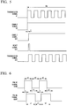
- FIG. 6 is a drawing for explaining how the pulse width of the signal changes when the signal is input to the insulation circuit.
- the rise delay time of the insulation circuit is T
- the fall delay time of the insulation circuit is 2T.
- the pulse signal S100 shown in FIG. 6 may change to the pulse signal S200 shown in FIG. 6 .
- the pulse signal S100 which has a length 4T in the "H” level period, a length 4T in the “L” level period, and a length 4T in the “H” level period may change to the pulse signal S200 which has a length 5T in the "H” level period, a length 3T in the "L” level period, and a length of 5T in the "H” level period.
- the example shown in FIG. 6 is an extreme example for explaining how the pulse width of the signal changes.
- a photocoupler which is sufficiently faster than a transmission rate may be used in order to prevent the change in the pulse width.
- the high speed photocoupler is expensive, a cost of the signal transmission circuit rises.
- the high-speed photocoupler has low withstand voltage in many cases, it is difficult to design the circuit.
- a signal transmission circuit may include a first photocoupler to which a transmission signal is input, an edge detection circuit which is disposed in a primary side of the first photocoupler, the edge detection circuit being configured to detect a rising edge and a falling edge of the transmission signal, and an edge demodulation circuit which is disposed in a secondary side of the first photocoupler, the demodulation circuit being configured to demodulate the transmission signal by using only one of the rising edge and the falling edge of an edge detection signal output from the edge detection circuit via the first photocoupler.
- An aspect of the present invention is to provide a signal transmission circuit, a field device, and a plant control system which can prevent a change in a pulse width of a signal transmitted through an insulation circuit without increasing costs.
- FIG. 1 is a block diagram illustrating a main configuration of a field device including a signal transmission circuit in the embodiment of the present invention.
- a plant control system includes a field device 1 and a controller CNT.
- the field device 1 includes a calculation circuit 10 and a signal transmission circuit 20.
- the field device 1 is installed in a plant or a factory (hereinafter, called simply "plant” as a generic name of them), and the field device 1 transmits a bus signal SB which is a digital signal to a controller CNT through a field bus FB.
- the controller CNT performs various process controls based on the bus signal SB transmitted from the field device 1 through the field bus FB.
- the controller CNT controls an opening of a valve (not shown) installed in the plant based on the bus signal SB transmitted from the field device 1.
- the field bus FB is a wired communication bus installed in the plant.
- the calculation circuit 10 calculates a process value indicating a flow rate (state quantity) of fluid which is a measurement target based on a signal output from a flow rate sensor (not shown) disposed in the field device 1.
- the calculation circuit 10 outputs a transmission signal S1 (a digital signal which is to be transmitted) indicating the process value to the signal transmission circuit 20. Further, the calculation circuit 10 supplies, to the signal transmission circuit 20, an enable signal S2 for controlling an output of the digital signal (the bus signal SB transmitted to the controller CNT through the field bus FB) which is to be output from the field device 1.
- the enable signal S2 is synchronized with the transmission signal S1. As shown in FIG.
- the enable signal S2 is the "H” level in a period (in a communication frame FM) in which the transmission signal S1 is output, and the enable signal S2 is the “L” level in a period (outside the communication frame FM) in which the transmission signal S1 is not output.
- the calculation circuit 10 is realized by a CPU (Central Processing Unit).
- the signal transmission circuit 20 may be configured so that the enable signal S2 is the “L” level in a period in which the transmission signal S1 is output, and the enable signal S2 is the "H” level in a period in which the transmission signal S1 is not output.
- the signal transmission circuit 20 includes an edge detection circuit 21, a light emitting circuit 22a (first light emitting circuit), a light emitting circuit 22b (second light emitting circuit), a photocoupler 23a (first photocoupler), a photocoupler 23b (second photocoupler), a light receiving circuit 24a (first light receiving circuit), a light receiving circuit 24b (second light receiving circuit), an edge demodulation circuit 25, an output control circuit 26, and an initial value setting circuit 27.
- the signal transmission circuit 20 is configured to satisfy an intrinsically safe explosion-proof standard, and the signal transmission circuit 20 transmits the bus signal SB based on the transmission signal S1 and the enable signal S2 output from the calculation circuit 10.
- the edge detection circuit 21 detects a rising edge and a falling edge of the transmission signal S1 output from the calculation circuit 10, and the edge detection circuit 21 outputs an edge detection signal S11 indicating a detection result thereof to the light emitting circuit 22a.
- the edge detection circuit 21 is disposed in a primary side of the photocoupler 23a. In other words, among a light emitting element (light emitting diode) (not shown) and a light receiving element (phototransistor or photodiode) (not shown) disposed in the photocoupler 23a, the edge detection circuit 21 is disposed on a side where the light emitting element is disposed.
- FIG 2 is a block diagram illustrating a configuration example of an edge detection circuit disposed in the signal transmission circuit in the embodiment of the present invention.
- the edge detection circuit 21 includes a delay circuit 31 and an exclusive OR circuit (EXOR circuit) 32 (calculation circuit).
- the delay circuit 31 delays the transmission signal S1 output from the calculation circuit 10 by a predetermined time (for example, about one tenth of the pulse width of the transmission signal S1).
- the exclusive OR circuit 32 calculates an exclusive OR of the transmission signal S1 output from the calculation circuit 10 and the signal output from the delay circuit 31, and the exclusive OR circuit 32 outputs the calculation result as an edge detection signal S11 to the light emitting circuit 22a.
- the light emitting circuit 22a is disposed between the edge detection circuit 21 and the photocoupler 23a, and the light emitting circuit 22a makes the light emitting element (not shown) disposed in the photocoupler 23a emit light based on the edge detection signal S11 output from the edge detection circuit 21.
- the light emitting circuit 22a is a circuit including a resistance or the like for adjusting a current flowing through the light emitting element in order to make the light emitting element (not shown) disposed in the photocoupler 23a emit light properly.
- the photocoupler 23a includes the light emitting element (not shown) and the light receiving element (not shown).
- the photocoupler 23a is an insulation circuit which electrically insulates a primary side (a side where the light emitting element is disposed) and a secondary side (a side where the light receiving element is disposed).
- the light receiving circuit 24a is disposed in the secondary side of the photocoupler 23a.
- the light receiving circuit 24a processes the output signal (light receiving signal) output from the photocoupler 23a, and the light receiving circuit 24a outputs the edge detection signal S12 to the edge demodulation circuit 25.
- the light receiving circuit 24a includes a resistance and a logic circuit, and performs a process such as a waveform shaping of the output signal from the photocoupler 23a.
- the edge demodulation circuit 25 is disposed between the light receiving circuit 24a and the output control circuit 26.
- the edge demodulation circuit 25 demodulates the transmission signal S1, which is a signal to be transmitted, based on the edge detection signal S12 output from the light receiving circuit 24a.
- the edge demodulation circuit 25 outputs the demodulated signal to the output control circuit 26 as the transmission signal S13.
- the edge demodulation circuit 25 demodulates by using only one of the rising edge and the falling edge of the edge detection signal S12 output from the light receiving circuit 24a, and the edge demodulation circuit 25 outputs the demodulated signal as a transmission signal S 13 to the output control circuit 26.
- the edge demodulation circuit 25 demodulates by using the rising edge and outputs the demodulated signal as the transmission signal S13 to the output control circuit 26 will be explained.
- the edge demodulation circuit 25 can be realized by a D flip-flop of edge-trigger type with reset.
- the transmission signal S13 in which the logic is inverted may be output as the demodulated signal.
- resetting (initial value setting) of the edge demodulating circuit 25 is performed by using a reset signal S22 (details will be described later) output from the initial value setting circuit 27.
- the output control circuit 26 is connected to the field bus FB.
- the output control circuit 26 controls an output of the bus signal SB based on an enable signal S21 (details will be described later) output from the light receiving circuit 24b. Specifically, the output control circuit 26 outputs the bus signal SB based on the transmission signal S13 when the enable signal S21 is the "H” level, and the output control circuit 26 does not output the bus signal SB when the enable signal S21 is the "L” level.
- the output control circuit 26 performs the control in order to prevent an erroneous transmission of the bus signal SB due to a bad influence of noise generated outside the communication frame.
- the light emitting circuit 22b is the same circuit as the light emitting circuit 22a, and the light emitting circuit 22b is disposed in the primary side of the photocoupler 23b.
- the light emitting circuit 22b makes a light emitting element (not shown) disposed in the photocoupler 23b emit light based on the enable signal S2 output from the calculation circuit 10.
- the photocoupler 23b includes a light emitting element (light emitting diode) (not shown) and a light receiving element (phototransistor or photodiode) (not shown).
- the photocoupler 23b is an insulation circuit which electrically insulates the primary side (a side where the light emitting element is disposed) and the secondary side (a side where the light receiving element is disposed).
- the light receiving circuit 24b is the same circuit as the light receiving circuit 24a, and the light receiving circuit 24b is disposed in the secondary side of the photocoupler 23b.
- the light receiving circuit 24b processes the output signal output from the photocoupler 23b, and the light receiving circuit 24b outputs an enable signal S21 to the output control circuit 26 and the initial value setting circuit 27.
- the initial value setting circuit 27 outputs a reset signal S22 for resetting the edge demodulation circuit 25 to the edge demodulation circuit 25 based on the enable signal S21 output from the light receiving circuit 24b.
- the reset signal S22 is synchronized with the enable signal S21, the reset signal S22 becomes the "H” level for a predetermined period at a time of rising of the enable signal S21, and the reset signal S22 becomes the "L" level in the other periods.
- the field device 1 is divided into regions R1 and R2 which are electrically insulated by the photocouplers 23a and 23b.
- the region R1 is a region in which a voltage of the commercial power source is permitted to be used.
- the calculation circuit 10 the edge detection circuit 21, and the light emitting circuits 22a and 22b of the signal transmission circuit 20 are arranged.
- the region R2 is a region in which an allowable voltage is limited to be lower than or equal to a voltage defined by the intrinsically safe explosion-proof standard.
- the light receiving circuits 24a and 24b, the edge demodulating circuit 25, the output control circuit 26, and the initial value setting circuit 27 of the signal transmission circuit 20 are arranged.
- FIGS. 3 to 5 are drawings illustrating an example of a signal waveform in the signal transmission circuit in the embodiment of the present invention.
- the calculation circuit 10 disposed in the field device 1 calculates a process value indicating the flow rate of the fluid which is a measurement target at a constant time interval.
- the calculation circuit 10 outputs the transmission signal S1 indicating the process value and the enable signal S2 at a constant interval (transmission interval of the communication frame FM).
- the transmission signal S1 output from the calculation circuit 10 is input to the edge detection circuit 21 of the signal transmission circuit 20.
- the edge detection circuit 21 detects a rising edge and a falling edge of the transmission signal S1 input from the calculation circuit 10. As a result, as shown in FIG. 4 , the edge detection circuit 21 outputs, to the light emitting circuit 22a, the edge detection signal S 11 which becomes the "H" level at a time of the rising edge and the falling edge of the transmission signal S1.
- the transmission signal S1 output from the calculation circuit 10 is a pulse signal which has a length 4T in the "H" level period, a length 4T in the "L” level period, and a length 4T in the "H” level period.
- the edge detection signal S11 output from the edge detection circuit 21 is a pulse signal which becomes "H" level for a predetermined period every time 4T.
- the light emitting element (not shown) disposed in the photocoupler 23a emits light in accordance with the edge detection signal S11.
- the light emitted from the light emitting element (not shown) disposed in the photocoupler 23a is received by the light receiving element (not shown) disposed in the photocoupler 23a, and the photocoupler 23a outputs a light reception signal.
- the light reception signal output from the photocoupler 23a is input to the light receiving circuit 24a.
- the light receiving circuit 24a processes the light reception signal input from the photocoupler 23a, and the light receiving circuit 24a outputs the edge detection signal S12 shown in FIG. 4 to the edge demodulation circuit 25.
- the rise delay time of the photocoupler 23a which is an insulation circuit is T
- the fall delay time of the photocoupler 23a is 2T
- the rise delay time of the photocoupler 23b is T
- the fall delay time of the photocoupler 23b is 2T.
- the timing of the rising edge of the edge detection signal S12 is delayed by the time T in comparison with the timing of the rising edge of the edge detection signal S11, and the timing of the falling edge of the edge detection signal S12 is delayed by the time 2T in comparison with the timing of the falling edge of the edge detection signal S11.
- the enable signal S2 output from the calculation circuit 10 is input to the light emitting circuit 22b of the signal transmission circuit 20, and the light emitting element (not shown) disposed in the photocoupler 23b emits light in accordance with the enable signal S2.
- the light emitted from the light emitting element (not shown) disposed in the photocoupler 23b is received by the light receiving element (not shown) disposed in the photocoupler 23b, and the photocoupler 23b outputs a light reception signal.
- the light reception signal output from the photocoupler 23b is input to the light receiving circuit 24b.
- the light receiving circuit 24b processes the light reception signal input from the photocoupler 23b, and the light receiving circuit 24b outputs the enable signal S21 to the output control circuit 26 and the initial value setting circuit 27 as shown in FIG. 3 .
- FIG. 5 is a magnified view of a part of FIG. 3 (a beginning part of the communication frame FM).
- the initial value setting circuit 27 When the enable signal S21 is input to the initial value setting circuit 27, the initial value setting circuit 27 outputs the reset signal S22 shown in FIG. 3 and FIG. 5 to the edge demodulation circuit 25.
- the reset signal S22 is synchronized with the enable signal S21, the reset signal S22 becomes the "H” level for a predetermined period at a time of rising of the enable signal S21, and the reset signal S22 becomes the "L” level in the other periods.
- the edge demodulation circuit 25 When the reset signal S22 is input to the edge demodulation circuit 25, the edge demodulation circuit 25 is reset based on the reset signal S22.
- the edge detection signal S12 output from the light receiving circuit 24a is also input to the edge demodulation circuit 25.
- the edge demodulation circuit 25 demodulates by using only the rising edge of the edge detection signal S12 output from the light receiving circuit 24a, and the edge demodulation circuit 25 outputs the demodulated signal as the transmission signal S13 to the output control circuit 26. That is, the transmission signal S13 is a signal of which signal level changes every rising edge of the edge detection signal S12. As a result, as shown in FIG.
- the demodulated transmission signal S13 becomes a pulse signal which has a length 4T in the "H” level period, a length 4T in the "L” level period, and a length 4T in the "H” level period. That is, the transmission signal S 13 becomes the same pulse signal as the transmission signal S1.
- the transmission signal S13 demodulated by the edge demodulation circuit 25 is input to the output control circuit 26. If the enable signal S21 output from the light receiving circuit 24b is the "H” level, the output control circuit 26 outputs the transmission signal S 13 as the bus signal SB.
- the bus signal SB output from the output control circuit 26 is transmitted to the controller CNT through the fieldbus FB. If the enable signal S21 output from the light receiving circuit 24b is the "L" level, the output control circuit 26 does not output the bus signal SB.
- the edge detection circuit 21 is disposed in the primary side of the photocoupler 23a, and detects the rising edge and the falling edge of the transmission signal S1.
- the edge demodulation circuit 25 is disposed in the secondary side of the photocoupler 23a, and demodulates by using only one of the rising edge and the falling edge of the edge detection signal S12 output from the edge detection circuit 21 via the photocoupler 23a to generate the transmission signal S13.
- FIG. 7 is a drawing illustrating detail configurations of the edge demodulation circuit and the initial value setting circuit.
- the initial value setting circuit 27 includes a NOT circuit 271, a delay circuit 272, and an AND circuit 273.
- the enable signal S21 is input from the light receiving circuit 24b to the initial value setting circuit 27, the NOT circuit 271 inverts "L” level and "H” level of the enable signal S21.
- the delay circuit 272 delays the signal input from the NOT circuit 271. If both the enable signal S21 output from the light receiving circuit 24b and the signal output from the delay circuit 272 are "H" level, the AND circuit 273 outputs the reset signal S22 which is "H" level to the edge demodulation circuit 25.
- the edge demodulation circuit 25 includes a NOT circuit 251 and a D-flip-flop 252.
- the NOT circuit 251 inverts "L" level and "H” level of the reset signal S22 output from the initial value setting circuit 27.
- the signal output from the NOT circuit 251 is input to the PR-bar terminal of the D-flip-flop 252.
- the level of the transmission signal S13 output from the Q terminal is reset based on the signal input to the PR-bar terminal.
- the enable signal S21 output from the light receiving circuit 24b is input to the CLR-bar terminal.
- the D terminal and the Q-bar terminal are connected to each other.
- the transmission signal S 13 output from the Q terminal is "H" level
- the signal input to the D terminal is "L” level.
- the edge detection signal S12 is input from the light receiving circuit 24a to the CLK terminal.
- the level of the transmission signal S13 output from the Q terminal is changed every time a rising edge of the edge detection signal S12 is input to the CLK terminal. For this reason, for example, when a first rising edge of the edge detection signal S12 is input to the CLK terminal, the transmission signal S13 becomes "H” level, and when a second rising edge of the edge detection signal S12 is input to the CLK terminal, the transmission signal S 13 becomes “L” level. In this way, the level of the transmission signal S13 output from the Q terminal is changed every time a rising edge of the edge detection signal S12 is input to the CLK terminal.
- the D-flip-flop 252 is disposed in the edge demodulation circuit 25 so that the edge detection signal can be demodulated by simple configuration.
- FIG. 7 is an example, and the edge demodulation circuit 25 and the initial value setting circuit 27 are not limited to the configuration shown in FIG. 7 .
- the signal transmission circuit 20 described in the above-described embodiment transmits the digital signal to the external controller CNT through the fieldbus FB, but it is not limited thereto.
- the signal transmission circuit 20 may receive a digital signal transmitted from the external controller CNT through the fieldbus FB.
- the signal transmission circuit 20 may transmit a digital signal to the external controller CNT and receive a digital signal from the external controller CNT through the fieldbus FB. That is, the signal transmission circuit 20 may be anything as long as it can transmit a signal via the photocoupler.
- the signal transmission circuit 20 becomes possible to receive a digital signal transmitted through the fieldbus FB.
- the digital signal transmitted through the fieldbus FB is received by the reception circuit, and a signal corresponding to the transmission signal S1 shown in FIG. 1 is output from the reception circuit.
- the signal output from the receiving circuit is demodulated by the circuit including the edge detecting circuit 21, the light emitting circuit 22a, the photocoupler 23a, the light receiving circuit 24a, and the edge demodulating circuit 25, and the signal is output as a signal corresponding to the transmission signal S13 shown in FIG. 1 .
- the signal is transmitted through the external fieldbus FB connected to the field device 1, but not limited thereto.
- the present invention can also be used for transmitting and receiving signals used inside the device (for example, inside the field device 1).
- the field device 1 is a flowmeter, but it is not limited thereto.
- the field device 1 may be a sensor device such as a temperature sensor, a valve device such as a flow rate control valve and an open/close valve, an actuator device such as a fan and a motor, an imaging device such as a camera and a video camera for photographing situations and objects in the plant, an audio device such as a microphone for collecting abnormal sound and a speaker for emitting a warning sound, a position detecting device for outputting position information of each device, or other devices.
- the signal transmission circuit 20 described in the above-described embodiment transmits a digital signal to the controller CNT through the fieldbus FB which is a wired communication bus installed in a field of the plant, but not limited thereto.
- the signal transmission circuit 20 may perform a wireless communication in conformity with industrial wireless communication standards such as ISA100.11a and WirelessHART (registered trademark) to communicate with the controller CNT.
- the plant includes a petroleum refining plant, a gas producing/supplying plant, a production plant of chemistry or medicine, a plant controlling to mine a wellhead (for example, a gas field and an oil field) and controlling a transporting pipeline thereof, a power-generating plant (for example, hydro power, thermal power, nuclear power, solar power, and wind power), a monitoring control plant of water supply and sewerage, and so on.
- a petroleum refining plant for example, a gas field and an oil field
- a plant controlling to mine a wellhead for example, a gas field and an oil field
- a power-generating plant for example, hydro power, thermal power, nuclear power, solar power, and wind power
- a monitoring control plant of water supply and sewerage and so on.
- the term "configured” is used to describe a component, unit or part of a device includes hardware and/or software that is constructed and/or programmed to carry out the desired function.
- unit is used to describe a component, unit or part of a hardware and/or software that is constructed and/or programmed to carry out the desired function.
- Typical examples of the hardware may include, but are not limited to, a device and a circuit.
Landscapes
- Engineering & Computer Science (AREA)
- Physics & Mathematics (AREA)
- General Engineering & Computer Science (AREA)
- Computer Hardware Design (AREA)
- Signal Processing (AREA)
- Mathematical Physics (AREA)
- Computer Networks & Wireless Communication (AREA)
- Computing Systems (AREA)
- Manufacturing & Machinery (AREA)
- Quality & Reliability (AREA)
- General Physics & Mathematics (AREA)
- Automation & Control Theory (AREA)
- Nonlinear Science (AREA)
- Power Engineering (AREA)
- Electromagnetism (AREA)
- Arrangements For Transmission Of Measured Signals (AREA)
- Photo Coupler, Interrupter, Optical-To-Optical Conversion Devices (AREA)
Abstract
Description
- The disclosure relates to a signal transmission circuit, a field device, and a plant control system.
- Priority is claimed on
Japanese Patent Application No. 2016-155425, filed August 8, 2016 - In a plant and a factory, a process control system is constructed, and an advanced automatic operation is implemented. In the process control system, field devices (measurement devices and manipulation devices) and a control device which controls the field devices are connected to each other. In the process control system, the field device and the control device are connected by an analog transmission line for transmitting an analog signal such as a signal of "4 to 20 [mA]", or connected by a communication bus for transmitting a digital signal called as a fieldbus.
- The field devices are often configured to satisfy an intrinsically safe explosion-proof standard because the field devices may be installed in a dangerous place, such as a place where flammable gases are used. For example, in the field device connected to the fieldbus, an insulation circuit such as a photocoupler and a transformer is disposed in a signal transmission circuit for transmitting a signal. The insulation circuit electrically insulates a circuit (for example, a calculation circuit for calculating a process amount) disposed inside the field device from the outside (for example, a transmission line and a communication bus).
- An example of a conventional signal transmission circuit which transmits a pulse signal via an insulation circuit is disclosed in
Japanese Unexamined Patent Application Publication No. 2013-222978 Japanese Unexamined Patent Application Publication No. 2011-124331 WO 2010/061511 . For example,Japanese Unexamined Patent Publication No. 2013-222978 Japanese Unexamined Patent Publication No. 2011-124331 WO 2010/061511 disclose a signal propagation circuit or a signal transmission device including a photocoupler. - Meanwhile, in the photocoupler, a propagation delay time (hereinafter, called as "rise delay time") of a rising signal and a propagation delay time (hereinafter, called as "fall delay time") of a falling signal may be different from each other. The rising signal is a signal changing from "L (low)" level to "H (high)" level, and the falling signal is a signal changing from "H" level to "L" level. Similarly, in a light emitting circuit which makes the photocoupler emit light and a light receiving circuit which processes an output signal from the photocoupler, the rise delay time and the fall delay time may be different from each other. In a case that the photocoupler is used as an insulation circuit (furthermore, in a case that the light emitting circuit and the light receiving circuit are used as a peripheral circuit of an insulation circuit), a pulse width of the signal may change.
-
FIG. 6 is a drawing for explaining how the pulse width of the signal changes when the signal is input to the insulation circuit. InFIG. 6 , for example, the rise delay time of the insulation circuit is T, and the fall delay time of the insulation circuit is 2T. When the pulse signal S100 shown inFIG. 6 is input to the insulation circuit, the pulse signal S100 may change to the pulse signal S200 shown inFIG. 6 . Specifically, the pulse signal S100 which has alength 4T in the "H" level period, alength 4T in the "L" level period, and alength 4T in the "H" level period may change to the pulse signal S200 which has alength 5T in the "H" level period, alength 3T in the "L" level period, and a length of 5T in the "H" level period. The example shown inFIG. 6 is an extreme example for explaining how the pulse width of the signal changes. - It is considered that a photocoupler which is sufficiently faster than a transmission rate may be used in order to prevent the change in the pulse width. However, since the high speed photocoupler is expensive, a cost of the signal transmission circuit rises. Furthermore, since the high-speed photocoupler has low withstand voltage in many cases, it is difficult to design the circuit.
- A signal transmission circuit may include a first photocoupler to which a transmission signal is input, an edge detection circuit which is disposed in a primary side of the first photocoupler, the edge detection circuit being configured to detect a rising edge and a falling edge of the transmission signal, and an edge demodulation circuit which is disposed in a secondary side of the first photocoupler, the demodulation circuit being configured to demodulate the transmission signal by using only one of the rising edge and the falling edge of an edge detection signal output from the edge detection circuit via the first photocoupler.
- Further features and aspects of the present disclosure will become apparent from the following detailed description of exemplary embodiments with reference to the attached drawings.
-
-
FIG. 1 is a block diagram illustrating a main configuration of a field device including a signal transmission circuit in the embodiment of the present invention. -
FIG. 2 is a block diagram illustrating a configuration example of an edge detection circuit disposed in the signal transmission circuit in the embodiment of the present invention. -
FIG. 3 is a drawing illustrating an example of a signal waveform in the signal transmission circuit in the embodiment of the present invention. -
FIG. 4 is a drawing illustrating an example of a signal waveform in the signal transmission circuit in the embodiment of the present invention. -
FIG. 5 is a drawing illustrating an example of a signal waveform in the signal transmission circuit in the embodiment of the present invention. -
FIG. 6 is a drawing for explaining how the pulse width of the signal changes when the signal is input to the insulation circuit. -
FIG. 7 is a drawing illustrating detail configurations of the edge demodulation circuit and the initial value setting circuit. - The embodiments of the present invention will be now described herein with reference to illustrative preferred embodiments. Those skilled in the art will recognize that many alternative preferred embodiments can be accomplished using the teaching of the present invention and that the present invention is not limited to the preferred embodiments illustrated herein for explanatory purposes.
- An aspect of the present invention is to provide a signal transmission circuit, a field device, and a plant control system which can prevent a change in a pulse width of a signal transmitted through an insulation circuit without increasing costs.
- Hereinafter, a signal transmission circuit in an embodiment of the present invention will be described in detail with reference to drawings.
FIG. 1 is a block diagram illustrating a main configuration of a field device including a signal transmission circuit in the embodiment of the present invention. As shown inFIG. 1 , a plant control system includes afield device 1 and a controller CNT. Thefield device 1 includes acalculation circuit 10 and asignal transmission circuit 20. Thefield device 1 is installed in a plant or a factory (hereinafter, called simply "plant" as a generic name of them), and thefield device 1 transmits a bus signal SB which is a digital signal to a controller CNT through a field bus FB. - In the present embodiment, in order to be understood easily, an example where the
field device 1 is a flow meter will be explained. The controller CNT performs various process controls based on the bus signal SB transmitted from thefield device 1 through the field bus FB. For example, the controller CNT controls an opening of a valve (not shown) installed in the plant based on the bus signal SB transmitted from thefield device 1. For example, the field bus FB is a wired communication bus installed in the plant. - The
calculation circuit 10 calculates a process value indicating a flow rate (state quantity) of fluid which is a measurement target based on a signal output from a flow rate sensor (not shown) disposed in thefield device 1. Thecalculation circuit 10 outputs a transmission signal S1 (a digital signal which is to be transmitted) indicating the process value to thesignal transmission circuit 20. Further, thecalculation circuit 10 supplies, to thesignal transmission circuit 20, an enable signal S2 for controlling an output of the digital signal (the bus signal SB transmitted to the controller CNT through the field bus FB) which is to be output from thefield device 1. The enable signal S2 is synchronized with the transmission signal S1. As shown inFIG. 3 , the enable signal S2 is the "H" level in a period (in a communication frame FM) in which the transmission signal S1 is output, and the enable signal S2 is the "L" level in a period (outside the communication frame FM) in which the transmission signal S1 is not output. For example, thecalculation circuit 10 is realized by a CPU (Central Processing Unit). Thesignal transmission circuit 20 may be configured so that the enable signal S2 is the "L" level in a period in which the transmission signal S1 is output, and the enable signal S2 is the "H" level in a period in which the transmission signal S1 is not output. - The
signal transmission circuit 20 includes anedge detection circuit 21, alight emitting circuit 22a (first light emitting circuit), alight emitting circuit 22b (second light emitting circuit), aphotocoupler 23a (first photocoupler), a photocoupler 23b (second photocoupler), alight receiving circuit 24a (first light receiving circuit), alight receiving circuit 24b (second light receiving circuit), anedge demodulation circuit 25, anoutput control circuit 26, and an initialvalue setting circuit 27. Thesignal transmission circuit 20 is configured to satisfy an intrinsically safe explosion-proof standard, and thesignal transmission circuit 20 transmits the bus signal SB based on the transmission signal S1 and the enable signal S2 output from thecalculation circuit 10. - The
edge detection circuit 21 detects a rising edge and a falling edge of the transmission signal S1 output from thecalculation circuit 10, and theedge detection circuit 21 outputs an edge detection signal S11 indicating a detection result thereof to thelight emitting circuit 22a. Theedge detection circuit 21 is disposed in a primary side of thephotocoupler 23a. In other words, among a light emitting element (light emitting diode) (not shown) and a light receiving element (phototransistor or photodiode) (not shown) disposed in thephotocoupler 23a, theedge detection circuit 21 is disposed on a side where the light emitting element is disposed. -
FIG 2 is a block diagram illustrating a configuration example of an edge detection circuit disposed in the signal transmission circuit in the embodiment of the present invention. As shown inFIG. 2 , theedge detection circuit 21 includes adelay circuit 31 and an exclusive OR circuit (EXOR circuit) 32 (calculation circuit). Thedelay circuit 31 delays the transmission signal S1 output from thecalculation circuit 10 by a predetermined time (for example, about one tenth of the pulse width of the transmission signal S1). The exclusive ORcircuit 32 calculates an exclusive OR of the transmission signal S1 output from thecalculation circuit 10 and the signal output from thedelay circuit 31, and theexclusive OR circuit 32 outputs the calculation result as an edge detection signal S11 to thelight emitting circuit 22a. - The
light emitting circuit 22a is disposed between theedge detection circuit 21 and thephotocoupler 23a, and thelight emitting circuit 22a makes the light emitting element (not shown) disposed in thephotocoupler 23a emit light based on the edge detection signal S11 output from theedge detection circuit 21. Thelight emitting circuit 22a is a circuit including a resistance or the like for adjusting a current flowing through the light emitting element in order to make the light emitting element (not shown) disposed in thephotocoupler 23a emit light properly. - The
photocoupler 23a includes the light emitting element (not shown) and the light receiving element (not shown). Thephotocoupler 23a is an insulation circuit which electrically insulates a primary side (a side where the light emitting element is disposed) and a secondary side (a side where the light receiving element is disposed). Thelight receiving circuit 24a is disposed in the secondary side of thephotocoupler 23a. Thelight receiving circuit 24a processes the output signal (light receiving signal) output from thephotocoupler 23a, and thelight receiving circuit 24a outputs the edge detection signal S12 to theedge demodulation circuit 25. For example, thelight receiving circuit 24a includes a resistance and a logic circuit, and performs a process such as a waveform shaping of the output signal from thephotocoupler 23a. - The
edge demodulation circuit 25 is disposed between thelight receiving circuit 24a and theoutput control circuit 26. Theedge demodulation circuit 25 demodulates the transmission signal S1, which is a signal to be transmitted, based on the edge detection signal S12 output from thelight receiving circuit 24a. Theedge demodulation circuit 25 outputs the demodulated signal to theoutput control circuit 26 as the transmission signal S13. Specifically, theedge demodulation circuit 25 demodulates by using only one of the rising edge and the falling edge of the edge detection signal S12 output from thelight receiving circuit 24a, and theedge demodulation circuit 25 outputs the demodulated signal as atransmission signal S 13 to theoutput control circuit 26. In the present embodiment, an example where theedge demodulation circuit 25 demodulates by using the rising edge and outputs the demodulated signal as the transmission signal S13 to theoutput control circuit 26 will be explained. - For example, the
edge demodulation circuit 25 can be realized by a D flip-flop of edge-trigger type with reset. In a case of using theedge demodulation circuit 25, if a timing of resetting is inappropriate, the transmission signal S13 in which the logic is inverted may be output as the demodulated signal. In order to avoid this, in the present embodiment, resetting (initial value setting) of theedge demodulating circuit 25 is performed by using a reset signal S22 (details will be described later) output from the initialvalue setting circuit 27. - The
output control circuit 26 is connected to the field bus FB. Theoutput control circuit 26 controls an output of the bus signal SB based on an enable signal S21 (details will be described later) output from thelight receiving circuit 24b. Specifically, theoutput control circuit 26 outputs the bus signal SB based on the transmission signal S13 when the enable signal S21 is the "H" level, and theoutput control circuit 26 does not output the bus signal SB when the enable signal S21 is the "L" level. Theoutput control circuit 26 performs the control in order to prevent an erroneous transmission of the bus signal SB due to a bad influence of noise generated outside the communication frame. - The
light emitting circuit 22b is the same circuit as thelight emitting circuit 22a, and thelight emitting circuit 22b is disposed in the primary side of the photocoupler 23b. Thelight emitting circuit 22b makes a light emitting element (not shown) disposed in the photocoupler 23b emit light based on the enable signal S2 output from thecalculation circuit 10. Similar to thephotocoupler 23a, the photocoupler 23b includes a light emitting element (light emitting diode) (not shown) and a light receiving element (phototransistor or photodiode) (not shown). The photocoupler 23b is an insulation circuit which electrically insulates the primary side (a side where the light emitting element is disposed) and the secondary side (a side where the light receiving element is disposed). Thelight receiving circuit 24b is the same circuit as thelight receiving circuit 24a, and thelight receiving circuit 24b is disposed in the secondary side of the photocoupler 23b. Thelight receiving circuit 24b processes the output signal output from the photocoupler 23b, and thelight receiving circuit 24b outputs an enable signal S21 to theoutput control circuit 26 and the initialvalue setting circuit 27. - The initial
value setting circuit 27 outputs a reset signal S22 for resetting theedge demodulation circuit 25 to theedge demodulation circuit 25 based on the enable signal S21 output from thelight receiving circuit 24b. Specifically, the reset signal S22 is synchronized with the enable signal S21, the reset signal S22 becomes the "H" level for a predetermined period at a time of rising of the enable signal S21, and the reset signal S22 becomes the "L" level in the other periods. - As shown in
FIG. 1 , thefield device 1 is divided into regions R1 and R2 which are electrically insulated by thephotocouplers 23a and 23b. For example, the region R1 is a region in which a voltage of the commercial power source is permitted to be used. In the region R1, thecalculation circuit 10, theedge detection circuit 21, and thelight emitting circuits signal transmission circuit 20 are arranged. On the other hand, for example, the region R2 is a region in which an allowable voltage is limited to be lower than or equal to a voltage defined by the intrinsically safe explosion-proof standard. In the region R2, thelight receiving circuits edge demodulating circuit 25, theoutput control circuit 26, and the initialvalue setting circuit 27 of thesignal transmission circuit 20 are arranged. - Next, an operation of the
field device 1 in the above configuration will be described.FIGS. 3 to 5 are drawings illustrating an example of a signal waveform in the signal transmission circuit in the embodiment of the present invention. In the following description, in order to be understood easily, an example of measuring a flow rate of the fluid which is a measurement target at a predetermined time interval in thefield device 1 will be explained. For this reason, thecalculation circuit 10 disposed in thefield device 1 calculates a process value indicating the flow rate of the fluid which is a measurement target at a constant time interval. As a result, as shown inFIG. 3 , thecalculation circuit 10 outputs the transmission signal S1 indicating the process value and the enable signal S2 at a constant interval (transmission interval of the communication frame FM). - The transmission signal S1 output from the
calculation circuit 10 is input to theedge detection circuit 21 of thesignal transmission circuit 20. Theedge detection circuit 21 detects a rising edge and a falling edge of the transmission signal S1 input from thecalculation circuit 10. As a result, as shown inFIG. 4 , theedge detection circuit 21 outputs, to thelight emitting circuit 22a, the edgedetection signal S 11 which becomes the "H" level at a time of the rising edge and the falling edge of the transmission signal S1. Here, as shown inFIG. 4 , the transmission signal S1 output from thecalculation circuit 10 is a pulse signal which has alength 4T in the "H" level period, alength 4T in the "L" level period, and alength 4T in the "H" level period. In this case, as shown inFIG. 4 , the edge detection signal S11 output from theedge detection circuit 21 is a pulse signal which becomes "H" level for a predetermined period everytime 4T. - When the edge detection signal S11 output from the
edge detection circuit 21 is input to thelight emitting circuit 22a, the light emitting element (not shown) disposed in thephotocoupler 23a emits light in accordance with the edge detection signal S11. The light emitted from the light emitting element (not shown) disposed in thephotocoupler 23a is received by the light receiving element (not shown) disposed in thephotocoupler 23a, and thephotocoupler 23a outputs a light reception signal. The light reception signal output from thephotocoupler 23a is input to thelight receiving circuit 24a. Thelight receiving circuit 24a processes the light reception signal input from thephotocoupler 23a, and thelight receiving circuit 24a outputs the edge detection signal S12 shown inFIG. 4 to theedge demodulation circuit 25. - In the example shown in
FIG. 4 , the rise delay time of thephotocoupler 23a which is an insulation circuit is T, and the fall delay time of thephotocoupler 23a is 2T. Also, the rise delay time of the photocoupler 23b is T, and the fall delay time of the photocoupler 23b is 2T. In order to describe simply, no delay occurs in thelight emitting circuits light receiving circuits FIG. 4 , the timing of the rising edge of the edge detection signal S12 is delayed by the time T in comparison with the timing of the rising edge of the edge detection signal S11, and the timing of the falling edge of the edge detection signal S12 is delayed by thetime 2T in comparison with the timing of the falling edge of the edge detection signal S11. - On the other hand, the enable signal S2 output from the
calculation circuit 10 is input to thelight emitting circuit 22b of thesignal transmission circuit 20, and the light emitting element (not shown) disposed in the photocoupler 23b emits light in accordance with the enable signal S2. The light emitted from the light emitting element (not shown) disposed in the photocoupler 23b is received by the light receiving element (not shown) disposed in the photocoupler 23b, and the photocoupler 23b outputs a light reception signal. The light reception signal output from the photocoupler 23b is input to thelight receiving circuit 24b. Thelight receiving circuit 24b processes the light reception signal input from the photocoupler 23b, and thelight receiving circuit 24b outputs the enable signal S21 to theoutput control circuit 26 and the initialvalue setting circuit 27 as shown inFIG. 3 . - As described above, the rise delay time of the photocoupler 23b is T. Therefore, as shown in
FIG. 5 , the timing of the rising edge of the enable signal S21 is delayed by the time T in comparison with the timing of the rising edge of the enable signal S2.FIG. 5 is a magnified view of a part ofFIG. 3 (a beginning part of the communication frame FM). - When the enable signal S21 is input to the initial
value setting circuit 27, the initialvalue setting circuit 27 outputs the reset signal S22 shown inFIG. 3 andFIG. 5 to theedge demodulation circuit 25. The reset signal S22 is synchronized with the enable signal S21, the reset signal S22 becomes the "H" level for a predetermined period at a time of rising of the enable signal S21, and the reset signal S22 becomes the "L" level in the other periods. When the reset signal S22 is input to theedge demodulation circuit 25, theedge demodulation circuit 25 is reset based on the reset signal S22. - As described above, the edge detection signal S12 output from the
light receiving circuit 24a is also input to theedge demodulation circuit 25. As shown inFIG. 4 , theedge demodulation circuit 25 demodulates by using only the rising edge of the edge detection signal S12 output from thelight receiving circuit 24a, and theedge demodulation circuit 25 outputs the demodulated signal as the transmission signal S13 to theoutput control circuit 26. That is, the transmission signal S13 is a signal of which signal level changes every rising edge of the edge detection signal S12. As a result, as shown inFIG. 4 , the demodulated transmission signal S13 becomes a pulse signal which has alength 4T in the "H" level period, alength 4T in the "L" level period, and alength 4T in the "H" level period. That is, thetransmission signal S 13 becomes the same pulse signal as the transmission signal S1. - The transmission signal S13 demodulated by the
edge demodulation circuit 25 is input to theoutput control circuit 26. If the enable signal S21 output from thelight receiving circuit 24b is the "H" level, theoutput control circuit 26 outputs thetransmission signal S 13 as the bus signal SB. The bus signal SB output from theoutput control circuit 26 is transmitted to the controller CNT through the fieldbus FB. If the enable signal S21 output from thelight receiving circuit 24b is the "L" level, theoutput control circuit 26 does not output the bus signal SB. - As described above, in the present embodiment, the
edge detection circuit 21 is disposed in the primary side of thephotocoupler 23a, and detects the rising edge and the falling edge of the transmission signal S1. Theedge demodulation circuit 25 is disposed in the secondary side of thephotocoupler 23a, and demodulates by using only one of the rising edge and the falling edge of the edge detection signal S12 output from theedge detection circuit 21 via thephotocoupler 23a to generate the transmission signal S13. Thus, it is possible to prevent a change in a pulse width of the signal transmitted via thephotocoupler 23a, which is an insulation circuit, without increasing costs. -
FIG. 7 is a drawing illustrating detail configurations of the edge demodulation circuit and the initial value setting circuit. As shown inFIG. 7 , the initialvalue setting circuit 27 includes aNOT circuit 271, adelay circuit 272, and an ANDcircuit 273. When the enable signal S21 is input from thelight receiving circuit 24b to the initialvalue setting circuit 27, theNOT circuit 271 inverts "L" level and "H" level of the enable signal S21. Thedelay circuit 272 delays the signal input from theNOT circuit 271. If both the enable signal S21 output from thelight receiving circuit 24b and the signal output from thedelay circuit 272 are "H" level, the ANDcircuit 273 outputs the reset signal S22 which is "H" level to theedge demodulation circuit 25. - The
edge demodulation circuit 25 includes aNOT circuit 251 and a D-flip-flop 252. TheNOT circuit 251 inverts "L" level and "H" level of the reset signal S22 output from the initialvalue setting circuit 27. The signal output from theNOT circuit 251 is input to the PR-bar terminal of the D-flip-flop 252. The level of the transmission signal S13 output from the Q terminal is reset based on the signal input to the PR-bar terminal. On the other hand, the enable signal S21 output from thelight receiving circuit 24b is input to the CLR-bar terminal. The D terminal and the Q-bar terminal are connected to each other. For this reason, for example, if thetransmission signal S 13 output from the Q terminal is "H" level, the signal input to the D terminal is "L" level. The edge detection signal S12 is input from thelight receiving circuit 24a to the CLK terminal. The level of the transmission signal S13 output from the Q terminal is changed every time a rising edge of the edge detection signal S12 is input to the CLK terminal. For this reason, for example, when a first rising edge of the edge detection signal S12 is input to the CLK terminal, the transmission signal S13 becomes "H" level, and when a second rising edge of the edge detection signal S12 is input to the CLK terminal, thetransmission signal S 13 becomes "L" level. In this way, the level of the transmission signal S13 output from the Q terminal is changed every time a rising edge of the edge detection signal S12 is input to the CLK terminal. - As described above, the D-flip-
flop 252 is disposed in theedge demodulation circuit 25 so that the edge detection signal can be demodulated by simple configuration. In addition,FIG. 7 is an example, and theedge demodulation circuit 25 and the initialvalue setting circuit 27 are not limited to the configuration shown inFIG. 7 . - Although the signal transmission circuit according to the embodiment of the present invention has been described above, the present invention is not limited to the above-described embodiments, and can be freely modified within the scope of the present invention. For example, the
signal transmission circuit 20 described in the above-described embodiment transmits the digital signal to the external controller CNT through the fieldbus FB, but it is not limited thereto. For example, thesignal transmission circuit 20 may receive a digital signal transmitted from the external controller CNT through the fieldbus FB. In addition, thesignal transmission circuit 20 may transmit a digital signal to the external controller CNT and receive a digital signal from the external controller CNT through the fieldbus FB. That is, thesignal transmission circuit 20 may be anything as long as it can transmit a signal via the photocoupler. - For example, by changing the
signal transmission circuit 20 shown inFIG. 1 in accordance with the following (1) to (3), thesignal transmission circuit 20 becomes possible to receive a digital signal transmitted through the fieldbus FB. - (1) Reversing the input and the output of the
signal transmission circuit 20. - (2) Providing a reception circuit (a circuit for receiving a digital signal transmitted through the fieldbus FB) in a pre-stage of the
edge detection circuit 21. - (3) Omitting the
light emitting circuit 22b, the photocoupler 23b, thelight receiving circuit 24b, theoutput control circuit 26, and the initialvalue setting circuit 27. - In the
signal transmission circuit 20 having such a configuration, the digital signal transmitted through the fieldbus FB is received by the reception circuit, and a signal corresponding to the transmission signal S1 shown inFIG. 1 is output from the reception circuit. The signal output from the receiving circuit is demodulated by the circuit including theedge detecting circuit 21, thelight emitting circuit 22a, thephotocoupler 23a, thelight receiving circuit 24a, and theedge demodulating circuit 25, and the signal is output as a signal corresponding to the transmission signal S13 shown inFIG. 1 . - In the above-described embodiment, the signal is transmitted through the external fieldbus FB connected to the
field device 1, but not limited thereto. For example, the present invention can also be used for transmitting and receiving signals used inside the device (for example, inside the field device 1). - In the embodiment described above, the
field device 1 is a flowmeter, but it is not limited thereto. For example, thefield device 1 may be a sensor device such as a temperature sensor, a valve device such as a flow rate control valve and an open/close valve, an actuator device such as a fan and a motor, an imaging device such as a camera and a video camera for photographing situations and objects in the plant, an audio device such as a microphone for collecting abnormal sound and a speaker for emitting a warning sound, a position detecting device for outputting position information of each device, or other devices. - The
signal transmission circuit 20 described in the above-described embodiment transmits a digital signal to the controller CNT through the fieldbus FB which is a wired communication bus installed in a field of the plant, but not limited thereto. For example, thesignal transmission circuit 20 may perform a wireless communication in conformity with industrial wireless communication standards such as ISA100.11a and WirelessHART (registered trademark) to communicate with the controller CNT. - The plant includes a petroleum refining plant, a gas producing/supplying plant, a production plant of chemistry or medicine, a plant controlling to mine a wellhead (for example, a gas field and an oil field) and controlling a transporting pipeline thereof, a power-generating plant (for example, hydro power, thermal power, nuclear power, solar power, and wind power), a monitoring control plant of water supply and sewerage, and so on.
- As used herein, the following directional terms "front, back, above, downward, right, left, vertical, horizontal, below, transverse, row and column" as well as any other similar directional terms refer to those instructions of a device equipped with the present invention. Accordingly, these terms, as utilized to describe the present invention should be interpreted relative to a device equipped with the present invention.
- The term "configured" is used to describe a component, unit or part of a device includes hardware and/or software that is constructed and/or programmed to carry out the desired function.
- Moreover, terms that are expressed as "means-plus function" in the claims should include any structure that can be utilized to carry out the function of that part of the present invention.
- The term "unit" is used to describe a component, unit or part of a hardware and/or software that is constructed and/or programmed to carry out the desired function. Typical examples of the hardware may include, but are not limited to, a device and a circuit.
- While preferred embodiments of the present invention have been described and illustrated above, it should be understood that these are examples of the present invention and are not to be considered as limiting. Additions, omissions, substitutions, and other modifications can be made without departing from the scope of the present invention. Accordingly, the present invention is not to be considered as being limited by the foregoing description, and is only limited by the scope of the claims.
Claims (15)
- A signal transmission circuit comprising:a first photocoupler to which a transmission signal is input;an edge detection circuit which is disposed in a primary side of the first photocoupler, the edge detection circuit being configured to detect a rising edge and a falling edge of the transmission signal; andan edge demodulation circuit which is disposed in a secondary side of the first photocoupler, the demodulation circuit being configured to demodulate the transmission signal by using only one of the rising edge and the falling edge of an edge detection signal output from the edge detection circuit via the first photocoupler.
- The signal transmission circuit according to claim 1, further comprising:a second photocoupler to which an enable signal is input; andan output control circuit configured to control an output of the signal demodulated by the edge demodulation circuit based on the enable signal transmitted via the second photocoupler.
- The signal transmission circuit according to claim 2, further comprising:an initial value setting circuit configured to set an initial value of the signal demodulated by the edge demodulation circuit based on the enable signal transmitted via the second photocoupler.
- The signal transmission circuit according to claim 3, further comprising:a first light emitting circuit which is disposed in the primary side of the first photocoupler;a second light emitting circuit which is disposed in the primary side of the second photocoupler;a first light receiving circuit which is disposed in the secondary side of the first photocoupler; anda second light receiving circuit which is disposed in the secondary side of the second photocoupler.
- The signal transmission circuit according to any one of claims 1 to 4,
wherein the edge detection circuit comprises:a delay circuit configured to delay the transmission signal by a predetermined time; andan exclusive OR circuit configured to calculate an exclusive OR of the transmission signal and a signal delayed by the delay circuit. - The signal transmission circuit according to claim 4,
wherein the edge detection circuit is configured to generate the edge detection signal based on the rising edge and the falling edge, and configured to output the edge detection signal to the first light emitting circuit. - The signal transmission circuit according to claim 6,
wherein the first light emitting circuit is configured to output, to the first light receiving circuit via the first photocoupler, the edge detection signal output from the edge detection circuit, and
wherein the first light receiving circuit is configured to output, to the edge demodulation circuit, the edge detection signal output from the first light emitting circuit via the first photocoupler. - The signal transmission circuit according to claim 4,
wherein the second light emitting circuit is configured to output the enable signal to the second light receiving circuit via the second photocoupler, and
wherein the second light receiving circuit is configured to output, to the output control circuit and the initial value setting circuit, the enable signal output from the second light emitting circuit via the second photocoupler. - The signal transmission circuit according to claim 8,
wherein the initial value setting circuit is configured to output, to the edge demodulation circuit, a reset signal which is synchronized with the enable signal output from the second light receiving circuit, and
wherein the edge demodulation circuit is configured to be reset based on the reset signal output from the initial value setting circuit. - A field device comprising:a calculation circuit configured to calculate a process value indicating a state quantity of a measurement target; anda signal transmission circuit configured to transmit a transmission signal indicating the process value calculated by the calculation circuit,wherein the signal transmission circuit comprises:a first photocoupler to which the transmission signal is input from the calculation circuit;an edge detection circuit which is disposed in a primary side of the first photocoupler, the edge detection circuit being configured to detect a rising edge and a falling edge of a signal to be transmitted; andan edge demodulation circuit which is disposed in a secondary side of the first photocoupler, the demodulation circuit being configured to demodulate the signal to be transmitted by using only one of the rising edge and the falling edge of an edge detection signal output from the edge detection circuit via the first photocoupler.
- The field device according to claim 10, further comprising:a second photocoupler to which an enable signal is input; andan output control circuit configured to control an output of the signal demodulated by the edge demodulation circuit based on the enable signal transmitted via the second photocoupler.
- The field device according to claim 11, further comprising:an initial value setting circuit configured to set an initial value of the signal demodulated by the edge demodulation circuit based on the enable signal transmitted via the second photocoupler.
- The field device according to claim 12, further comprising:a first light emitting circuit which is disposed in the primary side of the first photocoupler;a second light emitting circuit which is disposed in the primary side of the second photocoupler;a first light receiving circuit which is disposed in the secondary side of the first photocoupler; anda second light receiving circuit which is disposed in the secondary side of the second photocoupler.
- The field device according to any one of claims 10 to 13,
wherein the edge detection circuit comprises:a delay circuit configured to delay the signal to be transmitted by a predetermined time; andan exclusive OR circuit configured to calculate an exclusive OR of the signal to be transmitted and a signal delayed by the delay circuit. - A plant control system comprising:a field device which is installed in a plant; anda controller which is communicably connected to the field device, the controller being configured to control the field device,wherein the field device comprises:a calculation circuit configured to calculate a process value indicating a state quantity of a measurement target; anda signal transmission circuit configured to transmit a transmission signal indicating the process value calculated by the calculation circuit,wherein the signal transmission circuit comprises:a first photocoupler to which the transmission signal is input from the calculation circuit;an edge detection circuit which is disposed in a primary side of the first photocoupler, the edge detection circuit being configured to detect a rising edge and a falling edge of a signal to be transmitted; andan edge demodulation circuit which is disposed in a secondary side of the first photocoupler, the demodulation circuit being configured to demodulate the signal to be transmitted by using only one of the rising edge and the falling edge of an edge detection signal output from the edge detection circuit via the first photocoupler.
Applications Claiming Priority (1)
| Application Number | Priority Date | Filing Date | Title |
|---|---|---|---|
| JP2016155425A JP6390675B2 (en) | 2016-08-08 | 2016-08-08 | Signal transmission circuit |
Publications (2)
| Publication Number | Publication Date |
|---|---|
| EP3282585A1 true EP3282585A1 (en) | 2018-02-14 |
| EP3282585B1 EP3282585B1 (en) | 2021-12-08 |
Family
ID=59520734
Family Applications (1)
| Application Number | Title | Priority Date | Filing Date |
|---|---|---|---|
| EP17183466.6A Active EP3282585B1 (en) | 2016-08-08 | 2017-07-27 | Signal transmission circuit, field device, and plant control system |
Country Status (4)
| Country | Link |
|---|---|
| US (1) | US10558202B2 (en) |
| EP (1) | EP3282585B1 (en) |
| JP (1) | JP6390675B2 (en) |
| CN (1) | CN107707244B (en) |
Families Citing this family (3)
| Publication number | Priority date | Publication date | Assignee | Title |
|---|---|---|---|---|
| JP7275071B2 (en) * | 2019-07-31 | 2023-05-17 | 株式会社デンソー | signaling device |
| TWI792175B (en) * | 2021-02-04 | 2023-02-11 | 康舒科技股份有限公司 | Power supply device and control method thereof |
| JP7494820B2 (en) * | 2021-08-25 | 2024-06-04 | トヨタ自動車株式会社 | Information processing device, information processing method, and program |
Citations (7)
| Publication number | Priority date | Publication date | Assignee | Title |
|---|---|---|---|---|
| JPS62160852A (en) * | 1986-01-10 | 1987-07-16 | Yamatake Honeywell Co Ltd | Signal isolation circuit |
| JPH03293815A (en) * | 1990-04-11 | 1991-12-25 | Fuji Electric Co Ltd | Drive device for photocoupler |
| WO2010061511A1 (en) | 2008-11-28 | 2010-06-03 | 三菱電機株式会社 | Signal transmission device |
| JP2011124331A (en) | 2009-12-09 | 2011-06-23 | Toyo Electric Mfg Co Ltd | Signal propagation circuit |
| WO2012014859A1 (en) * | 2010-07-30 | 2012-02-02 | ミツミ電機株式会社 | Isolated power source device and illumination device |
| JP2013222978A (en) | 2012-04-12 | 2013-10-28 | Yokogawa Electric Corp | Pulse signal output circuit |
| WO2016071962A1 (en) * | 2014-11-04 | 2016-05-12 | 三菱電機株式会社 | Communication system, signal transfer method, and air conditioner |
Family Cites Families (13)
| Publication number | Priority date | Publication date | Assignee | Title |
|---|---|---|---|---|
| US4321487A (en) * | 1980-04-07 | 1982-03-23 | Reliance Electric Company | Common mode rejection coupler |
| JPH0731877B2 (en) * | 1985-07-03 | 1995-04-10 | 株式会社日立製作所 | Information recording / reproducing method and apparatus |
| JPH01279621A (en) * | 1988-05-06 | 1989-11-09 | Canon Inc | Pulse signal transmission circuit |
| JPH03217904A (en) * | 1990-01-23 | 1991-09-25 | Toshiba Mach Co Ltd | Input module |
| US7072475B1 (en) * | 2001-06-27 | 2006-07-04 | Sprint Spectrum L.P. | Optically coupled headset and microphone |
| JP2009111497A (en) * | 2007-10-26 | 2009-05-21 | Olympus Corp | Signal processing apparatus and signal processing method |
| JP5253012B2 (en) * | 2008-06-24 | 2013-07-31 | ローム株式会社 | Power semiconductor drive circuit device and signal transmission circuit device used therefor |
| KR101935832B1 (en) * | 2012-10-31 | 2019-01-07 | 한국전자통신연구원 | Device for conrolling duty ratio of signal |
| CN203368439U (en) * | 2013-08-09 | 2013-12-25 | 上海龙诚自动化系统有限公司 | Pulse-width self-adaptive single bus receiver |
| JP2015035725A (en) * | 2013-08-09 | 2015-02-19 | 本田技研工業株式会社 | Apparatus and system for driving electromagnetic load |
| US9143373B2 (en) * | 2013-08-30 | 2015-09-22 | Silicon Laboratories Inc. | Transport of an analog signal across an isolation barrier |
| CN104052455B (en) * | 2014-05-27 | 2017-01-11 | 广德因达电炉成套设备有限公司 | Dual-isolation light-operated rectification pulse stretching circuit |
| US9379746B2 (en) * | 2014-06-30 | 2016-06-28 | Texas Instruments Incorporated | Isolation circuits for digital communications and methods to provide isolation for digital communications |
-
2016
- 2016-08-08 JP JP2016155425A patent/JP6390675B2/en active Active
-
2017
- 2017-07-25 US US15/659,013 patent/US10558202B2/en active Active
- 2017-07-27 EP EP17183466.6A patent/EP3282585B1/en active Active
- 2017-08-04 CN CN201710662128.8A patent/CN107707244B/en active Active
Patent Citations (7)
| Publication number | Priority date | Publication date | Assignee | Title |
|---|---|---|---|---|
| JPS62160852A (en) * | 1986-01-10 | 1987-07-16 | Yamatake Honeywell Co Ltd | Signal isolation circuit |
| JPH03293815A (en) * | 1990-04-11 | 1991-12-25 | Fuji Electric Co Ltd | Drive device for photocoupler |
| WO2010061511A1 (en) | 2008-11-28 | 2010-06-03 | 三菱電機株式会社 | Signal transmission device |
| JP2011124331A (en) | 2009-12-09 | 2011-06-23 | Toyo Electric Mfg Co Ltd | Signal propagation circuit |
| WO2012014859A1 (en) * | 2010-07-30 | 2012-02-02 | ミツミ電機株式会社 | Isolated power source device and illumination device |
| JP2013222978A (en) | 2012-04-12 | 2013-10-28 | Yokogawa Electric Corp | Pulse signal output circuit |
| WO2016071962A1 (en) * | 2014-11-04 | 2016-05-12 | 三菱電機株式会社 | Communication system, signal transfer method, and air conditioner |
Also Published As
| Publication number | Publication date |
|---|---|
| US10558202B2 (en) | 2020-02-11 |
| CN107707244B (en) | 2021-09-03 |
| CN107707244A (en) | 2018-02-16 |
| JP2018026389A (en) | 2018-02-15 |
| JP6390675B2 (en) | 2018-09-19 |
| EP3282585B1 (en) | 2021-12-08 |
| US20180039256A1 (en) | 2018-02-08 |
Similar Documents
| Publication | Publication Date | Title |
|---|---|---|
| US10558202B2 (en) | Signal transmission circuit, field device, and plant control system | |
| EP3565268B1 (en) | Methods and arrangements for smart sensors | |
| CN104949719B (en) | Customized Pipe installing Pitot tube major component | |
| EP2799813B1 (en) | A method for controlling an electrical device and an electrical device | |
| JP2018125748A (en) | Meter and meter system | |
| JP2018520314A (en) | Apparatus and method for monitoring valves in a hydraulic circuit, associated hydraulic circuit and computer program product | |
| JP2016148572A (en) | Gas meter and alarm | |
| US10847926B2 (en) | Housing lid for a field device of automation technology for wireless transmission of information | |
| CN102016950B (en) | field instrument | |
| EP3407551B1 (en) | Wireless gateway system and communication method thereof | |
| US20160084877A1 (en) | Measuring device having an interface | |
| JP5091841B2 (en) | Field equipment | |
| JP4538508B2 (en) | Receiver, electronic device | |
| EP2897292B1 (en) | Terminal circuit in inverter | |
| JP4999789B2 (en) | Field equipment | |
| EP4064718A1 (en) | State detection apparatus | |
| US10436618B2 (en) | Field device for determining a measured variable and method for communication | |
| JP2015019210A (en) | Monitoring system | |
| JP2016177406A (en) | Measuring meter system, measurement data processor, measuring meter and measurement data processing method | |
| JP2016206127A (en) | Ultrasonic flow meter | |
| US7519482B2 (en) | Multi-variable mass/flow rate transfer device | |
| JP6330142B2 (en) | Gas meter having time synchronization function and gas system thereof | |
| CN105704017A (en) | Gateway, power equipment control method and power equipment information reading method | |
| CN203442906U (en) | Intelligent oven sensor | |
| JP2014042215A (en) | Communication apparatus |
Legal Events
| Date | Code | Title | Description |
|---|---|---|---|
| PUAI | Public reference made under article 153(3) epc to a published international application that has entered the european phase |
Free format text: ORIGINAL CODE: 0009012 |
|
| STAA | Information on the status of an ep patent application or granted ep patent |
Free format text: STATUS: THE APPLICATION HAS BEEN PUBLISHED |
|
| AK | Designated contracting states |
Kind code of ref document: A1 Designated state(s): AL AT BE BG CH CY CZ DE DK EE ES FI FR GB GR HR HU IE IS IT LI LT LU LV MC MK MT NL NO PL PT RO RS SE SI SK SM TR |
|
| AX | Request for extension of the european patent |
Extension state: BA ME |
|
| STAA | Information on the status of an ep patent application or granted ep patent |
Free format text: STATUS: REQUEST FOR EXAMINATION WAS MADE |
|
| 17P | Request for examination filed |
Effective date: 20180813 |
|
| RBV | Designated contracting states (corrected) |
Designated state(s): AL AT BE BG CH CY CZ DE DK EE ES FI FR GB GR HR HU IE IS IT LI LT LU LV MC MK MT NL NO PL PT RO RS SE SI SK SM TR |
|
| RIC1 | Information provided on ipc code assigned before grant |
Ipc: H03K 17/78 20060101AFI20210421BHEP Ipc: H04L 25/02 20060101ALI20210421BHEP Ipc: H04B 10/80 20130101ALI20210421BHEP Ipc: H03K 5/01 20060101ALI20210421BHEP Ipc: H03K 19/21 20060101ALI20210421BHEP Ipc: H03K 5/00 20060101ALI20210421BHEP |
|
| GRAP | Despatch of communication of intention to grant a patent |
Free format text: ORIGINAL CODE: EPIDOSNIGR1 |
|
| STAA | Information on the status of an ep patent application or granted ep patent |
Free format text: STATUS: GRANT OF PATENT IS INTENDED |
|
| INTG | Intention to grant announced |
Effective date: 20210629 |
|
| GRAS | Grant fee paid |
Free format text: ORIGINAL CODE: EPIDOSNIGR3 |
|
| GRAA | (expected) grant |
Free format text: ORIGINAL CODE: 0009210 |
|
| STAA | Information on the status of an ep patent application or granted ep patent |
Free format text: STATUS: THE PATENT HAS BEEN GRANTED |
|
| AK | Designated contracting states |
Kind code of ref document: B1 Designated state(s): AL AT BE BG CH CY CZ DE DK EE ES FI FR GB GR HR HU IE IS IT LI LT LU LV MC MK MT NL NO PL PT RO RS SE SI SK SM TR |
|
| REG | Reference to a national code |
Ref country code: GB Ref legal event code: FG4D |
|
| REG | Reference to a national code |
Ref country code: AT Ref legal event code: REF Ref document number: 1454522 Country of ref document: AT Kind code of ref document: T Effective date: 20211215 Ref country code: CH Ref legal event code: EP |
|
| REG | Reference to a national code |
Ref country code: DE Ref legal event code: R096 Ref document number: 602017050493 Country of ref document: DE |
|
| REG | Reference to a national code |
Ref country code: IE Ref legal event code: FG4D |
|
| REG | Reference to a national code |
Ref country code: LT Ref legal event code: MG9D |
|
| REG | Reference to a national code |
Ref country code: NL Ref legal event code: MP Effective date: 20211208 |
|
| PG25 | Lapsed in a contracting state [announced via postgrant information from national office to epo] |
Ref country code: RS Free format text: LAPSE BECAUSE OF FAILURE TO SUBMIT A TRANSLATION OF THE DESCRIPTION OR TO PAY THE FEE WITHIN THE PRESCRIBED TIME-LIMIT Effective date: 20211208 Ref country code: LT Free format text: LAPSE BECAUSE OF FAILURE TO SUBMIT A TRANSLATION OF THE DESCRIPTION OR TO PAY THE FEE WITHIN THE PRESCRIBED TIME-LIMIT Effective date: 20211208 Ref country code: FI Free format text: LAPSE BECAUSE OF FAILURE TO SUBMIT A TRANSLATION OF THE DESCRIPTION OR TO PAY THE FEE WITHIN THE PRESCRIBED TIME-LIMIT Effective date: 20211208 Ref country code: BG Free format text: LAPSE BECAUSE OF FAILURE TO SUBMIT A TRANSLATION OF THE DESCRIPTION OR TO PAY THE FEE WITHIN THE PRESCRIBED TIME-LIMIT Effective date: 20220308 |
|
| REG | Reference to a national code |
Ref country code: AT Ref legal event code: MK05 Ref document number: 1454522 Country of ref document: AT Kind code of ref document: T Effective date: 20211208 |
|
| PG25 | Lapsed in a contracting state [announced via postgrant information from national office to epo] |
Ref country code: SE Free format text: LAPSE BECAUSE OF FAILURE TO SUBMIT A TRANSLATION OF THE DESCRIPTION OR TO PAY THE FEE WITHIN THE PRESCRIBED TIME-LIMIT Effective date: 20211208 Ref country code: NO Free format text: LAPSE BECAUSE OF FAILURE TO SUBMIT A TRANSLATION OF THE DESCRIPTION OR TO PAY THE FEE WITHIN THE PRESCRIBED TIME-LIMIT Effective date: 20220308 Ref country code: LV Free format text: LAPSE BECAUSE OF FAILURE TO SUBMIT A TRANSLATION OF THE DESCRIPTION OR TO PAY THE FEE WITHIN THE PRESCRIBED TIME-LIMIT Effective date: 20211208 Ref country code: HR Free format text: LAPSE BECAUSE OF FAILURE TO SUBMIT A TRANSLATION OF THE DESCRIPTION OR TO PAY THE FEE WITHIN THE PRESCRIBED TIME-LIMIT Effective date: 20211208 Ref country code: GR Free format text: LAPSE BECAUSE OF FAILURE TO SUBMIT A TRANSLATION OF THE DESCRIPTION OR TO PAY THE FEE WITHIN THE PRESCRIBED TIME-LIMIT Effective date: 20220309 Ref country code: ES Free format text: LAPSE BECAUSE OF FAILURE TO SUBMIT A TRANSLATION OF THE DESCRIPTION OR TO PAY THE FEE WITHIN THE PRESCRIBED TIME-LIMIT Effective date: 20211208 |
|
| PG25 | Lapsed in a contracting state [announced via postgrant information from national office to epo] |
Ref country code: NL Free format text: LAPSE BECAUSE OF FAILURE TO SUBMIT A TRANSLATION OF THE DESCRIPTION OR TO PAY THE FEE WITHIN THE PRESCRIBED TIME-LIMIT Effective date: 20211208 |
|
| PG25 | Lapsed in a contracting state [announced via postgrant information from national office to epo] |
Ref country code: SM Free format text: LAPSE BECAUSE OF FAILURE TO SUBMIT A TRANSLATION OF THE DESCRIPTION OR TO PAY THE FEE WITHIN THE PRESCRIBED TIME-LIMIT Effective date: 20211208 Ref country code: SK Free format text: LAPSE BECAUSE OF FAILURE TO SUBMIT A TRANSLATION OF THE DESCRIPTION OR TO PAY THE FEE WITHIN THE PRESCRIBED TIME-LIMIT Effective date: 20211208 Ref country code: RO Free format text: LAPSE BECAUSE OF FAILURE TO SUBMIT A TRANSLATION OF THE DESCRIPTION OR TO PAY THE FEE WITHIN THE PRESCRIBED TIME-LIMIT Effective date: 20211208 Ref country code: PT Free format text: LAPSE BECAUSE OF FAILURE TO SUBMIT A TRANSLATION OF THE DESCRIPTION OR TO PAY THE FEE WITHIN THE PRESCRIBED TIME-LIMIT Effective date: 20220408 Ref country code: EE Free format text: LAPSE BECAUSE OF FAILURE TO SUBMIT A TRANSLATION OF THE DESCRIPTION OR TO PAY THE FEE WITHIN THE PRESCRIBED TIME-LIMIT Effective date: 20211208 Ref country code: CZ Free format text: LAPSE BECAUSE OF FAILURE TO SUBMIT A TRANSLATION OF THE DESCRIPTION OR TO PAY THE FEE WITHIN THE PRESCRIBED TIME-LIMIT Effective date: 20211208 |
|
| PG25 | Lapsed in a contracting state [announced via postgrant information from national office to epo] |
Ref country code: PL Free format text: LAPSE BECAUSE OF FAILURE TO SUBMIT A TRANSLATION OF THE DESCRIPTION OR TO PAY THE FEE WITHIN THE PRESCRIBED TIME-LIMIT Effective date: 20211208 Ref country code: AT Free format text: LAPSE BECAUSE OF FAILURE TO SUBMIT A TRANSLATION OF THE DESCRIPTION OR TO PAY THE FEE WITHIN THE PRESCRIBED TIME-LIMIT Effective date: 20211208 |
|
| REG | Reference to a national code |
Ref country code: DE Ref legal event code: R097 Ref document number: 602017050493 Country of ref document: DE |
|
| PG25 | Lapsed in a contracting state [announced via postgrant information from national office to epo] |
Ref country code: IS Free format text: LAPSE BECAUSE OF FAILURE TO SUBMIT A TRANSLATION OF THE DESCRIPTION OR TO PAY THE FEE WITHIN THE PRESCRIBED TIME-LIMIT Effective date: 20220408 |
|
| PLBE | No opposition filed within time limit |
Free format text: ORIGINAL CODE: 0009261 |
|
| STAA | Information on the status of an ep patent application or granted ep patent |
Free format text: STATUS: NO OPPOSITION FILED WITHIN TIME LIMIT |
|
| PG25 | Lapsed in a contracting state [announced via postgrant information from national office to epo] |
Ref country code: DK Free format text: LAPSE BECAUSE OF FAILURE TO SUBMIT A TRANSLATION OF THE DESCRIPTION OR TO PAY THE FEE WITHIN THE PRESCRIBED TIME-LIMIT Effective date: 20211208 Ref country code: AL Free format text: LAPSE BECAUSE OF FAILURE TO SUBMIT A TRANSLATION OF THE DESCRIPTION OR TO PAY THE FEE WITHIN THE PRESCRIBED TIME-LIMIT Effective date: 20211208 |
|
| 26N | No opposition filed |
Effective date: 20220909 |
|
| PG25 | Lapsed in a contracting state [announced via postgrant information from national office to epo] |
Ref country code: SI Free format text: LAPSE BECAUSE OF FAILURE TO SUBMIT A TRANSLATION OF THE DESCRIPTION OR TO PAY THE FEE WITHIN THE PRESCRIBED TIME-LIMIT Effective date: 20211208 |
|
| PG25 | Lapsed in a contracting state [announced via postgrant information from national office to epo] |
Ref country code: MC Free format text: LAPSE BECAUSE OF FAILURE TO SUBMIT A TRANSLATION OF THE DESCRIPTION OR TO PAY THE FEE WITHIN THE PRESCRIBED TIME-LIMIT Effective date: 20211208 |
|
| REG | Reference to a national code |
Ref country code: CH Ref legal event code: PL |
|
| REG | Reference to a national code |
Ref country code: BE Ref legal event code: MM Effective date: 20220731 |
|
| PG25 | Lapsed in a contracting state [announced via postgrant information from national office to epo] |
Ref country code: LU Free format text: LAPSE BECAUSE OF NON-PAYMENT OF DUE FEES Effective date: 20220727 Ref country code: LI Free format text: LAPSE BECAUSE OF NON-PAYMENT OF DUE FEES Effective date: 20220731 Ref country code: CH Free format text: LAPSE BECAUSE OF NON-PAYMENT OF DUE FEES Effective date: 20220731 |
|
| PG25 | Lapsed in a contracting state [announced via postgrant information from national office to epo] |
Ref country code: IT Free format text: LAPSE BECAUSE OF FAILURE TO SUBMIT A TRANSLATION OF THE DESCRIPTION OR TO PAY THE FEE WITHIN THE PRESCRIBED TIME-LIMIT Effective date: 20211208 Ref country code: BE Free format text: LAPSE BECAUSE OF NON-PAYMENT OF DUE FEES Effective date: 20220731 |
|
| P01 | Opt-out of the competence of the unified patent court (upc) registered |
Effective date: 20230603 |
|
| PG25 | Lapsed in a contracting state [announced via postgrant information from national office to epo] |
Ref country code: IE Free format text: LAPSE BECAUSE OF NON-PAYMENT OF DUE FEES Effective date: 20220727 |
|
| PG25 | Lapsed in a contracting state [announced via postgrant information from national office to epo] |
Ref country code: HU Free format text: LAPSE BECAUSE OF FAILURE TO SUBMIT A TRANSLATION OF THE DESCRIPTION OR TO PAY THE FEE WITHIN THE PRESCRIBED TIME-LIMIT; INVALID AB INITIO Effective date: 20170727 |
|
| PG25 | Lapsed in a contracting state [announced via postgrant information from national office to epo] |
Ref country code: MK Free format text: LAPSE BECAUSE OF FAILURE TO SUBMIT A TRANSLATION OF THE DESCRIPTION OR TO PAY THE FEE WITHIN THE PRESCRIBED TIME-LIMIT Effective date: 20211208 Ref country code: CY Free format text: LAPSE BECAUSE OF FAILURE TO SUBMIT A TRANSLATION OF THE DESCRIPTION OR TO PAY THE FEE WITHIN THE PRESCRIBED TIME-LIMIT Effective date: 20211208 |
|
| PG25 | Lapsed in a contracting state [announced via postgrant information from national office to epo] |
Ref country code: MT Free format text: LAPSE BECAUSE OF FAILURE TO SUBMIT A TRANSLATION OF THE DESCRIPTION OR TO PAY THE FEE WITHIN THE PRESCRIBED TIME-LIMIT Effective date: 20211208 |
|
| PGFP | Annual fee paid to national office [announced via postgrant information from national office to epo] |
Ref country code: GB Payment date: 20250619 Year of fee payment: 9 |
|
| PGFP | Annual fee paid to national office [announced via postgrant information from national office to epo] |
Ref country code: FR Payment date: 20250620 Year of fee payment: 9 |
|
| PGFP | Annual fee paid to national office [announced via postgrant information from national office to epo] |
Ref country code: DE Payment date: 20250620 Year of fee payment: 9 |
|
| PG25 | Lapsed in a contracting state [announced via postgrant information from national office to epo] |
Ref country code: TR Free format text: LAPSE BECAUSE OF FAILURE TO SUBMIT A TRANSLATION OF THE DESCRIPTION OR TO PAY THE FEE WITHIN THE PRESCRIBED TIME-LIMIT Effective date: 20211208 |