EP3282571A1 - Leistungswandler mit verlängerter pufferzeit - Google Patents
Leistungswandler mit verlängerter pufferzeit Download PDFInfo
- Publication number
- EP3282571A1 EP3282571A1 EP17184171.1A EP17184171A EP3282571A1 EP 3282571 A1 EP3282571 A1 EP 3282571A1 EP 17184171 A EP17184171 A EP 17184171A EP 3282571 A1 EP3282571 A1 EP 3282571A1
- Authority
- EP
- European Patent Office
- Prior art keywords
- switches
- output
- voltage level
- bus
- power
- Prior art date
- Legal status (The legal status is an assumption and is not a legal conclusion. Google has not performed a legal analysis and makes no representation as to the accuracy of the status listed.)
- Granted
Links
- 238000004804 winding Methods 0.000 claims abstract description 68
- 239000003990 capacitor Substances 0.000 claims abstract description 56
- 238000000034 method Methods 0.000 claims description 19
- 230000000295 complement effect Effects 0.000 claims description 5
- 230000010363 phase shift Effects 0.000 claims description 5
- 238000012544 monitoring process Methods 0.000 claims description 4
- 102100030684 Sphingosine-1-phosphate phosphatase 1 Human genes 0.000 description 36
- 101710168942 Sphingosine-1-phosphate phosphatase 1 Proteins 0.000 description 36
- 102100030677 Sphingosine-1-phosphate phosphatase 2 Human genes 0.000 description 35
- 101710168938 Sphingosine-1-phosphate phosphatase 2 Proteins 0.000 description 35
- 238000010586 diagram Methods 0.000 description 26
- 238000013459 approach Methods 0.000 description 3
- -1 114 Proteins 0.000 description 2
- 230000004075 alteration Effects 0.000 description 2
- 230000002457 bidirectional effect Effects 0.000 description 2
- 230000006872 improvement Effects 0.000 description 2
- 238000012986 modification Methods 0.000 description 2
- 230000004048 modification Effects 0.000 description 2
- 238000006243 chemical reaction Methods 0.000 description 1
- 238000010276 construction Methods 0.000 description 1
- 230000005669 field effect Effects 0.000 description 1
- 239000004065 semiconductor Substances 0.000 description 1
Images


Classifications
-
- H—ELECTRICITY
- H02—GENERATION; CONVERSION OR DISTRIBUTION OF ELECTRIC POWER
- H02M—APPARATUS FOR CONVERSION BETWEEN AC AND AC, BETWEEN AC AND DC, OR BETWEEN DC AND DC, AND FOR USE WITH MAINS OR SIMILAR POWER SUPPLY SYSTEMS; CONVERSION OF DC OR AC INPUT POWER INTO SURGE OUTPUT POWER; CONTROL OR REGULATION THEREOF
- H02M3/00—Conversion of dc power input into dc power output
- H02M3/22—Conversion of dc power input into dc power output with intermediate conversion into ac
- H02M3/24—Conversion of dc power input into dc power output with intermediate conversion into ac by static converters
- H02M3/28—Conversion of dc power input into dc power output with intermediate conversion into ac by static converters using discharge tubes with control electrode or semiconductor devices with control electrode to produce the intermediate ac
- H02M3/325—Conversion of dc power input into dc power output with intermediate conversion into ac by static converters using discharge tubes with control electrode or semiconductor devices with control electrode to produce the intermediate ac using devices of a triode or a transistor type requiring continuous application of a control signal
- H02M3/335—Conversion of dc power input into dc power output with intermediate conversion into ac by static converters using discharge tubes with control electrode or semiconductor devices with control electrode to produce the intermediate ac using devices of a triode or a transistor type requiring continuous application of a control signal using semiconductor devices only
- H02M3/337—Conversion of dc power input into dc power output with intermediate conversion into ac by static converters using discharge tubes with control electrode or semiconductor devices with control electrode to produce the intermediate ac using devices of a triode or a transistor type requiring continuous application of a control signal using semiconductor devices only in push-pull configuration
- H02M3/3372—Conversion of dc power input into dc power output with intermediate conversion into ac by static converters using discharge tubes with control electrode or semiconductor devices with control electrode to produce the intermediate ac using devices of a triode or a transistor type requiring continuous application of a control signal using semiconductor devices only in push-pull configuration of the parallel type
-
- H—ELECTRICITY
- H02—GENERATION; CONVERSION OR DISTRIBUTION OF ELECTRIC POWER
- H02M—APPARATUS FOR CONVERSION BETWEEN AC AND AC, BETWEEN AC AND DC, OR BETWEEN DC AND DC, AND FOR USE WITH MAINS OR SIMILAR POWER SUPPLY SYSTEMS; CONVERSION OF DC OR AC INPUT POWER INTO SURGE OUTPUT POWER; CONTROL OR REGULATION THEREOF
- H02M7/00—Conversion of ac power input into dc power output; Conversion of dc power input into ac power output
- H02M7/02—Conversion of ac power input into dc power output without possibility of reversal
- H02M7/04—Conversion of ac power input into dc power output without possibility of reversal by static converters
- H02M7/12—Conversion of ac power input into dc power output without possibility of reversal by static converters using discharge tubes with control electrode or semiconductor devices with control electrode
- H02M7/21—Conversion of ac power input into dc power output without possibility of reversal by static converters using discharge tubes with control electrode or semiconductor devices with control electrode using devices of a triode or transistor type requiring continuous application of a control signal
- H02M7/217—Conversion of ac power input into dc power output without possibility of reversal by static converters using discharge tubes with control electrode or semiconductor devices with control electrode using devices of a triode or transistor type requiring continuous application of a control signal using semiconductor devices only
-
- H—ELECTRICITY
- H02—GENERATION; CONVERSION OR DISTRIBUTION OF ELECTRIC POWER
- H02J—CIRCUIT ARRANGEMENTS OR SYSTEMS FOR SUPPLYING OR DISTRIBUTING ELECTRIC POWER; SYSTEMS FOR STORING ELECTRIC ENERGY
- H02J7/00—Circuit arrangements for charging or depolarising batteries or for supplying loads from batteries
- H02J7/34—Parallel operation in networks using both storage and other dc sources, e.g. providing buffering
- H02J7/345—Parallel operation in networks using both storage and other dc sources, e.g. providing buffering using capacitors as storage or buffering devices
-
- H—ELECTRICITY
- H02—GENERATION; CONVERSION OR DISTRIBUTION OF ELECTRIC POWER
- H02J—CIRCUIT ARRANGEMENTS OR SYSTEMS FOR SUPPLYING OR DISTRIBUTING ELECTRIC POWER; SYSTEMS FOR STORING ELECTRIC ENERGY
- H02J9/00—Circuit arrangements for emergency or stand-by power supply, e.g. for emergency lighting
- H02J9/04—Circuit arrangements for emergency or stand-by power supply, e.g. for emergency lighting in which the distribution system is disconnected from the normal source and connected to a standby source
- H02J9/06—Circuit arrangements for emergency or stand-by power supply, e.g. for emergency lighting in which the distribution system is disconnected from the normal source and connected to a standby source with automatic change-over, e.g. UPS systems
-
- H—ELECTRICITY
- H02—GENERATION; CONVERSION OR DISTRIBUTION OF ELECTRIC POWER
- H02M—APPARATUS FOR CONVERSION BETWEEN AC AND AC, BETWEEN AC AND DC, OR BETWEEN DC AND DC, AND FOR USE WITH MAINS OR SIMILAR POWER SUPPLY SYSTEMS; CONVERSION OF DC OR AC INPUT POWER INTO SURGE OUTPUT POWER; CONTROL OR REGULATION THEREOF
- H02M1/00—Details of apparatus for conversion
- H02M1/08—Circuits specially adapted for the generation of control voltages for semiconductor devices incorporated in static converters
-
- H—ELECTRICITY
- H02—GENERATION; CONVERSION OR DISTRIBUTION OF ELECTRIC POWER
- H02M—APPARATUS FOR CONVERSION BETWEEN AC AND AC, BETWEEN AC AND DC, OR BETWEEN DC AND DC, AND FOR USE WITH MAINS OR SIMILAR POWER SUPPLY SYSTEMS; CONVERSION OF DC OR AC INPUT POWER INTO SURGE OUTPUT POWER; CONTROL OR REGULATION THEREOF
- H02M3/00—Conversion of dc power input into dc power output
- H02M3/22—Conversion of dc power input into dc power output with intermediate conversion into ac
- H02M3/24—Conversion of dc power input into dc power output with intermediate conversion into ac by static converters
- H02M3/28—Conversion of dc power input into dc power output with intermediate conversion into ac by static converters using discharge tubes with control electrode or semiconductor devices with control electrode to produce the intermediate ac
- H02M3/325—Conversion of dc power input into dc power output with intermediate conversion into ac by static converters using discharge tubes with control electrode or semiconductor devices with control electrode to produce the intermediate ac using devices of a triode or a transistor type requiring continuous application of a control signal
- H02M3/335—Conversion of dc power input into dc power output with intermediate conversion into ac by static converters using discharge tubes with control electrode or semiconductor devices with control electrode to produce the intermediate ac using devices of a triode or a transistor type requiring continuous application of a control signal using semiconductor devices only
- H02M3/33507—Conversion of dc power input into dc power output with intermediate conversion into ac by static converters using discharge tubes with control electrode or semiconductor devices with control electrode to produce the intermediate ac using devices of a triode or a transistor type requiring continuous application of a control signal using semiconductor devices only with automatic control of the output voltage or current, e.g. flyback converters
- H02M3/33523—Conversion of dc power input into dc power output with intermediate conversion into ac by static converters using discharge tubes with control electrode or semiconductor devices with control electrode to produce the intermediate ac using devices of a triode or a transistor type requiring continuous application of a control signal using semiconductor devices only with automatic control of the output voltage or current, e.g. flyback converters with galvanic isolation between input and output of both the power stage and the feedback loop
-
- H—ELECTRICITY
- H02—GENERATION; CONVERSION OR DISTRIBUTION OF ELECTRIC POWER
- H02M—APPARATUS FOR CONVERSION BETWEEN AC AND AC, BETWEEN AC AND DC, OR BETWEEN DC AND DC, AND FOR USE WITH MAINS OR SIMILAR POWER SUPPLY SYSTEMS; CONVERSION OF DC OR AC INPUT POWER INTO SURGE OUTPUT POWER; CONTROL OR REGULATION THEREOF
- H02M3/00—Conversion of dc power input into dc power output
- H02M3/22—Conversion of dc power input into dc power output with intermediate conversion into ac
- H02M3/24—Conversion of dc power input into dc power output with intermediate conversion into ac by static converters
- H02M3/28—Conversion of dc power input into dc power output with intermediate conversion into ac by static converters using discharge tubes with control electrode or semiconductor devices with control electrode to produce the intermediate ac
- H02M3/325—Conversion of dc power input into dc power output with intermediate conversion into ac by static converters using discharge tubes with control electrode or semiconductor devices with control electrode to produce the intermediate ac using devices of a triode or a transistor type requiring continuous application of a control signal
- H02M3/335—Conversion of dc power input into dc power output with intermediate conversion into ac by static converters using discharge tubes with control electrode or semiconductor devices with control electrode to produce the intermediate ac using devices of a triode or a transistor type requiring continuous application of a control signal using semiconductor devices only
- H02M3/33569—Conversion of dc power input into dc power output with intermediate conversion into ac by static converters using discharge tubes with control electrode or semiconductor devices with control electrode to produce the intermediate ac using devices of a triode or a transistor type requiring continuous application of a control signal using semiconductor devices only having several active switching elements
- H02M3/33573—Full-bridge at primary side of an isolation transformer
-
- H—ELECTRICITY
- H02—GENERATION; CONVERSION OR DISTRIBUTION OF ELECTRIC POWER
- H02M—APPARATUS FOR CONVERSION BETWEEN AC AND AC, BETWEEN AC AND DC, OR BETWEEN DC AND DC, AND FOR USE WITH MAINS OR SIMILAR POWER SUPPLY SYSTEMS; CONVERSION OF DC OR AC INPUT POWER INTO SURGE OUTPUT POWER; CONTROL OR REGULATION THEREOF
- H02M3/00—Conversion of dc power input into dc power output
- H02M3/22—Conversion of dc power input into dc power output with intermediate conversion into ac
- H02M3/24—Conversion of dc power input into dc power output with intermediate conversion into ac by static converters
- H02M3/28—Conversion of dc power input into dc power output with intermediate conversion into ac by static converters using discharge tubes with control electrode or semiconductor devices with control electrode to produce the intermediate ac
- H02M3/325—Conversion of dc power input into dc power output with intermediate conversion into ac by static converters using discharge tubes with control electrode or semiconductor devices with control electrode to produce the intermediate ac using devices of a triode or a transistor type requiring continuous application of a control signal
- H02M3/335—Conversion of dc power input into dc power output with intermediate conversion into ac by static converters using discharge tubes with control electrode or semiconductor devices with control electrode to produce the intermediate ac using devices of a triode or a transistor type requiring continuous application of a control signal using semiconductor devices only
- H02M3/337—Conversion of dc power input into dc power output with intermediate conversion into ac by static converters using discharge tubes with control electrode or semiconductor devices with control electrode to produce the intermediate ac using devices of a triode or a transistor type requiring continuous application of a control signal using semiconductor devices only in push-pull configuration
- H02M3/3376—Conversion of dc power input into dc power output with intermediate conversion into ac by static converters using discharge tubes with control electrode or semiconductor devices with control electrode to produce the intermediate ac using devices of a triode or a transistor type requiring continuous application of a control signal using semiconductor devices only in push-pull configuration with automatic control of output voltage or current
- H02M3/3378—Conversion of dc power input into dc power output with intermediate conversion into ac by static converters using discharge tubes with control electrode or semiconductor devices with control electrode to produce the intermediate ac using devices of a triode or a transistor type requiring continuous application of a control signal using semiconductor devices only in push-pull configuration with automatic control of output voltage or current in a push-pull configuration of the parallel type
-
- H—ELECTRICITY
- H02—GENERATION; CONVERSION OR DISTRIBUTION OF ELECTRIC POWER
- H02M—APPARATUS FOR CONVERSION BETWEEN AC AND AC, BETWEEN AC AND DC, OR BETWEEN DC AND DC, AND FOR USE WITH MAINS OR SIMILAR POWER SUPPLY SYSTEMS; CONVERSION OF DC OR AC INPUT POWER INTO SURGE OUTPUT POWER; CONTROL OR REGULATION THEREOF
- H02M1/00—Details of apparatus for conversion
- H02M1/0003—Details of control, feedback or regulation circuits
- H02M1/0009—Devices or circuits for detecting current in a converter
-
- H—ELECTRICITY
- H02—GENERATION; CONVERSION OR DISTRIBUTION OF ELECTRIC POWER
- H02M—APPARATUS FOR CONVERSION BETWEEN AC AND AC, BETWEEN AC AND DC, OR BETWEEN DC AND DC, AND FOR USE WITH MAINS OR SIMILAR POWER SUPPLY SYSTEMS; CONVERSION OF DC OR AC INPUT POWER INTO SURGE OUTPUT POWER; CONTROL OR REGULATION THEREOF
- H02M1/00—Details of apparatus for conversion
- H02M1/0096—Means for increasing hold-up time, i.e. the duration of time that a converter's output will remain within regulated limits following a loss of input power
-
- H—ELECTRICITY
- H02—GENERATION; CONVERSION OR DISTRIBUTION OF ELECTRIC POWER
- H02M—APPARATUS FOR CONVERSION BETWEEN AC AND AC, BETWEEN AC AND DC, OR BETWEEN DC AND DC, AND FOR USE WITH MAINS OR SIMILAR POWER SUPPLY SYSTEMS; CONVERSION OF DC OR AC INPUT POWER INTO SURGE OUTPUT POWER; CONTROL OR REGULATION THEREOF
- H02M1/00—Details of apparatus for conversion
- H02M1/32—Means for protecting converters other than automatic disconnection
- H02M1/325—Means for protecting converters other than automatic disconnection with means for allowing continuous operation despite a fault, i.e. fault tolerant converters
Definitions
- the present invention relates generally to systems and methods for providing AC to DC conversion.
- AC-DC converters are commonly used in a variety of applications to convert supplied AC power into DC power having a desired voltage level.
- AC-DC converters are often used as battery chargers or front end converters in high frequency isolated Uninterruptible Power Supply (UPS) systems, in telecommunication systems for providing desired DC voltage (e.g., 48V) to a distribution bus, and in High Voltage Direct Current (HVDC) datacenter power supplies to provide desired DC voltage (e.g., 240V or 380V) to a distribution bus.
- UPS Uninterruptible Power Supply
- HVDC High Voltage Direct Current
- At least one aspect of the invention is directed to an AC-DC converter system comprising an input configured to receive input AC power from an AC source, an output configured to provide output DC power having an output DC voltage to a load, a rectifier coupled to the input, a capacitor coupled to the rectifier, a DC bus coupled to the capacitor, a plurality of first switches coupled to the DC bus, a plurality of second switches coupled between the rectifier and the plurality of first switches, a transformer having a primary winding and a secondary winding, the primary winding coupled to the plurality of first switches, the plurality of second switches, and the rectifier, and the secondary winding coupled to the output, and a controller configured to monitor the input AC power and, in response to a determination that the input AC power is acceptable, to operate the plurality of second switches and the plurality of first switches such that the output DC voltage is maintained at a desired output DC voltage level, and operate the plurality of first switches such that a DC bus voltage on the DC bus is maintained at a desired DC bus voltage level.
- the controller in operating the plurality of second switches and the plurality of first switches such that the output DC voltage is maintained at the desired output DC voltage level, is further configured to operate the plurality of second switches and the plurality of first switches in a complementary manner.
- the controller in operating the plurality of first switches such that a DC bus voltage on the DC bus is maintained at a desired DC bus voltage level, is further configured to reduce a duty cycle of a control signal provided to the plurality of first switches in response to the DC bus voltage approaching the desired DC bus voltage level.
- the AC-DC converter system further comprises a first inductor, wherein the primary winding of the transformer includes a center tap and wherein the center tap is coupled to the rectifier via the first inductor.
- the AC-DC converter system further comprises a second inductor, wherein the primary winding is coupled to the plurality of first switches via the second inductor.
- the AC-DC converter system further comprises a third inductor, wherein the primary winding is coupled to the plurality of second switches via the third inductor.
- the controller in response to a determination that the input power is unacceptable, is further configured to operate, in a hold-up mode of operation, the plurality of second switches and the plurality of first switches to draw energy from the capacitor such that the output DC voltage is maintained at the desired output DC voltage level for a hold-up period of time.
- the hold-up period of time is at least 10ms.
- the controller in operating the plurality of second switches and the plurality of first switches in the hold-up mode of operation, is further configured to operate the plurality of second switches and the plurality of first switches in a full-bridge phase shift mode of operation.
- the controller in operating the plurality of second switches and the plurality of first switches in the hold-up mode of operation, is further configured to operate the plurality of second switches and the plurality of first switches in a full-bridge Pulse Width Modulation (PWM) mode of operation.
- PWM Pulse Width Modulation
- Another aspect of the invention is directed to a method for operating an AC-DC converter system comprising an input, an output, a rectifier coupled to the input, a capacitor coupled to the rectifier, a DC bus coupled to the capacitor, a plurality of first switches coupled to the DC bus, a plurality of second switches coupled between the rectifier and the plurality of first switches, and a transformer having a primary winding and a secondary winding, the primary winding coupled to the plurality of first switches, the plurality of second switches, and the rectifier, and the secondary winding coupled to the output, wherein the method comprises acts of receiving input AC power at the input from an AC source, determining whether the input AC power is acceptable, in response to a determination that the AC power is acceptable, operating the plurality of second switches and the plurality of first switches such that an output DC voltage level is maintained at the output, and in response to a determination that the AC power is acceptable, operating the plurality of first switches such that a DC bus voltage level is maintained on the DC bus.
- the act of operating the plurality of second switches and the plurality of first switches such that the output DC voltage level is maintained at the output includes operating the plurality of second switches and the plurality of first switches in a complementary manner.
- the act of operating the plurality of second switches and the plurality of first switches such that the output DC voltage level is maintained at the output further includes acts of monitoring the output DC voltage level, comparing the output DC voltage level to a reference output voltage level, and operating, based on the act of comparing the output DC voltage level to the reference output voltage level, the plurality of second switches and the plurality of first switches to drive the output DC voltage level towards the reference output voltage level.
- the act of operating the plurality of first switches such that the DC bus voltage level is maintained on the DC bus further includes acts of monitoring the DC bus voltage level, comparing the DC bus voltage level to a reference bus voltage level, and operating, based on the act of comparing the DC bus voltage level to the reference bus voltage level, the plurality of first switches to drive the DC bus voltage level towards the reference bus voltage level.
- the act of operating the plurality of first switches to drive the DC bus voltage level towards the reference bus voltage level includes reducing a duty cycle of a control signal provided to the plurality of first switches in response to the DC bus voltage approaching the desired DC bus voltage level.
- reducing the duty cycle of the control signal includes reducing the duty cycle of the control signal by a factor of K
- the method further comprises an act of calculating, with a Proportional-Integral (PI) controller based on the act of comparing the DC bus voltage level to the reference bus voltage level, the factor of K.
- PI Proportional-Integral
- the method further comprises in response to a determination that the AC power is unacceptable, operating, in a hold-up mode of operation, the plurality of second switches and the plurality of first switches to draw energy from the capacitor such that the output DC voltage level is maintained at the output for a hold-up period of time.
- operating the plurality of second switches and the plurality of first switches in the hold-up mode of operation includes operating the plurality of second switches and the plurality of first switches in one of a full-bridge phase shift mode of operation and a full-bridge PWM mode of operation.
- At least one aspect of the invention is directed to an AC-DC converter system comprising an input configured to receive input AC power from an AC source, an output configured to provide output DC power having an output DC voltage to a load, a rectifier coupled to the input, a capacitor coupled to the rectifier, a DC bus coupled to the capacitor, a transformer coupled between the rectifier and the output, means for maintaining an output DC voltage level at the output when the input AC power received at the input is acceptable, and means for maintaining a DC bus voltage level on the DC bus when the input AC power received at the input is acceptable.
- the AC-DC converter system further comprises means for maintaining the output DC voltage level at the output for a hold-up period of time when the input AC power received at the input is unacceptable.
- references to "or” may be construed as inclusive so that any terms described using “or” may indicate any of a single, more than one, and all of the described terms.
- the term usage in the incorporated references is supplementary to that of this document; for irreconcilable inconsistencies, the term usage in this document controls.
- AC-DC converters are commonly used in a variety of different applications to convert input AC power into output DC power having a desired voltage level.
- AC-DC converters can include a hold-up time extension circuit that is configured to maintain the output voltage of the converter at a constant level despite the input AC power failing or falling to an insufficient level.
- Common hold-up time extension circuits typically add an extra and/or intermediate converter to the AC/DC converter. These extra circuits/converters can result in additional cost and also additional power losses. Such additional power losses may result in reduced power density (e.g., due to large bulk capacitors) and/or reduced efficiency.
- a power converter is provided that outputs a constant voltage in a normal mode of operation (i.e. when input power is acceptable) and continues to output the constant voltage in a hold-up extension mode of operation when input power provided to the converter is interrupted.
- the power converter operates without employing the intermediate converters and large bulk capacitors described above.
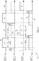
- FIG. 1 is a circuit diagram of an AC-DC power converter 100 according to aspects described herein.
- the converter 100 includes an AC input 101, a rectifier 102 (including diodes D1 107, D2 109, D3 111, and D4 113), a DC bus 104, a DC bus capacitor (Cbus) 106, a first active clamp switch (Sa1) 108, a second active clamp switch (Sa2) 110, a first push-pull switch (Spp1) 112, a second push-pull switch (Spp2) 114, an inductor L1 116, an inductor Lk1 118, an inductor Lk2 120, a transformer (T1) 122, a diode D5 124, a diode D6 126, an output capacitor (C2) 128, and a DC output 130.
- a rectifier 102 including diodes D1 107, D2 109, D3 111, and D4 113
- DC bus 104 DC bus capacitor
- the switches (Sa1 108, Sa2 110, Spp1 112, Spp2 114) in the converter 100 are Metal-Oxide-Semiconductor Field-Effect Transistors (MOSFET); however, in other embodiments, each switch may be another appropriate type of switch or transistor.
- MOSFET Metal-Oxide-Semiconductor Field-Effect Transistors
- the AC input 101 is configured to be coupled to an AC source 103 having a positive and a negative terminal.
- the rectifier 102 is coupled to the AC input 101. More specifically, the anode of diode D1 107 is coupled to the positive terminal of the AC source 103 and to the cathode of diode D3 111.
- the anode of diode D2 109 is coupled to the negative terminal of the AC source 103 and the cathode of diode D4 113.
- the cathodes of diodes D1 107 and D2 109 are coupled to a first terminal of inductor L1 116.
- a second terminal of inductor L1 116 is coupled to a center tap 119 of a primary winding 121 of the transformer (T1) 122.
- the cathodes of diodes D3 111 and D4 113 are coupled to the source of switch Spp1 112 and to the source of switch Spp2 114.
- a negative terminal of the DC bus capacitor (Cbus) 106 is also coupled to the source of switch Spp1 112 and to the source of switch Spp2 114.
- a positive terminal of the DC bus capacitor (Cbus) 106 is coupled to the drains of switches Sa1 108 and Sa2 110 via the DC bus 104.
- the source of switch Sa1 108 is coupled to the drain of switch Spp1 112 and to a first terminal of inductor Lk1 118.
- a second terminal of inductor Lk2 118 is coupled to a first end of the primary winding 121 of the transformer (T1) 122.
- the source of switch Sa2 110 is coupled to the drain of switch Spp2 114 and to a first terminal of inductor Lk2 120.
- a second terminal of inductor Lk2 is coupled to a second end of the primary winding 121 of the transformer (T1) 122.
- a first end of a secondary winding 123 of the transformer (T1) 122 is coupled to the cathode of diode D6 126.
- a second end of the secondary winding 123 of the transformer (T1) 122 is coupled to the cathode of diode D5 124.
- the anodes of diodes D5 125 and D6 126 are coupled to a negative terminal of the output capacitor (C2) 128.
- a center tap 127 of the secondary winding 123 of the transformer (T1) is coupled to a positive terminal of the output capacitor (C2) 128.
- the positive terminal of the output capacitor 128 is also coupled to the output 130.
- the output 130 is configured to be coupled to a load 132.
- the converter 100 also includes a controller 105.
- the controller 105 is coupled to the gates of the switches (Sa1 108, Sa2 110, Spp1 112, Spp2 114) in the converter 100 and is configured to operate the switches via control signals.
- the controller 105 is also coupled to the input 101, the DC bus 104, and the output 130 and is configured to monitor input AC voltage (Vac) provided to the input 101 by the AC source 103, DC voltage (Vbus) on the DC bus 104, and DC voltage (Vout) at the output 130.
- Vac AC voltage
- Vbus DC voltage
- Vout DC voltage
- the controller 105 is further coupled to a current sensor 115 (e.g., a resistor) coupled between the anode of diode D3 and the source of switch Spp1 112 and is configured to monitor current (Iac) through the current sensor 115.
- a current sensor 115 e.g., a resistor
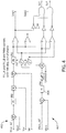
- FIG. 2 is a timing diagram 200 illustrating control signals provided to the switches (Sa1 108, Sa2 110, Spp1 112, Spp2 114) by the controller 105 during operation of the converter 100.
- the timing diagram 200 includes a first trace 202 representing a control signal provided by the controller 105 to the gate of push-pull switch Spp1 112, a second trace 204 representing a control signal provided by the controller 105 to the gate of active clamp switch Sa1 108, a third trace 206 representing a control signal provided by the controller 105 to the gate of push-pull switch Spp2 114, and a fourth trace 208 representing a control signal provided by the controller 105 to the gate of active clamp switch Sa2 110.
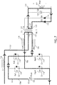
- FIG. 3 includes graphs illustrating different parameters of the converter 100.
- FIG. 3 includes a first graph 300 illustrating the input AC voltage (Vac) during operation of the converter 100, a second graph 302 illustrating current through the current sensor 115 (Iac) during operation of the converter 100, and a third graph 304 illustrating the voltage (Vbus) on the DC bus 104 during operation of the converter 100.
- input AC power (e.g., having an input AC voltage level of 230 Vac) is provided to the input 101 of the converter 100 and the controller 105 monitors the input AC voltage level.
- the controller 105 operates the push-pull switches (Spp1 112 and Spp2 114) and the active clamp switches (Sa1 108 and Sa2 110) in a complementary manner such that the desired DC output voltage (Vout) is provided to a load 132 coupled to the output 130.
- the controller 105 also operates the active clamp switches (Sa1 108 and Sa2 110) to regulate the voltage (Vbus) on the DC bus 104 to a desired level (e.g., 400Vdc). As the voltage (Vbus) on the DC bus 104 approaches the desired level (e.g., 400Vdc as shown in the third graph 304 of FIG. 3 ), the controller 105 operates the active clamp switches (Sa1 108 and Sa2 110) to maintain the voltage (Vbus) on the DC bus 104 at the desired level by reducing the amount of time at which the active clamp switches (Sa1 108 and Sa2 110) are on. For example, as shown in the second trace 204 and the fourth trace 208 of FIG.
- the controller 105 operates the switches Sa1 108 and Sa2 110 to reduce the amount of time at which the switches Sa1 108 and Sa2 110 are on (i.e., reduce the duty cycle of the control signals 204, 208 provided to the switches 108, 110, for example as shown by dashed lines 205, 209). Control of the switches (Spp1 112, Spp2 114, Sa1 108, Sa2 110) by the controller 105 is discussed in greater detail below with respect to FIG. 4 .
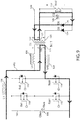
- FIG. 4 is a block diagram illustrating different control loops of the controller 105.
- a first control loop 400 of the controller 105 compares a predefined output voltage reference (Vout_ref) with the actual output voltage (Vout) of the converter 100 and operates the push-pull switches (Spp1 112 and Spp2 114) (i.e., adjusts the pulse width of control signals 202, 206 provided to the gates of the push-pull switches) based on the comparison to drive the output voltage (Vout) of the converter 100 towards the output voltage reference (Vout_ref).
- Vout_ref predefined output voltage reference
- Spp1 112 and Spp2 114 the push-pull switches
- a second control loop 402 of the controller 105 compares a predefined bus voltage reference (Vbus_ref) to the actual voltage (Vbus) on the bus 104 and operates the active clamp switches (Sa1 108 and Sa2 110) (i.e., adjusts the pulse width of control signals 204, 208 provided to the gates of the active clamp switches) based on the comparison to drive the voltage (Vbus) on the bus 104 towards the bus voltage reference (Vbus_ref).
- Vbus_ref bus voltage reference
- Vbus_ref bus voltage reference
- the "turn-on" times of the active clamp switches (Sa1 108 and Sa2 110) can be reduced (e.g., as shown in FIG. 2 ).
- the "turn-on" times of the active clamp switches (Sa1 108 and Sa2 110) are reduced by a factor of K which is defined by the output (PI4) of a Proportional-Integral (PI) controller 404 in the second control loop 402.
- the bus voltage reference (Vbus_ref) is defined at a level such that a desired hold-up time of the output voltage (Vout) can be achieved when input AC power is interrupted.
- FIG. 5 is a timing diagram 500 illustrating control signals provided to the switches (Sa1 108, Sa2 110, Spp1 112, Spp2 114) by the controller 105 during different modes of operation of the converter 100.
- the timing diagram 500 includes a first trace 502 representing a control signal provided by the controller 105 to the gate of push-pull switch Spp1 112, a second trace 504 representing a control signal provided by the controller 105 to the gate of push-pull switch Spp2 114, a third trace 506 representing a control signal provided by the controller 105 to the gate of active clamp switch Sa1 108, and a fourth trace 508 representing a control signal provided by the controller 105 to the gate of active clamp switch Sa2 110.
- FIG. 5 in a first mode of operation, the controller 105 provides a high control signal 502 to the gate of push-pull switch Spp1 112 to operate the switch Spp1 112 to close and low control signals 504, 506, 508 to the gates of switches Spp2 114, Sa1 108, and Sa2 110 to maintain each of the switches 108, 110, 114 in an open state.
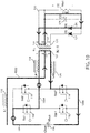
- FIG. 6 is a circuit diagram illustrating operation of a portion of the converter 100 in the first mode of operation. As shown in FIG.
- power derived from the AC input power is provided to the primary winding 121 of the transformer (T1) 122 via a power path 602 including the inductor L1 116, the center tap 119 of the primary winding 121 of the transformer (T1) 122, the inductor Lk1 118, and the push-pull switch Spp1 112.
- the resulting current in the primary winding 121 of the transformer (T1) 122 induces a current in the secondary winding 123 of the transformer (T1) 122 and corresponding DC power having an output DC voltage level (Vout) is provided to the output 130 (i.e., to the load 132 and to the output capacitor (C2) 128 to charge the capacitor).
- the controller 105 in a second mode of operation, provides a high control signal 502 to the gate of push-pull switch Spp1 112 to maintain the switch Spp1 112 in a closed state and a high control signal 508 to the gate of active clamp switch Sa2 110 to operate the switch Sa2 110 to close.
- the controller 105 also provides low control signals 504, 506 to the gates of switches Spp2 114 and Sa1 108 to maintain each of the switches 108, 114 in an open state.
- FIG. 7 is a circuit diagram illustrating operation of a portion of the converter 100 in the second mode of operation. As shown in FIG.
- the second mode of operation power derived from the AC input power is provided to the center tap 119 of the primary winding 121 of the transformer (T1) 122 via a first power path 702 including the inductor L1 116.
- power is also provided from the center tap 119 of the primary winding 121 of the transformer (T1) 122 to the DC bus capacitor (Cbus) 106 via a second power path 704 and back to the rectifier 102 via a third power path 706.
- the second power path 704 includes a portion of the primary winding 121 of the transformer (T1) 122, the inductor Lk2 120, active clamp switch Sa2 110, and the DC bus 104.
- the third power path 706 includes a portion of the primary winding 121 of the transformer (T1) 122, the inductor Lk1 118, and the push-pull switch Spp1 112.
- the current 704 through the active clamp switch Sa2 110 is bidirectional (i.e., can either provide energy to the DC bus capacitor (Cbus) 106 or draw energy from the capacitor 106) depending on whether the voltage (Vbus) across the bus 104 is less than or greater than a voltage level between the primary winding 121 of the transformer (T1) 122 and the inductor Lk2 120.
- Vout DC voltage level
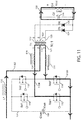
- FIG. 8 is a circuit diagram illustrating operation of a portion of the converter 100 in the third mode of operation.
- power derived from the AC input power is provided to the center tap 119 of the primary winding 121 of the transformer (T1) 122 via a first power path 802 including the inductor L1 116.
- the third mode of operation power is also provided from the center tap 119 of the primary winding 121 of the transformer (T1) 122 to the DC bus capacitor (Cbus) 106 via a second power path 804 and a third power path 806.
- the second power 804 path includes inductor Lk2 120, the active clamp switch Sa2 110, and the DC bus 104.
- the third power path 806 includes inductor Lk1 118, a body diode of active clamp switch Sa1 108, and the DC bus 104.
- the output capacitor (C2) 128 discharges and provides DC power having an output DC voltage level (Vout) to the load 132.
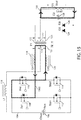
- FIG. 9 is a circuit diagram illustrating operation of a portion of the converter 100 in the fourth mode of operation. As shown in FIG. 5 , in a fourth mode of operation, the controller 105 provides a high control signal 504 to the gate of push-pull switch Spp2 114 to operate the switch Spp2 114 to close and low control signals 502, 506, 508 to the gates of switches Spp1 112, Sa1 108, and Sa2 110 to maintain each of the switches 108, 110, 112 in an open state.
- FIG. 9 is a circuit diagram illustrating operation of a portion of the converter 100 in the fourth mode of operation. As shown in FIG.
- power derived from the AC input power is provided to the primary winding 121 of the transformer (T1) 122 via a power path 902 including the inductor L1 116, the center tap 119 of the primary winding 121 of the transformer (T1) 122, the inductor Lk2 120, and the push-pull switch Spp2 114.
- the resulting current in the primary winding 121 of the transformer (T1) 122 induces a current in the secondary winding 123 of the transformer (T1) 122 and corresponding DC power having an output DC voltage level (Vout) is provided to the output 130 (i.e., to the load 132 and to the output capacitor (C2) 128 to charge the capacitor).
- the controller 105 in a fifth mode of operation, provides a high control signal 504 to the gate of push-pull switch Spp2 114 to maintain the switch Spp2 114 in a closed state and a high control signal 506 to the gate of active clamp switch Sa1 108 to operate the switch Sa1 108 to close.
- the controller 105 also provides low control signals 502, 508 to the gates of switches Spp1 112 and Sa2 110 to maintain each of the switches 110, 112 in an open state.
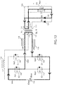
- FIG. 10 is a circuit diagram illustrating operation of a portion of the converter 100 in the fifth mode of operation. As shown in FIG.
- the fifth mode of operation power derived from the AC input power is provided to the center tap 119 of the primary winding 121 of the transformer (T1) 122 via a first power path 1002 including the inductor L1 116.
- power is also provided from the center tap 119 of the primary winding 121 of the transformer (T1) 122 to the DC bus capacitor (Cbus) 106 via a second power path 1004 and back to the rectifier 102 via a third power path 1006.
- the second power path 904 includes a portion of the primary winding 121 of the transformer (T1) 122, the inductor Lk1 118, active clamp switch Sa1 108, and the DC bus 104.
- the third power path 906 includes a portion of the primary winding 121 of the transformer (T1) 122, the inductor Lk2 120, and the push-pull switch Spp2 114.
- the current 904 through the active clamp switch Sa1 108 is bidirectional (i.e., can either provide energy to the DC bus capacitor (Cbus) 106 or draw energy from the capacitor 106) depending on whether the voltage (Vbus) across the bus 104 is less than or greater than a voltage level between the primary winding 121 of the transformer (T1) 122 and the inductor Lk1 118.
- Vout DC voltage level
- the controller 105 provides a high control signal 506 to the gate of active clamp switch Sa1 108 to operate the switch Sa1 108 to close and low control signals 502, 504, 508 to the gates of switches Spp1 112, Spp2, 114, and Sa2 110 to maintain each of the switches 110, 112, 114 in an open state.
- Operation of the converter 100 in the sixth mode of operation is relatively the same as that shown in FIG. 8 .
- power derived from the AC input power is provided to the center tap 119 of the primary winding 121 of the transformer (T1) 122 via a first power path 802 including the inductor L1 116.
- the third mode of operation power is also provided from the center tap 119 of the primary winding 121 of the transformer (T1) 122 to the DC bus capacitor (Cbus) 106 via a second power path 804 and a third power path 806.
- the second power path includes inductor Lk2 120, a body diode of the active clamp switch Sa2 110, and the DC bus 104.
- the third power path includes inductor Lk1 118, the active clamp switch Sa1 108, and the DC bus 104.
- the output capacitor (C2) 128 discharges and provides DC power having an output DC voltage level (Vout) to the load 132.
- the converter may also operate in a seventh mode of operation where the duty ratios of the push-pull switch Spp1 112 and the push-pull switch Spp2 114 are both greater than 0.5.
- the controller 105 provides a high control signal 502 to the gate of push-pull switch Spp1 112 and a high control signal to the gate of push-pull switch Spp2 114 to operate both switches to close.
- the controller 105 also provides low control signals 506, 508 to the gates of switches Sa1 108 and Sa2 110 to maintain each of the switches 108, 110 in an open state.
- FIG. 11 is a circuit diagram illustrating operation of a portion of the converter 100 in the seventh mode of operation.
- the seventh mode of operation power derived from the AC input power is provided to the center tap 119 of the primary winding 121 of the transformer (T1) 122 via a first power path 1102 including the inductor L1 116.
- power is also provided from the center tap 119 of the primary winding 121 of the transformer (T1) 122 to the rectifier 102 via a second power path 1104 and a third power path 1106.
- the second power path 1104 includes inductor Lk1 118 and the push-pull switch Spp1 112.
- the third power path 1106 includes inductor Lk2 120 and a push-pull switch Spp2 114.
- the output capacitor (C2) 128 discharges and provides DC power having an output DC voltage level (Vout) to the load 132.
- the controller 105 operates the converter 100 to maintain a desired voltage (Vout) at the output 130 and to maintain the voltage level (Vbus) on the DC bus 104 at a desired level.
- Vout desired voltage
- Vbus voltage level
- the desired level of the DC bus 104 e.g., Vbus_ref as shown in FIG. 4
- Vout_ref a desired hold-up time of the output voltage (Vout) can be achieved when input AC power is interrupted.
- the controller 105 operates the push-pull switches (Spp1 112 and Spp2 114) and the active clamp switches (Sa1 108 and Sa2 110) in a full-bridge phase shift or full-bridge Pulse Width Modulation (PWM) mode to extend the hold-up time of the converter 100 by drawing energy stored in the DC bus capacitor (Cbus) 106.
- a DC bus capacitor (Cbus) 106 having a capacitance of 250 ⁇ F supplies 1500W for 10ms in a hold-up mode.
- the DC bus capacitor may be configured with another appropriate capacitance. Operation of the converter 100 in a hold-up mode of operation is discussed in greater detail below with respect to FIGS. 12-15 .
- FIGS. 12-15 illustrate operation of the converter 100 in the hold-up mode of operation when the input AC power (Vac) is interrupted.
- FIG. 12 illustrates operation of the converter 100 in a first stage of the hold-up mode of operation
- FIG. 13 illustrates operation of the converter 100 in a second stage of the hold-up mode of operation
- FIG. 14 illustrates operation of the converter 100 in a third stage of the hold-up mode of operation
- FIG. 15 illustrates operation of the converter 100 in a fourth state of the hold-up mode of operation.
- the controller 105 in the first stage of the hold-up mode of operation, provides a high control signal 504 to the gate of push-pull switch Spp2 114 to operate the switch Spp2 114 in a closed state and a high control signal 506 to the gate of active clamp switch Sa1 108 to operate the switch Sa1 108 to close.
- the controller 105 also provides low control signals 502, 508 to the gates of switches Spp1 112 and Sa2 110 to maintain each of the switches in an open state. As shown in FIG.
- power drawn from the DC bus capacitor 106 is provided to the primary winding 121 of the transformer (T1) 122 via a power path 1202 including the DC bus 104, the active clamp switch Sa1 108, the inductor Lk1 118, the primary winding 121 of the transformer (T1) 122, the inductor Lk2 120, and the push-pull switch Spp2 114.
- the resulting current in the primary winding 121 of the transformer (T1) 122 induces a current in the secondary winding 123 of the transformer (T1) 122 and corresponding DC power having an output DC voltage level (Vout) is provided to the output 130 (i.e., to the load 132 and to the output capacitor (C2) 128 to charge the capacitor).
- Vout DC voltage level
- the controller 105 In the second stage of the hold-up mode of operation, the controller 105 provides a high control signal 504 to the gate of push-pull switch Spp2 114 to operate the switch Spp2 114 in a closed state and a high control signal 502 to the gate of push-pull switch Spp1 112 to operate the switch Spp1 112 to close. In the second stage of the hold-up mode of operation, the controller 105 also provides low control signals 506, 508 to the gates of switches Sa1 108 and Sa2 110 to maintain each of the switches in an open state. As shown in FIG. 13 , in the second stage of the hold-up mode operation, the output capacitor (C2) 128 discharges and output DC power having an output DC voltage level (Vout) is provided to the output 130.
- Vout output DC voltage level
- a power path 1302 is generated that includes the push-pull switch Spp1 112, the inductor Lk1 118, the primary winding 121 of the transformer (T1) 122, the inductor Lk2 120, and the push-pull switch Spp2 114.
- the controller 105 provides a high control signal 502 to the gate of push-pull switch Spp1 112 to operate the switch Spp1 112 in a closed state and a high control signal 508 to the gate of active clamp switch Sa2 110 to operate the switch Sa2 110 to close.
- the controller 105 also provides low control signals 504, 506 to the gates of switches Spp2 114 and Sa1 108 to maintain each of the switches in an open state. As shown in FIG.
- power drawn from the DC bus capacitor 106 is provided to the primary winding 121 of the transformer (T1) 122 via a power path 1402 including the DC bus 104, the active clamp switch Sa2 110, the inductor Lk2 120, the primary winding 121 of the transformer (T1) 122, the inductor Lk1 118, and the push-pull switch Spp1 112.
- the resulting current in the primary winding 121 of the transformer (T1) 122 induces a current in the secondary winding 123 of the transformer (T1) 122 and corresponding DC power having an output DC voltage level is provided to the output 130 (i.e., to the load 132 and to the output capacitor (C2) 128 to charge the capacitor).
- the controller 105 provides a high control signal 506 to the gate of active clamp switch Sa1 108 to operate the switch Sa1 108 in a closed state and a high control signal 508 to the gate of active clamp switch Sa2 110 to operate the switch Sa2 110 to close.
- the controller 105 also provides low control signals 502, 504 to the gates of switches Spp1 112 and Spp2 114 to maintain each of the switches in an open state.
- the output capacitor (C2) 128 discharges and DC power having an output DC voltage level (Vout) is provided to the output 130.
- a power path 1502 is generated that includes the active clamp switch Sa2 110, the inductor Lk2 120, the primary winding 121 of the transformer (T1) 122, the inductor Lk1 118, and the active clamp switch Sa1 18.
- the controller 105 can operate the converter 100 to provide DC power at a desired output DC voltage level (Vout) to a load for a hold-up period of time.
- Vout DC voltage level
- a power converter that outputs a constant DC voltage when input AC power is normal and continues to output the constant voltage in a hold-up extension mode of operation when input AC power provided to the converter is interrupted.
- the converter When acceptable input AC power is received, the converter is operated across multiple different modes of operation to maintain a desired voltage (Vout) at the output of the converter.
- Vout desired voltage
- the converter When acceptable input AC power is received, the converter is also operated to maintain a voltage level (Vbus) on a DC bus in the converter at a desired level.
- the desired level of the DC bus can be defined at a level such that a hold-up time of the output voltage (Vout) can be achieved despite the AC power interruption.
- the converter When input AC power is interrupted, the converter is operated across multiple stages of a hold-up mode of operation to draw power from the DC bus and provide DC power at the desired voltage (Vout) to a load for a hold-up period of time. As described above, the converter operates without employing the, typically large and costly, intermediate converters and large bulk capacitors as commonly used in such converters.
Applications Claiming Priority (1)
| Application Number | Priority Date | Filing Date | Title |
|---|---|---|---|
| US15/229,151 US9774263B1 (en) | 2016-08-05 | 2016-08-05 | Power converter with extended hold-up time |
Publications (2)
| Publication Number | Publication Date |
|---|---|
| EP3282571A1 true EP3282571A1 (de) | 2018-02-14 |
| EP3282571B1 EP3282571B1 (de) | 2022-04-20 |
Family
ID=59506143
Family Applications (1)
| Application Number | Title | Priority Date | Filing Date |
|---|---|---|---|
| EP17184171.1A Active EP3282571B1 (de) | 2016-08-05 | 2017-08-01 | Leistungswandler mit verlängerter pufferzeit |
Country Status (3)
| Country | Link |
|---|---|
| US (1) | US9774263B1 (de) |
| EP (1) | EP3282571B1 (de) |
| CN (1) | CN107689736B (de) |
Cited By (1)
| Publication number | Priority date | Publication date | Assignee | Title |
|---|---|---|---|---|
| WO2021021870A1 (en) * | 2019-07-29 | 2021-02-04 | Murata Manufacturing Co., Ltd. | Converter with hold-up circuit and inrush-control circuit |
Families Citing this family (10)
| Publication number | Priority date | Publication date | Assignee | Title |
|---|---|---|---|---|
| WO2018142579A1 (ja) * | 2017-02-03 | 2018-08-09 | 東芝三菱電機産業システム株式会社 | 無停電電源装置 |
| CN106849700A (zh) * | 2017-04-17 | 2017-06-13 | 刘明 | 一种实现零功耗待机开关电源集成电路 |
| JP6708175B2 (ja) * | 2017-07-20 | 2020-06-10 | 株式会社デンソー | 電力変換装置 |
| JP6907852B2 (ja) * | 2017-09-20 | 2021-07-21 | 株式会社デンソー | 電力変換装置 |
| US10367411B2 (en) | 2017-12-20 | 2019-07-30 | Analog Devices Global Unlimited Company | Interleaved boost converter with holdup time extension |
| JP7089377B2 (ja) * | 2018-03-02 | 2022-06-22 | 株式会社豊田中央研究所 | 電力変換装置 |
| US11870249B2 (en) * | 2018-05-24 | 2024-01-09 | Hamilton Sundstrand Corporation | Electrical power system including energy storage modules and shared system controller |
| CN112997391A (zh) * | 2018-11-12 | 2021-06-18 | 住友电气工业株式会社 | 用于半导体开关的驱动设备和驱动方法、功率转换设备以及车辆 |
| CN111106753B (zh) * | 2019-11-29 | 2020-11-06 | 广州金升阳科技有限公司 | 一种推挽变换器的控制电路 |
| US11575326B2 (en) * | 2020-11-27 | 2023-02-07 | Lear Corporation | Wide high voltage-input range DC-DC converter |
Citations (3)
| Publication number | Priority date | Publication date | Assignee | Title |
|---|---|---|---|---|
| US20070247877A1 (en) * | 2006-04-19 | 2007-10-25 | Postech Foundation | Active-clamp current-source push-pull dc-dc converter |
| US20140043861A1 (en) * | 2012-08-08 | 2014-02-13 | Apple Inc. | Controlling an adapter transformer voltage |
| US8791591B1 (en) * | 2010-02-23 | 2014-07-29 | Vlt, Inc. | Zero-current switching multi-output power converter with improved cross-regulation |
Family Cites Families (7)
| Publication number | Priority date | Publication date | Assignee | Title |
|---|---|---|---|---|
| US6504497B2 (en) | 2000-10-30 | 2003-01-07 | Delta Electronics, Inc. | Hold-up-time extension circuits |
| WO2005015718A2 (en) | 2003-08-08 | 2005-02-17 | Astec International Limited | A circuit for maintaining hold-up time while reducing bulk capacitor size and improving efficiency in a power supply |
| WO2010143453A1 (ja) | 2009-06-10 | 2010-12-16 | Nishijima Kimihiro | 力率改善コンバータ |
| CN102904437B (zh) | 2011-07-25 | 2014-08-20 | 台达电子企业管理(上海)有限公司 | 用于电源转换器的维持时间延长电路 |
| US9391532B2 (en) * | 2013-03-14 | 2016-07-12 | Infineon Technologies Ag | System and method for a switched-mode power converter |
| US9407156B2 (en) * | 2013-05-10 | 2016-08-02 | Bose Corporation | Managing leakage inductance in a power supply |
| TWI570546B (zh) * | 2015-01-07 | 2017-02-11 | 群光電能科技股份有限公司 | 具有延長維持時間功能的電源供應裝置 |
-
2016
- 2016-08-05 US US15/229,151 patent/US9774263B1/en active Active
-
2017
- 2017-08-01 EP EP17184171.1A patent/EP3282571B1/de active Active
- 2017-08-02 CN CN201710652534.6A patent/CN107689736B/zh active Active
Patent Citations (3)
| Publication number | Priority date | Publication date | Assignee | Title |
|---|---|---|---|---|
| US20070247877A1 (en) * | 2006-04-19 | 2007-10-25 | Postech Foundation | Active-clamp current-source push-pull dc-dc converter |
| US8791591B1 (en) * | 2010-02-23 | 2014-07-29 | Vlt, Inc. | Zero-current switching multi-output power converter with improved cross-regulation |
| US20140043861A1 (en) * | 2012-08-08 | 2014-02-13 | Apple Inc. | Controlling an adapter transformer voltage |
Non-Patent Citations (2)
| Title |
|---|
| DE OLIVEIRA LEONARDO RUFFEIL ET AL: "Input voltage regulation of an isolated full-bridge boost converter fed by a photovoltaic device with the state-space feedback control method", 2013 BRAZILIAN POWER ELECTRONICS CONFERENCE, IEEE, 27 October 2013 (2013-10-27), pages 595 - 600, XP032585552, ISSN: 2175-8603, [retrieved on 20140409], DOI: 10.1109/COBEP.2013.6785176 * |
| YUNGTAEK JANG ET AL: "Hold-up time extension circuit with integrated magnetics", APPLIED POWER ELECTRONICS CONFERENCE AND EXPOSITION, 2005. APEC 2005. TWENTIETH ANNUAL IEEE AUSTIN, TX, USA 6-10 MARCH 2005, PISCATAWAY, NJ, USA,IEEE, US, vol. 1, 6 March 2005 (2005-03-06), pages 219 - 225Vol.1, XP010809400, ISBN: 978-0-7803-8975-5, DOI: 10.1109/APEC.2005.1452923 * |
Cited By (1)
| Publication number | Priority date | Publication date | Assignee | Title |
|---|---|---|---|---|
| WO2021021870A1 (en) * | 2019-07-29 | 2021-02-04 | Murata Manufacturing Co., Ltd. | Converter with hold-up circuit and inrush-control circuit |
Also Published As
| Publication number | Publication date |
|---|---|
| US9774263B1 (en) | 2017-09-26 |
| EP3282571B1 (de) | 2022-04-20 |
| CN107689736A (zh) | 2018-02-13 |
| CN107689736B (zh) | 2020-01-10 |
Similar Documents
| Publication | Publication Date | Title |
|---|---|---|
| EP3282571A1 (de) | Leistungswandler mit verlängerter pufferzeit | |
| US10574084B2 (en) | Bi-directional DC-DC converter | |
| US10158282B1 (en) | Switching power supply device | |
| US10218256B2 (en) | Primary side control of primary resonant flyback converters | |
| US20180309372A1 (en) | System and method for a switched mode converter | |
| US10693383B2 (en) | Power conversion device | |
| US9973077B2 (en) | Delta conversion rectifier | |
| US8488346B2 (en) | Power conversion apparatus and method | |
| US20120294052A1 (en) | Monotonic pre-bias start-up of a dc-dc converter | |
| EP1872453A2 (de) | Verfahren und vorrichtung zur bereitstellung einer ununterbrechbaren stromversorgung | |
| US9564813B2 (en) | Switching power-supply device | |
| US11283288B2 (en) | Integrated DC to DC converter UPS topology | |
| US10361624B2 (en) | Multi-cell power converter with improved start-up routine | |
| WO2014011259A1 (en) | Circuit and method for providing hold-up time in a dc-dc converter | |
| US8503195B1 (en) | System and method for zero volt switching of half bridge converters during startup and short circuit conditions | |
| US20120014149A1 (en) | Power conversion apparatus and method | |
| US11705753B2 (en) | Integrated PFC and DC DC converter for dual DC bus for online UPS application | |
| US8817490B2 (en) | DC-DC converter | |
| US11387670B2 (en) | Double conversion on line ups with pass through neutral employing single DC bus | |
| US10439512B1 (en) | Clamp circuit to reduce overshoot in power converters | |
| JP2019103200A (ja) | 電力変換装置 | |
| EP4009503A1 (de) | Spannungswandlungsvorrichtung | |
| EP3609070A1 (de) | Hocheffizienter flexibler wandler | |
| CN115473430A (zh) | 电源模组的控制电路、电源模组及电子设备 |
Legal Events
| Date | Code | Title | Description |
|---|---|---|---|
| PUAI | Public reference made under article 153(3) epc to a published international application that has entered the european phase |
Free format text: ORIGINAL CODE: 0009012 |
|
| STAA | Information on the status of an ep patent application or granted ep patent |
Free format text: STATUS: REQUEST FOR EXAMINATION WAS MADE |
|
| 17P | Request for examination filed |
Effective date: 20170801 |
|
| AK | Designated contracting states |
Kind code of ref document: A1 Designated state(s): AL AT BE BG CH CY CZ DE DK EE ES FI FR GB GR HR HU IE IS IT LI LT LU LV MC MK MT NL NO PL PT RO RS SE SI SK SM TR |
|
| AX | Request for extension of the european patent |
Extension state: BA ME |
|
| STAA | Information on the status of an ep patent application or granted ep patent |
Free format text: STATUS: EXAMINATION IS IN PROGRESS |
|
| 17Q | First examination report despatched |
Effective date: 20181024 |
|
| STAA | Information on the status of an ep patent application or granted ep patent |
Free format text: STATUS: EXAMINATION IS IN PROGRESS |
|
| GRAP | Despatch of communication of intention to grant a patent |
Free format text: ORIGINAL CODE: EPIDOSNIGR1 |
|
| STAA | Information on the status of an ep patent application or granted ep patent |
Free format text: STATUS: GRANT OF PATENT IS INTENDED |
|
| RIC1 | Information provided on ipc code assigned before grant |
Ipc: H02M 3/337 20060101AFI20210617BHEP Ipc: H02M 7/217 20060101ALI20210617BHEP Ipc: H02J 7/34 20060101ALI20210617BHEP Ipc: H02J 9/06 20060101ALN20210617BHEP Ipc: H02M 1/00 20060101ALN20210617BHEP Ipc: H02M 1/32 20070101ALN20210617BHEP |
|
| RIC1 | Information provided on ipc code assigned before grant |
Ipc: H02M 3/337 20060101AFI20210624BHEP Ipc: H02M 7/217 20060101ALI20210624BHEP Ipc: H02J 7/34 20060101ALI20210624BHEP Ipc: H02J 9/06 20060101ALN20210624BHEP Ipc: H02M 1/00 20060101ALN20210624BHEP Ipc: H02M 1/32 20070101ALN20210624BHEP |
|
| INTG | Intention to grant announced |
Effective date: 20210712 |
|
| GRAJ | Information related to disapproval of communication of intention to grant by the applicant or resumption of examination proceedings by the epo deleted |
Free format text: ORIGINAL CODE: EPIDOSDIGR1 |
|
| STAA | Information on the status of an ep patent application or granted ep patent |
Free format text: STATUS: EXAMINATION IS IN PROGRESS |
|
| INTC | Intention to grant announced (deleted) | ||
| GRAP | Despatch of communication of intention to grant a patent |
Free format text: ORIGINAL CODE: EPIDOSNIGR1 |
|
| STAA | Information on the status of an ep patent application or granted ep patent |
Free format text: STATUS: GRANT OF PATENT IS INTENDED |
|
| RIC1 | Information provided on ipc code assigned before grant |
Ipc: H02M 1/32 20070101ALN20211110BHEP Ipc: H02M 1/00 20060101ALN20211110BHEP Ipc: H02J 9/06 20060101ALN20211110BHEP Ipc: H02J 7/34 20060101ALI20211110BHEP Ipc: H02M 7/217 20060101ALI20211110BHEP Ipc: H02M 3/337 20060101AFI20211110BHEP |
|
| INTG | Intention to grant announced |
Effective date: 20211126 |
|
| RIC1 | Information provided on ipc code assigned before grant |
Ipc: H02M 1/32 20070101ALN20211115BHEP Ipc: H02M 1/00 20060101ALN20211115BHEP Ipc: H02J 9/06 20060101ALN20211115BHEP Ipc: H02J 7/34 20060101ALI20211115BHEP Ipc: H02M 7/217 20060101ALI20211115BHEP Ipc: H02M 3/337 20060101AFI20211115BHEP |
|
| GRAS | Grant fee paid |
Free format text: ORIGINAL CODE: EPIDOSNIGR3 |
|
| GRAA | (expected) grant |
Free format text: ORIGINAL CODE: 0009210 |
|
| STAA | Information on the status of an ep patent application or granted ep patent |
Free format text: STATUS: THE PATENT HAS BEEN GRANTED |
|
| AK | Designated contracting states |
Kind code of ref document: B1 Designated state(s): AL AT BE BG CH CY CZ DE DK EE ES FI FR GB GR HR HU IE IS IT LI LT LU LV MC MK MT NL NO PL PT RO RS SE SI SK SM TR |
|
| RAP3 | Party data changed (applicant data changed or rights of an application transferred) |
Owner name: SCHNEIDER ELECTRIC IT CORPORATION |
|
| REG | Reference to a national code |
Ref country code: GB Ref legal event code: FG4D |
|
| REG | Reference to a national code |
Ref country code: CH Ref legal event code: EP |
|
| REG | Reference to a national code |
Ref country code: IE Ref legal event code: FG4D |
|
| REG | Reference to a national code |
Ref country code: DE Ref legal event code: R096 Ref document number: 602017056163 Country of ref document: DE |
|
| REG | Reference to a national code |
Ref country code: AT Ref legal event code: REF Ref document number: 1485983 Country of ref document: AT Kind code of ref document: T Effective date: 20220515 |
|
| REG | Reference to a national code |
Ref country code: LT Ref legal event code: MG9D |
|
| REG | Reference to a national code |
Ref country code: NL Ref legal event code: MP Effective date: 20220420 |
|
| REG | Reference to a national code |
Ref country code: AT Ref legal event code: MK05 Ref document number: 1485983 Country of ref document: AT Kind code of ref document: T Effective date: 20220420 |
|
| PG25 | Lapsed in a contracting state [announced via postgrant information from national office to epo] |
Ref country code: NL Free format text: LAPSE BECAUSE OF FAILURE TO SUBMIT A TRANSLATION OF THE DESCRIPTION OR TO PAY THE FEE WITHIN THE PRESCRIBED TIME-LIMIT Effective date: 20220420 |
|
| PG25 | Lapsed in a contracting state [announced via postgrant information from national office to epo] |
Ref country code: SE Free format text: LAPSE BECAUSE OF FAILURE TO SUBMIT A TRANSLATION OF THE DESCRIPTION OR TO PAY THE FEE WITHIN THE PRESCRIBED TIME-LIMIT Effective date: 20220420 Ref country code: PT Free format text: LAPSE BECAUSE OF FAILURE TO SUBMIT A TRANSLATION OF THE DESCRIPTION OR TO PAY THE FEE WITHIN THE PRESCRIBED TIME-LIMIT Effective date: 20220822 Ref country code: NO Free format text: LAPSE BECAUSE OF FAILURE TO SUBMIT A TRANSLATION OF THE DESCRIPTION OR TO PAY THE FEE WITHIN THE PRESCRIBED TIME-LIMIT Effective date: 20220720 Ref country code: LT Free format text: LAPSE BECAUSE OF FAILURE TO SUBMIT A TRANSLATION OF THE DESCRIPTION OR TO PAY THE FEE WITHIN THE PRESCRIBED TIME-LIMIT Effective date: 20220420 Ref country code: HR Free format text: LAPSE BECAUSE OF FAILURE TO SUBMIT A TRANSLATION OF THE DESCRIPTION OR TO PAY THE FEE WITHIN THE PRESCRIBED TIME-LIMIT Effective date: 20220420 Ref country code: GR Free format text: LAPSE BECAUSE OF FAILURE TO SUBMIT A TRANSLATION OF THE DESCRIPTION OR TO PAY THE FEE WITHIN THE PRESCRIBED TIME-LIMIT Effective date: 20220721 Ref country code: FI Free format text: LAPSE BECAUSE OF FAILURE TO SUBMIT A TRANSLATION OF THE DESCRIPTION OR TO PAY THE FEE WITHIN THE PRESCRIBED TIME-LIMIT Effective date: 20220420 Ref country code: ES Free format text: LAPSE BECAUSE OF FAILURE TO SUBMIT A TRANSLATION OF THE DESCRIPTION OR TO PAY THE FEE WITHIN THE PRESCRIBED TIME-LIMIT Effective date: 20220420 Ref country code: BG Free format text: LAPSE BECAUSE OF FAILURE TO SUBMIT A TRANSLATION OF THE DESCRIPTION OR TO PAY THE FEE WITHIN THE PRESCRIBED TIME-LIMIT Effective date: 20220720 Ref country code: AT Free format text: LAPSE BECAUSE OF FAILURE TO SUBMIT A TRANSLATION OF THE DESCRIPTION OR TO PAY THE FEE WITHIN THE PRESCRIBED TIME-LIMIT Effective date: 20220420 |
|
| PG25 | Lapsed in a contracting state [announced via postgrant information from national office to epo] |
Ref country code: RS Free format text: LAPSE BECAUSE OF FAILURE TO SUBMIT A TRANSLATION OF THE DESCRIPTION OR TO PAY THE FEE WITHIN THE PRESCRIBED TIME-LIMIT Effective date: 20220420 Ref country code: PL Free format text: LAPSE BECAUSE OF FAILURE TO SUBMIT A TRANSLATION OF THE DESCRIPTION OR TO PAY THE FEE WITHIN THE PRESCRIBED TIME-LIMIT Effective date: 20220420 Ref country code: LV Free format text: LAPSE BECAUSE OF FAILURE TO SUBMIT A TRANSLATION OF THE DESCRIPTION OR TO PAY THE FEE WITHIN THE PRESCRIBED TIME-LIMIT Effective date: 20220420 Ref country code: IS Free format text: LAPSE BECAUSE OF FAILURE TO SUBMIT A TRANSLATION OF THE DESCRIPTION OR TO PAY THE FEE WITHIN THE PRESCRIBED TIME-LIMIT Effective date: 20220820 |
|
| REG | Reference to a national code |
Ref country code: DE Ref legal event code: R097 Ref document number: 602017056163 Country of ref document: DE |
|
| PG25 | Lapsed in a contracting state [announced via postgrant information from national office to epo] |
Ref country code: SM Free format text: LAPSE BECAUSE OF FAILURE TO SUBMIT A TRANSLATION OF THE DESCRIPTION OR TO PAY THE FEE WITHIN THE PRESCRIBED TIME-LIMIT Effective date: 20220420 Ref country code: SK Free format text: LAPSE BECAUSE OF FAILURE TO SUBMIT A TRANSLATION OF THE DESCRIPTION OR TO PAY THE FEE WITHIN THE PRESCRIBED TIME-LIMIT Effective date: 20220420 Ref country code: RO Free format text: LAPSE BECAUSE OF FAILURE TO SUBMIT A TRANSLATION OF THE DESCRIPTION OR TO PAY THE FEE WITHIN THE PRESCRIBED TIME-LIMIT Effective date: 20220420 Ref country code: EE Free format text: LAPSE BECAUSE OF FAILURE TO SUBMIT A TRANSLATION OF THE DESCRIPTION OR TO PAY THE FEE WITHIN THE PRESCRIBED TIME-LIMIT Effective date: 20220420 Ref country code: DK Free format text: LAPSE BECAUSE OF FAILURE TO SUBMIT A TRANSLATION OF THE DESCRIPTION OR TO PAY THE FEE WITHIN THE PRESCRIBED TIME-LIMIT Effective date: 20220420 Ref country code: CZ Free format text: LAPSE BECAUSE OF FAILURE TO SUBMIT A TRANSLATION OF THE DESCRIPTION OR TO PAY THE FEE WITHIN THE PRESCRIBED TIME-LIMIT Effective date: 20220420 |
|
| PLBE | No opposition filed within time limit |
Free format text: ORIGINAL CODE: 0009261 |
|
| STAA | Information on the status of an ep patent application or granted ep patent |
Free format text: STATUS: NO OPPOSITION FILED WITHIN TIME LIMIT |
|
| 26N | No opposition filed |
Effective date: 20230123 |
|
| PG25 | Lapsed in a contracting state [announced via postgrant information from national office to epo] |
Ref country code: MC Free format text: LAPSE BECAUSE OF FAILURE TO SUBMIT A TRANSLATION OF THE DESCRIPTION OR TO PAY THE FEE WITHIN THE PRESCRIBED TIME-LIMIT Effective date: 20220420 Ref country code: AL Free format text: LAPSE BECAUSE OF FAILURE TO SUBMIT A TRANSLATION OF THE DESCRIPTION OR TO PAY THE FEE WITHIN THE PRESCRIBED TIME-LIMIT Effective date: 20220420 |
|
| REG | Reference to a national code |
Ref country code: CH Ref legal event code: PL |
|
| PG25 | Lapsed in a contracting state [announced via postgrant information from national office to epo] |
Ref country code: LU Free format text: LAPSE BECAUSE OF NON-PAYMENT OF DUE FEES Effective date: 20220801 Ref country code: LI Free format text: LAPSE BECAUSE OF NON-PAYMENT OF DUE FEES Effective date: 20220831 Ref country code: CH Free format text: LAPSE BECAUSE OF NON-PAYMENT OF DUE FEES Effective date: 20220831 |
|
| REG | Reference to a national code |
Ref country code: BE Ref legal event code: MM Effective date: 20220831 |
|
| PG25 | Lapsed in a contracting state [announced via postgrant information from national office to epo] |
Ref country code: SI Free format text: LAPSE BECAUSE OF FAILURE TO SUBMIT A TRANSLATION OF THE DESCRIPTION OR TO PAY THE FEE WITHIN THE PRESCRIBED TIME-LIMIT Effective date: 20220420 |
|
| PG25 | Lapsed in a contracting state [announced via postgrant information from national office to epo] |
Ref country code: IE Free format text: LAPSE BECAUSE OF NON-PAYMENT OF DUE FEES Effective date: 20220801 |
|
| PG25 | Lapsed in a contracting state [announced via postgrant information from national office to epo] |
Ref country code: BE Free format text: LAPSE BECAUSE OF NON-PAYMENT OF DUE FEES Effective date: 20220831 |
|
| PGFP | Annual fee paid to national office [announced via postgrant information from national office to epo] |
Ref country code: GB Payment date: 20230822 Year of fee payment: 7 |
|
| PGFP | Annual fee paid to national office [announced via postgrant information from national office to epo] |
Ref country code: FR Payment date: 20230824 Year of fee payment: 7 Ref country code: DE Payment date: 20230828 Year of fee payment: 7 |
|
| PG25 | Lapsed in a contracting state [announced via postgrant information from national office to epo] |
Ref country code: IT Free format text: LAPSE BECAUSE OF FAILURE TO SUBMIT A TRANSLATION OF THE DESCRIPTION OR TO PAY THE FEE WITHIN THE PRESCRIBED TIME-LIMIT Effective date: 20220420 |
|
| PG25 | Lapsed in a contracting state [announced via postgrant information from national office to epo] |
Ref country code: HU Free format text: LAPSE BECAUSE OF FAILURE TO SUBMIT A TRANSLATION OF THE DESCRIPTION OR TO PAY THE FEE WITHIN THE PRESCRIBED TIME-LIMIT; INVALID AB INITIO Effective date: 20170801 |
|
| PG25 | Lapsed in a contracting state [announced via postgrant information from national office to epo] |
Ref country code: MK Free format text: LAPSE BECAUSE OF FAILURE TO SUBMIT A TRANSLATION OF THE DESCRIPTION OR TO PAY THE FEE WITHIN THE PRESCRIBED TIME-LIMIT Effective date: 20220420 Ref country code: CY Free format text: LAPSE BECAUSE OF FAILURE TO SUBMIT A TRANSLATION OF THE DESCRIPTION OR TO PAY THE FEE WITHIN THE PRESCRIBED TIME-LIMIT Effective date: 20220420 |