EP3282483A1 - Pixel unit and method for preparing the same, array substrate and display device - Google Patents
Pixel unit and method for preparing the same, array substrate and display device Download PDFInfo
- Publication number
- EP3282483A1 EP3282483A1 EP17737196.0A EP17737196A EP3282483A1 EP 3282483 A1 EP3282483 A1 EP 3282483A1 EP 17737196 A EP17737196 A EP 17737196A EP 3282483 A1 EP3282483 A1 EP 3282483A1
- Authority
- EP
- European Patent Office
- Prior art keywords
- pixel
- layer
- light emitting
- hole
- emitting layer
- Prior art date
- Legal status (The legal status is an assumption and is not a legal conclusion. Google has not performed a legal analysis and makes no representation as to the accuracy of the status listed.)
- Withdrawn
Links
Images



Classifications
-
- H—ELECTRICITY
- H10—SEMICONDUCTOR DEVICES; ELECTRIC SOLID-STATE DEVICES NOT OTHERWISE PROVIDED FOR
- H10K—ORGANIC ELECTRIC SOLID-STATE DEVICES
- H10K59/00—Integrated devices, or assemblies of multiple devices, comprising at least one organic light-emitting element covered by group H10K50/00
- H10K59/10—OLED displays
- H10K59/12—Active-matrix OLED [AMOLED] displays
- H10K59/122—Pixel-defining structures or layers, e.g. banks
-
- G—PHYSICS
- G09—EDUCATION; CRYPTOGRAPHY; DISPLAY; ADVERTISING; SEALS
- G09F—DISPLAYING; ADVERTISING; SIGNS; LABELS OR NAME-PLATES; SEALS
- G09F9/00—Indicating arrangements for variable information in which the information is built-up on a support by selection or combination of individual elements
- G09F9/30—Indicating arrangements for variable information in which the information is built-up on a support by selection or combination of individual elements in which the desired character or characters are formed by combining individual elements
- G09F9/33—Indicating arrangements for variable information in which the information is built-up on a support by selection or combination of individual elements in which the desired character or characters are formed by combining individual elements being semiconductor devices, e.g. diodes
-
- H—ELECTRICITY
- H10—SEMICONDUCTOR DEVICES; ELECTRIC SOLID-STATE DEVICES NOT OTHERWISE PROVIDED FOR
- H10D—INORGANIC ELECTRIC SEMICONDUCTOR DEVICES
- H10D86/00—Integrated devices formed in or on insulating or conducting substrates, e.g. formed in silicon-on-insulator [SOI] substrates or on stainless steel or glass substrates
-
- H—ELECTRICITY
- H10—SEMICONDUCTOR DEVICES; ELECTRIC SOLID-STATE DEVICES NOT OTHERWISE PROVIDED FOR
- H10D—INORGANIC ELECTRIC SEMICONDUCTOR DEVICES
- H10D86/00—Integrated devices formed in or on insulating or conducting substrates, e.g. formed in silicon-on-insulator [SOI] substrates or on stainless steel or glass substrates
- H10D86/40—Integrated devices formed in or on insulating or conducting substrates, e.g. formed in silicon-on-insulator [SOI] substrates or on stainless steel or glass substrates characterised by multiple TFTs
-
- H—ELECTRICITY
- H10—SEMICONDUCTOR DEVICES; ELECTRIC SOLID-STATE DEVICES NOT OTHERWISE PROVIDED FOR
- H10D—INORGANIC ELECTRIC SEMICONDUCTOR DEVICES
- H10D86/00—Integrated devices formed in or on insulating or conducting substrates, e.g. formed in silicon-on-insulator [SOI] substrates or on stainless steel or glass substrates
- H10D86/40—Integrated devices formed in or on insulating or conducting substrates, e.g. formed in silicon-on-insulator [SOI] substrates or on stainless steel or glass substrates characterised by multiple TFTs
- H10D86/60—Integrated devices formed in or on insulating or conducting substrates, e.g. formed in silicon-on-insulator [SOI] substrates or on stainless steel or glass substrates characterised by multiple TFTs wherein the TFTs are in active matrices
-
- H—ELECTRICITY
- H10—SEMICONDUCTOR DEVICES; ELECTRIC SOLID-STATE DEVICES NOT OTHERWISE PROVIDED FOR
- H10K—ORGANIC ELECTRIC SOLID-STATE DEVICES
- H10K50/00—Organic light-emitting devices
- H10K50/80—Constructional details
- H10K50/805—Electrodes
- H10K50/81—Anodes
- H10K50/813—Anodes characterised by their shape
-
- H—ELECTRICITY
- H10—SEMICONDUCTOR DEVICES; ELECTRIC SOLID-STATE DEVICES NOT OTHERWISE PROVIDED FOR
- H10K—ORGANIC ELECTRIC SOLID-STATE DEVICES
- H10K50/00—Organic light-emitting devices
- H10K50/80—Constructional details
- H10K50/805—Electrodes
- H10K50/82—Cathodes
- H10K50/822—Cathodes characterised by their shape
-
- H—ELECTRICITY
- H10—SEMICONDUCTOR DEVICES; ELECTRIC SOLID-STATE DEVICES NOT OTHERWISE PROVIDED FOR
- H10K—ORGANIC ELECTRIC SOLID-STATE DEVICES
- H10K59/00—Integrated devices, or assemblies of multiple devices, comprising at least one organic light-emitting element covered by group H10K50/00
- H10K59/10—OLED displays
- H10K59/12—Active-matrix OLED [AMOLED] displays
- H10K59/1201—Manufacture or treatment
-
- H—ELECTRICITY
- H10—SEMICONDUCTOR DEVICES; ELECTRIC SOLID-STATE DEVICES NOT OTHERWISE PROVIDED FOR
- H10K—ORGANIC ELECTRIC SOLID-STATE DEVICES
- H10K59/00—Integrated devices, or assemblies of multiple devices, comprising at least one organic light-emitting element covered by group H10K50/00
- H10K59/10—OLED displays
- H10K59/12—Active-matrix OLED [AMOLED] displays
- H10K59/121—Active-matrix OLED [AMOLED] displays characterised by the geometry or disposition of pixel elements
- H10K59/1213—Active-matrix OLED [AMOLED] displays characterised by the geometry or disposition of pixel elements the pixel elements being TFTs
-
- H—ELECTRICITY
- H10—SEMICONDUCTOR DEVICES; ELECTRIC SOLID-STATE DEVICES NOT OTHERWISE PROVIDED FOR
- H10K—ORGANIC ELECTRIC SOLID-STATE DEVICES
- H10K59/00—Integrated devices, or assemblies of multiple devices, comprising at least one organic light-emitting element covered by group H10K50/00
- H10K59/80—Constructional details
- H10K59/805—Electrodes
- H10K59/8051—Anodes
- H10K59/80515—Anodes characterised by their shape
-
- H—ELECTRICITY
- H10—SEMICONDUCTOR DEVICES; ELECTRIC SOLID-STATE DEVICES NOT OTHERWISE PROVIDED FOR
- H10K—ORGANIC ELECTRIC SOLID-STATE DEVICES
- H10K59/00—Integrated devices, or assemblies of multiple devices, comprising at least one organic light-emitting element covered by group H10K50/00
- H10K59/80—Constructional details
- H10K59/805—Electrodes
- H10K59/8052—Cathodes
- H10K59/80521—Cathodes characterised by their shape
-
- H—ELECTRICITY
- H10—SEMICONDUCTOR DEVICES; ELECTRIC SOLID-STATE DEVICES NOT OTHERWISE PROVIDED FOR
- H10K—ORGANIC ELECTRIC SOLID-STATE DEVICES
- H10K50/00—Organic light-emitting devices
- H10K50/80—Constructional details
- H10K50/805—Electrodes
-
- H—ELECTRICITY
- H10—SEMICONDUCTOR DEVICES; ELECTRIC SOLID-STATE DEVICES NOT OTHERWISE PROVIDED FOR
- H10K—ORGANIC ELECTRIC SOLID-STATE DEVICES
- H10K59/00—Integrated devices, or assemblies of multiple devices, comprising at least one organic light-emitting element covered by group H10K50/00
- H10K59/80—Constructional details
- H10K59/805—Electrodes
Definitions
- the present invention generally relates to the field of display technology, and particularly to a pixel unit used in an organic light emitting diode display apparatus, a method of manufacturing the same, an array substrate and a display apparatus.
- OLED Organic light emitting diode display apparatus
- TFT thin film transistors
- LTPS-TFT low-temperature polycrystalline silicon thin film transistors
- At least one object of the present invention is to provide a pixel unit which can avoid occurrence of color mixing phenomenon and of which a manufacturing method is simple in the process, and low in the cost, and has no influence on the luminous effect.
- a further object of the present invention is to provide a method of manufacturing a pixel unit.
- the pixel unit can avoid occurrence of color mixing phenomenon and the method is simple in the process, and low in the cost, and has no influence on the luminous effect.
- Another object of the present invention is to provide an array substrate in which the pixel unit can avoid occurrence of color mixing phenomenon and of which a manufacturing method is simple in the process, and low in the cost, and has no influence on the luminous effect.
- Yet another object of the present invention is to provide a display apparatus in which the pixel unit can avoid occurrence of color mixing phenomenon and of which a manufacturing method is simple in the process, and low in the cost, and has no influence on the luminous effect.
- a pixel unit comprising: a pixel definition layer, a pixel electrode, a light emitting layer and a common electrode; wherein, the pixel definition layer has a firs through hole, within which the pixel electrode, the light emitting layer and the common electrode are laminated; the pixel electrode comprises a bottom surface portion and a side surface portion, the side surface portion extending to a top of a side wall of the first through hole on the side wall of the first through hole; the light emitting layer is formed on the pixel electrode and covers over the pixel electrode; and the common electrode is formed on the light emitting layer, covers over the light emitting layer and extends on a top surface of the pixel definition layer.
- the side wall of the first through hole in the pixel definition layer is formed as a flat face, an outwardly cambered face, or an inwardly cambered face or in a step shape.
- the pixel electrode extends to the top surface of the pixel definition layer, an end of the pixel electrode is on the top surface of the pixel definition layer, and, both an end of the light emitting layer and an end of the common electrode have a step shape.
- the pixel unit further comprises: a protective layer formed on the pixel definition layer and covering over an end of the pixel electrode, wherein the light emitting layer covers over the protective layer.
- the pixel unit further comprises: a planarization layer having a second through hole at a location corresponding to an output terminal of a driver thin film transistor, wherein the pixel definition layer is formed on the planarization layer, and the first through hole is located directly above the second through hole and is communicated with the second through hole.
- an array substrate comprising: any of the abovementioned pixel units.
- a display apparatus comprising: the abovementioned array substrate.
- a method of manufacturing a pixel unit and, the method is used for manufacturing the pixel unit of claim 1 and comprises: forming a pixel definition layer and forming a first through hole in the pixel definition layer; forming a pixel electrode within the first through hole of the pixel definition layer, the pixel electrode having a bottom surface and a side surface, and the side surface extending to a top of a side wall of the first through hole on the side wall of the first through hole; forming a light emitting layer that covers over the pixel electrode; and forming a common electrode that covers over the light emitting layer and extends on a top surface of the pixel definition layer.
- the forming the pixel definition layer and the forming the first through hole in the pixel definition layer comprises: depositing two layers of organic material in sequence, and forming, by one patterning process, a second through hole in the planarization layer and the first through hole in the pixel definition layer
- the method further comprises: depositing an organic material on the pixel definition layer, and, forming, by one patterning process, a spacer layer and a protective layer that covers over an end of the pixel electrode; and the forming the light emitting layer that covers over the pixel electrode further comprises: forming the light emitting layer on the pixel electrode such that the light emitting layer covers over the pixel electrode and the protective layer.
- the pixel unit generally includes a low-temperature polycrystalline silicon thin film transistor served as a thin film transistor 100 for driving, a planarization layer 200, a pixel definition layer 300, a pixel electrode 400, a light emitting layer 500 and a common electrode 600, and so on. Both side surfaces of the light emitting layer 500 are contacted directly with the pixel definition layer 300. A light emitted by the light emitting layer 500 scatters to the surroundings after passing through the pixel definition layer 300 and makes a color mixing with the lights scattered from other pixel units around this pixel unit, to seriously affect the display effect.
- LTPS-TFT OLED organic light emitting diode
- a polycrystalline silicon (Poly), a gate insulation layer (Gate 1), a gate (Gate 2), an interlayer deposition layer (ILD), a source and a drain (SD), a planarization layer (PLN), a pixel electrode (Anode), a pixel definition layer (PDL), a spacer layer (PS), a light emitting layer evaporation (EL) and a common electrode (Vcom) are manufactured in sequence.
- Fig. 2 shows a structural schematic view of a pixel unit according to a first embodiment of the present invention.
- the pixel unit is formed on a driver thin film transistor and includes: a planarization layer (PLN layer) 200, a pixel definition layer (PDL layer) 300, a pixel electrode 400, a light emitting layer 500 and a common electrode 600.
- PNL layer planarization layer
- PDL layer pixel definition layer
- a pixel electrode 400 a light emitting layer 500 and a common electrode 600.
- the driver thin film transistor may be a low-temperature polycrystalline silicon thin film transistor which includes a substrate 101, a buffer layer 102 formed on the substrate 101, an output electrode 103, a channel 104 and an input electrode 105 formed on the buffer layer 102, a gate insulation layer 106 formed on the buffer layer 102 as well as the output electrode 103, the channel 104 and the input electrode 105, a control terminal 107 formed on the gate insulation layer 106, and, an interlayer deposition layer 108 (ILD layer) formed on the control terminal 107 and the gate insulation layer 106.
- ILD layer interlayer deposition layer
- a third through hole 111 and a fourth through hole 112 running through the interlayer deposition layer 108 and the gate insulation layer 106 are formed directly above the output electrode 103 and the input electrode 105, respectively.
- An output terminal 109 has one end connected to the output electrode 103 and led out through the third through hole 111, and the other end exposed on the interlayer deposition layer 108, and, the input terminal 110 has one end connected to the input electrode 105 and led out through the fourth through hole 112, and the other end exposed on the interlayer deposition layer 108.
- the control terminal 107 is embodied as a gate of the driver thin film transistor, the input electrode 105 is embodied as a drain, the input terminal 110 is embodied as a drain metal, the output electrode 103 is embodied as a source and the output terminal 109 is embodied as a source metal.
- the control terminal 107 is embodied as a gate of the driver thin film transistor, the input electrode 105 is embodied as a source, the input terminal 110 is embodied as a source metal, the output electrode 103 is embodied as a drain and the output terminal 109 is embodied as a drain metal.
- the planarization layer 200 is formed on the interlayer deposition layer 108, as well as on the output terminal 109 and the input terminal 110, of the driver thin film transistor, and has a second through hole 201 directly above the output terminal 109.
- the pixel definition layer 300 is formed on the planarization layer 200, and has a first through hole 301 directly above the second through hole 201.
- the first through hole 301 has a greater size than the second through hole 201, and is communicated with the second through hole 201.
- a pixel electrode 400, a light emitting layer 500 and a common electrode 600 are formed in sequence on the pixel definition layer 300.
- the pixel electrode 400 comprises a bottom surface portion and a side surface portion. The bottom surface portion overspreads the bottom of the first through hole 301 and is connected with the output terminal 109 through the second through hole 201, and the side surface portion extends to a top of a side wall 302 of the first through hole 301 on the side wall 302 of the first through hole 301.
- the light emitting layer 500 is formed on the pixel electrode 400 and covers over the pixel electrode layer 400.
- the common electrode 600 is formed on the light emitting layer 500 and covers over the light emitting layer 500 and extends on a top surface of the pixel definition layer 300.
- the pixel electrode 400 comprises a reflective electrode formed of indium tin oxide / silver / indium tin oxide (ITO/Ag/ITO) material, or of lightproof conductive material.
- the pixel electrode 400 is provided between the pixel definition layer 300 and the light emitting layer 500, and a light emitted by the light emitting layer 500 are partially reflected by the reflective electrode formed of indium tin oxide / silver / indium tin oxide (ITO/Ag/ITO) material, or are blocked by the lightproof conductive material, so that scattering of a light from the light emitting layer 500 to the surroundings is greatly reduced, thereby greatly alleviating color mixing phenomenon occurred between the pixel units, to effectively solve the color mixing problem brought by scatting of the light.
- ITO/Ag/ITO indium tin oxide
- the pixel electrode 400 includes the side surface portion, which enables area of the pixel electrode 400 to be increased, so that contact area between the pixel electrode 400 and the light emitting layer 500 is increased, and accordingly luminous area of the pixel unit is increased without changing aperture ratio of the pixel unit, thereby enhancing overall luminance.
- the substrate 101 includes a glass material
- the buffer layer 102 includes silicon nitride (SiN x ) or silicon dioxide (SiO 2 ) or aluminum (Al) or aluminum oxide (AL 2 O 3 ) material
- the output electrode 103, the channel 104 and the input electrode 105 are polycrystalline silicon (P-Si) material
- the gate insulation layer 106 includes silicon dioxide (SiO 2 ) or bilayer material consisted of silicon dioxide (SiO 2 )/silicon nitride (SiN x ) or TEOS material
- the control terminal 107 includes molybdenum niobium material
- the output terminal 109 and the input terminal 110 includes Ti-Al-Ti material
- the interlayer deposition layer 108 includes silicon nitride (SiN x ) or silicon dioxide (SiO 2 ) material
- the planarization layer 200 includes an organic film material
- the pixel definition layer 300 includes polyimide (PI) material
- the light emitting layer 500
- the pixel electrode 400 may further extend to the top surface of the pixel definition layer 300, and an end of the pixel electrode 400 is located on the top surface of the pixel definition layer 300.
- An end 501 of the light emitting layer has a step shape and covers over the end of the pixel electrode 400.
- An end 601 of the common electrode has a step shape and covers over the end 501 of the light emitting layer and extends on the top surface of the pixel definition layer 300.
- Fig. 3 shows a structural schematic view of a pixel unit according to a second embodiment of the present invention.
- technical features of the first embodiment which can be employed in the second embodiment are incorporated herein by reference, but are omitted to avoid duplicating description. The following description only relates to these technical features of the second embodiment different from the first embodiment.
- the side wall 302 of the first through hole 301 in the pixel definition layer 300 has an outwardly cambered face, and the side surface of the pixel electrode 400 extends to the top of the side wall 302 of the first through hole 301 on the outwardly cambered face of the side wall 302 of the first through hole 301.
- the light emitting layer 500 is formed on the pixel electrode 400 and covers over the pixel definition layer 300.
- the common electrode 600 is formed on the light emitting layer 500 and covers over the light emitting layer 500 and extends on the top surface of the pixel definition layer 300.
- the area of the side wall 302 of the first through hole 301 in the pixel unit according to the second embodiment is greater than that of the side wall 302 of the first through hole 301 in the pixel unit according to the first embodiment, which further increases the areas of the pixel electrode 400 and the light emitting layer 500, so that the contact area between the pixel electrode 400 and the light emitting layer 500 is further increased, and accordingly, overall luminance of the pixel unit is further enhanced without changing aperture ratio of the pixel unit, while avoiding the color mixing problem caused by scattering of the light.
- the pixel electrode 400 may further extend to the top surface of the pixel definition layer 300, and an end of the pixel electrode 400 is located on the top surface of the pixel definition layer 300.
- An end 501 of the light emitting layer has a step shape and covers over the end of the pixel electrode 400.
- the end 601 of the common electrode has a step shape and covers over the end 501 of the light emitting layer and extends on the top surface of the pixel definition layer 300.
- Fig. 4 shows a structural schematic view of a pixel unit according to a third embodiment of the present invention.
- technical features of any one of the above embodiments which can be employed in the third embodiment are incorporated herein by reference, but are omitted to avoid duplicating description. The following description only relates to these technical features of the third embodiment different from other embodiments.
- the side wall 302 of the first through hole 301 in the pixel definition layer 300 has an inwardly cambered face, and the side surface of the pixel electrode 400 extends to the top of the side wall 302 of the first through hole 301 on the inwardly cambered face of the side wall 302 of the first through hole 301.
- the light emitting layer 500 is formed on the pixel electrode 400 and covers over the pixel definition layer 300.
- the common electrode 600 is formed on the light emitting layer 500 and covers over the light emitting layer 500 and extends on the top surface of the pixel definition layer 300.
- the area of the side wall 302 of the first through hole 301 in the pixel unit according to the third embodiment is greater than that of the side wall 302 of the first through hole 301 in the pixel unit according to the first embodiment, which further increases the areas of the pixel electrode 400 and the light emitting layer 500, so that the contact area between the pixel electrode 400 and the light emitting layer 500 is further increased, and accordingly, overall luminance of the pixel unit is further enhanced without changing aperture ratio of the pixel unit, while avoiding the color mixing problem caused by scattering of the light.
- the pixel electrode 400 may further extend to the top surface of the pixel definition layer 300, and an end of the pixel electrode 400 is located on the top surface of the pixel definition layer 300.
- An end 501 of the light emitting layer has a step shape and covers over the end of the pixel electrode.
- the end 601 of the common electrode has a step shape and covers over the end 501 of the light emitting layer and extends on the top surface of the pixel definition layer 300.
- Fig. 5 shows a structural schematic view of a pixel unit according to a fourth embodiment of the present invention.
- technical features of any one of the above embodiments which can be employed in the fourth embodiment are incorporated herein by reference, but are omitted to avoid duplicating description. The following description only relates to these technical features of the fourth embodiment different from other embodiments.
- An upper half portion of the first through hole 301 in the pixel definition layer 300 is expanded outwardly to form a step, namely, the side wall 302 having a step shape is formed, and the side surface of the pixel electrode 400 extends to the top of the side wall 302 of the first through hole 301 on the step-shaped side wall 302 of the first through hole 301.
- the light emitting layer 500 is formed on the pixel electrode 400 and covers over the pixel definition layer 300.
- the common electrode 600 is formed on the light emitting layer 500 and covers over the light emitting layer 500 and extends on the top surface of the pixel definition layer 300.
- the area of the side wall 302 of the first through hole 301 in the pixel unit according to the fourth embodiment is greater than that of the side wall 302 of the first through hole 301 in the pixel unit according to the first embodiment, which further increases the areas of the pixel electrode 400 and the light emitting layer 500, so that the contact area between the pixel electrode 400 and the light emitting layer 500 is further increased, and accordingly, overall luminance of the pixel unit is further enhanced, while avoiding the color mixing problem caused by scattering of the light.
- the pixel electrode 400 may further extend to the top surface of the pixel definition layer 300, and an end of the pixel electrode 400 is located on the top surface of the pixel definition layer 300.
- An end 501 of the light emitting layer has a step shape and covers over the end of the pixel electrode.
- the end 601 of the common electrode has a step shape and covers over the end 501 of the light emitting layer and extends on the top surface of the pixel definition layer 300.
- Fig. 6 shows a structural schematic view of a pixel unit according to a fifth embodiment of the present invention.
- technical features of any one of the above embodiments which can be employed in the fifth embodiment are incorporated herein by reference, but are omitted to avoid duplicating description. The following description only relates to these technical features of the fifth embodiment different from other embodiments.
- the pixel unit further comprises: a protective layer 800.
- the protective layer 800 is formed on the pixel definition layer 300 and covers over an end of the pixel electrode 400.
- the light emitting layer 500 is formed on the pixel electrode and covers over the protective layer 800.
- the common electrode 600 is formed on the light emitting layer 500 and covers over the light emitting layer 500 and extends on the top surface of the pixel definition layer 300.
- the protective layer according to the present embodiment may be applied on the pixel unit according to any one of the abovementioned first to fourth embodiments of the present invention.
- the description will be followed by taking the pixel unit which is shown in Fig. 1 and includes a protective layer as an example.
- the protective layer 800 covers over an end of the pixel electrode 400, to separate the end of the pixel electrode 400 and the common electrode 600 from each other, thereby preventing occurrence of point discharging phenomenon between the pixel electrode 400 and the common electrode 600 and enhancing display stability and display effect of the pixel unit.
- An array substrate is provided according to a sixth embodiment of the present invention.
- the array substrate comprises a gate line, a data line and the pixel unit of any one of the abovementioned embodiments.
- the gate line is connected to the control terminal 107 of the driver thin film transistor, and the data line is connected to the input terminal 110 of the driver thin film transistor.
- a display apparatus is provided according to a seventh embodiment of the present invention.
- the display apparatus comprises the array substrate of the sixth embodiment and a cover plate.
- a method of manufacturing a pixel unit is provided according to an eighth embodiment of the present invention. Referring to Fig. 7 , the method is used for manufacturing the pixel unit of any one of the abovementioned first to fifth embodiments. The method may specifically comprise the following steps.
- a step 101 is of forming a planarization layer and a pixel definition layer in sequence on the driver thin film transistor, and forming, by a patterning process, a second through hole and a first through hole.
- the mentioned patterning process may include but not be limited to Half Tone Mask process, as long as the second through hole and the first through hole are manufactured.
- the step 101 specifically includes, coating an organic film material, and depositing polyimide (PI) material on the organic film material.
- PI polyimide
- the Half Tone Mask is a multi-gray mask which is divided into a lightproof part, a semi-transparent part and a transparent part.
- the Half Tone Mask can be used to present three levels of exposures, namely an exposed part, a semi-exposed part and a non-exposed part, at one exposure process.
- the transparent part is used for exposing for the second through hole and the semi-transparent part is used for exposing for the first through hole, so that the second through hole in the planarization layer and the first through hole in the pixel definition layer are formed at the same time.
- the second through hole and the first through hole are successively formed in two process steps, accordingly, two masks are required.
- the Half Tone Mask process is adopted to form the second through hole and the first through hole, only one half tone mask is required, and the second through hole and the first through hole are formed in one photolithography process. This simplifies the process, shortens production time, cuts down the mask cost to significantly reduce the cost of the whole process, and improves productivity.
- the prior art manner in which the pixel electrode is firstly formed and then the pixel definition layer is formed causes the pixel electrode to be polluted by residual material for pixel electrode after the pixel definition layer is formed, which adversely affects the luminous effect. Whatever, the process, in which the pixel definition layer is formed firstly and then the pixel electrode is formed, provided by the present invention avoids the abovementioned problems and greatly enhances luminous effect.
- a step 201 is of forming a pixel electrode.
- the step 201 may specifically include: forming an ITO coating, an Ag coating and an ITO coating in sequence. After being implemented with photolithography, wet-etching, photoresist removal and degradation, a pixel electrode is formed within the first through hole of the pixel definition layer.
- the pixel electrode has a bottom surface portion and a side surface portion, and the side surface portion extends to a top of a side wall of the first through hole on the side wall of the first through hole.
- a step 301 is of forming a spacer layer.
- the step 301 may specifically include: depositing polyimide (PI) material on the pixel definition layer, and forming the spacer layer after being implemented with photolithography.
- PI polyimide
- the step 301 may also specifically include: depositing polyimide (PI) material on the pixel definition layer, and forming, by one patterning process, the spacer layer and the protective layer which covers over the end of the pixel electrode.
- PI polyimide
- the spacer layer and the protective layer may be synchronously manufactured in one deposition and one patterning process, which has no additional process step for formation of the protective layer, thereby simplifying the process and controlling the cost.
- a step 401 is of forming a light emitting layer and a common electrode.
- the step 401 may specifically include:
- the sub-step 4011 may also specifically include: depositing, by a vacuum thermal evaporation process, an organic light emitting material, and forming, by a patterning process, a light emitting layer on the pixel electrode, the light emitting layer covering over the pixel electrode and the protective layer.
- a sub-step 4012 is of: depositing, by a vacuum thermal evaporation process, a metal alloy, and forming, by a patterning process, a common electrode on the light emitting layer, the common electrode covering over the light emitting layer and extending on the top surface of the pixel definition layer.
- a step of manufacturing a driver thin film transistor namely, a low-temperature polycrystalline silicon thin film transistors, is further included, and this step comprises the followings.
- a sub-step Oil is of forming a buffer layer and an active layer in sequence on the substrate.
- the sub-step 011 may specifically include:
- a sub-step 012 is of etching the polycrystalline silicon to form an output electrode, an input electrode and a channel.
- the sub-step 012 may specifically include: etching the polycrystalline silicon P-Si by a photolithography process to form the output electrode and the input electrode and the channel which have been patterned.
- a sub-step 013 is of forming a gate insulation layer.
- the sub-step 013 may specifically include: implementing a spin clean firstly, depositing silicon dioxide (SiO 2 ) or bi-layer material consisted of silicon dioxide (SiO 2 )/silicon nitride (SiN x ) by using a plasma enhanced chemical vapor deposition (PECVD) process, and forming the gate insulation layer by a patterning process.
- a spin clean firstly depositing silicon dioxide (SiO 2 ) or bi-layer material consisted of silicon dioxide (SiO 2 )/silicon nitride (SiN x ) by using a plasma enhanced chemical vapor deposition (PECVD) process, and forming the gate insulation layer by a patterning process.
- PECVD plasma enhanced chemical vapor deposition
- a sub-step 014 is of forming a control terminal on the gate insulation layer.
- the sub-step 014 may specifically include: implementing a spin clean firstly, and implementing film deposition, photolithography, enhanced capacitively coupled plasma (ECCP) dry etching and photoresist removal on the molybdenum niobium material, to obtain the control terminal which has been patterned.
- ECCP enhanced capacitively coupled plasma
- a sub-step 015 is of forming an interlayer deposition layer and then etching a third through hole and a fourth through hole of the interlayer deposition layer and the gate insulation layer.
- the sub-step 015 may specifically include: implementing a clean with hydrofluoric acid (BHF), forming silicon nitride (SiN x ) or silicon dioxide (SiO 2 ) material into films and implementing hydrogenation, and then implementing photolithography, inductively coupled plasma (ICP) etching and photoresist removal, to obtain the third through hole and the fourth through hole.
- BHF hydrofluoric acid
- SiN x silicon nitride
- SiO 2 silicon dioxide
- a sub-step 016 is of forming an output terminal and an input terminal.
- the sub-step 016 may specifically include: implementing a clean with hydrofluoric acid (BHF), forming Ti-Al-Ti material into a film, and then implementing photolithography, enhanced capacitively coupled plasma (ECCP) dry etching, photoresist removal and metal annealing, to obtain the output terminal and the input terminal.
- BHF hydrofluoric acid
- ECCP enhanced capacitively coupled plasma
- the pixel unit used in an organic light emitting diode display apparatus and the method of manufacturing the same, the array substrate and the display apparatus according to the embodiments of the present invention have at least one of the following beneficial advantages.
Landscapes
- Engineering & Computer Science (AREA)
- Microelectronics & Electronic Packaging (AREA)
- Physics & Mathematics (AREA)
- Optics & Photonics (AREA)
- Manufacturing & Machinery (AREA)
- Geometry (AREA)
- General Physics & Mathematics (AREA)
- Theoretical Computer Science (AREA)
- Electroluminescent Light Sources (AREA)
Abstract
Description
- The present application claims the benefit of Chinese Patent Application No.
201610364630.6 - The present invention generally relates to the field of display technology, and particularly to a pixel unit used in an organic light emitting diode display apparatus, a method of manufacturing the same, an array substrate and a display apparatus.
- Organic light emitting diode display apparatus (OLED) is a novel light emitting technology, which emits a light by utilizing radiation of organic composition after being excited. There are two driving modes, active driving and passive driving. In an active driving, thin film transistors (TFT) are used as driving units, and pixels units are driven by respective driving units, to form a TFT driving array. An OLED which is driven by low-temperature polycrystalline silicon thin film transistors (LTPS-TFT) possesses these advantages of faster in electron transfer rate, smaller in area of thin film circuit and higher in resolution, as well as simple structure and high stability.
- At least one object of the present invention is to provide a pixel unit which can avoid occurrence of color mixing phenomenon and of which a manufacturing method is simple in the process, and low in the cost, and has no influence on the luminous effect.
- A further object of the present invention is to provide a method of manufacturing a pixel unit. The pixel unit can avoid occurrence of color mixing phenomenon and the method is simple in the process, and low in the cost, and has no influence on the luminous effect.
- Another object of the present invention is to provide an array substrate in which the pixel unit can avoid occurrence of color mixing phenomenon and of which a manufacturing method is simple in the process, and low in the cost, and has no influence on the luminous effect.
- Yet another object of the present invention is to provide a display apparatus in which the pixel unit can avoid occurrence of color mixing phenomenon and of which a manufacturing method is simple in the process, and low in the cost, and has no influence on the luminous effect.
- According to one aspect of the present invention, there is provided a pixel unit, comprising: a pixel definition layer, a pixel electrode, a light emitting layer and a common electrode; wherein, the pixel definition layer has a firs through hole, within which the pixel electrode, the light emitting layer and the common electrode are laminated; the pixel electrode comprises a bottom surface portion and a side surface portion, the side surface portion extending to a top of a side wall of the first through hole on the side wall of the first through hole; the light emitting layer is formed on the pixel electrode and covers over the pixel electrode; and the common electrode is formed on the light emitting layer, covers over the light emitting layer and extends on a top surface of the pixel definition layer.
- In some embodiments, the side wall of the first through hole in the pixel definition layer is formed as a flat face, an outwardly cambered face, or an inwardly cambered face or in a step shape.
- In some embodiments, the pixel electrode extends to the top surface of the pixel definition layer, an end of the pixel electrode is on the top surface of the pixel definition layer, and, both an end of the light emitting layer and an end of the common electrode have a step shape.
- In some embodiments, the pixel unit further comprises: a protective layer formed on the pixel definition layer and covering over an end of the pixel electrode, wherein the light emitting layer covers over the protective layer.
- In some embodiments, the pixel unit further comprises: a planarization layer having a second through hole at a location corresponding to an output terminal of a driver thin film transistor, wherein the pixel definition layer is formed on the planarization layer, and the first through hole is located directly above the second through hole and is communicated with the second through hole.
- According to another aspect of the present invention, there is provided an array substrate comprising: any of the abovementioned pixel units.
- According to yet another aspect of the present invention, there is provided a display apparatus comprising: the abovementioned array substrate.
- According to still another aspect of the present invention, there is provided a method of manufacturing a pixel unit, and, the method is used for manufacturing the pixel unit of
claim 1 and comprises: forming a pixel definition layer and forming a first through hole in the pixel definition layer; forming a pixel electrode within the first through hole of the pixel definition layer, the pixel electrode having a bottom surface and a side surface, and the side surface extending to a top of a side wall of the first through hole on the side wall of the first through hole; forming a light emitting layer that covers over the pixel electrode; and forming a common electrode that covers over the light emitting layer and extends on a top surface of the pixel definition layer. - In some embodiments, the forming the pixel definition layer and the forming the first through hole in the pixel definition layer, comprises: depositing two layers of organic material in sequence, and forming, by one patterning process, a second through hole in the planarization layer and the first through hole in the pixel definition layer
- In some embodiments, after the forming the pixel electrode within the first through hole of the pixel definition layer and before the forming the light emitting layer that covers over the pixel electrode, the method further comprises: depositing an organic material on the pixel definition layer, and, forming, by one patterning process, a spacer layer and a protective layer that covers over an end of the pixel electrode; and the forming the light emitting layer that covers over the pixel electrode further comprises: forming the light emitting layer on the pixel electrode such that the light emitting layer covers over the pixel electrode and the protective layer.
-
-
Fig. 1 is a structural schematic view of a pixel unit in a common low-temperature polycrystalline silicon thin film transistor organic light emitting diode (LTPS-TFT OLED) display apparatus; -
Fig. 2 is a structural schematic view of a pixel unit according to a first embodiment of the present invention; -
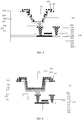
Fig. 3 is a structural schematic view of a pixel unit according to a second embodiment of the present invention; -
Fig. 4 is a structural schematic view of a pixel unit according to a third embodiment of the present invention; -
Fig. 5 is a structural schematic view of a pixel unit according to a fourth embodiment of the present invention; -
Fig. 6 is a structural schematic view of a pixel unit according to a fifth embodiment of the present invention; and -
Fig. 7 is a flow diagram of a method of manufacturing a pixel unit according to an eighth embodiment of the present invention. - In order to provide a more clear understanding of objects, technique solutions and advantages of embodiments of the present invention, the embodiments of the present invention will be further described hereinafter in detail and completely with reference to the attached drawings.
- A pixel unit used in a common low-temperature polycrystalline silicon thin film transistor organic light emitting diode (LTPS-TFT OLED) display apparatus is shown in
Fig. 1 . The pixel unit generally includes a low-temperature polycrystalline silicon thin film transistor served as athin film transistor 100 for driving, aplanarization layer 200, apixel definition layer 300, apixel electrode 400, alight emitting layer 500 and acommon electrode 600, and so on. Both side surfaces of thelight emitting layer 500 are contacted directly with thepixel definition layer 300. A light emitted by thelight emitting layer 500 scatters to the surroundings after passing through thepixel definition layer 300 and makes a color mixing with the lights scattered from other pixel units around this pixel unit, to seriously affect the display effect. Moreover, only a bottom surface of thelight emitting layer 500 gets in contact with thepixel electrode 400, accordingly, the luminous area is limited so that the overall luminance is adversely affected. In addition, in a technical process of manufacturing the pixel unit as shown inFig. 1 , generally, a polycrystalline silicon (Poly), a gate insulation layer (Gate 1), a gate (Gate 2), an interlayer deposition layer (ILD), a source and a drain (SD), a planarization layer (PLN), a pixel electrode (Anode), a pixel definition layer (PDL), a spacer layer (PS), a light emitting layer evaporation (EL) and a common electrode (Vcom) are manufactured in sequence. In this process, generally, two process steps are adopted successively to manufacture a through hole in theplanarization layer 200 and a through hole in thepixel definition layer 300. As a result, two masks are required, which is relatively complicated in process and relatively high in the cost. Moreover, in this process, the manner in which thepixel electrode 400 is firstly formed and then thepixel definition layer 300 is formed causes thepixel electrode 400 to be polluted by residual material for pixel electrode after thepixel definition layer 300 is formed, which adversely affects the luminous effect. Therefore, it is an urgent need in the art to provide a pixel unit which can avoid occurrence of the color mixing phenomenon and a method of manufacturing the pixel electrode which is simple in the process, and low in the cost, and has no influence on the luminous effect. - Referring to
Fig. 2, Fig. 2 shows a structural schematic view of a pixel unit according to a first embodiment of the present invention. The pixel unit is formed on a driver thin film transistor and includes: a planarization layer (PLN layer) 200, a pixel definition layer (PDL layer) 300, apixel electrode 400, alight emitting layer 500 and acommon electrode 600. - In this embodiment, the driver thin film transistor may be a low-temperature polycrystalline silicon thin film transistor which includes a
substrate 101, abuffer layer 102 formed on thesubstrate 101, anoutput electrode 103, achannel 104 and aninput electrode 105 formed on thebuffer layer 102, agate insulation layer 106 formed on thebuffer layer 102 as well as theoutput electrode 103, thechannel 104 and theinput electrode 105, acontrol terminal 107 formed on thegate insulation layer 106, and, an interlayer deposition layer 108 (ILD layer) formed on thecontrol terminal 107 and thegate insulation layer 106. A third throughhole 111 and a fourth throughhole 112 running through theinterlayer deposition layer 108 and thegate insulation layer 106 are formed directly above theoutput electrode 103 and theinput electrode 105, respectively. Anoutput terminal 109 has one end connected to theoutput electrode 103 and led out through the third throughhole 111, and the other end exposed on theinterlayer deposition layer 108, and, theinput terminal 110 has one end connected to theinput electrode 105 and led out through the fourth throughhole 112, and the other end exposed on theinterlayer deposition layer 108. - For the driver thin film transistor according to the present embodiment, if an N-type thin film transistor is adopted, the
control terminal 107 is embodied as a gate of the driver thin film transistor, theinput electrode 105 is embodied as a drain, theinput terminal 110 is embodied as a drain metal, theoutput electrode 103 is embodied as a source and theoutput terminal 109 is embodied as a source metal. If a P-type thin film transistor is adopted, thecontrol terminal 107 is embodied as a gate of the driver thin film transistor, theinput electrode 105 is embodied as a source, theinput terminal 110 is embodied as a source metal, theoutput electrode 103 is embodied as a drain and theoutput terminal 109 is embodied as a drain metal. - The
planarization layer 200 is formed on theinterlayer deposition layer 108, as well as on theoutput terminal 109 and theinput terminal 110, of the driver thin film transistor, and has a second throughhole 201 directly above theoutput terminal 109. Thepixel definition layer 300 is formed on theplanarization layer 200, and has a first throughhole 301 directly above the second throughhole 201. The first throughhole 301 has a greater size than the second throughhole 201, and is communicated with the second throughhole 201. - A
pixel electrode 400, alight emitting layer 500 and acommon electrode 600 are formed in sequence on thepixel definition layer 300. Thepixel electrode 400 comprises a bottom surface portion and a side surface portion. The bottom surface portion overspreads the bottom of the first throughhole 301 and is connected with theoutput terminal 109 through the second throughhole 201, and the side surface portion extends to a top of aside wall 302 of the first throughhole 301 on theside wall 302 of the first throughhole 301. Thelight emitting layer 500 is formed on thepixel electrode 400 and covers over thepixel electrode layer 400. Thecommon electrode 600 is formed on thelight emitting layer 500 and covers over thelight emitting layer 500 and extends on a top surface of thepixel definition layer 300. In addition, aspacer layer 700 is formed on thepixel definition layer 300. In the embodiments of the present invention, thepixel electrode 400 comprises a reflective electrode formed of indium tin oxide / silver / indium tin oxide (ITO/Ag/ITO) material, or of lightproof conductive material. In the pixel unit according to the embodiments of the present invention, thepixel electrode 400 is provided between thepixel definition layer 300 and thelight emitting layer 500, and a light emitted by thelight emitting layer 500 are partially reflected by the reflective electrode formed of indium tin oxide / silver / indium tin oxide (ITO/Ag/ITO) material, or are blocked by the lightproof conductive material, so that scattering of a light from thelight emitting layer 500 to the surroundings is greatly reduced, thereby greatly alleviating color mixing phenomenon occurred between the pixel units, to effectively solve the color mixing problem brought by scatting of the light. Thepixel electrode 400 includes the side surface portion, which enables area of thepixel electrode 400 to be increased, so that contact area between thepixel electrode 400 and thelight emitting layer 500 is increased, and accordingly luminous area of the pixel unit is increased without changing aperture ratio of the pixel unit, thereby enhancing overall luminance. - In an embodiment of the present invention, the
substrate 101 includes a glass material, thebuffer layer 102 includes silicon nitride (SiNx) or silicon dioxide (SiO2) or aluminum (Al) or aluminum oxide (AL2O3) material, theoutput electrode 103, thechannel 104 and theinput electrode 105 are polycrystalline silicon (P-Si) material, thegate insulation layer 106 includes silicon dioxide (SiO2) or bilayer material consisted of silicon dioxide (SiO2)/silicon nitride (SiNx) or TEOS material; thecontrol terminal 107 includes molybdenum niobium material, theoutput terminal 109 and theinput terminal 110 includes Ti-Al-Ti material, theinterlayer deposition layer 108 includes silicon nitride (SiNx) or silicon dioxide (SiO2) material, theplanarization layer 200 includes an organic film material, thepixel definition layer 300 includes polyimide (PI) material, thelight emitting layer 500 includes organic light emitting material such as Alq, Balq and DPVBi, etc., and, thecommon electrode 600 include metal alloy such as Mg-Ag. - In some embodiments, referring to
Fig. 2 , thepixel electrode 400 may further extend to the top surface of thepixel definition layer 300, and an end of thepixel electrode 400 is located on the top surface of thepixel definition layer 300. Anend 501 of the light emitting layer has a step shape and covers over the end of thepixel electrode 400. Anend 601 of the common electrode has a step shape and covers over theend 501 of the light emitting layer and extends on the top surface of thepixel definition layer 300. This further increases the areas of thepixel electrode 400 and thelight emitting layer 500, so that the contact area between thepixel electrode 400 and thelight emitting layer 500 is further increased, and accordingly, overall luminance of the pixel unit is further enhanced without changing aperture ratio of the pixel unit, while avoiding the color mixing problem caused by scattering of the light. -
Fig. 3 shows a structural schematic view of a pixel unit according to a second embodiment of the present invention. For brief purpose, technical features of the first embodiment which can be employed in the second embodiment are incorporated herein by reference, but are omitted to avoid duplicating description. The following description only relates to these technical features of the second embodiment different from the first embodiment. - The
side wall 302 of the first throughhole 301 in thepixel definition layer 300 has an outwardly cambered face, and the side surface of thepixel electrode 400 extends to the top of theside wall 302 of the first throughhole 301 on the outwardly cambered face of theside wall 302 of the first throughhole 301. Thelight emitting layer 500 is formed on thepixel electrode 400 and covers over thepixel definition layer 300. Thecommon electrode 600 is formed on thelight emitting layer 500 and covers over thelight emitting layer 500 and extends on the top surface of thepixel definition layer 300. The area of theside wall 302 of the first throughhole 301 in the pixel unit according to the second embodiment is greater than that of theside wall 302 of the first throughhole 301 in the pixel unit according to the first embodiment, which further increases the areas of thepixel electrode 400 and thelight emitting layer 500, so that the contact area between thepixel electrode 400 and thelight emitting layer 500 is further increased, and accordingly, overall luminance of the pixel unit is further enhanced without changing aperture ratio of the pixel unit, while avoiding the color mixing problem caused by scattering of the light. - In some embodiments, as shown in
Fig. 3 , thepixel electrode 400 may further extend to the top surface of thepixel definition layer 300, and an end of thepixel electrode 400 is located on the top surface of thepixel definition layer 300. Anend 501 of the light emitting layer has a step shape and covers over the end of thepixel electrode 400. Theend 601 of the common electrode has a step shape and covers over theend 501 of the light emitting layer and extends on the top surface of thepixel definition layer 300. This further increase the areas of thepixel electrode 400 and thelight emitting layer 500, so that the contact area between thepixel electrode 400 and thelight emitting layer 500 is further increased, and accordingly, overall luminance of the pixel unit is further enhanced without changing aperture ratio of the pixel unit, while avoiding the color mixing problem caused by scattering of the light. -
Fig. 4 shows a structural schematic view of a pixel unit according to a third embodiment of the present invention. For brief purpose, technical features of any one of the above embodiments which can be employed in the third embodiment are incorporated herein by reference, but are omitted to avoid duplicating description. The following description only relates to these technical features of the third embodiment different from other embodiments. - The
side wall 302 of the first throughhole 301 in thepixel definition layer 300 has an inwardly cambered face, and the side surface of thepixel electrode 400 extends to the top of theside wall 302 of the first throughhole 301 on the inwardly cambered face of theside wall 302 of the first throughhole 301. Thelight emitting layer 500 is formed on thepixel electrode 400 and covers over thepixel definition layer 300. Thecommon electrode 600 is formed on thelight emitting layer 500 and covers over thelight emitting layer 500 and extends on the top surface of thepixel definition layer 300. The area of theside wall 302 of the first throughhole 301 in the pixel unit according to the third embodiment is greater than that of theside wall 302 of the first throughhole 301 in the pixel unit according to the first embodiment, which further increases the areas of thepixel electrode 400 and thelight emitting layer 500, so that the contact area between thepixel electrode 400 and thelight emitting layer 500 is further increased, and accordingly, overall luminance of the pixel unit is further enhanced without changing aperture ratio of the pixel unit, while avoiding the color mixing problem caused by scattering of the light. - In some embodiments, as shown in
Fig. 4 , thepixel electrode 400 may further extend to the top surface of thepixel definition layer 300, and an end of thepixel electrode 400 is located on the top surface of thepixel definition layer 300. Anend 501 of the light emitting layer has a step shape and covers over the end of the pixel electrode. Theend 601 of the common electrode has a step shape and covers over theend 501 of the light emitting layer and extends on the top surface of thepixel definition layer 300. This further increase the areas of thepixel electrode 400 and thelight emitting layer 500, so that the contact area between thepixel electrode 400 and thelight emitting layer 500 is further increased, and accordingly, overall luminance of the pixel unit is further enhanced without changing aperture ratio of the pixel unit, while avoiding the color mixing problem caused by scattering of the light. -
Fig. 5 shows a structural schematic view of a pixel unit according to a fourth embodiment of the present invention. For brief purpose, technical features of any one of the above embodiments which can be employed in the fourth embodiment are incorporated herein by reference, but are omitted to avoid duplicating description. The following description only relates to these technical features of the fourth embodiment different from other embodiments. - An upper half portion of the first through
hole 301 in thepixel definition layer 300 is expanded outwardly to form a step, namely, theside wall 302 having a step shape is formed, and the side surface of thepixel electrode 400 extends to the top of theside wall 302 of the first throughhole 301 on the step-shapedside wall 302 of the first throughhole 301. Thelight emitting layer 500 is formed on thepixel electrode 400 and covers over thepixel definition layer 300. Thecommon electrode 600 is formed on thelight emitting layer 500 and covers over thelight emitting layer 500 and extends on the top surface of thepixel definition layer 300. The area of theside wall 302 of the first throughhole 301 in the pixel unit according to the fourth embodiment is greater than that of theside wall 302 of the first throughhole 301 in the pixel unit according to the first embodiment, which further increases the areas of thepixel electrode 400 and thelight emitting layer 500, so that the contact area between thepixel electrode 400 and thelight emitting layer 500 is further increased, and accordingly, overall luminance of the pixel unit is further enhanced, while avoiding the color mixing problem caused by scattering of the light. - In some embodiments, as shown in
Fig. 5 , thepixel electrode 400 may further extend to the top surface of thepixel definition layer 300, and an end of thepixel electrode 400 is located on the top surface of thepixel definition layer 300. Anend 501 of the light emitting layer has a step shape and covers over the end of the pixel electrode. Theend 601 of the common electrode has a step shape and covers over theend 501 of the light emitting layer and extends on the top surface of thepixel definition layer 300. This further increase the areas of thepixel electrode 400 and thelight emitting layer 500, so that the contact area between thepixel electrode 400 and thelight emitting layer 500 is further increased, and accordingly, overall luminance of the pixel unit is further enhanced, while avoiding the color mixing problem caused by scattering of the light. -
Fig. 6 shows a structural schematic view of a pixel unit according to a fifth embodiment of the present invention. For brief purpose, technical features of any one of the above embodiments which can be employed in the fifth embodiment are incorporated herein by reference, but are omitted to avoid duplicating description. The following description only relates to these technical features of the fifth embodiment different from other embodiments. - As another alternative embodiment of the present invention, the pixel unit further comprises: a
protective layer 800. Theprotective layer 800 is formed on thepixel definition layer 300 and covers over an end of thepixel electrode 400. Thelight emitting layer 500 is formed on the pixel electrode and covers over theprotective layer 800. Thecommon electrode 600 is formed on thelight emitting layer 500 and covers over thelight emitting layer 500 and extends on the top surface of thepixel definition layer 300. - The protective layer according to the present embodiment may be applied on the pixel unit according to any one of the abovementioned first to fourth embodiments of the present invention. The description will be followed by taking the pixel unit which is shown in
Fig. 1 and includes a protective layer as an example. Referring toFig. 6 , theprotective layer 800 covers over an end of thepixel electrode 400, to separate the end of thepixel electrode 400 and thecommon electrode 600 from each other, thereby preventing occurrence of point discharging phenomenon between thepixel electrode 400 and thecommon electrode 600 and enhancing display stability and display effect of the pixel unit. - An array substrate is provided according to a sixth embodiment of the present invention. The array substrate comprises a gate line, a data line and the pixel unit of any one of the abovementioned embodiments. The gate line is connected to the
control terminal 107 of the driver thin film transistor, and the data line is connected to theinput terminal 110 of the driver thin film transistor. - A display apparatus is provided according to a seventh embodiment of the present invention. The display apparatus comprises the array substrate of the sixth embodiment and a cover plate.
- A method of manufacturing a pixel unit is provided according to an eighth embodiment of the present invention. Referring to
Fig. 7 , the method is used for manufacturing the pixel unit of any one of the abovementioned first to fifth embodiments. The method may specifically comprise the following steps. - A
step 101 is of forming a planarization layer and a pixel definition layer in sequence on the driver thin film transistor, and forming, by a patterning process, a second through hole and a first through hole. - The mentioned patterning process may include but not be limited to Half Tone Mask process, as long as the second through hole and the first through hole are manufactured.
- When the Half Tone Mask process is adopted, the
step 101 specifically includes, coating an organic film material, and depositing polyimide (PI) material on the organic film material. Once a Half Tone Mask photolithographic process is adopted, one Half Tone Mask is used to form the second through hole in the planarization layer and the first through hole in the pixel definition layer at the same time. The Half Tone Mask is a multi-gray mask which is divided into a lightproof part, a semi-transparent part and a transparent part. The Half Tone Mask can be used to present three levels of exposures, namely an exposed part, a semi-exposed part and a non-exposed part, at one exposure process. In particular, in the Half Tone Mask, the transparent part is used for exposing for the second through hole and the semi-transparent part is used for exposing for the first through hole, so that the second through hole in the planarization layer and the first through hole in the pixel definition layer are formed at the same time. - In prior art, the second through hole and the first through hole are successively formed in two process steps, accordingly, two masks are required. When the Half Tone Mask process is adopted to form the second through hole and the first through hole, only one half tone mask is required, and the second through hole and the first through hole are formed in one photolithography process. This simplifies the process, shortens production time, cuts down the mask cost to significantly reduce the cost of the whole process, and improves productivity. The prior art manner in which the pixel electrode is firstly formed and then the pixel definition layer is formed causes the pixel electrode to be polluted by residual material for pixel electrode after the pixel definition layer is formed, which adversely affects the luminous effect. Whatever, the process, in which the pixel definition layer is formed firstly and then the pixel electrode is formed, provided by the present invention avoids the abovementioned problems and greatly enhances luminous effect.
- A
step 201 is of forming a pixel electrode. - The
step 201 may specifically include: forming an ITO coating, an Ag coating and an ITO coating in sequence. After being implemented with photolithography, wet-etching, photoresist removal and degradation, a pixel electrode is formed within the first through hole of the pixel definition layer. The pixel electrode has a bottom surface portion and a side surface portion, and the side surface portion extends to a top of a side wall of the first through hole on the side wall of the first through hole. - A
step 301 is of forming a spacer layer. - The
step 301 may specifically include: depositing polyimide (PI) material on the pixel definition layer, and forming the spacer layer after being implemented with photolithography. - In another embodiment of the present invention, the
step 301 may also specifically include: depositing polyimide (PI) material on the pixel definition layer, and forming, by one patterning process, the spacer layer and the protective layer which covers over the end of the pixel electrode. - In the
step 301 according to the present embodiment, the spacer layer and the protective layer may be synchronously manufactured in one deposition and one patterning process, which has no additional process step for formation of the protective layer, thereby simplifying the process and controlling the cost. - A
step 401 is of forming a light emitting layer and a common electrode. - The
step 401 may specifically include: - a sub-step 4011 of depositing, by a vacuum thermal evaporation process, an organic light emitting material, and forming, by a patterning process, a light emitting layer on the pixel electrode, the light emitting layer covering over the pixel electrode.
- In another embodiment of the present invention, the sub-step 4011 may also specifically include: depositing, by a vacuum thermal evaporation process, an organic light emitting material, and forming, by a patterning process, a light emitting layer on the pixel electrode, the light emitting layer covering over the pixel electrode and the protective layer.
- A sub-step 4012 is of: depositing, by a vacuum thermal evaporation process, a metal alloy, and forming, by a patterning process, a common electrode on the light emitting layer, the common electrode covering over the light emitting layer and extending on the top surface of the pixel definition layer.
- In some embodiments, before manufacturing the pixel unit, a step of manufacturing a driver thin film transistor, namely, a low-temperature polycrystalline silicon thin film transistors, is further included, and this step comprises the followings.
- A sub-step Oil is of forming a buffer layer and an active layer in sequence on the substrate.
- The sub-step 011 may specifically include:
- cleaning and pre-treating a glass substrate;
- forming the buffer layer on the glass substrate, then, forming the active layer made of a-Si material being implemented with hydrogen relief treatment; wherein, the buffer layer and the active layer are formed by using a plasma enhanced chemical vapor deposition (PECVD) process; and
- spin-cleaning the active layer, and implementing a polysilicon crystallization by using an excimer laser annealing (ELA) process, to generate polycrystalline silicon P-Si.
- A sub-step 012 is of etching the polycrystalline silicon to form an output electrode, an input electrode and a channel.
- The sub-step 012 may specifically include: etching the polycrystalline silicon P-Si by a photolithography process to form the output electrode and the input electrode and the channel which have been patterned.
- A sub-step 013 is of forming a gate insulation layer.
- The sub-step 013 may specifically include: implementing a spin clean firstly, depositing silicon dioxide (SiO2) or bi-layer material consisted of silicon dioxide (SiO2)/silicon nitride (SiNx) by using a plasma enhanced chemical vapor deposition (PECVD) process, and forming the gate insulation layer by a patterning process.
- A sub-step 014 is of forming a control terminal on the gate insulation layer.
- The sub-step 014 may specifically include: implementing a spin clean firstly, and implementing film deposition, photolithography, enhanced capacitively coupled plasma (ECCP) dry etching and photoresist removal on the molybdenum niobium material, to obtain the control terminal which has been patterned.
- A sub-step 015 is of forming an interlayer deposition layer and then etching a third through hole and a fourth through hole of the interlayer deposition layer and the gate insulation layer.
- The sub-step 015 may specifically include: implementing a clean with hydrofluoric acid (BHF), forming silicon nitride (SiNx) or silicon dioxide (SiO2) material into films and implementing hydrogenation, and then implementing photolithography, inductively coupled plasma (ICP) etching and photoresist removal, to obtain the third through hole and the fourth through hole.
- A sub-step 016 is of forming an output terminal and an input terminal.
- The sub-step 016 may specifically include: implementing a clean with hydrofluoric acid (BHF), forming Ti-Al-Ti material into a film, and then implementing photolithography, enhanced capacitively coupled plasma (ECCP) dry etching, photoresist removal and metal annealing, to obtain the output terminal and the input terminal.
- Thus it can be seen from the above, the pixel unit used in an organic light emitting diode display apparatus and the method of manufacturing the same, the array substrate and the display apparatus according to the embodiments of the present invention have at least one of the following beneficial advantages.
- (1) The side surface portion of the pixel electrode extends to the top of the first through hole on the side wall of the first through hole, which greatly reduces scattering of a light from the light emitting layer to the surroundings, so that color mixing phenomenon occurred between the pixel units are greatly alleviated, thereby effectively solving the color mixing problem brought by scatting of the light.
- (2) Area of the pixel electrode is increased, so that contact area between the pixel electrode and the light emitting layer is increased, and accordingly luminous area of the pixel unit is increased without changing aperture ratio of the pixel unit, thereby enhancing overall luminance.
- (3) Provision of the step-shaped ends of the light emitting layer and the common electrode further increase the luminous area, which also further enhances overall luminance.
- (4) Half Tone Mask is adopted in the manufacturing method to form the second through hole and the first through hole by one photolithographic process, which simplifies the process, shortens production time, cuts down the mask cost to significantly reduce the cost of the whole process, and improves productivity.
- (5) A manner in which the pixel definition layer is firstly formed and then the pixel electrode is formed avoids the pixel electrode to be polluted by residual material for pixel electrode after the pixel definition layer is formed, which improves the luminous effect.
- (6) The protective layer covers over an end of the pixel electrode, to separate the end of the pixel electrode and the common electrode from each other, thereby preventing occurrence of point discharging phenomenon between the pixel electrode and the common electrode and enhancing display stability and display effect of the pixel unit.
- To this, embodiments of the present invention have been described in conjunction with the drawings. In accordance with the above description, those skilled in the art may have a clear understanding of the pixel unit and the method of manufacturing the same, the array substrate and the display apparatus according to the present invention.
- It should be explained that, in the drawings or the description of the present disclosure, any implementations which are not illustrated or not described belong to well-knowledge for those skilled in the art and are not described and explained in detail. In addition, the abovementioned definitions of these elements are not only limited to these specific configuration, shape or manner disclosed in the embodiments, and those skilled in the art may easily make any simple change or replacement. The followings are taken as examples.
- (1) The side wall of the first through hole may also be presented in any other shape(s).
- (2) These orientational terminologies such as "above", "below", "front", "rear", "left", "right" and the likes are used for easing or simplifying the orientations in the drawings, instead of limiting the protective scope of the present invention.
- (3) Based on considerations in design and reliability, these abovementioned embodiments may be combined freely with one another or with other embodiments, that is, Technical features described in these embodiments may be combined freely to generate much more embodiments.
- The above specific embodiments are provided to further describe and explain objects, technique solutions and advantages of the present invention. It should be understood that, the above description is merely used to illustrate specific embodiments of the present invention, but not to limit the present invention. All of changes, equivalent alternatives, modifications, made within principles and spirit of the present invention, should be included within the scope of the present invention.
Claims (10)
- A pixel unit, characterized by comprising: a pixel definition layer, a pixel electrode, a light emitting layer and a common electrode; wherein,
the pixel definition layer has a firs through hole, within which the pixel electrode, the light emitting layer and the common electrode are laminated;
the pixel electrode comprises a bottom surface portion and a side surface portion, the side surface portion extending to a top of a side wall of the first through hole on the side wall of the first through hole;
the light emitting layer is formed on the pixel electrode and covers over the pixel electrode; and
the common electrode is formed on the light emitting layer, covers over the light emitting layer and extends on a top surface of the pixel definition layer. - The pixel unit of claim 1, characterized in that, the side wall of the first through hole in the pixel definition layer is formed as a flat face, an outwardly cambered face, or an inwardly cambered face or in a step shape.
- The pixel unit of claim 1, characterized in that, the pixel electrode extends to the top surface of the pixel definition layer, an end of the pixel electrode is on the top surface of the pixel definition layer, and, both an end of the light emitting layer and an end of the common electrode have a step shape.
- The pixel unit of claim 1, characterized by further comprising: a protective layer formed on the pixel definition layer and covering over an end of the pixel electrode, wherein the light emitting layer covers over the protective layer.
- The pixel unit of claim 1, characterized by further comprising: a planarization layer having a second through hole at a location corresponding to an output terminal of a driver thin film transistor, wherein the pixel definition layer is formed on the planarization layer, and the first through hole is located directly above the second through hole and is communicated with the second through hole.
- An array substrate, characterized by comprising: the pixel unit of any one of claims 1-5.
- A display apparatus, characterized by comprising: the array substrate of claim 6.
- A method of manufacturing a pixel unit, characterized in that, the method is used for manufacturing the pixel unit of claim 1, and comprises:forming a pixel definition layer and forming a first through hole in the pixel definition layer;forming a pixel electrode within the first through hole of the pixel definition layer, the pixel electrode having a bottom surface and a side surface, and the side surface extending to a top of a side wall of the first through hole on the side wall of the first through hole;forming a light emitting layer that covers over the pixel electrode; andforming a common electrode that covers over the light emitting layer and extends on a top surface of the pixel definition layer.
- The method of claim 8, characterized in that, the forming the pixel definition layer and the forming the first through hole in the pixel definition layer, comprises:depositing two layers of organic material in sequence, and forming, by one patterning process, a second through hole in the planarization layer and the first through hole in the pixel definition layer.
- The method of claim 8, characterized in that, after the forming the pixel electrode within the first through hole of the pixel definition layer and before the forming the light emitting layer that covers over the pixel electrode, the method further comprises:depositing an organic material on the pixel definition layer, and, forming, by one patterning process, a spacer layer and a protective layer that covers over an end of the pixel electrode; andthe forming the light emitting layer that covers over the pixel electrode further comprises: forming the light emitting layer on the pixel electrode such that the light emitting layer covers over the pixel electrode and the protective layer.
Applications Claiming Priority (2)
| Application Number | Priority Date | Filing Date | Title |
|---|---|---|---|
| CN201610364630.6A CN105810719B (en) | 2016-05-27 | 2016-05-27 | A kind of pixel unit and preparation method thereof, array substrate and display device |
| PCT/CN2017/070258 WO2017202035A1 (en) | 2016-05-27 | 2017-01-05 | Pixel unit and method for preparing the same, array substrate and display device |
Publications (2)
| Publication Number | Publication Date |
|---|---|
| EP3282483A1 true EP3282483A1 (en) | 2018-02-14 |
| EP3282483A4 EP3282483A4 (en) | 2018-10-24 |
Family
ID=56452133
Family Applications (1)
| Application Number | Title | Priority Date | Filing Date |
|---|---|---|---|
| EP17737196.0A Withdrawn EP3282483A4 (en) | 2016-05-27 | 2017-01-05 | Pixel unit and method for preparing the same, array substrate and display device |
Country Status (4)
| Country | Link |
|---|---|
| US (1) | US20180158886A1 (en) |
| EP (1) | EP3282483A4 (en) |
| CN (1) | CN105810719B (en) |
| WO (1) | WO2017202035A1 (en) |
Cited By (1)
| Publication number | Priority date | Publication date | Assignee | Title |
|---|---|---|---|---|
| CN116261923A (en) * | 2020-07-16 | 2023-06-13 | 应用材料公司 | Hierarchical Bevel Reflective Structures for OLED Display Pixels |
Families Citing this family (18)
| Publication number | Priority date | Publication date | Assignee | Title |
|---|---|---|---|---|
| CN105810719B (en) * | 2016-05-27 | 2019-08-06 | 京东方科技集团股份有限公司 | A kind of pixel unit and preparation method thereof, array substrate and display device |
| CN108878472B (en) * | 2017-05-12 | 2021-04-06 | 京东方科技集团股份有限公司 | An OLED display substrate and its manufacturing method, and a display device |
| KR102606282B1 (en) * | 2017-06-19 | 2023-11-27 | 삼성디스플레이 주식회사 | Display device |
| CN108565357B (en) * | 2018-01-09 | 2020-06-30 | 深圳市华星光电半导体显示技术有限公司 | OLED display panel for ink-jet printing and preparation method thereof |
| DE112019001693T5 (en) * | 2018-03-30 | 2020-12-10 | Sony Semiconductor Solutions Corporation | DISPLAY DEVICE, METHOD OF MANUFACTURING A DISPLAY DEVICE, AND ELECTRONIC DEVICE |
| CN110571358B (en) * | 2018-06-05 | 2022-07-19 | 中芯国际集成电路制造(上海)有限公司 | Semiconductor device and method for manufacturing the same |
| KR102671037B1 (en) * | 2018-11-07 | 2024-06-03 | 삼성디스플레이 주식회사 | Organic light emitting display apparatus and method of manufacturing the same |
| US11158836B2 (en) * | 2019-03-19 | 2021-10-26 | Innolux Corporation | Light emitting device |
| KR102894202B1 (en) * | 2019-08-19 | 2025-12-02 | 삼성디스플레이 주식회사 | Organic light emitting diode display device and manufacturing method thereof |
| CN111029371A (en) * | 2019-11-01 | 2020-04-17 | 武汉华星光电半导体显示技术有限公司 | Organic light emitting diode display panel, display device and manufacturing method |
| CN111081737A (en) * | 2019-12-05 | 2020-04-28 | 深圳市华星光电半导体显示技术有限公司 | Method for preparing an array substrate and array substrate |
| CN112420783B (en) * | 2020-11-04 | 2022-09-09 | 武汉华星光电半导体显示技术有限公司 | Display panel and electronic device |
| CN114639793A (en) * | 2020-12-16 | 2022-06-17 | 京东方科技集团股份有限公司 | Display substrate, preparation method thereof and display device |
| CN112885885A (en) * | 2021-02-01 | 2021-06-01 | 武汉华星光电半导体显示技术有限公司 | Display panel, display device and manufacturing method of display panel |
| CN113066829A (en) | 2021-03-11 | 2021-07-02 | 重庆京东方显示技术有限公司 | Display panel, preparation method thereof and display device |
| CN113629205B (en) * | 2021-07-19 | 2023-02-10 | 武汉华星光电半导体显示技术有限公司 | Display panel and display device |
| WO2025027844A1 (en) * | 2023-08-03 | 2025-02-06 | シャープディスプレイテクノロジー株式会社 | Light-emitting element, method for manufacturing same, and display device equipped with same |
| WO2025041314A1 (en) * | 2023-08-23 | 2025-02-27 | シャープディスプレイテクノロジー株式会社 | Light emission device, display device, and method for producing light emission device |
Family Cites Families (13)
| Publication number | Priority date | Publication date | Assignee | Title |
|---|---|---|---|---|
| JP2000260571A (en) * | 1999-03-11 | 2000-09-22 | Sanyo Electric Co Ltd | Electroluminescence display device |
| JP3702858B2 (en) * | 2001-04-16 | 2005-10-05 | セイコーエプソン株式会社 | Electro-optical device and electronic apparatus |
| US7227306B2 (en) * | 2003-08-28 | 2007-06-05 | Samsung Sdi Co., Ltd. | Organic electroluminescence display having recessed electrode structure |
| KR101600816B1 (en) * | 2008-11-14 | 2016-03-09 | 삼성디스플레이 주식회사 | Organic Light Emitting Diode Display and Manufacturing Method thereof |
| KR20130044118A (en) * | 2010-08-06 | 2013-05-02 | 파나소닉 주식회사 | Organic el display panel, display device, and method of manufacturing organic el display panel |
| KR102021027B1 (en) * | 2013-02-28 | 2019-09-16 | 삼성디스플레이 주식회사 | Organic luminescence emitting display device |
| US9224980B2 (en) * | 2013-03-28 | 2015-12-29 | Semiconductor Energy Laboratory Co., Ltd. | Light-emitting device |
| KR102064392B1 (en) * | 2013-06-04 | 2020-01-10 | 삼성디스플레이 주식회사 | Organic luminescence emitting display device and method for manufacturing the same |
| KR102036328B1 (en) * | 2013-06-07 | 2019-10-25 | 삼성디스플레이 주식회사 | Organic luminescence emitting display device and method for manufacturing the same |
| CN104282844B (en) * | 2013-07-08 | 2017-02-08 | 上海和辉光电有限公司 | Organic light-emitting structure, manufacturing method thereof, and organic light-emitting component |
| KR102285384B1 (en) * | 2014-09-15 | 2021-08-04 | 삼성디스플레이 주식회사 | Thin film transistor array substrate and manufacturing method for the same and display |
| KR20160080994A (en) * | 2014-12-30 | 2016-07-08 | 삼성디스플레이 주식회사 | Organic luminescence emitting display device and method for manufacturing the same |
| CN105810719B (en) * | 2016-05-27 | 2019-08-06 | 京东方科技集团股份有限公司 | A kind of pixel unit and preparation method thereof, array substrate and display device |
-
2016
- 2016-05-27 CN CN201610364630.6A patent/CN105810719B/en active Active
-
2017
- 2017-01-05 WO PCT/CN2017/070258 patent/WO2017202035A1/en not_active Ceased
- 2017-01-05 EP EP17737196.0A patent/EP3282483A4/en not_active Withdrawn
- 2017-01-05 US US15/544,666 patent/US20180158886A1/en not_active Abandoned
Cited By (3)
| Publication number | Priority date | Publication date | Assignee | Title |
|---|---|---|---|---|
| CN116261923A (en) * | 2020-07-16 | 2023-06-13 | 应用材料公司 | Hierarchical Bevel Reflective Structures for OLED Display Pixels |
| JP2023534450A (en) * | 2020-07-16 | 2023-08-09 | アプライド マテリアルズ インコーポレイテッド | Inclined Gradient Reflective Structures for OLED Display Pixels |
| EP4182981A4 (en) * | 2020-07-16 | 2024-05-22 | Applied Materials, Inc. | Graded slope reflective structures for oled display pixels |
Also Published As
| Publication number | Publication date |
|---|---|
| CN105810719B (en) | 2019-08-06 |
| CN105810719A (en) | 2016-07-27 |
| US20180158886A1 (en) | 2018-06-07 |
| WO2017202035A1 (en) | 2017-11-30 |
| EP3282483A4 (en) | 2018-10-24 |
Similar Documents
| Publication | Publication Date | Title |
|---|---|---|
| US20180158886A1 (en) | Pixel Unit And Method Of Manufacturing The Same, And Array Substrate And Display Apparatus | |
| CN107958916B (en) | display device | |
| US10002847B2 (en) | OLED pixel unit, transparent display device, method for fabricating the same, display apparatus | |
| JP5060738B2 (en) | Image display device | |
| US11665936B2 (en) | OLED display panel and manufacturing method thereof | |
| JP6460582B2 (en) | Manufacturing method of AMOLED back panel | |
| US8946008B2 (en) | Organic light emitting diode display, thin film transitor array panel, and method of manufacturing the same | |
| US20170194416A1 (en) | Array substrate, method for manufacturing the same and display device | |
| CN103531607B (en) | Organic light emitting display panel and its manufacturing method | |
| KR102124827B1 (en) | Display Panel having Process Key therein | |
| KR102078022B1 (en) | Dual sided emission type Organic electro luminescent device | |
| US10355138B2 (en) | LTPS TFT substrate and method for manufacturing the same | |
| WO2014117512A1 (en) | Method for preparing thin film transistor, method for preparing thin film transistor driving back panel, and thin film transistor driving back panel | |
| US20190027612A1 (en) | Thin-film transistor and manufacturing method thereof, array substrate, and display apparatus | |
| KR20150067974A (en) | Organic electro luminescent device and method of fabricating the same | |
| CN110112142A (en) | Array substrate and its manufacturing method, display panel and electronic device | |
| KR100635065B1 (en) | Organic EL display device and manufacturing method thereof | |
| TWI458089B (en) | Display device and method of manufacturing the same | |
| US9117781B2 (en) | Organic light emitting diode display and method for manufacturing the same | |
| KR20140083150A (en) | Organic electro luminescent device and method of fabricating the same | |
| KR20150033406A (en) | Organic electro-luminescent device and methode of fabricating the same | |
| KR102092544B1 (en) | Array substrate for liquid crystal display device and method of fabricating the same | |
| KR20120053770A (en) | Method for fabricating array substrate having thin film transistor | |
| TWI459566B (en) | Thin film transistor, display device therewith and method of manufacturing thin film transistor and display device | |
| US20250081757A1 (en) | Display device and method of manufacturing the same |
Legal Events
| Date | Code | Title | Description |
|---|---|---|---|
| STAA | Information on the status of an ep patent application or granted ep patent |
Free format text: STATUS: UNKNOWN |
|
| STAA | Information on the status of an ep patent application or granted ep patent |
Free format text: STATUS: THE INTERNATIONAL PUBLICATION HAS BEEN MADE |
|
| PUAI | Public reference made under article 153(3) epc to a published international application that has entered the european phase |
Free format text: ORIGINAL CODE: 0009012 |
|
| STAA | Information on the status of an ep patent application or granted ep patent |
Free format text: STATUS: REQUEST FOR EXAMINATION WAS MADE |
|
| 17P | Request for examination filed |
Effective date: 20170719 |
|
| AK | Designated contracting states |
Kind code of ref document: A1 Designated state(s): AL AT BE BG CH CY CZ DE DK EE ES FI FR GB GR HR HU IE IS IT LI LT LU LV MC MK MT NL NO PL PT RO RS SE SI SK SM TR |
|
| AX | Request for extension of the european patent |
Extension state: BA ME |
|
| A4 | Supplementary search report drawn up and despatched |
Effective date: 20180925 |
|
| RIC1 | Information provided on ipc code assigned before grant |
Ipc: H01L 51/52 20060101ALI20180919BHEP Ipc: H01L 27/32 20060101AFI20180919BHEP |
|
| DAV | Request for validation of the european patent (deleted) | ||
| DAX | Request for extension of the european patent (deleted) | ||
| STAA | Information on the status of an ep patent application or granted ep patent |
Free format text: STATUS: EXAMINATION IS IN PROGRESS |
|
| 17Q | First examination report despatched |
Effective date: 20210325 |
|
| STAA | Information on the status of an ep patent application or granted ep patent |
Free format text: STATUS: THE APPLICATION IS DEEMED TO BE WITHDRAWN |
|
| 18D | Application deemed to be withdrawn |
Effective date: 20210805 |