EP3279928A1 - Method for producing bonded body - Google Patents
Method for producing bonded body Download PDFInfo
- Publication number
- EP3279928A1 EP3279928A1 EP15879271.3A EP15879271A EP3279928A1 EP 3279928 A1 EP3279928 A1 EP 3279928A1 EP 15879271 A EP15879271 A EP 15879271A EP 3279928 A1 EP3279928 A1 EP 3279928A1
- Authority
- EP
- European Patent Office
- Prior art keywords
- assembled body
- heating plate
- pressure
- bonded
- manufacturing
- Prior art date
- Legal status (The legal status is an assumption and is not a legal conclusion. Google has not performed a legal analysis and makes no representation as to the accuracy of the status listed.)
- Withdrawn
Links
Images








Classifications
-
- H—ELECTRICITY
- H10—SEMICONDUCTOR DEVICES; ELECTRIC SOLID-STATE DEVICES NOT OTHERWISE PROVIDED FOR
- H10W—GENERIC PACKAGES, INTERCONNECTIONS, CONNECTORS OR OTHER CONSTRUCTIONAL DETAILS OF DEVICES COVERED BY CLASS H10
- H10W72/00—Interconnections or connectors in packages
- H10W72/071—Connecting or disconnecting
- H10W72/073—Connecting or disconnecting of die-attach connectors
-
- H—ELECTRICITY
- H10—SEMICONDUCTOR DEVICES; ELECTRIC SOLID-STATE DEVICES NOT OTHERWISE PROVIDED FOR
- H10W—GENERIC PACKAGES, INTERCONNECTIONS, CONNECTORS OR OTHER CONSTRUCTIONAL DETAILS OF DEVICES COVERED BY CLASS H10
- H10W72/00—Interconnections or connectors in packages
- H10W72/071—Connecting or disconnecting
-
- H—ELECTRICITY
- H10—SEMICONDUCTOR DEVICES; ELECTRIC SOLID-STATE DEVICES NOT OTHERWISE PROVIDED FOR
- H10W—GENERIC PACKAGES, INTERCONNECTIONS, CONNECTORS OR OTHER CONSTRUCTIONAL DETAILS OF DEVICES COVERED BY CLASS H10
- H10W72/00—Interconnections or connectors in packages
- H10W72/071—Connecting or disconnecting
- H10W72/0711—Apparatus therefor
- H10W72/07141—Means for applying energy, e.g. ovens or lasers
-
- H—ELECTRICITY
- H10—SEMICONDUCTOR DEVICES; ELECTRIC SOLID-STATE DEVICES NOT OTHERWISE PROVIDED FOR
- H10W—GENERIC PACKAGES, INTERCONNECTIONS, CONNECTORS OR OTHER CONSTRUCTIONAL DETAILS OF DEVICES COVERED BY CLASS H10
- H10W72/00—Interconnections or connectors in packages
- H10W72/071—Connecting or disconnecting
- H10W72/0711—Apparatus therefor
- H10W72/07173—Means for moving chips, wafers or other parts, e.g. conveyor belts
-
- H—ELECTRICITY
- H10—SEMICONDUCTOR DEVICES; ELECTRIC SOLID-STATE DEVICES NOT OTHERWISE PROVIDED FOR
- H10W—GENERIC PACKAGES, INTERCONNECTIONS, CONNECTORS OR OTHER CONSTRUCTIONAL DETAILS OF DEVICES COVERED BY CLASS H10
- H10W72/00—Interconnections or connectors in packages
- H10W72/071—Connecting or disconnecting
- H10W72/0711—Apparatus therefor
- H10W72/07178—Means for aligning
-
- H—ELECTRICITY
- H10—SEMICONDUCTOR DEVICES; ELECTRIC SOLID-STATE DEVICES NOT OTHERWISE PROVIDED FOR
- H10W—GENERIC PACKAGES, INTERCONNECTIONS, CONNECTORS OR OTHER CONSTRUCTIONAL DETAILS OF DEVICES COVERED BY CLASS H10
- H10W72/00—Interconnections or connectors in packages
- H10W72/071—Connecting or disconnecting
- H10W72/073—Connecting or disconnecting of die-attach connectors
- H10W72/07331—Connecting techniques
-
- H—ELECTRICITY
- H10—SEMICONDUCTOR DEVICES; ELECTRIC SOLID-STATE DEVICES NOT OTHERWISE PROVIDED FOR
- H10W—GENERIC PACKAGES, INTERCONNECTIONS, CONNECTORS OR OTHER CONSTRUCTIONAL DETAILS OF DEVICES COVERED BY CLASS H10
- H10W72/00—Interconnections or connectors in packages
- H10W72/071—Connecting or disconnecting
- H10W72/073—Connecting or disconnecting of die-attach connectors
- H10W72/07331—Connecting techniques
- H10W72/07332—Compression bonding, e.g. thermocompression bonding
-
- H—ELECTRICITY
- H10—SEMICONDUCTOR DEVICES; ELECTRIC SOLID-STATE DEVICES NOT OTHERWISE PROVIDED FOR
- H10W—GENERIC PACKAGES, INTERCONNECTIONS, CONNECTORS OR OTHER CONSTRUCTIONAL DETAILS OF DEVICES COVERED BY CLASS H10
- H10W72/00—Interconnections or connectors in packages
- H10W72/30—Die-attach connectors
- H10W72/321—Structures or relative sizes of die-attach connectors
- H10W72/325—Die-attach connectors having a filler embedded in a matrix
-
- H—ELECTRICITY
- H10—SEMICONDUCTOR DEVICES; ELECTRIC SOLID-STATE DEVICES NOT OTHERWISE PROVIDED FOR
- H10W—GENERIC PACKAGES, INTERCONNECTIONS, CONNECTORS OR OTHER CONSTRUCTIONAL DETAILS OF DEVICES COVERED BY CLASS H10
- H10W72/00—Interconnections or connectors in packages
- H10W72/30—Die-attach connectors
- H10W72/351—Materials of die-attach connectors
- H10W72/352—Materials of die-attach connectors comprising metals or metalloids, e.g. solders
-
- H—ELECTRICITY
- H10—SEMICONDUCTOR DEVICES; ELECTRIC SOLID-STATE DEVICES NOT OTHERWISE PROVIDED FOR
- H10W—GENERIC PACKAGES, INTERCONNECTIONS, CONNECTORS OR OTHER CONSTRUCTIONAL DETAILS OF DEVICES COVERED BY CLASS H10
- H10W72/00—Interconnections or connectors in packages
- H10W72/30—Die-attach connectors
- H10W72/351—Materials of die-attach connectors
- H10W72/353—Materials of die-attach connectors not comprising solid metals or solid metalloids, e.g. ceramics
-
- H—ELECTRICITY
- H10—SEMICONDUCTOR DEVICES; ELECTRIC SOLID-STATE DEVICES NOT OTHERWISE PROVIDED FOR
- H10W—GENERIC PACKAGES, INTERCONNECTIONS, CONNECTORS OR OTHER CONSTRUCTIONAL DETAILS OF DEVICES COVERED BY CLASS H10
- H10W90/00—Package configurations
- H10W90/701—Package configurations characterised by the relative positions of pads or connectors relative to package parts
- H10W90/731—Package configurations characterised by the relative positions of pads or connectors relative to package parts of die-attach connectors
- H10W90/734—Package configurations characterised by the relative positions of pads or connectors relative to package parts of die-attach connectors between a chip and a stacked insulating package substrate, interposer or RDL
-
- H—ELECTRICITY
- H10—SEMICONDUCTOR DEVICES; ELECTRIC SOLID-STATE DEVICES NOT OTHERWISE PROVIDED FOR
- H10W—GENERIC PACKAGES, INTERCONNECTIONS, CONNECTORS OR OTHER CONSTRUCTIONAL DETAILS OF DEVICES COVERED BY CLASS H10
- H10W90/00—Package configurations
- H10W90/701—Package configurations characterised by the relative positions of pads or connectors relative to package parts
- H10W90/731—Package configurations characterised by the relative positions of pads or connectors relative to package parts of die-attach connectors
- H10W90/736—Package configurations characterised by the relative positions of pads or connectors relative to package parts of die-attach connectors between a chip and a stacked lead frame, conducting package substrate or heat sink
Definitions
- the present invention relates to a method of manufacturing a bonded body.
- the metal particle paste is a conductive paste of a low-temperature baking type which contains nano-sized or submicron-sized metal particles in a solvent, and makes use of a low-temperature sintering phenomenon and high surface activity of the metal particles.
- the above-mentioned semiconductor device can be manufactured by a following bonding step.
- An assembled body 10 where a semiconductor element 14 is mounted on a substrate 12 on which a conductor pattern is formed with a metal particle paste 16 interposed therebetween (see Fig. 18A ) is placed on an upper surface of a first heating plate 920 on a lower side out of two heating plates (first heating plate 920 and second heating plate 922) (see Fig. 18B ).
- the second heating plate 922 on an upper side is descended toward the first heating plate 920 thus heating the above-mentioned assembled body 10 while applying pressure to the assembled body 10 whereby the substrate 12 on which the conductor pattern is formed and the semiconductor element 14 are bonded to each other (see Fig. 18C and Fig. 18D ).
- Patent Literature 1 JP-A-2012-9703
- Such a problem is not a problem which occurs only in manufacturing a semiconductor device having the structure where a substrate on which a conductor pattern is formed and a semiconductor element are bonded to each other using a metal particle paste, and is also a problem which is likely to occur in bonded bodies in general having the structure where "a substrate on which a conductor pattern is formed or another substrate” and "a semiconductor element or another electronic part" are bonded to each other using a metal particle paste.
- the present invention has been made to overcome the above-mentioned drawbacks, and it is an object of the present invention to provide a method of manufacturing a bonded body capable of bonding a substrate and an electronic part with a bonding strength higher than a bonding strength used in the prior art.
- the bonding step is performed under a condition that a temperature of the assembled body at the time of starting applying of pressure to the assembled body (that is, at the time of starting the applying of pressure of the assembled body) by two heating plates falls within a range of from 0°C to 150°C. Accordingly, in the bonding step, a sintering reaction (solidifying reaction) minimally occurs in a metal particle paste before pressure is applied to the assembled body. As a result, a substrate and an electronic part can be bonded to each other with a bonding strength higher than that of the prior art.
- the reason that the bonding step is performed under a condition that a temperature of the assembled body at the time of starting the applying of pressure is 150°C or below is as follows. That is, when the bonding step is performed under a condition that a temperature of the assembled body at the time of starting the applying of pressure is higher than 150°C, a sintering reaction is liable to occur in a metal particle paste before pressure is applied to the assembled body. As a result, there may be a case where bonding between a substrate and an electronic part with a bonding strength higher than that of the prior art becomes difficult.
- the reason that the bonding step is performed under a condition that a temperature of the assembled body at the time of starting the applying of pressure becomes 0°C or above is as follows. That is, when the bonding step is performed under a condition that a temperature of the assembled body at the time of starting the applying of pressure is lower than 0°C, it takes a long time until the assembled body is heated to a temperature which enables bonding. As a result, it takes a long time for bonding a substrate and an electronic part to each other thus giving rise to a case where productivity at the time of performing a bonding step is lowered.
- a method of manufacturing a bonded body according to an embodiment 1 is a method of manufacturing a bonded body for manufacturing a bonded body 11 (semiconductor device) having the structure where a substrate 12 (a substrate on which a conductor pattern is formed) and an electronic part 14 (semiconductor element) are bonded to each other with a metal particle paste 16 interposed therebetween (a method of manufacturing a semiconductor device).
- the substrate 12, the electronic part 14, and the metal particle paste 16 are explained in detail.
- substrate means a part on which an electronic part is mounted.
- the substrate 12 mounts the electronic part 14 thereon.
- the substrate 12 of the embodiment 1 is, for example, a printed circuit board where a conductor pattern is formed on a body made of a non-conductive material.
- a material for forming the substrate 12 a material which has resistance to a sintering temperature of a metal particle paste 16 (for example, 300°C although the sintering temperature depends on a kind of material) can be used.
- a resin or a ceramic having heat resistance is used for forming the body, and metal is used for forming the conductor pattern.
- the substrate to which the present invention is applicable may be a DCB (Direct Copper Bond) substrate or a lead frame. Further, it is sufficient that the substrate to which the present invention is applicable is a substrate on which an electronic part can be mounted.
- the substrate may be a silicon chip. That is, the present invention is also applicable to the connection between a silicon chip and a conductive connector.
- electronic part means a part which is used in an electric product and is particularly required to be electrically connected to the substrate.
- the electronic part 14 is a semiconductor element, for example.
- the electronic part 14 besides the above-mentioned semiconductor element (for example, a semiconductor chip on which an integrated circuit is mounted), an electric motor, a resistor, a capacitor, a piezoelectric element, a connector, a switch, an antenna, and a conductive connector can be exemplified.
- the method of manufacturing a bonded body of the present invention is particularly preferably applicable to a case where a bonded body formed by bonding at least one semiconductor element and a substrate to each other, that is, a semiconductor device is manufactured.
- the number of electronic parts 14 used in the embodiment 1 is one, the present invention is also applicable to the case where two or more electronic parts are used. When two or more electronic parts are used, the electronic parts may be formed of one kind of electronic part, or may be formed of plural kinds of electronic parts.
- the metal particle paste 16 is a low-temperature baking-type conductive paste which makes use of low-temperature sintering phenomenon brought about by a quantum size effect of metal particles and high surface activity of the metal particles .
- the metal particle paste 16 contains metal particles, an organic dispersion material, an organic dispersion material capturing material, and a volatile organic solvent, for example.
- metal particles formed of metal nanoparticles for example, metal particles having an average diameter of approximately 100nm or less
- metal particles formed of metal submicron particles for example, metal particles having an average diameter which falls within a range of from approximately 0. 1 ⁇ m to approximately 1 ⁇ m
- metal particles formed of both the metal nanoparticles and the metal submicron particles can be used.
- the organic dispersion material covers surfaces of metal particles at a room temperature, and performs a function of holding metal particles in an independently dispersed state.
- the organic dispersion material capturing material reacts with the organic dispersion material which covers metal particles at a high temperature and performs a function of removing the organic dispersion material from a surface of the metal particle.
- the volatile organic solvent has a function of capturing a chemical reaction product formed between the organic dispersion material and the organic dispersion material capturing material and also performs a function of releasing the chemical reaction product to the outside of a system in the form of a gas.
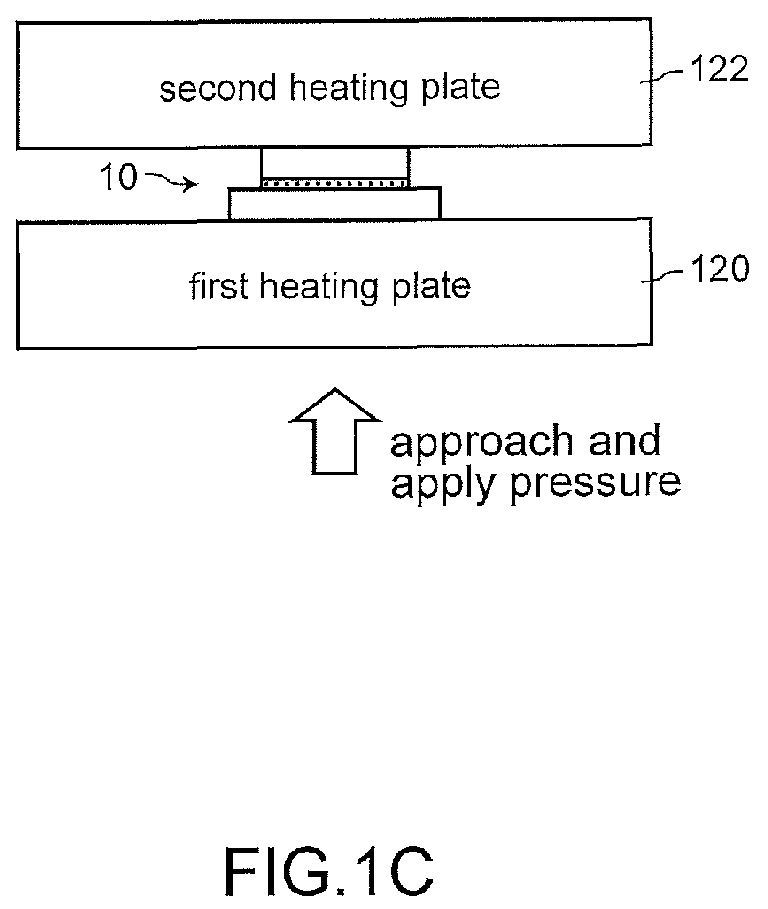
- the method of manufacturing a bonded body according to the embodiment 1 includes: an assembled body forming step of forming an assembled body 10 where the electronic part 14 is mounted on the substrate 12 with the metal particle paste 16 interposed therebetween (see Fig. 1A ); an assembled body arranging step of arranging the assembled body 10 between two heating plates (a first heating plate 120, a second heating plate 122) arranged in an opposedly facing manner (see Fig. 1B ); and a bonding step of bonding the substrate 12 and the electronic part 14 to each other by heating while applying pressure to the assembled body 10 by moving at least one (the first heating plate 120) of two heating plates (the first heating plate 120, the second heating plate 122) to the other (the second heating plate 122) of two heating plates (see Fig. 1C).
- Fig. 1D shows a state where two heating plates (the first heating plate 120, the second heating plate 122) are separated from each other by lowering the first heating plate 120 after the bonding step is finished, and a bonded body 11 can be taken out to the outside.
- the assembled body 10 is arranged in a space defined between two heating plates (the first heating plate 120, the second heating plate 122) at a position where the assembled body 10 is in contact with neither one of two heating plates (the first heating plate 120, the second heating plate 122) (see Fig. 1B ) and hence, the bonding step is performed under a condition that a temperature T 1 (a first temperature T 1 ) of the assembled body at the time of starting applying of the pressure to the assembled body 10 (that is, at the time of starting the applying of pressure) by two heating plates (the first heating plate 120, the second heating plate 122) falls within a range of from 0°C to 150°C (see Fig. 2 ).
- a specific method of arranging the assembled body 10 in a space defined between two heating plates (the first heating plate 120, and the second heating plate 122) at a position where the assembled body 10 is in contact with neither one of two heating plates (the first heating plate 120, the second heating plate 122) in the assembled body arranging step is described later (see Fig. 3 and Fig. 4 described later).
- the assembled body 10 is arranged in a space defined between two heating plates (the first heating plate 120, the second heating plate 122) at a position where the assembled body 10 is in contact with neither one of two heating plates (the first heating plate 120, the second heating plate 122) (see Fig. 1B ).
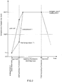
- the bonding step is performed under a condition that a temperature T1 of the assembled body at the time of starting applying of pressure to the assembled body 10 (that is, at the time of starting the applying of pressure) by two heating plates (the first heating plate 120, the second heating plate 122) falls within a range of from 0°C to 150°C (see a curve of the embodiment 1 shown in Fig. 2 ).
- a sintering reaction minimally occurs in a metal particle paste before pressure is applied to the assembled body.
- a substrate and an electronic part can be bonded to each other with a bonding strength higher than that of the prior art.
- the reason that the bonding step is performed under a condition that a temperature T 1 of the assembled body at the time of starting the applying of pressure is 150°C or below is as follows. That is, when the bonding step is performed under a condition that a temperature T 1 of the assembled body at the time of starting the applying of pressure is higher than 150°C (see a curve of the prior art shown in Fig. 2 ), a sintering reaction is liable to occur in a metal particle paste before pressure is applied to the assembled body. As a result, there may be a case where bonding between a substrate and an electronic part with a bonding strength higher than that of the prior art becomes difficult.
- a temperature T1 of the assembled body at the time of starting the applying of pressure is 135°C or below
- a temperature T 1 of the assembled body at the time of starting the applying of pressure is 120°C or below.
- the reason that the bonding step is performed under a condition that a temperature T 1 of the assembled body 10 at the time of starting the applying of pressure is 0°C or above is as follows. That is, when the bonding step is performed under a condition that a temperature T 1 of the assembled body 10 at the time of starting the applying of pressure is lower than 0°C, it takes a long time until the assembled body is heated to a temperature which enables bonding. As a result, it takes a long time for bonding a substrate and an electronic part to each other thus giving rise to a case where productivity at the time of performing the bonding step is lowered.
- a temperature T 1 of the assembled body 10 at the time of starting the applying of pressure can be confirmed by the measurement of a temperature using a thermography.
- a temperature T 1 of the assembled body 10 it is preferable to use a temperature of the metal particle paste 16 sandwiched between the substrate 12 and the electronic part 14.
- a temperature of the substrate 12, a temperature of the electronic part 14, or an average temperature of the assembled body 10 can be also used.
- a temperature T 1 of the assembled body 10 can be confirmed also by the measurement of a temperature using a thermocouple.
- a temperature T 1 of the assembled body 10 a temperature obtained by bringing a distal end portion of a thermocouple to any portion of the substrate 12 or the electronic part 14 and by converting an output voltage of the thermocouple into a temperature can be used. In this case, a temperature T 1 of the assembled body 10 is confirmed and, thereafter, the thermocouple is retracted and, then, the bonding step is performed so that the bonding between the substrate 12 and the electronic part can be properly performed.
- a temperature elevation curve of the assembled body is measured in a preliminary examination performed prior to the bonding step, and an operation of arranging the assembled body and an operation of elevating the first, heating plate properly over steps ranging from the assembled body arranging step to the bonding step by taking into account the temperature elevation curve, the substrate 12 and the electronic part can be properly bonded to each other.
- the assembled body 10 where the electronic part 14 is mounted on the substrate 12 with the metal particle paste 16 interposed therebetween is formed.
- the assembled body 10 is held by an arm 124 (see Fig. 3A ) and, thereafter, using the arm 124, the assembled body 10 is arranged between two heating plates (the first heating plate 120, the second heating plate 122) which are arranged to face each other in an opposed manner (see Fig. 3B ).
- the first heating plate 120 is elevated so as to bring the first heating plate 120 into contact with a lower surface of the assembled body 10 (see Fig. 3C ) and thereafter, the arm 124 is removed from the assembled body 10 (see Fig. 3D ) . Then, the first heating plate 120 is further elevated with the assembled body 10 mounted on the first heating plate 120 thus bringing an upper surface of the assembled body 10 into contact with the second heating plate 122. Thereafter, the first heating plate 120 is further elevated (moved) toward the second heating plate 122 and hence, the assembled body 10 is heated while being applied with pressure at a predetermined pressure whereby the substrate 12 and the electronic part 14 are bonded to each other (see Fig. 4A ).
- Temperatures of both two heating plates are set to 300°C, for example.
- Two heating plates (the first heating plate 120, the second heating plate 122) respectively have a flat plate shape, and surfaces of each heating plate opposite to each other are set parallel to each other.
- various kinds of materials can be used as a material for forming two heating plates (the first heating plate 120, the second heating plate 122), for example, stainless steel, die making steel or the like can be preferably used.
- the first heating plate 120 is lowered (see Fig. 4B ) so as to bring about a state where two heating plates (the first heating plate 120, the second heating plate 122) are separated from each other at a predetermined distance. Then, the bonded body 11 is held by the arm 124 (see Fig. 4C ) and, thereafter, the first heating plate 120 is further lowered (see Fig. 4D ) thus returning the first heating plate 120 to the initial position. At this stage of the operation, the bonded body 11 is held by the arm 124 and hence, the bonded body 11 can be taken out by the arm 124 to the outside from a space defined between the first heating plate 120 and the second heating plate 122.
- a method of manufacturing a bonded body according to an embodiment 2 includes substantially the same steps as the method of manufacturing a bonded body according to the embodiment 1.
- the method of manufacturing a bonded body according to the embodiment 2 differs from the method of manufacturing a bonded body according to the embodiment 1 with respect to a point that a substrate and an electronic part are not bonded to each other by heating an assembled body while directly applying pressure to the assembled body using two heating plates but the substrate and the electronic part are bonded to each other by heating while indirectly applying pressure to the assembled body using a pressure applying unit. That is, as shown in Fig.
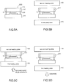
- the method of manufacturing a bonded body according to the embodiment 2 is characterized in that the method further includes, between an assembled body forming step and an assembled body arranging step, a pressure applying unit forming step for forming a pressure applying unit 200 in a state where the assembled body is sandwiched between two transfer members (a first transfer member 210, a second transfer member 220) which transfer pressure and heat (see Fig. 5A ), and in the assembled body arranging step (a pressure applying unit arranging step), the pressure applying unit 200 is arranged in a space defined between two heating plates (the first heating plate 120, the second heating plate 122) at a position where the pressure applying unit 200 is in contact with neither one of two heating plates (the first heating plate 120, the second heating plate 122) (see Fig. 5B ).
- a bonding step (see Fig. 5C ) is performed where at least one (the first heating plate 120) of two heating plates (the first heating plate 120, the second heating plate 122) is moved toward the other (the second heating plate 122) of two heating plates so that the substrate 12 and the electronic part 14 are bonded to each other by heating the assembled body 10 while indirectly applying pressure to the assembled body 10 by means of the pressure applying unit 200 (see Fig. 5C).
- 5D shows a state where two heating plates (the first heating plate 120, the second heating plate 122) are separated from each other by lowering the first heating plate 120 after the bonding step is finished so that it is possible to take out the pressure applying unit 200 and a bonded body 11 to the outside.
- the pressure applying unit 200 is arranged in a space defined between two heating plates (the first heating plate 120, the second heating plate 122) at a position where the pressure applying unit 200 is in contact with neither one of two heating plates (the first heating plate 120, the second heating plate 122) (see Fig. 5B ), and the bonding step is performed under a condition that a temperature T 1 of the assembled body at the time of starting applying of pressure to the assembled body 10 through the pressure applying unit 200 (that is, at the time of starting the applying of pressure) by two heating plates (the first heating plate 120, the second heating plate 122) falls within a range of from 0°C to 150°C.
- the assembled body arranging step as a method of arranging the pressure applying unit 200 in a space defined between two heating plates (the first heating plate 120, the second heating plate 122) at a position where the pressure applying unit 200 is in contact with neither one of two heating plates (the first heating plate 120, the second heating plate 122), a method which uses an arm substantially in the same manner as the embodiment 1 can be used. However, a method described later can be also used (see Fig. 6 to Fig. 10 described later).
- the pressure applying unit 200 is arranged in a space defined between two heating plates (the first heating plate 120, the second heating plate 122) at a position where the pressure applying unit 200 is in contact with neither one of two heating plates (the first heating plate 120, the second heating plate 122) (see Fig. 5B ) and hence, the bonding step is performed under a condition that a temperature T 1 of the assembled body at the time of starting applying of the pressure to the assembled body 10 (that is, at the time of starting the applying of pressure) by way of the pressure applying unit 200 by two heating plates (the first heating plate 120, the second heating plate 122) falls within a range of from 0°C to 150°C.
- a sintering reaction minimally occurs in a metal particle paste before pressure is applied to the assembled body.
- a substrate and an electronic part can be bonded to each other with a bonding strength higher than that of the prior art.
- a temperature T 1 of the assembled body 10 at the time of starting the applying of pressure can also be confirmed by the measurement of a temperature using a thermography or can be confirmed by the measurement of a temperature using a thermocouple.
- the assembled body 10 is formed substantially in the same manner as the embodiment 1.
- the pressure applying unit 200 includes a first transfer member 210, a second transfer member 220, guide members 230, and distance adjusting mechanisms 240.
- the pressure applying unit 200 sandwiches the assembled body 10 and transfers pressure and heat.
- the first transfer member 210 and the second transfer member 220 are connected to each other by way of the guide members 230.
- the first transfer member 210 is a plate-like member on which the assembled body 10 is mounted.
- the first transfer member 210 includes: a base portion 212 which projects outward from a center portion of a surface of the first transfer member 210 on a side opposite to a surface of the first transfer member 210 which faces the second transfer member 220 in an opposed manner; and shoulder portions 214 which are formed on the periphery of the base portion 212.
- the first transfer member 210 has an approximately quadrangular shape as viewed in a plan view, and the guide member 230 is formed in an erected manner on respective corner portions of the first transfer member 210.
- the second transfer member 220 is a flat-plate-like member which is brought into contact with the electronic part 14 when pressure is applied to the pressure applying unit.
- the second transfer member 220 has an approximately quadrangular shape as viewed in a plan view, and guide member receiving holes 222 are formed in the second transfer member 220 at positions corresponding to the guide members 230 (respective corner portions of the second transfer member 220).
- the guide members 230 are rod-like members for connecting the first transfer member 210 and the second transfer member 220 to each other.
- the guide members 230 guide the second transfer member 220 while keeping parallelism of the second transfer member 220 with the first transfer member 210.
- One end portions of the guide members 230 are connected to the first transfer member 210 at respective corner portions of the first transfer member 210, and the other end portions of the guide members 230 are inserted into the guide member receiving holes 222 respectively.
- the other end portions of the guide members 230 are configured such that the other end portions of the guide members 230 do not project from the guide member receiving holes 222 even when pressure is applied to the pressure applying unit 200.
- the distance adjusting mechanism 240 is a resilient member such as a coil spring for adjusting a distance between the first transfer member 210 and the second transfer member 220.
- the distance adjusting mechanisms 240 make the second transfer member 220 and the electronic part 14 separated from each other when pressure is not applied to the pressure applying unit 200, and brings the second transfer member 220 and the electronic part 14 into contact with each other when pressure is applied to the pressure applying unit 200.
- first transfer member 210 the first transfer member 210, the second transfer member 220
- metal tool steel, stainless steel, carbon steel, a hard metal alloy or the like
- ceramic silicon nitride, aluminum nitride, boron nitride, zirconia, silicon carbide, alumina or the like
- metal tool steel, stainless steel, carbon steel, a hard metal alloy or the like
- ceramic silicon nitride, aluminum nitride, boron nitride, zirconia, silicon carbide, alumina or the like
- the pressure applying unit includes both the pressure applying unit where the assembled body is sandwiched between two transfer members without forming a gap between the transfer member and the assembled body and the pressure applying unit where the assembled body is sandwiched between two transfer members while forming a gap between the transfer member and the assembled body.
- the pressure applying unit arranging step is performed using a tray 131 (see Fig. 6B ). Firstly, the base portion 212 of the first transfer member 210 is inserted into an opening portion 134 formed in the tray 131, and the pressure applying unit 200 is accommodated in the tray 131 in a state where the shoulder portions 214 of the first transfer member 210 are supported by support portions 135. Next, the tray 131 which accommodates the pressure applying unit 200 therein is mounted on tray receiving portions 137.
- the pressure applying unit 200 (and the assembled body 10) can be arranged in a space defined between the first heating plate 120 and the second heating plate 122 at a position where the pressure applying unit 200 is in contact with neither the first heating plate 120 nor the second heating plate 122 (see Fig. 7A ).
- the height position of the pressure applying unit 200 is an intermediate height position between the first heating plate 120 and the second heating plate 122.
- the first heating plate 120 is moved upward along an axis (along a vertical axis) extending toward the second heating plate 122 from the first heating plate 120 using a pressure applying mechanism portion not shown in the drawing.
- the first heating plate 120 and the second heating plate 122 are heated in advance. Both a heating temperature of the first heating plate 120 and a heating temperature of the second heating plate 122 are 300°C, for example.
- the first heating plate 120 When the first heating plate 120 is moved to a position where the first heating plate 120 is in contact with the first transfer member 210, the first heating plate 120 is brought into a state where the first heating plate 120 pushes the base portion 212 of the pressure applying unit 200. Accordingly, a state is brought about where the support portions 135 of the tray 131 are separated from the shoulder portions 214 of the pressure applying unit 200 (see a region surrounded by a broken line A in Fig. 7B ).
- the pressure applying unit 200 is also moved upward. Accordingly, a state is brought about where the tray 131 is in contact with the first heating plate 120 (see a region surrounded by a broken line A in Fig. 7C ).
- the pressure applying unit 200 and the tray 131 are also moved upward, and a state is brought about where the tray 131 is separated from the tray receiving portions 137 (see Fig. 8A ).
- the pressure applying unit 200 and the tray 131 are also moved upward, and a state is brought about where an upper surface of the second transfer member 220 of the assembled body 10 is in contact with the second heating plate 122 (see Fig. 8B ).
- heat is started to be transferred to the second transfer member 220 from the second heating plate 122 due to heat transfer.
- heat is not yet transferred to the assembled body 10.
- the first heating plate 120 When the first heating plate 120 is further moved upward, the first transfer member 210 and the assembled body 10 are also moved upward, and the upper surface of the electronic part 14 and the second transfer member 220 are brought into contact with each other (see Fig. 8C ).
- the pressure applying unit 200 is applied with pressure by the first heating plate 120 and the second heating plate 122, and pressure is applied to the assembled body 10 (the metal particle paste 16 of the assembled body 10) by the first heating plate 120 and the second heating plate 122 through the first transfer member 210 and the second transfer member 220. Further, heat is transferred to the metal particle paste 16 of the assembled body 10 by the first heating plate 120 and the second heating plate 122 through the first transfer member 210 and the second transfer member 220.
- the assembled body 10 can be heated while applying pressure to the assembled body 10 through the first transfer member 210 and the second transfer member 220 and hence, the metal particle paste 16 can be heated while applying pressure to the metal particle paste 16. As a result, the metal particle paste 16 is baked, and the substrate 12 and the electronic part 14 are bonded to each other thus manufacturing the bonded body 11.
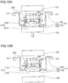
- the pressure applying unit 200 and the tray 131 are moved downward (see Fig. 9A to Fig. 9C and Fig. 10A ), and the tray 131 which accommodates the pressure applying unit 200 therein and the first heating plate 120 are made to return to respective initial positions (see Fig. 10B ). With such an operation, the pressure applying unit 200 is separated from both the first heating plate 120 and the second heating plate 122 and hence, it is possible to cool the pressure applying unit 200.
- the manufactured bonded body 11 can be taken out to the outside.
- a method of manufacturing a bonded body according to an embodiment 3 basically includes substantially the same steps as the method of manufacturing a bonded body according to the embodiment 1. However, the method of manufacturing a bonded body according to the embodiment 3 differs from the method of manufacturing a bonded body according to the embodiment 1 with respect to a temperature of a first heating plate and the content of an assembled body arranging step. That is, in the method of manufacturing a bonded body according to the embodiment 3, out of two heating plates, a first heating plate 120 is set to a temperature which falls within a range of from 50°C to 150°C (for example, 100°C), and a second heating plate 122 is set to a temperature which falls within a range of from 250°C to 350°C (for example, 300°C). Further, in the assembled body arranging step, the assembled body 10 is arranged at a position where the assembled body 10 is in contact with the first heating plate 120 (see Fig. 11 ).
- the method of manufacturing a bonded body according to the embodiment 3 differs from the method of manufacturing a bonded body according to the embodiment 1 with respect to a temperature of the first heating plate and the content of the assembled body arranging step.
- the first heating plate 120 is set to a temperature which falls within a range of from 50°C to 150°C (for example, 100°C)
- the second heating plate 122 is set to a temperature which falls within a range of from 250°C to 350°C (for example, 300°C) .
- the bonding step can be performed under a condition that a temperature T 1 of the assembled body at the time of starting applying of pressure to the assembled body 10 (that is, at the time of starting the applying of pressure) by two heating plates (the first heating plate 120, the second heating plate 122) falls within a range of from 0°C to 150°C (see a curve of the embodiment 3 in Fig. 12 ).
- a sintering reaction minimally occurs in a metal particle paste before pressure is applied to the assembled body.
- a substrate and an electronic part can be bonded to each other with a bonding strength higher than that of the prior art.
- a method of manufacturing a bonded body according to an embodiment 4 basically includes substantially the same steps as the method of manufacturing a bonded body according to the embodiment 2. However, the method of manufacturing a bonded body according to the embodiment 4 differs from the method of manufacturing a bonded body according to the embodiment 2 with respect to the content of a pressure applying unit arranging step. That is, in the method of manufacturing a bonded body according to the embodiment 4, in the pressure applying unit arranging step, a pressure applying unit 200 is directly mounted on a first heating plate 120 (see Fig. 13 ).
- the method of manufacturing a bonded body according to the embodiment 4 differs from the method of manufacturing a bonded body according to the embodiment 2 with respect to the content of the pressure applying unit arranging step.
- a substrate and an electronic part are not bonded to each other by heating the assembled body while directly applying pressure to the assembled body using two heating plates but are bonded to each other by heating while indirectly applying pressure to the assembled body using a pressure applying unit.
- a bonding step can be performed under a condition that a temperature T 1 of the assembled body at the time of starting applying of pressure to the assembled body 10 (that is, at the time of starting the applying of pressure) by two heating plates (the first heating plate 120, the second heating plate 122) falls within a range of from 0°C to 150°C.
- a sintering reaction minimally occurs in a metal particle paste before pressure is applied to the assembled body.
- the substrate and the electronic part can be bonded to each other with a bonding strength higher than that of the prior art.
Landscapes
- Die Bonding (AREA)
- Ceramic Products (AREA)
- Pressure Welding/Diffusion-Bonding (AREA)
Abstract


Description
- The present invention relates to a method of manufacturing a bonded body.
- There has been known a semiconductor device having a structure where a substrate on which a conductor pattern is formed and a semiconductor element are bonded to each other using a metal particle paste (see
patent literature 1, for example). The metal particle paste is a conductive paste of a low-temperature baking type which contains nano-sized or submicron-sized metal particles in a solvent, and makes use of a low-temperature sintering phenomenon and high surface activity of the metal particles. - As shown in
Fig. 18 , the above-mentioned semiconductor device can be manufactured by a following bonding step. An assembledbody 10 where asemiconductor element 14 is mounted on asubstrate 12 on which a conductor pattern is formed with ametal particle paste 16 interposed therebetween (seeFig. 18A ) is placed on an upper surface of afirst heating plate 920 on a lower side out of two heating plates (first heating plate 920 and second heating plate 922) (seeFig. 18B ). Thesecond heating plate 922 on an upper side is descended toward thefirst heating plate 920 thus heating the above-mentioned assembledbody 10 while applying pressure to the assembledbody 10 whereby thesubstrate 12 on which the conductor pattern is formed and thesemiconductor element 14 are bonded to each other (seeFig. 18C and Fig. 18D ). - Patent Literature 1:
JP-A-2012-9703 - However, in the above-mentioned method, heat is transferred to the
metal particle paste 16 from thefirst heating plate 920 due to the heat transfer before pressure is applied to the assembledbody 10 and hence, a sintering reaction (solidifying reaction) occurs in a portion of themetal particle paste 16. As a result, there arises a drawback that thesubstrate 12 on which a conductor pattern is formed and thesemiconductor element 16 cannot be bonded to each other with a high bonding strength. - Such a problem is not a problem which occurs only in manufacturing a semiconductor device having the structure where a substrate on which a conductor pattern is formed and a semiconductor element are bonded to each other using a metal particle paste, and is also a problem which is likely to occur in bonded bodies in general having the structure where "a substrate on which a conductor pattern is formed or another substrate" and "a semiconductor element or another electronic part" are bonded to each other using a metal particle paste.
- The present invention has been made to overcome the above-mentioned drawbacks, and it is an object of the present invention to provide a method of manufacturing a bonded body capable of bonding a substrate and an electronic part with a bonding strength higher than a bonding strength used in the prior art.
-
- [1] A method of manufacturing a bonded body of the present invention is a method of manufacturing a bonded body having a structure where a substrate and an electronic part are bonded to each other with a metal particle paste interposed therebetween, the method including: an assembled body forming step of forming an assembled body where the electronic part is mounted on the substrate with the metal particle paste interposed therebetween; an assembled body arranging step of arranging the assembled body between two heating plates arranged in an opposedly facing manner; and a bonding step of bonding the substrate and the electronic part to each other by heating while applying pressure to the assembled body by moving at least one of two heating plates to the other of two heating plates, wherein the bonding step is performed under a condition that a temperature of the assembled body at the time of starting applying of the pressure to the assembled body by two heating plates falls within a range of from 0°C to 150°C.
- [2] In the method of manufacturing a bonded body of the present invention, it is preferable that the bonding step be performed under a condition that the temperature of the assembled body at the time of starting applying of the pressure to the assembled body by two heating plates falls within a range of from 50°C to 135°C.
- [3] In the method of manufacturing a bonded body of the present invention, it is preferable that, in the assembled body arranging step, the assembled body be arranged in a space defined between two heating plates at a position where the assembled body is in contact with neither one of two heating plates.
- [4] In the method of manufacturing a bonded body of the present invention, it is preferable that the method of manufacturing a bonded body of the present invention further comprise, between the assembled body forming step and the assembled body arranging step, a pressure applying unit forming step for forming a pressure applying unit where the assembled body is sandwiched between two transfer members which transfer pressure and heat, and in the assembled body arranging step, the pressure applying unit be arranged in a space defined between two heating plates at a position where the pressure applying unit is in contact with neither one of two heating plates.
- [5] In the method of manufacturing a bonded body of the present invention, it is preferable that a first heating plate out of two heating plates be set to a temperature which falls within a range of from 50°C to 150°C, and a second heating plate out of two heating plates be set to a temperature which falls within a range of from 250°C to 350°C, and in the assembled body arranging step, the assembled body be arranged at a position where the assembled body is in contact with the first heating plate.
- [6] In the method of manufacturing a bonded body of the present invention, it is preferable that the method of manufacturing a bonded body of the present invention further comprise, between the assembled body forming step and the assembled body arranging step, a pressure applying unit forming step for forming a pressure applying unit where the assembled body is sandwiched between two transfer members which transfer pressure and heat, and in the assembled body arranging step, the pressure applying unit be arranged at a position where the pressure applying unit is in contact with either one of two heating plates.
- [7] In the method of manufacturing a bonded body of the present invention, it is preferable that, in the assembled body arranging step, in a state where two heat shielding plates are arranged at a position in a space defined between two heating plates where two heat shielding plates are brought into contact with neither one of two heating plates, the assembled body be arranged in a space defined between two heat shielding plates at a position where the assembled body is in contact with neither one of two heat shielding plates, and in the bonding step, at least one of two heating plates be moved toward the other of two heating plates after two heat shielding plates are retracted from the space defined between two heating plates.
- According to the method of manufacturing a bonded body of the present invention, the bonding step is performed under a condition that a temperature of the assembled body at the time of starting applying of pressure to the assembled body (that is, at the time of starting the applying of pressure of the assembled body) by two heating plates falls within a range of from 0°C to 150°C. Accordingly, in the bonding step, a sintering reaction (solidifying reaction) minimally occurs in a metal particle paste before pressure is applied to the assembled body. As a result, a substrate and an electronic part can be bonded to each other with a bonding strength higher than that of the prior art.
- In the method of manufacturing a bonded body of the present invention, the reason that the bonding step is performed under a condition that a temperature of the assembled body at the time of starting the applying of pressure is 150°C or below is as follows. That is, when the bonding step is performed under a condition that a temperature of the assembled body at the time of starting the applying of pressure is higher than 150°C, a sintering reaction is liable to occur in a metal particle paste before pressure is applied to the assembled body. As a result, there may be a case where bonding between a substrate and an electronic part with a bonding strength higher than that of the prior art becomes difficult. On the other hand, the reason that the bonding step is performed under a condition that a temperature of the assembled body at the time of starting the applying of pressure becomes 0°C or above is as follows. That is, when the bonding step is performed under a condition that a temperature of the assembled body at the time of starting the applying of pressure is lower than 0°C, it takes a long time until the assembled body is heated to a temperature which enables bonding. As a result, it takes a long time for bonding a substrate and an electronic part to each other thus giving rise to a case where productivity at the time of performing a bonding step is lowered.
-
-
Fig. 1A to Fig. 1D are views for explaining a method of manufacturing a bonded body according to anembodiment 1, whereinFig. 1A to Fig. 1D are views showing respective steps. -
Fig. 2 is a view schematically showing a change in temperature of an assembled body according to theembodiment 1 and, inFig. 2 , symbol TRT indicates a room temperature. -
Fig. 3A to Fig. 3D are views for explaining one example of the method of manufacturing the bonded body according to theembodiment 1, whereinFig. 3A to Fig. 3D are views showing respective steps. -
Fig. 4A to Fig. 4D are views for explaining one example of the method of manufacturing the bonded body according to theembodiment 1, whereinFig. 4A to Fig. 4D are views showing respective steps. -
Fig. 5A to Fig. 5D are views for explaining a method of manufacturing a bonded body according to an embodiment 2, whereinFig. 5A to Fig. 5D are views showing respective steps. -
Fig. 6A and Fig. 6B are views for explaining apressure applying unit 200 and atray 131 which can be used in the embodiment 2, whereinFig. 6A is a cross-sectional view of thepressure applying unit 200, andFig. 6B is a perspective view of thetray 131. -
Fig. 7A to Fig. 7C are views for explaining one example of the method of manufacturing a bonded body according to the embodiment 2, whereinFig. 7A to Fig. 7C are views showing the respective steps. -
Fig. 8A to Fig. 8C are views for explaining one example of the method of manufacturing a bonded body according to the embodiment 2, whereinFig. 8A to Fig. 8C are views showing the respective steps. -
Fig. 9A to Fig. 9C are views for explaining one example of a method of manufacturing a bonded body according to the embodiment 2, whereinFig. 9A to Fig. 9C are views showing respective steps. -
Fig. 10A and Fig. 10B are views for explaining one example of a method of manufacturing a bonded body according to the embodiment 2, whereinFig. 10A and Fig. 10B are views showing respective steps. -
Fig. 11A to Fig. 11D are views for explaining a method of manufacturing a bonded body according to anembodiment 3, whereinFig. 11A to Fig. 11D are views showing respective steps. -
Fig. 12 is a view schematically showing a change in temperature of an assembled body according to theembodiment 3. InFig. 12 , symbol TRT indicates a room temperature. -
Fig. 13A to Fig. 13D are views for explaining a method of manufacturing a bonded body according to an embodiment 4, whereinFig. 13A to Fig. 13D are views showing respective steps . -
Fig. 14A to Fig. 14D are views for explaining a method of manufacturing a bonded body according to amodification 1, whereinFig. 14A to Fig. 14D are views showing respective steps. -
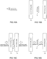
Fig. 15A to Fig. 15D are views for explaining a method of manufacturing a bonded body according to a modification 2, whereinFig. 15A to Fig. 15D are views showing respective steps. -
Fig. 16A to Fig. 16D are views for explaining a method of manufacturing a bonded body according to amodification 3, whereinFig. 16A to Fig. 16D are views showing respective steps. -
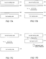
Fig. 17A to Fig. 17D are views for explaining a method of manufacturing a bonded body according to a modification 4, whereinFig. 17A to Fig. 17D are views showing respective steps . -
Fig. 18A to Fig. 18D are views for explaining a conventional method of manufacturing a bonded body, whereinFig. 18A to Fig. 18D are views showing respective steps. - Hereinafter, a method of manufacturing a bonded body of the present invention is explained by reference to embodiments shown in the drawings.
- As shown in
Fig. 1 , a method of manufacturing a bonded body according to anembodiment 1 is a method of manufacturing a bonded body for manufacturing a bonded body 11 (semiconductor device) having the structure where a substrate 12 (a substrate on which a conductor pattern is formed) and an electronic part 14 (semiconductor element) are bonded to each other with ametal particle paste 16 interposed therebetween (a method of manufacturing a semiconductor device). - The
substrate 12, theelectronic part 14, and themetal particle paste 16 are explained in detail. - In this specification, "substrate" means a part on which an electronic part is mounted.
- The
substrate 12 mounts theelectronic part 14 thereon. Thesubstrate 12 of theembodiment 1 is, for example, a printed circuit board where a conductor pattern is formed on a body made of a non-conductive material. As a material for forming thesubstrate 12, a material which has resistance to a sintering temperature of a metal particle paste 16 (for example, 300°C although the sintering temperature depends on a kind of material) can be used. For example, a resin or a ceramic having heat resistance is used for forming the body, and metal is used for forming the conductor pattern. - The substrate to which the present invention is applicable may be a DCB (Direct Copper Bond) substrate or a lead frame. Further, it is sufficient that the substrate to which the present invention is applicable is a substrate on which an electronic part can be mounted. For example, the substrate may be a silicon chip. That is, the present invention is also applicable to the connection between a silicon chip and a conductive connector.
- In this specification, "electronic part" means a part which is used in an electric product and is particularly required to be electrically connected to the substrate.
- The
electronic part 14 is a semiconductor element, for example. - As the
electronic part 14, besides the above-mentioned semiconductor element (for example, a semiconductor chip on which an integrated circuit is mounted), an electric motor, a resistor, a capacitor, a piezoelectric element, a connector, a switch, an antenna, and a conductive connector can be exemplified. The method of manufacturing a bonded body of the present invention is particularly preferably applicable to a case where a bonded body formed by bonding at least one semiconductor element and a substrate to each other, that is, a semiconductor device is manufactured. Although the number ofelectronic parts 14 used in theembodiment 1 is one, the present invention is also applicable to the case where two or more electronic parts are used. When two or more electronic parts are used, the electronic parts may be formed of one kind of electronic part, or may be formed of plural kinds of electronic parts. - The
metal particle paste 16 is a low-temperature baking-type conductive paste which makes use of low-temperature sintering phenomenon brought about by a quantum size effect of metal particles and high surface activity of the metal particles . Themetal particle paste 16 contains metal particles, an organic dispersion material, an organic dispersion material capturing material, and a volatile organic solvent, for example. As the metal particles, metal particles formed of metal nanoparticles (for example, metal particles having an average diameter of approximately 100nm or less), metal particles formed of metal submicron particles (for example, metal particles having an average diameter which falls within a range of from approximately 0. 1µm to approximately 1µm), or metal particles formed of both the metal nanoparticles and the metal submicron particles can be used. As a material for forming metal particles, silver, gold or copper can be used, for example. The organic dispersion material covers surfaces of metal particles at a room temperature, and performs a function of holding metal particles in an independently dispersed state. The organic dispersion material capturing material reacts with the organic dispersion material which covers metal particles at a high temperature and performs a function of removing the organic dispersion material from a surface of the metal particle. The volatile organic solvent has a function of capturing a chemical reaction product formed between the organic dispersion material and the organic dispersion material capturing material and also performs a function of releasing the chemical reaction product to the outside of a system in the form of a gas. - The method of manufacturing a bonded body according to the
embodiment 1 includes: an assembled body forming step of forming an assembledbody 10 where theelectronic part 14 is mounted on thesubstrate 12 with themetal particle paste 16 interposed therebetween (seeFig. 1A ); an assembled body arranging step of arranging the assembledbody 10 between two heating plates (afirst heating plate 120, a second heating plate 122) arranged in an opposedly facing manner (seeFig. 1B ); and a bonding step of bonding thesubstrate 12 and theelectronic part 14 to each other by heating while applying pressure to the assembledbody 10 by moving at least one (the first heating plate 120) of two heating plates (thefirst heating plate 120, the second heating plate 122) to the other (the second heating plate 122) of two heating plates (seeFig. 1C). Fig. 1D shows a state where two heating plates (thefirst heating plate 120, the second heating plate 122) are separated from each other by lowering thefirst heating plate 120 after the bonding step is finished, and a bondedbody 11 can be taken out to the outside. - In the method of manufacturing a bonded body according to the
embodiment 1, in the assembled body arranging step, the assembledbody 10 is arranged in a space defined between two heating plates (thefirst heating plate 120, the second heating plate 122) at a position where the assembledbody 10 is in contact with neither one of two heating plates (thefirst heating plate 120, the second heating plate 122) (seeFig. 1B ) and hence, the bonding step is performed under a condition that a temperature T1 (a first temperature T1) of the assembled body at the time of starting applying of the pressure to the assembled body 10 (that is, at the time of starting the applying of pressure) by two heating plates (thefirst heating plate 120, the second heating plate 122) falls within a range of from 0°C to 150°C (seeFig. 2 ). A specific method of arranging the assembledbody 10 in a space defined between two heating plates (thefirst heating plate 120, and the second heating plate 122) at a position where the assembledbody 10 is in contact with neither one of two heating plates (thefirst heating plate 120, the second heating plate 122) in the assembled body arranging step is described later (seeFig. 3 andFig. 4 described later). - According to the method of manufacturing a bonded body of the
embodiment 1, in the assembled body arranging step, the assembledbody 10 is arranged in a space defined between two heating plates (thefirst heating plate 120, the second heating plate 122) at a position where the assembledbody 10 is in contact with neither one of two heating plates (thefirst heating plate 120, the second heating plate 122) (seeFig. 1B ). Accordingly, the bonding step is performed under a condition that a temperature T1 of the assembled body at the time of starting applying of pressure to the assembled body 10 (that is, at the time of starting the applying of pressure) by two heating plates (thefirst heating plate 120, the second heating plate 122) falls within a range of from 0°C to 150°C (see a curve of theembodiment 1 shown inFig. 2 ). Accordingly, in the bonding step, a sintering reaction minimally occurs in a metal particle paste before pressure is applied to the assembled body. As a result, a substrate and an electronic part can be bonded to each other with a bonding strength higher than that of the prior art. - In the method of manufacturing a bonded body according to the
embodiment 1, the reason that the bonding step is performed under a condition that a temperature T1 of the assembled body at the time of starting the applying of pressure is 150°C or below is as follows. That is, when the bonding step is performed under a condition that a temperature T1 of the assembled body at the time of starting the applying of pressure is higher than 150°C (see a curve of the prior art shown inFig. 2 ), a sintering reaction is liable to occur in a metal particle paste before pressure is applied to the assembled body. As a result, there may be a case where bonding between a substrate and an electronic part with a bonding strength higher than that of the prior art becomes difficult. From this point of view, it is preferable to perform the bonding step under a condition that a temperature T1 of the assembled body at the time of starting the applying of pressure is 135°C or below, and it is more preferable to perform the bonding step under a condition that a temperature T1 of the assembled body at the time of starting the applying of pressure is 120°C or below. - On the other hand, the reason that the bonding step is performed under a condition that a temperature T1 of the assembled
body 10 at the time of starting the applying of pressure is 0°C or above is as follows. That is, when the bonding step is performed under a condition that a temperature T1 of the assembledbody 10 at the time of starting the applying of pressure is lower than 0°C, it takes a long time until the assembled body is heated to a temperature which enables bonding. As a result, it takes a long time for bonding a substrate and an electronic part to each other thus giving rise to a case where productivity at the time of performing the bonding step is lowered. From this point of view, it is preferable to perform the bonding step under a condition that a temperature T1 of the assembledbody 10 at the time of starting the applying of pressure is 50°C or above, and it is more preferable to perform the bonding step under a condition that a temperature T1 of the assembledbody 10 at the time of starting the applying of pressure is 75°C or above. - A temperature T1 of the assembled
body 10 at the time of starting the applying of pressure can be confirmed by the measurement of a temperature using a thermography. As a temperature T1 of the assembledbody 10, it is preferable to use a temperature of themetal particle paste 16 sandwiched between thesubstrate 12 and theelectronic part 14. However, for the sake of convenience, a temperature of thesubstrate 12, a temperature of theelectronic part 14, or an average temperature of the assembledbody 10 can be also used. Further, a temperature T1 of the assembledbody 10 can be confirmed also by the measurement of a temperature using a thermocouple. As a temperature T1 of the assembledbody 10, a temperature obtained by bringing a distal end portion of a thermocouple to any portion of thesubstrate 12 or theelectronic part 14 and by converting an output voltage of the thermocouple into a temperature can be used. In this case, a temperature T1 of the assembledbody 10 is confirmed and, thereafter, the thermocouple is retracted and, then, the bonding step is performed so that the bonding between thesubstrate 12 and the electronic part can be properly performed. Further, a temperature elevation curve of the assembled body is measured in a preliminary examination performed prior to the bonding step, and an operation of arranging the assembled body and an operation of elevating the first, heating plate properly over steps ranging from the assembled body arranging step to the bonding step by taking into account the temperature elevation curve, thesubstrate 12 and the electronic part can be properly bonded to each other. - One example of the method of manufacturing a bonded body according to the
embodiment 1 is explained in detail by reference toFig. 3 andFig. 4 . - Firstly, the assembled
body 10 where theelectronic part 14 is mounted on thesubstrate 12 with themetal particle paste 16 interposed therebetween is formed. - Next, the assembled
body 10 is held by an arm 124 (seeFig. 3A ) and, thereafter, using thearm 124, the assembledbody 10 is arranged between two heating plates (thefirst heating plate 120, the second heating plate 122) which are arranged to face each other in an opposed manner (seeFig. 3B ). - Next, the
first heating plate 120 is elevated so as to bring thefirst heating plate 120 into contact with a lower surface of the assembled body 10 (seeFig. 3C ) and thereafter, thearm 124 is removed from the assembled body 10 (seeFig. 3D ) . Then, thefirst heating plate 120 is further elevated with the assembledbody 10 mounted on thefirst heating plate 120 thus bringing an upper surface of the assembledbody 10 into contact with thesecond heating plate 122. Thereafter, thefirst heating plate 120 is further elevated (moved) toward thesecond heating plate 122 and hence, the assembledbody 10 is heated while being applied with pressure at a predetermined pressure whereby thesubstrate 12 and theelectronic part 14 are bonded to each other (seeFig. 4A ). - Temperatures of both two heating plates (the
first heating plate 120, the second heating plate 122) are set to 300°C, for example. Two heating plates (thefirst heating plate 120, the second heating plate 122) respectively have a flat plate shape, and surfaces of each heating plate opposite to each other are set parallel to each other. Although various kinds of materials can be used as a material for forming two heating plates (thefirst heating plate 120, the second heating plate 122), for example, stainless steel, die making steel or the like can be preferably used. - When the bonding step is finished, the
first heating plate 120 is lowered (seeFig. 4B ) so as to bring about a state where two heating plates (thefirst heating plate 120, the second heating plate 122) are separated from each other at a predetermined distance. Then, the bondedbody 11 is held by the arm 124 (seeFig. 4C ) and, thereafter, thefirst heating plate 120 is further lowered (seeFig. 4D ) thus returning thefirst heating plate 120 to the initial position. At this stage of the operation, the bondedbody 11 is held by thearm 124 and hence, the bondedbody 11 can be taken out by thearm 124 to the outside from a space defined between thefirst heating plate 120 and thesecond heating plate 122. - A method of manufacturing a bonded body according to an embodiment 2 includes substantially the same steps as the method of manufacturing a bonded body according to the
embodiment 1. However, the method of manufacturing a bonded body according to the embodiment 2 differs from the method of manufacturing a bonded body according to theembodiment 1 with respect to a point that a substrate and an electronic part are not bonded to each other by heating an assembled body while directly applying pressure to the assembled body using two heating plates but the substrate and the electronic part are bonded to each other by heating while indirectly applying pressure to the assembled body using a pressure applying unit. That is, as shown inFig. 5 , the method of manufacturing a bonded body according to the embodiment 2 is characterized in that the method further includes, between an assembled body forming step and an assembled body arranging step, a pressure applying unit forming step for forming apressure applying unit 200 in a state where the assembled body is sandwiched between two transfer members (afirst transfer member 210, a second transfer member 220) which transfer pressure and heat (seeFig. 5A ), and in the assembled body arranging step (a pressure applying unit arranging step), thepressure applying unit 200 is arranged in a space defined between two heating plates (thefirst heating plate 120, the second heating plate 122) at a position where thepressure applying unit 200 is in contact with neither one of two heating plates (thefirst heating plate 120, the second heating plate 122) (seeFig. 5B ). - In the method of manufacturing a bonded body according to the embodiment 2, after the assembled body arranging step is performed, a bonding step (see
Fig. 5C ) is performed where at least one (the first heating plate 120) of two heating plates (thefirst heating plate 120, the second heating plate 122) is moved toward the other (the second heating plate 122) of two heating plates so that thesubstrate 12 and theelectronic part 14 are bonded to each other by heating the assembledbody 10 while indirectly applying pressure to the assembledbody 10 by means of the pressure applying unit 200 (seeFig. 5C). Fig. 5D shows a state where two heating plates (thefirst heating plate 120, the second heating plate 122) are separated from each other by lowering thefirst heating plate 120 after the bonding step is finished so that it is possible to take out thepressure applying unit 200 and a bondedbody 11 to the outside. - Further, in the method of manufacturing a bonded body according to the embodiment 2, in the assembled body arranging step, the
pressure applying unit 200 is arranged in a space defined between two heating plates (thefirst heating plate 120, the second heating plate 122) at a position where thepressure applying unit 200 is in contact with neither one of two heating plates (thefirst heating plate 120, the second heating plate 122) (seeFig. 5B ), and the bonding step is performed under a condition that a temperature T1 of the assembled body at the time of starting applying of pressure to the assembledbody 10 through the pressure applying unit 200 (that is, at the time of starting the applying of pressure) by two heating plates (thefirst heating plate 120, the second heating plate 122) falls within a range of from 0°C to 150°C. In the assembled body arranging step, as a method of arranging thepressure applying unit 200 in a space defined between two heating plates (thefirst heating plate 120, the second heating plate 122) at a position where thepressure applying unit 200 is in contact with neither one of two heating plates (thefirst heating plate 120, the second heating plate 122), a method which uses an arm substantially in the same manner as theembodiment 1 can be used. However, a method described later can be also used (seeFig. 6 to Fig. 10 described later). - According to the method of manufacturing a bonded body of the embodiment 2, in the assembled body arranging step, the
pressure applying unit 200 is arranged in a space defined between two heating plates (thefirst heating plate 120, the second heating plate 122) at a position where thepressure applying unit 200 is in contact with neither one of two heating plates (thefirst heating plate 120, the second heating plate 122) (seeFig. 5B ) and hence, the bonding step is performed under a condition that a temperature T1 of the assembled body at the time of starting applying of the pressure to the assembled body 10 (that is, at the time of starting the applying of pressure) by way of thepressure applying unit 200 by two heating plates (thefirst heating plate 120, the second heating plate 122) falls within a range of from 0°C to 150°C. Accordingly, in the bonding step, a sintering reaction minimally occurs in a metal particle paste before pressure is applied to the assembled body. As a result, a substrate and an electronic part can be bonded to each other with a bonding strength higher than that of the prior art. - As has been explained in the
embodiment 1, a temperature T1 of the assembledbody 10 at the time of starting the applying of pressure can also be confirmed by the measurement of a temperature using a thermography or can be confirmed by the measurement of a temperature using a thermocouple. - One example of a method of manufacturing a bonded body according to the embodiment 2 is explained in detail by reference to
Fig. 6 to Fig. 10 . - The assembled
body 10 is formed substantially in the same manner as theembodiment 1. - As shown in
Fig. 6A , thepressure applying unit 200 includes afirst transfer member 210, asecond transfer member 220, guidemembers 230, anddistance adjusting mechanisms 240. Thepressure applying unit 200 sandwiches the assembledbody 10 and transfers pressure and heat. Thefirst transfer member 210 and thesecond transfer member 220 are connected to each other by way of theguide members 230. - The
first transfer member 210 is a plate-like member on which the assembledbody 10 is mounted. Thefirst transfer member 210 includes: abase portion 212 which projects outward from a center portion of a surface of thefirst transfer member 210 on a side opposite to a surface of thefirst transfer member 210 which faces thesecond transfer member 220 in an opposed manner; andshoulder portions 214 which are formed on the periphery of thebase portion 212. Thefirst transfer member 210 has an approximately quadrangular shape as viewed in a plan view, and theguide member 230 is formed in an erected manner on respective corner portions of thefirst transfer member 210. - The
second transfer member 220 is a flat-plate-like member which is brought into contact with theelectronic part 14 when pressure is applied to the pressure applying unit. Thesecond transfer member 220 has an approximately quadrangular shape as viewed in a plan view, and guidemember receiving holes 222 are formed in thesecond transfer member 220 at positions corresponding to the guide members 230 (respective corner portions of the second transfer member 220). - The
guide members 230 are rod-like members for connecting thefirst transfer member 210 and thesecond transfer member 220 to each other. Theguide members 230 guide thesecond transfer member 220 while keeping parallelism of thesecond transfer member 220 with thefirst transfer member 210. One end portions of theguide members 230 are connected to thefirst transfer member 210 at respective corner portions of thefirst transfer member 210, and the other end portions of theguide members 230 are inserted into the guidemember receiving holes 222 respectively. The other end portions of theguide members 230 are configured such that the other end portions of theguide members 230 do not project from the guidemember receiving holes 222 even when pressure is applied to thepressure applying unit 200. - The
distance adjusting mechanism 240 is a resilient member such as a coil spring for adjusting a distance between thefirst transfer member 210 and thesecond transfer member 220. Thedistance adjusting mechanisms 240 make thesecond transfer member 220 and theelectronic part 14 separated from each other when pressure is not applied to thepressure applying unit 200, and brings thesecond transfer member 220 and theelectronic part 14 into contact with each other when pressure is applied to thepressure applying unit 200. - Although various materials can be used as a material for forming two transfer members (the
first transfer member 210, the second transfer member 220), metal (tool steel, stainless steel, carbon steel, a hard metal alloy or the like), ceramic (silicon nitride, aluminum nitride, boron nitride, zirconia, silicon carbide, alumina or the like) or the like may preferably be used, for example. - As can be understood from
Fig. 5A andFig. 6A , the pressure applying unit includes both the pressure applying unit where the assembled body is sandwiched between two transfer members without forming a gap between the transfer member and the assembled body and the pressure applying unit where the assembled body is sandwiched between two transfer members while forming a gap between the transfer member and the assembled body. - In the embodiment 2, the pressure applying unit arranging step is performed using a tray 131 (see
Fig. 6B ). Firstly, thebase portion 212 of thefirst transfer member 210 is inserted into anopening portion 134 formed in thetray 131, and thepressure applying unit 200 is accommodated in thetray 131 in a state where theshoulder portions 214 of thefirst transfer member 210 are supported bysupport portions 135. Next, thetray 131 which accommodates thepressure applying unit 200 therein is mounted ontray receiving portions 137. Due to such an operation, the pressure applying unit 200 (and the assembled body 10) can be arranged in a space defined between thefirst heating plate 120 and thesecond heating plate 122 at a position where thepressure applying unit 200 is in contact with neither thefirst heating plate 120 nor the second heating plate 122 (seeFig. 7A ). At this stage of the operation, the height position of thepressure applying unit 200 is an intermediate height position between thefirst heating plate 120 and thesecond heating plate 122. - Next, the
first heating plate 120 is moved upward along an axis (along a vertical axis) extending toward thesecond heating plate 122 from thefirst heating plate 120 using a pressure applying mechanism portion not shown in the drawing. - The
first heating plate 120 and thesecond heating plate 122 are heated in advance. Both a heating temperature of thefirst heating plate 120 and a heating temperature of thesecond heating plate 122 are 300°C, for example. - When the
first heating plate 120 is moved to a position where thefirst heating plate 120 is in contact with thefirst transfer member 210, thefirst heating plate 120 is brought into a state where thefirst heating plate 120 pushes thebase portion 212 of thepressure applying unit 200. Accordingly, a state is brought about where thesupport portions 135 of thetray 131 are separated from theshoulder portions 214 of the pressure applying unit 200 (see a region surrounded by a broken line A inFig. 7B ). - When the
first heating plate 120 is further moved upward from such a state, thepressure applying unit 200 is also moved upward. Accordingly, a state is brought about where thetray 131 is in contact with the first heating plate 120 (see a region surrounded by a broken line A inFig. 7C ). - When the
first heating plate 120 is further moved upward from such a state, thepressure applying unit 200 and thetray 131 are also moved upward, and a state is brought about where thetray 131 is separated from the tray receiving portions 137 (seeFig. 8A ). - When the
first heating plate 120 is further moved upward from such a state, thepressure applying unit 200 and thetray 131 are also moved upward, and a state is brought about where an upper surface of thesecond transfer member 220 of the assembledbody 10 is in contact with the second heating plate 122 (seeFig. 8B ). At this stage of the operation, heat is started to be transferred to thesecond transfer member 220 from thesecond heating plate 122 due to heat transfer. However, heat is not yet transferred to the assembledbody 10. - When the
first heating plate 120 is further moved upward, thefirst transfer member 210 and the assembledbody 10 are also moved upward, and the upper surface of theelectronic part 14 and thesecond transfer member 220 are brought into contact with each other (seeFig. 8C ). - In such a state, by moving the
first heating plate 120 more upward as described above, thepressure applying unit 200 is applied with pressure by thefirst heating plate 120 and thesecond heating plate 122, and pressure is applied to the assembled body 10 (themetal particle paste 16 of the assembled body 10) by thefirst heating plate 120 and thesecond heating plate 122 through thefirst transfer member 210 and thesecond transfer member 220. Further, heat is transferred to themetal particle paste 16 of the assembledbody 10 by thefirst heating plate 120 and thesecond heating plate 122 through thefirst transfer member 210 and thesecond transfer member 220. - The assembled
body 10 can be heated while applying pressure to the assembledbody 10 through thefirst transfer member 210 and thesecond transfer member 220 and hence, themetal particle paste 16 can be heated while applying pressure to themetal particle paste 16. As a result, themetal particle paste 16 is baked, and thesubstrate 12 and theelectronic part 14 are bonded to each other thus manufacturing the bondedbody 11. - By moving the
first heating plate 120 downward after baking themetal particle paste 16, thepressure applying unit 200 and thetray 131 are moved downward (seeFig. 9A to Fig. 9C andFig. 10A ), and thetray 131 which accommodates thepressure applying unit 200 therein and thefirst heating plate 120 are made to return to respective initial positions (seeFig. 10B ). With such an operation, thepressure applying unit 200 is separated from both thefirst heating plate 120 and thesecond heating plate 122 and hence, it is possible to cool thepressure applying unit 200. - In this manner, the manufactured bonded
body 11 can be taken out to the outside. - A method of manufacturing a bonded body according to an
embodiment 3 basically includes substantially the same steps as the method of manufacturing a bonded body according to theembodiment 1. However, the method of manufacturing a bonded body according to theembodiment 3 differs from the method of manufacturing a bonded body according to theembodiment 1 with respect to a temperature of a first heating plate and the content of an assembled body arranging step. That is, in the method of manufacturing a bonded body according to theembodiment 3, out of two heating plates, afirst heating plate 120 is set to a temperature which falls within a range of from 50°C to 150°C (for example, 100°C), and asecond heating plate 122 is set to a temperature which falls within a range of from 250°C to 350°C (for example, 300°C). Further, in the assembled body arranging step, the assembledbody 10 is arranged at a position where the assembledbody 10 is in contact with the first heating plate 120 (seeFig. 11 ). - In this manner, the method of manufacturing a bonded body according to the
embodiment 3 differs from the method of manufacturing a bonded body according to theembodiment 1 with respect to a temperature of the first heating plate and the content of the assembled body arranging step. However, as described above, out of two heating plates, thefirst heating plate 120 is set to a temperature which falls within a range of from 50°C to 150°C (for example, 100°C), and thesecond heating plate 122 is set to a temperature which falls within a range of from 250°C to 350°C (for example, 300°C) . Accordingly, the bonding step can be performed under a condition that a temperature T1 of the assembled body at the time of starting applying of pressure to the assembled body 10 (that is, at the time of starting the applying of pressure) by two heating plates (thefirst heating plate 120, the second heating plate 122) falls within a range of from 0°C to 150°C (see a curve of theembodiment 3 inFig. 12 ). As a result, in the same manner as the method of manufacturing a bonded body according to theembodiment 1, in the bonding step, a sintering reaction minimally occurs in a metal particle paste before pressure is applied to the assembled body. As a result, a substrate and an electronic part can be bonded to each other with a bonding strength higher than that of the prior art. - A method of manufacturing a bonded body according to an embodiment 4 basically includes substantially the same steps as the method of manufacturing a bonded body according to the embodiment 2. However, the method of manufacturing a bonded body according to the embodiment 4 differs from the method of manufacturing a bonded body according to the embodiment 2 with respect to the content of a pressure applying unit arranging step. That is, in the method of manufacturing a bonded body according to the embodiment 4, in the pressure applying unit arranging step, a
pressure applying unit 200 is directly mounted on a first heating plate 120 (seeFig. 13 ). - As described above, the method of manufacturing a bonded body according to the embodiment 4 differs from the method of manufacturing a bonded body according to the embodiment 2 with respect to the content of the pressure applying unit arranging step. However, in the same manner as the case of the method of manufacturing a bonded body according to the embodiment 2, a substrate and an electronic part are not bonded to each other by heating the assembled body while directly applying pressure to the assembled body using two heating plates but are bonded to each other by heating while indirectly applying pressure to the assembled body using a pressure applying unit. Accordingly, even when both temperatures of two heating plates (a
first heating plate 120, a second heating plate 122) are 300°C, a bonding step can be performed under a condition that a temperature T1 of the assembled body at the time of starting applying of pressure to the assembled body 10 (that is, at the time of starting the applying of pressure) by two heating plates (thefirst heating plate 120, the second heating plate 122) falls within a range of from 0°C to 150°C. As a result, in the same manner as the case of the method of manufacturing a bonded body according to the embodiment 2, in the bonding step, a sintering reaction minimally occurs in a metal particle paste before pressure is applied to the assembled body. As a result, the substrate and the electronic part can be bonded to each other with a bonding strength higher than that of the prior art. - Although the present invention has been explained heretofore by reference to the above-mentioned embodiments, the present invention is not limited to the above-mentioned embodiments. Various modifications are conceivable without departing from the gist of the present invention. For example, following modifications are also conceivable.
-
- (1) The number, materials, shapes, positions, sizes and the like of the constitutional elements described in the above-mentioned embodiments are merely examples, and can be changed within a range where advantageous effects of the present invention are not impaired.
- (2) In the above-mentioned
embodiment 1, thesubstrate 12 and theelectronic part 14 are bonded to each other by heating while applying pressure to the assembledbody 10 by moving thefirst heating plate 120 upward. However, the present invention is not limited to such a configuration. As shown inFig. 14 , thesubstrate 12 and theelectronic part 14 may be bonded to each other by heating while applying pressure to the assembledbody 10 by moving thesecond heating plate 122 downward (modification 1). As shown inFig. 15 , thesubstrate 12 and theelectronic part 14 may be bonded to each other by heating while applying pressure to the assembledbody 10 by moving thefirst heating plate 120 upward and by moving thesecond heating plate 122 downward (modification 2). As shown inFig. 16 , thesubstrate 12 and theelectronic part 14 may be bonded to each other by heating while applying pressure to the assembledbody 10 by moving thefirst heating plate 120 and/or thesecond heating plate 122 in the transverse direction (modification 3). - (3) In the present invention, as shown in
Fig. 17 , in the assembled body arranging step, in a state where two heat shielding plates (a firstheat shielding plate 150, a second heat shielding plate 152) are arranged at a position in a space defined between two heating plates (afirst heating plate 120, a second heating plate 122) where two heat shielding plates (the firstheat shielding plate 150, the second heat shielding plate 152) are brought into contact with neither one of two heating plates (thefirst heating plate 120, the second heating plate 122), the assembledbody 10 may be arranged in a space defined between two heat shielding plates (the firstheat shielding plate 150, the second heat shielding plate 152) at a position where the assembledbody 10 is in contact with neither one of two heat shielding plates (the firstheat shielding plate 150, the second heat shielding plate 152). Further, in the bonding step, at least one of two heating plates (thefirst heating plate 120, the second heating plate 122) may be moved toward the other of two heating plates after two heat shielding plates (the firstheat shielding plate 150, the second heat shielding plate 152) are retracted from the space defined between two heating plates (thefirst heating plate 120, the second heating plate 122). -
- 10:
- assembled body
- 11:
- bonded body
- 12:
- substrate
- 14:
- electronic part
- 16:
- metal particle paste
- 120:
- first heating plate
- 122:
- second heating plate
- 131:
- tray
- 132:
- positioning portion
- 133:
- bottom surface
- 134:
- opening portion
- 135:
- support portion
- 136:
- folded portion (of tray)
- 137:
- tray receiving portion
- 150, 152:
- heat shielding plate
- 200:
- pressure applying unit
- 210:
- first transfer member
- 212:
- base portion
- 214:
- shoulder portion
- 220:
- second transfer member
- 222:
- guide member receiving hole
- 230:
- guide member
- 240:
- distance adjusting mechanism
Claims (7)
- A method of manufacturing a bonded body having a structure where a substrate and an electronic part are bonded to each other with a metal particle paste interposed therebetween, the method comprising:an assembled body forming step of forming an assembled body where the electronic part is mounted on the substrate with the metal particle paste interposed therebetween;an assembled body arranging step of arranging the assembled body between two heating plates arranged in an opposedly facing manner; anda bonding step of bonding the substrate and the electronic part to each other by heating while applying pressure to the assembled body by moving at least one of said two heating plates to the other of said two heating plates, whereinthe bonding step is performed under a condition that a temperature of the assembled body at the time of starting applying of the pressure to the assembled body by said two heating plates falls within a range of from 0°C to 150°C.
- The method of manufacturing a bonded body according to claim 1, wherein the bonding step is performed under a condition that the temperature of the assembled body at the time of starting applying of the pressure to the assembled body by said two heating plates falls within a range of from 50°C to 135°C.
- The method of manufacturing a bonded body according to claim 1 or 2, wherein in the assembled body arranging step, the assembled body is arranged in a space defined between said two heating plates at a position where the assembled body is in contact with neither one of said two heating plates.
- The method of manufacturing a bonded body according to claim 1 or 2, wherein the method of manufacturing a bonded body further comprises, between the assembled body forming step and the assembled body arranging step, a pressure applying unit forming step for forming a pressure applying unit where the assembled body is sandwiched between two transfer members which transfer pressure and heat, and
in the assembled body arranging step, the pressure applying unit is arranged in a space defined between said two heating plates at a position where the pressure applying unit is in contact with neither one of said two heating plates. - The method of manufacturing a bonded body according to claim 1 or 2, wherein a first heating plate out of said two heating plates is set to a temperature which falls within a range of from 50°C to 150°C, and a second heating plate out of said two heating plates is set to a temperature which falls within a range of from 250°C to 350°C, and
in the assembled body arranging step, the assembled body is arranged at a position where the assembled body is in contact with the first heating plate. - The method of manufacturing a bonded body according to claim 1 or 2, wherein the method of manufacturing a bonded body further comprises, between the assembled body forming step and the assembled body arranging step, a pressure applying unit forming step for forming a pressure applying unit where the assembled body is sandwiched between two transfer members which transfer pressure and heat, and
in the assembled body arranging step, the pressure applying unit is arranged at a position where the pressure applying unit is in contact with either one of said two heating plates. - The method of manufacturing a bonded body according to claim 1 or 2, wherein, in the assembled body arranging step, in a state where two heat shielding plates are arranged at a position in a space defined between said two heating plates where said two heat shielding plates are brought into contact with neither one of said two heating plates, the assembled body is arranged in a space defined between said two heat shielding plates at a position where the assembled body is in contact with neither one of two heat shielding plates, and
in the bonding step, at least one of said two heating plates is moved toward the other of said two heating plates after said two heat shielding plates are retracted from the space defined between said two heating plates.
Applications Claiming Priority (1)
| Application Number | Priority Date | Filing Date | Title |
|---|---|---|---|
| PCT/JP2015/060286 WO2016157460A1 (en) | 2015-03-31 | 2015-03-31 | Method for producing bonded body |
Publications (1)
| Publication Number | Publication Date |
|---|---|
| EP3279928A1 true EP3279928A1 (en) | 2018-02-07 |
Family
ID=57006900
Family Applications (1)
| Application Number | Title | Priority Date | Filing Date |
|---|---|---|---|
| EP15879271.3A Withdrawn EP3279928A1 (en) | 2015-03-31 | 2015-03-31 | Method for producing bonded body |
Country Status (5)
| Country | Link |
|---|---|
| US (1) | US10083844B2 (en) |
| EP (1) | EP3279928A1 (en) |
| JP (1) | JP6129351B2 (en) |
| CN (1) | CN106463415B (en) |
| WO (1) | WO2016157460A1 (en) |
Cited By (2)
| Publication number | Priority date | Publication date | Assignee | Title |
|---|---|---|---|---|
| EP3709342A1 (en) * | 2019-03-12 | 2020-09-16 | Infineon Technologies AG | Arrangement and method for joining at least two joining members using a foil on a carrier element interposed between the upper one of the joining members and a pressure exerting part |
| DE102022114121B3 (en) | 2022-06-03 | 2023-08-03 | Semikron Elektronik Gmbh & Co. Kg | Process and device for pressure sintering |
Families Citing this family (4)
| Publication number | Priority date | Publication date | Assignee | Title |
|---|---|---|---|---|
| DE102014114093B4 (en) | 2014-09-29 | 2017-03-23 | Danfoss Silicon Power Gmbh | Method for low-temperature pressure sintering |
| DE102014114097B4 (en) * | 2014-09-29 | 2017-06-01 | Danfoss Silicon Power Gmbh | Sintering tool and method for sintering an electronic assembly |
| US11152328B2 (en) * | 2018-12-13 | 2021-10-19 | eLux, Inc. | System and method for uniform pressure gang bonding |
| KR102719349B1 (en) * | 2019-09-27 | 2024-10-18 | 삼성전자주식회사 | Bonding head, die bonding apparatus including the same and method of manufacturing semiconductor package using the same |
Family Cites Families (16)
| Publication number | Priority date | Publication date | Assignee | Title |
|---|---|---|---|---|
| US3151862A (en) | 1961-08-08 | 1964-10-06 | Budd Co | Gripping device for chuck jaws |
| US3376808A (en) | 1966-10-24 | 1968-04-09 | Beckett Harcum Company | Fluid-operated press |
| US5592021A (en) | 1995-04-26 | 1997-01-07 | Martin Marietta Corporation | Clamp for securing a power device to a heatsink |
| US7225519B2 (en) | 2000-11-17 | 2007-06-05 | Ngk Insulators, Ltd. | Assembling method using marked information |
| JP2010034423A (en) | 2008-07-30 | 2010-02-12 | Fujitsu Ltd | Pressure-heating apparatus and method |
| JP2010114208A (en) * | 2008-11-05 | 2010-05-20 | Nikon Corp | Cooling apparatus and joining system |
| US8151852B2 (en) | 2009-06-30 | 2012-04-10 | Twin Creeks Technologies, Inc. | Bonding apparatus and method |
| US9393633B2 (en) | 2009-09-01 | 2016-07-19 | Globalfoundries Inc. | Method of joining a chip on a substrate |
| JP5636720B2 (en) * | 2010-04-01 | 2014-12-10 | 三菱電機株式会社 | Semiconductor device manufacturing method and joining jig |
| JP5705467B2 (en) | 2010-06-25 | 2015-04-22 | 新電元工業株式会社 | Semiconductor device bonding method and semiconductor device |
| JP5892682B2 (en) * | 2011-04-27 | 2016-03-23 | アピックヤマダ株式会社 | Joining method |
| TWI564106B (en) * | 2011-03-28 | 2017-01-01 | 山田尖端科技股份有限公司 | Bonding device and joining method |
| FR3005895B1 (en) * | 2013-05-27 | 2015-06-26 | Commissariat Energie Atomique | METHOD FOR ASSEMBLING TWO DIFFERENT SUBSTRATES VIA A DUCTILE INTERMEDIATE LAYER |
| JP6206021B2 (en) * | 2013-09-12 | 2017-10-04 | 三菱電機株式会社 | Power semiconductor device manufacturing method and power semiconductor device |
| KR102208961B1 (en) * | 2013-10-29 | 2021-01-28 | 삼성전자주식회사 | Semiconductor device package and method of manufacturing the same |
| DE102014103013B4 (en) * | 2014-03-06 | 2017-09-21 | Infineon Technologies Ag | Method for producing a dried paste layer, method for producing a sintered connection and continuous system for carrying out the method |
-
2015
- 2015-03-31 CN CN201580031872.7A patent/CN106463415B/en active Active
- 2015-03-31 US US15/122,929 patent/US10083844B2/en active Active
- 2015-03-31 WO PCT/JP2015/060286 patent/WO2016157460A1/en not_active Ceased
- 2015-03-31 EP EP15879271.3A patent/EP3279928A1/en not_active Withdrawn
- 2015-03-31 JP JP2015555327A patent/JP6129351B2/en active Active
Cited By (3)
| Publication number | Priority date | Publication date | Assignee | Title |
|---|---|---|---|---|
| EP3709342A1 (en) * | 2019-03-12 | 2020-09-16 | Infineon Technologies AG | Arrangement and method for joining at least two joining members using a foil on a carrier element interposed between the upper one of the joining members and a pressure exerting part |
| US11676933B2 (en) | 2019-03-12 | 2023-06-13 | Infineon Technologies Ag | Arrangement and method for joining at least two joining partners |
| DE102022114121B3 (en) | 2022-06-03 | 2023-08-03 | Semikron Elektronik Gmbh & Co. Kg | Process and device for pressure sintering |
Also Published As
| Publication number | Publication date |
|---|---|
| US10083844B2 (en) | 2018-09-25 |
| JP6129351B2 (en) | 2017-05-17 |
| CN106463415B (en) | 2019-01-01 |
| US20170103903A1 (en) | 2017-04-13 |
| CN106463415A (en) | 2017-02-22 |
| JPWO2016157460A1 (en) | 2017-04-27 |
| WO2016157460A1 (en) | 2016-10-06 |
Similar Documents
| Publication | Publication Date | Title |
|---|---|---|
| US10083844B2 (en) | Method of manufacturing bonded body | |
| EP3496140B1 (en) | Microelectronic components having integrated heat dissipation posts, systems including the same, and methods for the fabrication thereof | |
| KR100888389B1 (en) | Thermoelectric module | |
| US9956643B2 (en) | Pressure applying unit | |
| CN104900534B (en) | Method for generating dried adhesive layer and pass through formula processing equipment | |
| EP3279930A1 (en) | Bonding device, bonding method, and pressurization unit | |
| CN110970325B (en) | A device for providing electrical connection and a method for forming a semiconductor device | |
| KR20180068330A (en) | Electrostatic chuck | |
| US20170033024A1 (en) | Method For Mounting An Electrical Component In Which A Hood Is Used, And A Hood That Is Suitable For Use In This Method | |
| TW200822990A (en) | Sintering metal particle composition with plasticity, method for the preparation thereof, jointing agent, and jointing method | |
| JP6163838B2 (en) | Pressure heating joining structure and pressure heating joining method | |
| JP6143687B2 (en) | Semiconductor device and manufacturing method of semiconductor device | |
| US9905532B2 (en) | Methods and apparatuses for high temperature bonding and bonded substrates having variable porosity distribution formed therefrom | |
| JP2017108192A (en) | Semiconductor device | |
| KR100889946B1 (en) | Manufacturing method of thermoelectric module | |
| JP2010517283A (en) | Method for interconnecting electronic wafers | |
| JP2002313823A (en) | Contact heating device | |
| CN120565421A (en) | A metal connector and chip or substrate bonding structure and manufacturing method thereof | |
| US20170069592A1 (en) | Transferring member and pressure applying unit | |
| JP2026011081A (en) | Semiconductor device and method for manufacturing the same | |
| JP2003282608A (en) | Contact heating device | |
| DE202011003706U1 (en) | Surface mount power packages for semiconductor chips and their arrangement for heat dissipation |
Legal Events
| Date | Code | Title | Description |
|---|---|---|---|
| PUAI | Public reference made under article 153(3) epc to a published international application that has entered the european phase |
Free format text: ORIGINAL CODE: 0009012 |
|
| 17P | Request for examination filed |
Effective date: 20160803 |
|
| AK | Designated contracting states |
Kind code of ref document: A1 Designated state(s): AL AT BE BG CH CY CZ DE DK EE ES FI FR GB GR HR HU IE IS IT LI LT LU LV MC MK MT NL NO PL PT RO RS SE SI SK SM TR |
|
| AX | Request for extension of the european patent |
Extension state: BA ME |
|
| DAV | Request for validation of the european patent (deleted) | ||
| DAX | Request for extension of the european patent (deleted) | ||
| RIC1 | Information provided on ipc code assigned before grant |
Ipc: H01L 21/67 20060101ALN20181026BHEP Ipc: H01L 21/60 20060101AFI20181026BHEP Ipc: H01L 21/673 20060101ALN20181026BHEP |
|
| STAA | Information on the status of an ep patent application or granted ep patent |
Free format text: STATUS: THE APPLICATION HAS BEEN WITHDRAWN |
|
| 18W | Application withdrawn |
Effective date: 20181213 |