EP3279910A1 - Capacitor and production method therefor - Google Patents
Capacitor and production method therefor Download PDFInfo
- Publication number
- EP3279910A1 EP3279910A1 EP16771716.4A EP16771716A EP3279910A1 EP 3279910 A1 EP3279910 A1 EP 3279910A1 EP 16771716 A EP16771716 A EP 16771716A EP 3279910 A1 EP3279910 A1 EP 3279910A1
- Authority
- EP
- European Patent Office
- Prior art keywords
- separator
- capacitor
- capacitor element
- foil
- low insulation
- Prior art date
- Legal status (The legal status is an assumption and is not a legal conclusion. Google has not performed a legal analysis and makes no representation as to the accuracy of the status listed.)
- Withdrawn
Links
- 239000003990 capacitor Substances 0.000 title claims abstract description 253
- 238000004519 manufacturing process Methods 0.000 title claims description 23
- 239000011888 foil Substances 0.000 claims abstract description 159
- 238000009413 insulation Methods 0.000 claims abstract description 61
- 238000004804 winding Methods 0.000 claims description 35
- 238000000034 method Methods 0.000 claims description 22
- 238000007789 sealing Methods 0.000 abstract description 33
- 230000006378 damage Effects 0.000 abstract description 19
- 230000002159 abnormal effect Effects 0.000 abstract description 7
- 238000004049 embossing Methods 0.000 description 22
- 230000000052 comparative effect Effects 0.000 description 21
- 239000000835 fiber Substances 0.000 description 15
- 239000000123 paper Substances 0.000 description 14
- 239000004745 nonwoven fabric Substances 0.000 description 13
- ORQBXQOJMQIAOY-UHFFFAOYSA-N nobelium Chemical compound [No] ORQBXQOJMQIAOY-UHFFFAOYSA-N 0.000 description 10
- 238000010586 diagram Methods 0.000 description 9
- 238000012545 processing Methods 0.000 description 9
- 239000002655 kraft paper Substances 0.000 description 8
- 239000000463 material Substances 0.000 description 7
- 239000000853 adhesive Substances 0.000 description 6
- 230000001070 adhesive effect Effects 0.000 description 6
- 239000002390 adhesive tape Substances 0.000 description 6
- 230000015572 biosynthetic process Effects 0.000 description 6
- 238000002474 experimental method Methods 0.000 description 6
- 244000025254 Cannabis sativa Species 0.000 description 5
- 235000012766 Cannabis sativa ssp. sativa var. sativa Nutrition 0.000 description 5
- 235000012765 Cannabis sativa ssp. sativa var. spontanea Nutrition 0.000 description 5
- 235000009120 camo Nutrition 0.000 description 5
- 235000005607 chanvre indien Nutrition 0.000 description 5
- 238000005520 cutting process Methods 0.000 description 5
- 230000000694 effects Effects 0.000 description 5
- 239000011487 hemp Substances 0.000 description 5
- XAGFODPZIPBFFR-UHFFFAOYSA-N aluminium Chemical compound [Al] XAGFODPZIPBFFR-UHFFFAOYSA-N 0.000 description 4
- 229910052782 aluminium Inorganic materials 0.000 description 4
- 230000005856 abnormality Effects 0.000 description 3
- 230000007423 decrease Effects 0.000 description 3
- 239000004734 Polyphenylene sulfide Substances 0.000 description 2
- 239000004743 Polypropylene Substances 0.000 description 2
- 238000009825 accumulation Methods 0.000 description 2
- 238000006243 chemical reaction Methods 0.000 description 2
- 230000006835 compression Effects 0.000 description 2
- 238000007906 compression Methods 0.000 description 2
- 230000005611 electricity Effects 0.000 description 2
- 238000005530 etching Methods 0.000 description 2
- 229920000069 polyphenylene sulfide Polymers 0.000 description 2
- 229920001155 polypropylene Polymers 0.000 description 2
- 238000003825 pressing Methods 0.000 description 2
- 239000000126 substance Substances 0.000 description 2
- 238000002835 absorbance Methods 0.000 description 1
- 230000004075 alteration Effects 0.000 description 1
- 238000013459 approach Methods 0.000 description 1
- 239000001913 cellulose Substances 0.000 description 1
- 229920002678 cellulose Polymers 0.000 description 1
- 230000003811 curling process Effects 0.000 description 1
- 230000003247 decreasing effect Effects 0.000 description 1
- 239000003792 electrolyte Substances 0.000 description 1
- 239000008151 electrolyte solution Substances 0.000 description 1
- 238000011156 evaluation Methods 0.000 description 1
- 239000011521 glass Substances 0.000 description 1
- 239000000155 melt Substances 0.000 description 1
- 238000012986 modification Methods 0.000 description 1
- 230000004048 modification Effects 0.000 description 1
- -1 polypropylene Polymers 0.000 description 1
- 229920002994 synthetic fiber Polymers 0.000 description 1
- 239000012209 synthetic fiber Substances 0.000 description 1
- 229920001059 synthetic polymer Polymers 0.000 description 1
- 238000003466 welding Methods 0.000 description 1
Images



Classifications
-
- H—ELECTRICITY
- H01—ELECTRIC ELEMENTS
- H01G—CAPACITORS; CAPACITORS, RECTIFIERS, DETECTORS, SWITCHING DEVICES, LIGHT-SENSITIVE OR TEMPERATURE-SENSITIVE DEVICES OF THE ELECTROLYTIC TYPE
- H01G11/00—Hybrid capacitors, i.e. capacitors having different positive and negative electrodes; Electric double-layer [EDL] capacitors; Processes for the manufacture thereof or of parts thereof
- H01G11/14—Arrangements or processes for adjusting or protecting hybrid or EDL capacitors
- H01G11/16—Arrangements or processes for adjusting or protecting hybrid or EDL capacitors against electric overloads, e.g. including fuses
-
- H—ELECTRICITY
- H01—ELECTRIC ELEMENTS
- H01G—CAPACITORS; CAPACITORS, RECTIFIERS, DETECTORS, SWITCHING DEVICES, LIGHT-SENSITIVE OR TEMPERATURE-SENSITIVE DEVICES OF THE ELECTROLYTIC TYPE
- H01G11/00—Hybrid capacitors, i.e. capacitors having different positive and negative electrodes; Electric double-layer [EDL] capacitors; Processes for the manufacture thereof or of parts thereof
- H01G11/52—Separators
-
- H—ELECTRICITY
- H01—ELECTRIC ELEMENTS
- H01G—CAPACITORS; CAPACITORS, RECTIFIERS, DETECTORS, SWITCHING DEVICES, LIGHT-SENSITIVE OR TEMPERATURE-SENSITIVE DEVICES OF THE ELECTROLYTIC TYPE
- H01G11/00—Hybrid capacitors, i.e. capacitors having different positive and negative electrodes; Electric double-layer [EDL] capacitors; Processes for the manufacture thereof or of parts thereof
- H01G11/84—Processes for the manufacture of hybrid or EDL capacitors, or components thereof
-
- H—ELECTRICITY
- H01—ELECTRIC ELEMENTS
- H01G—CAPACITORS; CAPACITORS, RECTIFIERS, DETECTORS, SWITCHING DEVICES, LIGHT-SENSITIVE OR TEMPERATURE-SENSITIVE DEVICES OF THE ELECTROLYTIC TYPE
- H01G2/00—Details of capacitors not covered by a single one of groups H01G4/00-H01G11/00
- H01G2/14—Protection against electric or thermal overload
-
- H—ELECTRICITY
- H01—ELECTRIC ELEMENTS
- H01G—CAPACITORS; CAPACITORS, RECTIFIERS, DETECTORS, SWITCHING DEVICES, LIGHT-SENSITIVE OR TEMPERATURE-SENSITIVE DEVICES OF THE ELECTROLYTIC TYPE
- H01G9/00—Electrolytic capacitors, rectifiers, detectors, switching devices, light-sensitive or temperature-sensitive devices; Processes of their manufacture
- H01G9/0003—Protection against electric or thermal overload; cooling arrangements; means for avoiding the formation of cathode films
-
- H—ELECTRICITY
- H01—ELECTRIC ELEMENTS
- H01G—CAPACITORS; CAPACITORS, RECTIFIERS, DETECTORS, SWITCHING DEVICES, LIGHT-SENSITIVE OR TEMPERATURE-SENSITIVE DEVICES OF THE ELECTROLYTIC TYPE
- H01G9/00—Electrolytic capacitors, rectifiers, detectors, switching devices, light-sensitive or temperature-sensitive devices; Processes of their manufacture
- H01G9/004—Details
- H01G9/02—Diaphragms; Separators
-
- Y—GENERAL TAGGING OF NEW TECHNOLOGICAL DEVELOPMENTS; GENERAL TAGGING OF CROSS-SECTIONAL TECHNOLOGIES SPANNING OVER SEVERAL SECTIONS OF THE IPC; TECHNICAL SUBJECTS COVERED BY FORMER USPC CROSS-REFERENCE ART COLLECTIONS [XRACs] AND DIGESTS
- Y02—TECHNOLOGIES OR APPLICATIONS FOR MITIGATION OR ADAPTATION AGAINST CLIMATE CHANGE
- Y02E—REDUCTION OF GREENHOUSE GAS [GHG] EMISSIONS, RELATED TO ENERGY GENERATION, TRANSMISSION OR DISTRIBUTION
- Y02E60/00—Enabling technologies; Technologies with a potential or indirect contribution to GHG emissions mitigation
- Y02E60/10—Energy storage using batteries
-
- Y—GENERAL TAGGING OF NEW TECHNOLOGICAL DEVELOPMENTS; GENERAL TAGGING OF CROSS-SECTIONAL TECHNOLOGIES SPANNING OVER SEVERAL SECTIONS OF THE IPC; TECHNICAL SUBJECTS COVERED BY FORMER USPC CROSS-REFERENCE ART COLLECTIONS [XRACs] AND DIGESTS
- Y02—TECHNOLOGIES OR APPLICATIONS FOR MITIGATION OR ADAPTATION AGAINST CLIMATE CHANGE
- Y02E—REDUCTION OF GREENHOUSE GAS [GHG] EMISSIONS, RELATED TO ENERGY GENERATION, TRANSMISSION OR DISTRIBUTION
- Y02E60/00—Enabling technologies; Technologies with a potential or indirect contribution to GHG emissions mitigation
- Y02E60/13—Energy storage using capacitors
Definitions
- a technique of the present disclosure relates to, for example, a capacitor such as an electrolytic capacitor and an electric double layer capacitor, and a production method therefor.
- a capacitor such as an electrolytic capacitor and an electric double layer capacitor is not only used alone but also used in a form of parallel connection or series connection of a plurality of capacitors.
- the capacitance of the capacitor can be made higher.
- a connection form of a plurality of capacitors a higher capacity and a higher withstand voltage can be achieved as compared to a single capacitor.
- anode foil and a cathode foil of a capacitor it is known that the anode foil is made wider in width than the cathode foil and that the foils are wound with a separator interposed therebetween (e.g., Patent Document 1).
- Patent Document 1 In such a capacitor, even if a burr projecting from the anode foil in the width direction thereof breaks through the separator and reaches the cathode foil side, contact with the cathode foil having a width narrower than the anode foil is avoided and a short circuit can be prevented from occurring between the anode foil and the cathode foil due to the burr.
- a capacitor With regard to a wound form of a capacitor element, a capacitor is known that has a hollow winding part disposed in a winding core part of the capacitor element with the anode foil removed from this hollow winding part (e.g., Patent Document 2) .
- the capacitor element is sealed in a case, so that a pressure of gas filled in the case acts on the capacitor element. Therefore, a buckling force toward a space of the winding core part of the capacitor element is generated by the gas pressure in the vicinity of the winding core part of the capacitor element.
- the hollow winding part is disposed in the winding core part of the capacitor element to prevent the anode foil from folding due to absorbance of the buckling force and to prevent a short circuit between the anode foil and the cathode foil.
- an abnormal stress is generated so that an overvoltage Vs etc. exceeding a rated value are applied to a capacitor.
- the anode foil and the cathode foil may be short-circuited due to a leakage current.
- a short circuit occurs, a large current flows through the short-circuited position, and a spark is generated by this large current.
- This spark melts the electrode foils and gasifies electrolyte etc.
- a capacitor including a pressure valve discharges the generated gas through the pressure valve, a rapid rise in internal pressure can cause a rupture etc. of the capacitor.
- a capacitor element with enhanced movement energy may collide with a sealing plate to disrupt the sealing state of the case sealed with the sealing plate and may cause a situation that the capacitor element protrudes out of the case.
- Patent Documents 1 and 2 do not disclose or suggest such a requirement and a problem and do not disclose or suggest a configuration etc. for solving the problem.
- an object of the present invention is to avoid a damage of the case to prevent an abnormal situation such as the capacitor element protruding out of the case when the capacitor falls into an abnormal state.
- an aspect of a capacitor of the present disclosure provides a capacitor using a capacitor element having an anode foil and a cathode foil wound with a separator interposed between the anode foil and the cathode foil, the separator includes a low insulation part having a low insulation function between the anode foil and the cathode foil, and the low insulation part may be included within a range of 90 % in a central portion in a height direction of the capacitor element and within a range of 5 to 90 % in a diametrical direction from the center of the capacitor element.
- the separator may have a first separator insulating the anode foil and the cathode foil from each other along a foil longitudinal direction and a second separator including the low insulation part, and the first separator and the second separator may continuously be arranged along the foil longitudinal direction.
- the low insulation part may have the low insulation function due to the separator of which density or basis weight is low.
- the separator may include the low insulation part in which an embossed part, a fluted part, or a cut part is formed.
- an aspect of a production method for a capacitor of the present disclosure comprises the steps of forming an anode foil; forming a cathode foil; forming a low insulation part having a low insulation function in a separator, the low insulation part being between the anode foil and the cathode foil; and stacking the anode foil and the cathode foil via the separator, and forming a capacitor element by winding.
- the low insulation part may be included within a range of 90 % in a central portion in a height direction of the capacitor element and within a range of 5 to 90 % in a diametrical direction from the center of the capacitor element.
- the method may include forming a first separator insulating the anode foil and the cathode foil from each other and a second separator including a low insulation part having a low insulation function between the anode foil and the cathode foil, and continuously arranging the first separator and the second separator along a foil longitudinal direction.
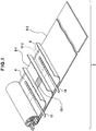
- Fig. 1 shows an example of a capacitor element used for a capacitor according to an embodiment.
- Fig. 1 shows an example of a state, unrolled state, in which the capacitor element is partially opened.
- the capacitor element 2 is, for example, an element of either an electric double layer capacitor or an electrolytic capacitor.
- this capacitor element 2 includes an anode foil 4, a cathode foil 6, and separators 8-1, 8-2.
- an aluminum foil is used for the anode foil 4 and the cathode foil 6, and a dielectric oxide film is formed on the anode foil 4 by a chemical conversion treatment after an etching process.
- the separators 8-1, 8-2 are made of, for example, electrolytic paper such as a kraft fiber nonwoven fabric and a hemp fiber nonwoven fabric, and have an insulation function between the anode foil 4 and the cathode foil 6.
- the separator 8-1 includes an embossed part 10-1
- the separator 8-2 includes an embossed part 10-2.
- the embossed parts 10-1, 10-2 are an example of a low insulation part of the present disclosure, and embossing is performed on the separators 8-1, 8-2 so that the insulation function of the separators 8-1, 8-2 becomes lower as compared to before the embossing. This low insulation part forms a vulnerable part having a low withstand voltage against an overvoltage Vs.
- this vulnerable part has withstand voltage characteristics satisfying the withstand voltage performance required for the capacitor.
- an unevenly-formed roller is pressed against one surface of each of the separators 8-1, 8-2 so that unevenness is formed on the separators 8-1, 8-2 due to a difference in compression.
- the capacitor element 2 is a winding element of the laminated anode foil 4, the cathode foil 6, and the separators 8-1, 8-2.
- the winding element has the anode foil 4 and the cathode foil 6 stacked via the separator 8-1 and the separator 8-2.
- An anode lead terminal 12 is connected to the anode foil 4 and a cathode lead terminal 14 is connected to the cathode foil 6.
- the anode lead terminal 12 and the cathode lead terminal 14 connect the capacitor element 2 to an external circuit such as a power supply circuit.
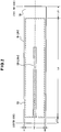
- Fig. 2 shows an example of a formation range of the embossed part.
- Fig. 2 shows an example of the separators 8-1, 8-2 in a unrolled state and it is assumed that a left end is disposed on the center side of the capacitor element 2 while a right end is disposed on the tail end side, i.e., the outer edge side, of the capacitor element 2.
- the embossed parts 10-1, 10-2 are included in the inner part 16.
- the embossed parts 10-1, 10-2 may be arranged in the entire area of the inner part 16 or may be arranged in a portion of the inner part 16.
- the ratio of the heights H1, H2, H3 is set to 5:90:5, for example.
- L1, L2, and L3 denote the length of the outer part 18 on the center side, the length of the inner part 16, and the length of the outer part 18 on the tail end side, respectively
- the ratio of L1, L2, L3 is set to, for example, 5:85:10 in the diametrical direction from the center of the capacitor element 2 in the state of the capacitor element 2, i.e., in the wound state.
- the embossed parts 10-1, 10-2 are arranged within a range of 90 % in a central portion in the height direction of the capacitor element 2 (within a range of 5 to 95 [%] when the upper end is at 0 [%] and the lower end is at 100 [%]), and within a range of 5 to 90 % in the diametrical direction from the center of the capacitor element 2 (within a range of 5 to 90 [%] when the center is at 0 [%] and the tail end is at 100 [%]).
- the arrangement ranges of the embossed parts 10-1, 10-2 may be determined depending on specifications of a capacitor and, for example, a large capacitor having an increased scale of impact may have the outer part 18 enlarged and the inner part 16 reduced, while a small capacitor may have the outer part 18 reduced and the inner part 16 enlarged.
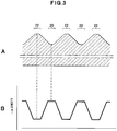
- a of Fig. 3 shows an example of a cross-sectional shape of the embossed part
- B of Fig. 3 shows the density of the embossed part
- Concave parts 20 of the separators 8-1, 8-2 are regions strongly compressed by the roller during embossing, so that the separators 8-1, 8-2 are thinned by compression and the concave parts 20 pull the surrounding electrolytic paper to increase the density of the separators 8-1, 8-2 as shown in B of Fig 3 .
- convex parts 22 of the separators 8-1, 8-2 allow portions of the electrolytic paper to move toward the concave parts 20 to decrease the density as shown in B of Fig. 3 . Since the density of the convex parts 22 becomes lower as compared to before embossing, the insulating function of the separators 8-1, 8-2 decreases. The concave parts 20 and the convex parts 22 form higher and lower density in the separators 8-1, 8-2.
- the basis weight of the separators 8-1, 8-2 rises in the concave parts 20 due to pulling-in of the electrolytic paper while decreasing in the convex parts 22. Therefore, since the basis weight of the convex parts 22 becomes lower as compared to before embossing, the insulation function of the separators 8-1, 8-2 decreases.
- An insulation resistance is formed by the separator 8-1 between the anode foil 4 and the cathode foil 6.
- R1, R2, and R3 denote the insulation resistance of the convex parts 22 of the embossed part 10-1, the insulation resistance of the concave parts 20, and the insulation resistance of the outer part 18 of the separator 8-1, respectively, the insulation resistance R1 of the convex parts 22, whose the density and the basis weight are low, is the smallest.
- the insulation resistances are in the order of R1 ⁇ R3 ⁇ R2. Therefore, when the overvoltage Vs exceeding the rated voltage is applied to the capacitor, a short circuit occurs at the convex parts 22 having the smallest insulation resistance.
- the separator 8-2 Similarly in the separator 8-2, a short circuit occurs at the convex parts 22 having the smallest insulation resistance. Therefore, since the separators 8-1, 8-2 include the low insulation parts because of the formation of the embossed parts 10-1, 10-2, the short circuit between the anode foil 4 and the cathode foil 6 can be guided to the inner part 16 of the capacitor element 2 including the embossed parts 10-1, 10-2. Since the embossed parts 10-1, 10-2 are surrounded by the outer part 18, the impact due to the short circuit is buffered by the outer part 18. In other words, the impact from the capacitor element 2 toward a case is absorbed by the outer part 18 of the capacitor element.
- the insulation resistance R1 of the convex parts 22 is smaller than the insulation resistance R3 of the outer part 18, the short circuit occurs earlier as compared to a non-embossed capacitor element. Therefore, an increase in the movement energy can be suppressed in the capacitor element 2.
- the capacitor element 2 as described above is housed in a case of a capacitor, and the case is sealed with a sealing body such as a sealing plate.
- a sealing body such as a sealing plate.
- This production step is an example of a production method for the capacitor of the present invention.
- the production step for the capacitor includes a step of forming the anode foil 4, a step of forming the cathode foil 6, a step of forming the embossed separators 8-1, 8-2, a step of forming the capacitor element 2, a step of connecting terminals of the capacitor element 2, and a step of enclosing the capacitor element 2.
- the anode foil 4 described above is formed from an aluminum foil, for example. As described above, an etching process is performed on the aluminum foil and a dielectric oxide film is formed on the surface thereof by a chemical conversion treatment, for example.
- the anode lead terminal 12 is connected to the anode foil 4.
- the cathode foil 6 described above is formed from an aluminum foil, for example.
- the cathode lead terminal 14 is connected to the cathode foil 6.
- the embossing described above is performed on a portion or the entire area of the inner part 16 of the separator 8-1 to form the embossed part 10-1.
- the embossing is formed by, for example, pressing an unevenly-formed roller against the electrolytic paper at predetermined timing during the course of feeding that is a course from pulling out the electrolytic paper from a roll with the electrolytic paper to putting the electrolytic paper on the anode foil 4 and the cathode foil 6.
- the embossing may be performed before cutting the electrolytic paper to the size of the separator 8-1, or may be performed after the cutting.
- the separator 8-2 is embossed to form the embossed part 10-2.
- the anode foil 4 and the cathode foil 6 are stacked via the separator 8-1 and the separator 8-2 between the foils, and they are wound to form the capacitor element 2.
- an anode terminal is connected to the anode lead terminal 12 of the capacitor element 2 and a cathode terminal is connected to the cathode lead terminal 14 of the capacitor element 2. It is assumed that the anode terminal and the cathode terminal are attached in advance to the sealing plate. A pressure valve may be attached to the sealing plate so as to discharge a gas generated inside the capacitor to the outside.
- the capacitor element 2 is housed in a case prepared in advance, and the case is sealed with the sealing plate. For this sealing, a curling process is performed on an opening end portion of the case to fix the sealing plate. As a result, the capacitor is completed.
- the present invention is applied to a capacitor in the form of the anode foil 4 and the cathode foil 6 wound with the separators 8-1, 8-2 interposed therebetween.
- the present invention is also applicable to a capacitor in the form of the anode foil and the cathode foil laminated with the separators interposed therebetween.
- the kraft fiber nonwoven fabric is used for the separators 8-1, 8-2.
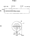
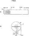
- the separators 8-1, 8-2 include the embossed parts 10-1, 10-2 within the range of 20 [%] in the central portion as shown in A of Fig. 4 in the height direction of the capacitor element 2, and within a range indicated as a processing area 34 in a plane view of the capacitor element 2 shown in B of Fig. 4 , or specifically, within the range of 5 to 65 [%] in the diametrical direction from the center of the capacitor element 2.
- the current flows through the embossed parts 10-1, 10-2 serving as the low insulation part formed inside the capacitor element 2 so that a short circuit is preferentially generated inside the capacitor element 2, and the impact due to the short circuit can be confined in the capacitor element 2 by the anode foil 4, the cathode foil 6, and the separators 8-1, 8-2 that are around the short circuit.
- the hemp fiber nonwoven fabric is used for the separators 8-1, 8-2, and the embossed parts 10-1, 10-2 are arranged at the same positions as Example 1. Even in the capacitor including the capacitor element 2 as described above, the generated overcurrent flows through the embossed parts 10-1, 10-2 so that a short circuit is preferentially generated inside the capacitor element 2 and, therefore, the impact due to the short circuit can be confined in the capacitor element 2 by the anode foil 4, the cathode foil 6, and the separators 8-1, 8-2 that are around the short circuit.
- the kraft fiber nonwoven fabric is used for the separators 8-1, 8-2.
- the separators 8-1, 8-2 include the embossed parts 10-1, 10-2 within the range of 70 [%] in the central portion as shown in A of Fig. 5 in the height direction of the capacitor element 2, and within a range indicated as a processing area 36 in a plane view of the capacitor element 2 shown in B of Fig. 5 , or specifically, within the range of 5 to 25 [%], about 5 to 30 [%], in the diametrical direction from the center of the capacitor element 2.
- the generated overcurrent flows through the embossed parts 10-1, 10-2 so that a short circuit is preferentially generated inside the capacitor element 2 and, therefore, the impact due to the short circuit can be confined in the capacitor element 2 by the anode foil 4, the cathode foil 6, and the separators 8-1, 8-2 that are around the short circuit.
- the hemp fiber nonwoven fabric is used for the separators 8-1, 8-2, and the embossed parts 10-1, 10-2 are arranged at the same positions as Example 3. Even with such a configuration, the same effects as the first to third embodiments can be acquired.
- the processing of the embossed part 10-1 is performed in advance at a predetermined position on electrolytic paper used as the separator 8-1. This processing is performed by, for example, pressing a jig for embossing against a surface portion of the electrolytic paper etc. used as the separator.
- the embossed separator is stored in a rolled state until production of the capacitor element 2, for example.
- the embossed part 10-1 having predetermined width XH and length is formed in the inner part 16 of the flat surface portion of the separator.
- the embossed parts 10-1 having a predetermined length are intermittently formed along a foil longitudinal direction of the anode foil 4 and the cathode foil 6, the length of one of the intermittently formed embossed parts 10-1 is the length L2 used in the one capacitor element 2.
- the length between the embossed parts 10-1 is the sum of the length L1 of the outer part 18 on the center side and the length L3 of the outer part 18 of the tail end portion. This makes it possible to supply the separator in the rolled state continuously to a winding position, so that the capacitor elements 2 can continuously and efficiently be produced.
- the anode foil 4 In a winding process of the capacitor element 2, the anode foil 4, the embossed separator 8-1, the cathode foil 6, and the separator 8-2 are wound in a laminated state.
- the embossed part 10-2 may be formed on a flat surface portion of the separator 8-2.
- the formation position of the embossed part 10-1 for the separator 8-1 can be confirmed in advance and, therefore, the capacitor element 2 can be enhanced in quality and accuracy.
- a formation process of the embossed part 10-1 is performed on the separator 8-1 simultaneously with the winding process of the capacitor element 2.
- a winding device of the capacitor element 2 includes, for example, a roller-shaped jig on an arrangement path of the separator 8-1. This jig contacts the separator 8-1 continuously or at an arbitrary timing during execution of the winding process of the capacitor element 2 so as to form the embossed part 10-1. Depending on the contact timing of this jig, the number and the length of the formed embossed parts 10-1 are determined.
- the width of the embossed part 10-1 with respect to the surface of the separator 8-1 is determined by the width of the jig and the position of contact with the surface of the separator 8-1.
- This embodiment represents the case of forming a single separator by combining a plurality of separators.
- the embossed part 10-1 can be arranged at an arbitrary position.
- the band-shaped embossed part 10-1 is formed in the longitudinal direction at a predetermined height position of the separator 8-1.
- This separator 8-1 is an example of a first separator of the present disclosure.
- the processing of the embossed part 10-1 is performed in the same way as the method described in Example 5.
- the arrangement position of the low insulation part of the separator 8 to the planes of the anode foil 4 and the cathode foil 6 is set in the winding process of the capacitor element 2 and, then the separator 8-1 may form the position of the embossed part 10-1 from the tail end portion side of the electrolytic paper.
- the anode foil 4, a separator 8-3 without an embossed part, the separator 8-1 provided with the embossed part 10-1, the cathode foil 6, and the separator 8-2 are disposed for a winding device of the capacitor element 2.
- the separator 8-3 is an example of the first separator of the present disclosure, and the first separator has a planar or near-planar surface facing a foil surface of the anode foil 4 or the cathode foil 6. This separator 8-3 is combined with the separator 8-1 to form a single separator.
- the separator 8-1 and the separator 8-3 are desirably arranged at adjacent or close positions.
- the separators 8-1, 8-3 may be brought close to each other at the connection position on the arrangement path of the separators.
- the anode foil 4, the separator 8-3, the cathode foil 6, and the separator 8-2 are connected to a winding portion of a production device.
- an end portion 32 of the separator 8-1 is kept on a predetermined arrangement path by a cutting means not shown or a supporting means of a separator.
- the capacitor element 2 is wound with the separator 8-3 from the start of winding until a predetermined timing, for example.
- the separator 8-3 is cut at the predetermined timing.
- the end portion 32 of the separator 8-1 is then connected to an end portion 33 of the separator 8-3 on the side of the wound capacitor element 2 so that they are continuously arranged.
- the embossed part 10-1 serving as the low insulation part is formed in the capacitor element 2.
- the separator 8-1 and the separator 8-3 are connected by using an adhesive material such as an adhesive tape, for example.
- the separator 8-1 and the separator 8-2 may or may not overlap with each other as long as the separators are arranged continuously without intermission. Obviously, this is performed under the condition without occurrence of short circuit.
- the separator 8-1 is cut.
- the end portion 33 of the separator 8-3 is then connected to the end portion 32 of the separator 8-1 on the side of the wound capacitor element 2, and the winding process is resumed as shown in C of Fig. 6 .
- This connection is achieved by using the adhesive tape etc. as described above.
- the separator 8-3 without the embossed part are wound. In this way, the embossed part is prevented from being disposed on the tail end side of the separator, i.e., on the outer circumferential side of the capacitor element 2.
- the order of switching of the separators 8-1, 8-3 is not limited to the case described above.
- the separator 8-1 may be wound first and then switched to the separator 8-3.
- the capacitor element 2 can be formed with the embossed part 10-1 arranged at an arbitrary position.
- overlapping parts 40 are provided between the separators by ensuring a length Lb of the separator 8-1 longer than an arrangement length La of the embossed part 10-1.
- Each overlapping part 40 is a connecting portion between the separator 8-1 and the separator 8-3, and is an example of a connecting part of the present disclosure.
- the length Lc of the overlapping part 40 may arbitrarily be set, and may be set in accordance with the size of the capacitor element 2, the magnitude of tension during the processing, or the usage environment, capacity, and withstand voltage of the capacitor, for example.
- an adhesive material such as an adhesive tape is affixed to cover the overlapping part 40.
- the adhesive tape is a tape made of a material such as polyphenylene sulfide (PPS) or polypropylene (PP), for example.
- PPS polyphenylene sulfide
- PP polypropylene
- the adhesive material a material other than a tape may be used. In this case, the type of the adhesive material is selected in consideration of the influence on an electrolytic solution used for the capacitor.
- Such a configuration can be achieved by adding a separator arrangement line to an existing winding device of a capacitor element and is therefore highly convenient. Since the length of formation of the embossed part 10-1 can arbitrarily be set, the production device can deal with production of various types of capacitors. Since the connection strength can be maintained by providing the overlapping part 40 between the separators, breakage etc. can be prevented from occurring in a portion other than the embossed part.
- capacitors having various embossing positions are prepared for performing an overvoltage application experiment of each of the capacitors.
- the capacitors of Examples 1 to 4 described above and capacitors of Comparative Examples 1 to 3 described below are used.
- the kraft fiber nonwoven fabric is used as separators 108-1, 108-2.
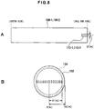
- the separators 108-1, 108-2 include embossed parts 110-1, 110-2 within the range of 20 [%] in the central portion as shown in A of Fig. 8 in the height direction of the capacitor element 102, and within a range indicated as a processing area 134 in a plane view of the capacitor element 102 shown in B of Fig. 8 , or specifically, within the range of 91 to 100 [%] in the diametrical direction from the center of the capacitor element 102.
- the kraft fiber nonwoven fabric is used as the separators 108-1, 108-2.
- the separators 108-1, 108-2 include the embossed parts 110-1, 110-2 within the range of 10 [%] in the upper portion as shown in A of Fig. 9 in the height direction of the capacitor element 102, and within a range indicated as a processing area 136 in a plane view of the capacitor element 102 shown in B of Fig. 9 , or specifically, in the separators 108-1, 108-2 within the range of 5 to 25 [%] in the diametrical direction from the center of the capacitor element 102.
- the kraft fiber nonwoven fabric is used as the separators 108-1, 108-2.
- the separators 108-1, 108-2 include the embossed parts 110-1, 110-2 within the range of 20 [%] in the central portion in the height direction of the capacitor element, and within the range of 0 to 4 [%] in the diametrical direction from the center of the capacitor element 102.
- An overvoltage of 780 [V] is applied to each of the capacitors to cause a short circuit between the anode foil 4 and the cathode foil 6, and the operation of the pressure valve and the damage of at least one of the case or the sealing plate are evaluated.
- the kraft fiber nonwoven fabric or the hemp fiber nonwoven fabric is used as the separators 8-1, 8-2.
- the separators may be those mainly made of natural fibers such as Manila paper and cellulose paper, those mainly made of synthetic fibers, or those mainly made of fibers of glass, synthetic polymer, etc.
- the adhesive material such as the adhesive tape is used for connecting the separator 8-1 and the separator 8-3 in the example described above, the present invention is not limited thereto.
- the separator 8-1 and the separator 8-2 may continuously be arranged by a technique such as ultrasonic connection and cold welding without using an adhesive such as an adhesive tape.
- the low insulation part having the reduced insulation function between the anode foil and the cathode foil is included inside the capacitor element, and an overcurrent flowing between the anode foil and the cathode foil can be made to flow through the low insulation part. Since a short circuit can be caused in the low insulation part at a stage of lower electricity accumulation as compared to a capacitor without this low insulation part, the impact due to overcurrent is smaller, and the anode foil, the cathode foil, and the separator around the low insulation part can confine the impact due to the short circuit within the capacitor element. Since the damage of the case and the sealing member can be reduced or avoided, the reliability of the capacitor can be enhanced.
Landscapes
- Engineering & Computer Science (AREA)
- Power Engineering (AREA)
- Microelectronics & Electronic Packaging (AREA)
- Manufacturing & Machinery (AREA)
- Electric Double-Layer Capacitors Or The Like (AREA)
- Fixed Capacitors And Capacitor Manufacturing Machines (AREA)
Abstract
Description
- A technique of the present disclosure relates to, for example, a capacitor such as an electrolytic capacitor and an electric double layer capacitor, and a production method therefor.
- A capacitor such as an electrolytic capacitor and an electric double layer capacitor is not only used alone but also used in a form of parallel connection or series connection of a plurality of capacitors. By enlarging areas of an anode foil and a cathode foil of a capacitor element in this capacitor, the capacitance of the capacitor can be made higher. Additionally, by selecting a connection form of a plurality of capacitors, a higher capacity and a higher withstand voltage can be achieved as compared to a single capacitor.
- With regard to an anode foil and a cathode foil of a capacitor, it is known that the anode foil is made wider in width than the cathode foil and that the foils are wound with a separator interposed therebetween (e.g., Patent Document 1). In such a capacitor, even if a burr projecting from the anode foil in the width direction thereof breaks through the separator and reaches the cathode foil side, contact with the cathode foil having a width narrower than the anode foil is avoided and a short circuit can be prevented from occurring between the anode foil and the cathode foil due to the burr.
- With regard to a wound form of a capacitor element, a capacitor is known that has a hollow winding part disposed in a winding core part of the capacitor element with the anode foil removed from this hollow winding part (e.g., Patent Document 2) . In such a capacitor, the capacitor element is sealed in a case, so that a pressure of gas filled in the case acts on the capacitor element. Therefore, a buckling force toward a space of the winding core part of the capacitor element is generated by the gas pressure in the vicinity of the winding core part of the capacitor element. The hollow winding part is disposed in the winding core part of the capacitor element to prevent the anode foil from folding due to absorbance of the buckling force and to prevent a short circuit between the anode foil and the cathode foil.
-
- Patent Document 1: Japanese Unexamined Utility Model Application Publication No.
52-037247 - Patent Document 2: Japanese Laid-Open Patent Publication No.
4-361517 - In some cases, an abnormal stress is generated so that an overvoltage Vs etc. exceeding a rated value are applied to a capacitor. For example, if an excessive voltage close to a twofold rated voltage of the capacitor is applied, the anode foil and the cathode foil may be short-circuited due to a leakage current. When a short circuit occurs, a large current flows through the short-circuited position, and a spark is generated by this large current. This spark melts the electrode foils and gasifies electrolyte etc. Although a capacitor including a pressure valve discharges the generated gas through the pressure valve, a rapid rise in internal pressure can cause a rupture etc. of the capacitor. Additionally, when such an abnormal state occurs, a capacitor element with enhanced movement energy may collide with a sealing plate to disrupt the sealing state of the case sealed with the sealing plate and may cause a situation that the capacitor element protrudes out of the case.
- Even if the capacitor has no connection abnormality, an abnormality occurring in an electric circuit including the capacitor may make it impossible to avoid a trouble such as the overvoltage Vs being applied to the capacitor. Therefore, higher safety is required for the capacitor. For example, in a capacitor element in which an anode foil and a cathode foil wound together with a separator interposed between the cathode foil and the anode foil set wider in width than the cathode foil, if an occurrence of an abnormal stress causes a spark due to a short circuit between the anode foil and the cathode foil on the bottom side of the case, the capacitor element may collide with the sealing plate due to a large movement energy. This causes a problem that the sealing state of the case is disrupted and that the capacitor element cannot be prevented from protruding outside from the case.
-
Patent Documents 1 and 2 do not disclose or suggest such a requirement and a problem and do not disclose or suggest a configuration etc. for solving the problem. - In view of the problem, an object of the present invention is to avoid a damage of the case to prevent an abnormal situation such as the capacitor element protruding out of the case when the capacitor falls into an abnormal state.
- To achieved the object, an aspect of a capacitor of the present disclosure provides a capacitor using a capacitor element having an anode foil and a cathode foil wound with a separator interposed between the anode foil and the cathode foil, the separator includes a low insulation part having a low insulation function between the anode foil and the cathode foil, and the low insulation part may be included within a range of 90 % in a central portion in a height direction of the capacitor element and within a range of 5 to 90 % in a diametrical direction from the center of the capacitor element.
- In the capacitor, the separator may have a first separator insulating the anode foil and the cathode foil from each other along a foil longitudinal direction and a second separator including the low insulation part, and the first separator and the second separator may continuously be arranged along the foil longitudinal direction.
- In the capacitor, the low insulation part may have the low insulation function due to the separator of which density or basis weight is low.
- In the capacitor, the separator may include the low insulation part in which an embossed part, a fluted part, or a cut part is formed.
- To achieved the object, an aspect of a production method for a capacitor of the present disclosure comprises the steps of forming an anode foil; forming a cathode foil; forming a low insulation part having a low insulation function in a separator, the low insulation part being between the anode foil and the cathode foil; and stacking the anode foil and the cathode foil via the separator, and forming a capacitor element by winding. The low insulation part may be included within a range of 90 % in a central portion in a height direction of the capacitor element and within a range of 5 to 90 % in a diametrical direction from the center of the capacitor element.
- In the production method for a capacitor, the method may include forming a first separator insulating the anode foil and the cathode foil from each other and a second separator including a low insulation part having a low insulation function between the anode foil and the cathode foil, and continuously arranging the first separator and the second separator along a foil longitudinal direction.
- According to the present invention, any of the following effects is acquired
- (1) When an overvoltage Vs is applied between the anode foil and the cathode foil and an overcurrent flows through the anode foil and the cathode foil, the current preferentially flows through the low insulation part to cause a short circuit between the anode foil and the cathode foil facing across the low insulation part. Since the short circuit is caused at a desired position in the capacitor element, the impact due to the short circuit is confined in the capacitor element. The damage of the case and the sealing plate can be reduced or avoided.
- (2) Abnormalities such as protrusion of the capacitor element from the case can be reduced or avoided.
- Other objects, features, and advantages of the present invention will become more apparent by reference to the accompanying drawings and embodiments.
-
-
Fig. 1 is a diagram of an example of a capacitor element used for a capacitor according to an embodiment. -
Fig. 2 is a diagram of an arrangement position of an embossed part. -
Fig. 3 is a diagram of an example of a cross-sectional shape and density of the embossed part. -
Fig. 4 is a diagram of an arrangement position of embossed parts of capacitors according to Examples 1 and 2. -
Fig. 5 is a diagram of arrangement positions of embossed parts of capacitors according to Examples 3 and 4. -
Fig. 6 is a diagram of a production process example of the capacitor element. -
Fig. 7 is a diagram of a configuration example of a separator. -
Fig. 8 is a diagram of an arrangement position of an embossed part of a capacitor according to Comparative Example 2. -
Fig. 9 is a diagram of an arrangement position of an embossed part of a capacitor according to Comparative Example 3. -
Fig. 1 shows an example of a capacitor element used for a capacitor according to an embodiment.Fig. 1 shows an example of a state, unrolled state, in which the capacitor element is partially opened. Thecapacitor element 2 is, for example, an element of either an electric double layer capacitor or an electrolytic capacitor. By way of example, thiscapacitor element 2 includes an anode foil 4, acathode foil 6, and separators 8-1, 8-2. - For example, an aluminum foil is used for the anode foil 4 and the
cathode foil 6, and a dielectric oxide film is formed on the anode foil 4 by a chemical conversion treatment after an etching process. - The separators 8-1, 8-2 are made of, for example, electrolytic paper such as a kraft fiber nonwoven fabric and a hemp fiber nonwoven fabric, and have an insulation function between the anode foil 4 and the
cathode foil 6. The separator 8-1 includes an embossed part 10-1, and the separator 8-2 includes an embossed part 10-2. The embossed parts 10-1, 10-2 are an example of a low insulation part of the present disclosure, and embossing is performed on the separators 8-1, 8-2 so that the insulation function of the separators 8-1, 8-2 becomes lower as compared to before the embossing. This low insulation part forms a vulnerable part having a low withstand voltage against an overvoltage Vs. Obviously, even this vulnerable part has withstand voltage characteristics satisfying the withstand voltage performance required for the capacitor. In this embossing, for example, an unevenly-formed roller is pressed against one surface of each of the separators 8-1, 8-2 so that unevenness is formed on the separators 8-1, 8-2 due to a difference in compression. - For example, the
capacitor element 2 is a winding element of the laminated anode foil 4, thecathode foil 6, and the separators 8-1, 8-2. The winding element has the anode foil 4 and thecathode foil 6 stacked via the separator 8-1 and the separator 8-2. - An
anode lead terminal 12 is connected to the anode foil 4 and acathode lead terminal 14 is connected to thecathode foil 6. Theanode lead terminal 12 and thecathode lead terminal 14 connect thecapacitor element 2 to an external circuit such as a power supply circuit. -
Fig. 2 shows an example of a formation range of the embossed part.Fig. 2 shows an example of the separators 8-1, 8-2 in a unrolled state and it is assumed that a left end is disposed on the center side of thecapacitor element 2 while a right end is disposed on the tail end side, i.e., the outer edge side, of thecapacitor element 2. - Assuming that flat surface portions of the separators is divided into an
inner part 16 and anouter part 18 in the separators 8-1, 8-2 in such a unrolled state, the embossed parts 10-1, 10-2 are included in theinner part 16. The embossed parts 10-1, 10-2 may be arranged in the entire area of theinner part 16 or may be arranged in a portion of theinner part 16. - When H1, H2, and H3 denote the height of the
outer part 18 on the upper side, the height of theinner part 16, and the height of theouter part 18 on the lower side, respectively, the ratio of the heights H1, H2, H3 is set to 5:90:5, for example. When L1, L2, and L3 denote the length of theouter part 18 on the center side, the length of theinner part 16, and the length of theouter part 18 on the tail end side, respectively, the ratio of L1, L2, L3 is set to, for example, 5:85:10 in the diametrical direction from the center of thecapacitor element 2 in the state of thecapacitor element 2, i.e., in the wound state. Therefore, the embossed parts 10-1, 10-2 are arranged within a range of 90 % in a central portion in the height direction of the capacitor element 2 (within a range of 5 to 95 [%] when the upper end is at 0 [%] and the lower end is at 100 [%]), and within a range of 5 to 90 % in the diametrical direction from the center of the capacitor element 2 (within a range of 5 to 90 [%] when the center is at 0 [%] and the tail end is at 100 [%]). The arrangement ranges of the embossed parts 10-1, 10-2 may be determined depending on specifications of a capacitor and, for example, a large capacitor having an increased scale of impact may have theouter part 18 enlarged and theinner part 16 reduced, while a small capacitor may have theouter part 18 reduced and theinner part 16 enlarged. - A of
Fig. 3 shows an example of a cross-sectional shape of the embossed part, and B ofFig. 3 shows the density of the embossed part. -
Concave parts 20 of the separators 8-1, 8-2 are regions strongly compressed by the roller during embossing, so that the separators 8-1, 8-2 are thinned by compression and theconcave parts 20 pull the surrounding electrolytic paper to increase the density of the separators 8-1, 8-2 as shown in B ofFig 3 . - In contrast,
convex parts 22 of the separators 8-1, 8-2 allow portions of the electrolytic paper to move toward theconcave parts 20 to decrease the density as shown in B ofFig. 3 . Since the density of theconvex parts 22 becomes lower as compared to before embossing, the insulating function of the separators 8-1, 8-2 decreases. Theconcave parts 20 and theconvex parts 22 form higher and lower density in the separators 8-1, 8-2. - As is the case with the density, the basis weight of the separators 8-1, 8-2 rises in the
concave parts 20 due to pulling-in of the electrolytic paper while decreasing in theconvex parts 22. Therefore, since the basis weight of theconvex parts 22 becomes lower as compared to before embossing, the insulation function of the separators 8-1, 8-2 decreases. - An insulation resistance is formed by the separator 8-1 between the anode foil 4 and the
cathode foil 6. When R1, R2, and R3 denote the insulation resistance of theconvex parts 22 of the embossed part 10-1, the insulation resistance of theconcave parts 20, and the insulation resistance of theouter part 18 of the separator 8-1, respectively, the insulation resistance R1 of theconvex parts 22, whose the density and the basis weight are low, is the smallest. The insulation resistances are in the order of R1<R3<R2. Therefore, when the overvoltage Vs exceeding the rated voltage is applied to the capacitor, a short circuit occurs at theconvex parts 22 having the smallest insulation resistance. Similarly in the separator 8-2, a short circuit occurs at theconvex parts 22 having the smallest insulation resistance. Therefore, since the separators 8-1, 8-2 include the low insulation parts because of the formation of the embossed parts 10-1, 10-2, the short circuit between the anode foil 4 and thecathode foil 6 can be guided to theinner part 16 of thecapacitor element 2 including the embossed parts 10-1, 10-2. Since the embossed parts 10-1, 10-2 are surrounded by theouter part 18, the impact due to the short circuit is buffered by theouter part 18. In other words, the impact from thecapacitor element 2 toward a case is absorbed by theouter part 18 of the capacitor element. Furthermore, since the insulation resistance R1 of theconvex parts 22 is smaller than the insulation resistance R3 of theouter part 18, the short circuit occurs earlier as compared to a non-embossed capacitor element. Therefore, an increase in the movement energy can be suppressed in thecapacitor element 2. - The
capacitor element 2 as described above is housed in a case of a capacitor, and the case is sealed with a sealing body such as a sealing plate. In such a capacitor, the impact due to the short circuit applied to the case or the sealing plate is reduced, and the damage caused by the occurrence of the short circuit is confined in the capacitor, so that the destruction of the case and the sealing plate is avoided. - This production step is an example of a production method for the capacitor of the present invention.
- The production step for the capacitor includes a step of forming the anode foil 4, a step of forming the
cathode foil 6, a step of forming the embossed separators 8-1, 8-2, a step of forming thecapacitor element 2, a step of connecting terminals of thecapacitor element 2, and a step of enclosing thecapacitor element 2. - At the step of forming the anode foil 4, the anode foil 4 described above is formed from an aluminum foil, for example. As described above, an etching process is performed on the aluminum foil and a dielectric oxide film is formed on the surface thereof by a chemical conversion treatment, for example. The
anode lead terminal 12 is connected to the anode foil 4. - At the step of forming the
cathode foil 6, thecathode foil 6 described above is formed from an aluminum foil, for example. Thecathode lead terminal 14 is connected to thecathode foil 6. - At the step of forming the embossed separators 8-1, 8-2, the embossing described above is performed on a portion or the entire area of the
inner part 16 of the separator 8-1 to form the embossed part 10-1. The embossing is formed by, for example, pressing an unevenly-formed roller against the electrolytic paper at predetermined timing during the course of feeding that is a course from pulling out the electrolytic paper from a roll with the electrolytic paper to putting the electrolytic paper on the anode foil 4 and thecathode foil 6. The embossing may be performed before cutting the electrolytic paper to the size of the separator 8-1, or may be performed after the cutting. As is the case with the separator 8-1, the separator 8-2 is embossed to form the embossed part 10-2. - At the step of forming the
capacitor element 2, for example, the anode foil 4 and thecathode foil 6 are stacked via the separator 8-1 and the separator 8-2 between the foils, and they are wound to form thecapacitor element 2. - At the step of connecting terminals of the
capacitor element 2, an anode terminal is connected to theanode lead terminal 12 of thecapacitor element 2 and a cathode terminal is connected to thecathode lead terminal 14 of thecapacitor element 2. It is assumed that the anode terminal and the cathode terminal are attached in advance to the sealing plate. A pressure valve may be attached to the sealing plate so as to discharge a gas generated inside the capacitor to the outside. - At the step of enclosing, the
capacitor element 2 is housed in a case prepared in advance, and the case is sealed with the sealing plate. For this sealing, a curling process is performed on an opening end portion of the case to fix the sealing plate. As a result, the capacitor is completed. - According to the capacitor according to this embodiment, the following effects can be acquired.
- (1) Since the capacitor can prevent a short circuit in the
outer part 18 of thecapacitor element 2 when the overvoltage Vs exceeding the rated voltage acts between the terminals, the safety is enhanced and the reliability can be improved. - (2) When the overvoltage Vs exceeding the rated voltage is applied between the anode terminal and the cathode terminal and an overcurrent flows between the anode foil 4 and the
cathode foil 6, a short-circuit position is guided to theinner part 16 of thecapacitor element 2, and the impact due to the short circuit is preferentially generated in theinner part 16 of thecapacitor element 2 and thereby can be buffered in theouter part 18. Consequently, the damage of the case and the sealing plate can be suppressed. - (3) The short circuit occurs at a stage of lower electricity accumulation as compared to capacitors without embossed parts 10-1, 10-2. Therefore, an amount of overcurrent flowing between the anode foil 4 and the
cathode foil 6 becomes smaller, and the impact can be suppressed. - (4) Since the increase in the movement energy of the
capacitor element 2 can be suppressed, the collision of thecapacitor element 2 against the sealing plate and the destruction of the case and the sealing plate can be prevented, and thecapacitor element 2 can be prevented from protruding out of the case. -
- (1) In the embodiment, the embossed parts 10-1, 10-2 are arranged within the range of 90 % in the central portion in the height direction of the
capacitor element 2 and within the range of 5 to 90 % in the diametrical direction from the center of thecapacitor element 2. However, the arrangement range of the embossed parts 10-1, 10-2 is preferably further limited to the inner side of thecapacitor element 2. For example, preferably, the ratio of the heights H1, H2, H3 is set to 15:70:15 so that the embossed parts 10-1, 10-2 are within the range of 70 % in the central portion in the height direction of thecapacitor element 2 and, preferably, the ratio of L1, L2, L3 is set to 5:60:35 in the diametrical direction from the center of thecapacitor element 2 so that the embossed parts 10-1, 10-2 are within the range of 5 to 65 % in the diametrical direction from the center of thecapacitor element 2. Since the arrangement range of the embossed parts 10-1, 10-2 is further limited to the inner side of thecapacitor element 2, the short-circuit position can further be guided to the inner side of thecapacitor element 2. - (2) Although the embossing is performed on each of the two separators 8-1, 8-2 in the embodiment, either one of the separators may include the embossed part. Alternatively, the embossed part 10-1 of the separator 8-1 may be disposed at a position different from the embossed part 10-2 of the separator 8-2.
- (3) Although the embossing is performed on one surface of each of the separators 8-1, 8-2 in the embodiment, the embossing may be performed on both surfaces . When the embossing is performed on one surface, it is not necessary to synchronize with embossing on the opposite surface side. When the embossing is performed on both surfaces, a difference between the higher and lower densities can be increased by making the concave parts formed on the respective surfaces opposite to each other and making the convex parts opposite to each other.
- (4) In the embodiment, the embossing is performed on the separators 8-1, 8-2 to achieve the low insulation parts in which low-density low-basis-weight parts are formed by including the embossed parts 10-1, 10-2. However, for example, the capacitor may include fluted parts on which grooving by fluting is performed, or cut parts having the low insulation parts formed by cutting the surfaces of the separators 8-1, 8-2. The density or the basis weight of the separators 8-1, 8-2 can be lowered also by the fluted parts or the cut parts formed by cutting the surfaces, and the insulation function can be reduced.
- (5) In the embodiment, the embossing is performed on the separators 8-1, 8-2 to include the low insulation parts between the anode foil 4 and the
cathode foil 6. However, two or more separators may be inserted between electrodes and a through-hole may be formed in one of the separators to form a relatively lower insulation part than the surroundings. - (6) Although a plurality of the separators 8-1, 8-2 is used in the embodiment, the capacitor may have a structure in which only one separator is interposed between the anode foil 4 and the
cathode foil 6. - In the embodiment, the present invention is applied to a capacitor in the form of the anode foil 4 and the
cathode foil 6 wound with the separators 8-1, 8-2 interposed therebetween. However, the present invention is also applicable to a capacitor in the form of the anode foil and the cathode foil laminated with the separators interposed therebetween. - In the
capacitor element 2 of the capacitor according to Example 1, the kraft fiber nonwoven fabric is used for the separators 8-1, 8-2. The separators 8-1, 8-2 include the embossed parts 10-1, 10-2 within the range of 20 [%] in the central portion as shown in A ofFig. 4 in the height direction of thecapacitor element 2, and within a range indicated as aprocessing area 34 in a plane view of thecapacitor element 2 shown in B ofFig. 4 , or specifically, within the range of 5 to 65 [%] in the diametrical direction from the center of thecapacitor element 2. If an overcurrent is applied to a capacitor including thecapacitor element 2 as described above, the current flows through the embossed parts 10-1, 10-2 serving as the low insulation part formed inside thecapacitor element 2 so that a short circuit is preferentially generated inside thecapacitor element 2, and the impact due to the short circuit can be confined in thecapacitor element 2 by the anode foil 4, thecathode foil 6, and the separators 8-1, 8-2 that are around the short circuit. - In the
capacitor element 2 of the capacitor according to Example 2, the hemp fiber nonwoven fabric is used for the separators 8-1, 8-2, and the embossed parts 10-1, 10-2 are arranged at the same positions as Example 1. Even in the capacitor including thecapacitor element 2 as described above, the generated overcurrent flows through the embossed parts 10-1, 10-2 so that a short circuit is preferentially generated inside thecapacitor element 2 and, therefore, the impact due to the short circuit can be confined in thecapacitor element 2 by the anode foil 4, thecathode foil 6, and the separators 8-1, 8-2 that are around the short circuit. - In the
capacitor element 2 of the capacitor according to Example 3, the kraft fiber nonwoven fabric is used for the separators 8-1, 8-2. The separators 8-1, 8-2 include the embossed parts 10-1, 10-2 within the range of 70 [%] in the central portion as shown in A ofFig. 5 in the height direction of thecapacitor element 2, and within a range indicated as aprocessing area 36 in a plane view of thecapacitor element 2 shown in B ofFig. 5 , or specifically, within the range of 5 to 25 [%], about 5 to 30 [%], in the diametrical direction from the center of thecapacitor element 2. Even in the capacitor including thecapacitor element 2 as described above, the generated overcurrent flows through the embossed parts 10-1, 10-2 so that a short circuit is preferentially generated inside thecapacitor element 2 and, therefore, the impact due to the short circuit can be confined in thecapacitor element 2 by the anode foil 4, thecathode foil 6, and the separators 8-1, 8-2 that are around the short circuit. - In the
capacitor element 2 of the capacitor according to Example 4, the hemp fiber nonwoven fabric is used for the separators 8-1, 8-2, and the embossed parts 10-1, 10-2 are arranged at the same positions as Example 3. Even with such a configuration, the same effects as the first to third embodiments can be acquired. - An example of a production process of a capacitor including processing of separators will be described.
- In the production process of the
capacitor element 2 described in this example, the processing of the embossed part 10-1 is performed in advance at a predetermined position on electrolytic paper used as the separator 8-1. This processing is performed by, for example, pressing a jig for embossing against a surface portion of the electrolytic paper etc. used as the separator. The embossed separator is stored in a rolled state until production of thecapacitor element 2, for example. - The embossed part 10-1 having predetermined width XH and length is formed in the
inner part 16 of the flat surface portion of the separator. For example, if the embossed parts 10-1 having a predetermined length are intermittently formed along a foil longitudinal direction of the anode foil 4 and thecathode foil 6, the length of one of the intermittently formed embossed parts 10-1 is the length L2 used in the onecapacitor element 2. The length between the embossed parts 10-1 is the sum of the length L1 of theouter part 18 on the center side and the length L3 of theouter part 18 of the tail end portion. This makes it possible to supply the separator in the rolled state continuously to a winding position, so that thecapacitor elements 2 can continuously and efficiently be produced. - In a winding process of the
capacitor element 2, the anode foil 4, the embossed separator 8-1, thecathode foil 6, and the separator 8-2 are wound in a laminated state. - Although the case of the separator 8-2 without the embossed part has been described, this is not a limitation. The embossed part 10-2 may be formed on a flat surface portion of the separator 8-2.
- With such a configuration, the formation position of the embossed part 10-1 for the separator 8-1 can be confirmed in advance and, therefore, the
capacitor element 2 can be enhanced in quality and accuracy. - In this embodiment, a formation process of the embossed part 10-1 is performed on the separator 8-1 simultaneously with the winding process of the
capacitor element 2. A winding device of thecapacitor element 2 includes, for example, a roller-shaped jig on an arrangement path of the separator 8-1. This jig contacts the separator 8-1 continuously or at an arbitrary timing during execution of the winding process of thecapacitor element 2 so as to form the embossed part 10-1. Depending on the contact timing of this jig, the number and the length of the formed embossed parts 10-1 are determined. - The width of the embossed part 10-1 with respect to the surface of the separator 8-1 is determined by the width of the jig and the position of contact with the surface of the separator 8-1.
- With such a configuration, since the winding process and the embossing can be performed at the same time, an increase in work procedures can be prevented and the production process can be speeded up.
- This embodiment represents the case of forming a single separator by combining a plurality of separators. As a result, the embossed part 10-1 can be arranged at an arbitrary position.
- In the production process of the
capacitor element 2, first, the band-shaped embossed part 10-1 is formed in the longitudinal direction at a predetermined height position of the separator 8-1. This separator 8-1 is an example of a first separator of the present disclosure. The processing of the embossed part 10-1 is performed in the same way as the method described in Example 5. In the production method for the capacitor described in this example, the arrangement position of the low insulation part of the separator 8 to the planes of the anode foil 4 and thecathode foil 6 is set in the winding process of thecapacitor element 2 and, then the separator 8-1 may form the position of the embossed part 10-1 from the tail end portion side of the electrolytic paper. - In the winding process of the
capacitor element 2, for example, as shown inFig. 6 , the anode foil 4, a separator 8-3 without an embossed part, the separator 8-1 provided with the embossed part 10-1, thecathode foil 6, and the separator 8-2 are disposed for a winding device of thecapacitor element 2. The separator 8-3 is an example of the first separator of the present disclosure, and the first separator has a planar or near-planar surface facing a foil surface of the anode foil 4 or thecathode foil 6. This separator 8-3 is combined with the separator 8-1 to form a single separator. - In the winding process device, the separator 8-1 and the separator 8-3 are desirably arranged at adjacent or close positions. The separators 8-1, 8-3 may be brought close to each other at the connection position on the arrangement path of the separators.
- At the production step of the
capacitor element 2, for example, as shown in A ofFig. 6 , the anode foil 4, the separator 8-3, thecathode foil 6, and the separator 8-2 are connected to a winding portion of a production device. In this state, anend portion 32 of the separator 8-1 is kept on a predetermined arrangement path by a cutting means not shown or a supporting means of a separator. - The
capacitor element 2 is wound with the separator 8-3 from the start of winding until a predetermined timing, for example. In the winding process of thecapacitor element 2, for example, as shown in B ofFig. 6 , the separator 8-3 is cut at the predetermined timing. Theend portion 32 of the separator 8-1 is then connected to anend portion 33 of the separator 8-3 on the side of thewound capacitor element 2 so that they are continuously arranged. By winding the separator 8-1 from this state, the embossed part 10-1 serving as the low insulation part is formed in thecapacitor element 2. The separator 8-1 and the separator 8-3 are connected by using an adhesive material such as an adhesive tape, for example. With regard to "continuously" in this case, the separator 8-1 and the separator 8-2 may or may not overlap with each other as long as the separators are arranged continuously without intermission. Obviously, this is performed under the condition without occurrence of short circuit. - When the connection of the separator 8-1 is completed, the winding of the
capacitor element 2 is resumed, and the winding process is executed until the next set timing. - At the predetermined timing, the separator 8-1 is cut. The
end portion 33 of the separator 8-3 is then connected to theend portion 32 of the separator 8-1 on the side of thewound capacitor element 2, and the winding process is resumed as shown in C ofFig. 6 . This connection is achieved by using the adhesive tape etc. as described above. - In the winding process of the
capacitor element 2, for example, when the winding process approaches the end based on the set winding length of the anode foil 4 and thecathode foil 6, the separator 8-3 without the embossed part are wound. In this way, the embossed part is prevented from being disposed on the tail end side of the separator, i.e., on the outer circumferential side of thecapacitor element 2. The order of switching of the separators 8-1, 8-3 is not limited to the case described above. To form the embossed part 10-1 on the winding core side of thecapacitor element 2, the separator 8-1 may be wound first and then switched to the separator 8-3. - By alternately combining the two types of the separators 8-1, 8-3, as shown in
Fig. 7 , thecapacitor element 2 can be formed with the embossed part 10-1 arranged at an arbitrary position. In the connection between theend portion 32 of the separator 8-1 and theend portion 33 of the separator 8-3, for example, overlappingparts 40 are provided between the separators by ensuring a length Lb of the separator 8-1 longer than an arrangement length La of the embossed part 10-1. Each overlappingpart 40 is a connecting portion between the separator 8-1 and the separator 8-3, and is an example of a connecting part of the present disclosure. The length Lc of the overlappingpart 40 may arbitrarily be set, and may be set in accordance with the size of thecapacitor element 2, the magnitude of tension during the processing, or the usage environment, capacity, and withstand voltage of the capacitor, for example. - For connection between the separator 8-1 and the separator 8-3, for example, an adhesive material such as an adhesive tape is affixed to cover the overlapping
part 40. The adhesive tape is a tape made of a material such as polyphenylene sulfide (PPS) or polypropylene (PP), for example. For the adhesive material, a material other than a tape may be used. In this case, the type of the adhesive material is selected in consideration of the influence on an electrolytic solution used for the capacitor. - Such a configuration can be achieved by adding a separator arrangement line to an existing winding device of a capacitor element and is therefore highly convenient. Since the length of formation of the embossed part 10-1 can arbitrarily be set, the production device can deal with production of various types of capacitors. Since the connection strength can be maintained by providing the overlapping
part 40 between the separators, breakage etc. can be prevented from occurring in a portion other than the embossed part. - By using the kraft fiber nonwoven fabric or the hemp fiber nonwoven fabric for the separators 8-1, 8-2, capacitors having various embossing positions are prepared for performing an overvoltage application experiment of each of the capacitors. For the experiments, the capacitors of Examples 1 to 4 described above and capacitors of Comparative Examples 1 to 3 described below are used.
- In Comparative Example 1, a capacitor is formed without embossing on any of the separators 8-1, 8-2.
- In a
capacitor element 102 of the capacitor according to Comparative Example 2, the kraft fiber nonwoven fabric is used as separators 108-1, 108-2. The separators 108-1, 108-2 include embossed parts 110-1, 110-2 within the range of 20 [%] in the central portion as shown in A ofFig. 8 in the height direction of thecapacitor element 102, and within a range indicated as aprocessing area 134 in a plane view of thecapacitor element 102 shown in B ofFig. 8 , or specifically, within the range of 91 to 100 [%] in the diametrical direction from the center of thecapacitor element 102. - In the
capacitor element 102 of the capacitor according to Comparative Example 3, the kraft fiber nonwoven fabric is used as the separators 108-1, 108-2. The separators 108-1, 108-2 include the embossed parts 110-1, 110-2 within the range of 10 [%] in the upper portion as shown in A ofFig. 9 in the height direction of thecapacitor element 102, and within a range indicated as aprocessing area 136 in a plane view of thecapacitor element 102 shown in B ofFig. 9 , or specifically, in the separators 108-1, 108-2 within the range of 5 to 25 [%] in the diametrical direction from the center of thecapacitor element 102. - In the
capacitor element 102 of the capacitor according to Comparative Example 4, the kraft fiber nonwoven fabric is used as the separators 108-1, 108-2. The separators 108-1, 108-2 include the embossed parts 110-1, 110-2 within the range of 20 [%] in the central portion in the height direction of the capacitor element, and within the range of 0 to 4 [%] in the diametrical direction from the center of thecapacitor element 102. - The capacitors of Examples 1 to 4 and the capacitors of Comparative Examples 1 to 4 are used for the experiments. These capacitors have the following specifications:
- Rated voltage: 400 [V];
- Electrostatic capacity: 5600 [µF];
- Dimensions: (Diameter Φ) 76.2 [mm], (Length L) 130 [mm]; and
- Other: a pressure valve is disposed on a sealing plate.
- An overvoltage of 780 [V] is applied to each of the capacitors to cause a short circuit between the anode foil 4 and the
cathode foil 6, and the operation of the pressure valve and the damage of at least one of the case or the sealing plate are evaluated. - The pressure valve operated in all the capacitors of Examples 1 to 4; however, no damage was confirmed in the case or the sealing plate. In all the
capacitor elements 2, the short circuit occurred in the embossed parts 10-1, 10-2. - In the capacitors of Comparative Example 1, four capacitors out of the five tested capacitors were damaged in the case or the sealing plate. The occurrence locations of the short circuits were not limited to a certain range and were different depending on the
capacitor elements 102. - In the capacitors of Comparative Example 2, the short circuits occurred in the outer circumferential portions of the
capacitor elements 102. Because of the absence of the outer parts of thecapacitor elements 102 absorbing the impacts due to the short circuits, the impacts reached toward the cases, and damage of the cases or the sealing plates of all the capacitors got damaged. - In the capacitors of Comparative Example 3, the short circuits occurred in the upper end portions of the
capacitor elements 102. Because of the absence of the outer parts of thecapacitor elements 102 absorbing the impacts due to the short circuits, the impacts reached toward the cases and the sealing plates, and the cases or the sealing plates of all the capacitors got damaged. - In the capacitors of Comparative Example 4, the short circuits occurred on the center sides of the
capacitor elements 102. Center portions of thecapacitor elements 102 have spaces formed by pulling out a winding shaft used for winding thecapacitor elements 102. Since the short circuits occurred near these spaces, the impacts due to the short circuits reached through the spaces in the center portions of thecapacitor elements 102 toward the sealing plates and the bottom surfaces of the cases, and the cases or the sealing plates of the capacitors got damaged. - The evaluation results are as described in Table 1 below.
[Table 1] valve operation incidence rate of damage in at least one of exterior case or sealing plate Example 1 100 [%] 0 [%] Example 2 100 [%] 0 [%] Example 3 100 [%] 0 [%] Example 4 100 [%] 0 [%] Comparative Example 1 100 [%] 80 [%] break down: exterior case damage 50 [%] sealing plate damage 50 [%] Comparative Example 2 100 [%] 100 [%] break down: exterior case damage 100 [%] Comparative Example 3 100 [%] 100 [%] break down: exterior case damage 60 [%] sealing plate damage 40 [%] Comparative Example 4 100 [%] 80 [%] break down: exterior case damage 50 [%] sealing plate damage 50 [%] - In the embodiments, Examples, and Comparative Examples described above, the kraft fiber nonwoven fabric or the hemp fiber nonwoven fabric is used as the separators 8-1, 8-2. However, the present invention is not limited thereto, and the separators may be those mainly made of natural fibers such as Manila paper and cellulose paper, those mainly made of synthetic fibers, or those mainly made of fibers of glass, synthetic polymer, etc.
- Although the adhesive material such as the adhesive tape is used for connecting the separator 8-1 and the separator 8-3 in the example described above, the present invention is not limited thereto. The separator 8-1 and the separator 8-2 may continuously be arranged by a technique such as ultrasonic connection and cold welding without using an adhesive such as an adhesive tape.
- As described above, the preferable embodiments etc. of the present invention have been described. However, the present invention is not limited to the above description and can obviously variously be modified and altered by those skilled in the art based on the gist of the invention described in claims or disclosed in the description, and it is needless to say that these modifications and alterations fall within the scope of the present invention.
- According to the capacitor and the production method therefor of the present invention, the low insulation part having the reduced insulation function between the anode foil and the cathode foil is included inside the capacitor element, and an overcurrent flowing between the anode foil and the cathode foil can be made to flow through the low insulation part. Since a short circuit can be caused in the low insulation part at a stage of lower electricity accumulation as compared to a capacitor without this low insulation part, the impact due to overcurrent is smaller, and the anode foil, the cathode foil, and the separator around the low insulation part can confine the impact due to the short circuit within the capacitor element. Since the damage of the case and the sealing member can be reduced or avoided, the reliability of the capacitor can be enhanced.
-
- 2
- capacitor element
- 4
- anode foil
- 6
- cathode foil
- 8-1, 8-2
- separator
- 10-1, 10-2
- embossed part
- 12
- anode lead terminal
- 14
- cathode lead terminal
- 16
- inner part
- 18
- outer part
- 20
- concave part
- 22
- convex part
- 30
- jig
- 32, 33
- end portion
- 40
- overlapping part
Claims (6)
- A capacitor using a capacitor element having an anode foil and a cathode foil wound with a separator interposed between the anode foil and the cathode foil, wherein
the separator includes a low insulation part having a low insulation function between the anode foil and the cathode foil, and wherein
the low insulation part is included within a range of 90 % in a central portion in a height direction of the capacitor element and within a range of 5 to 90 % in a diametrical direction from the center of the capacitor element. - The capacitor according to claim 1, wherein
the separator includes:a first separator insulating the anode foil and the cathode foil from each other along a foil longitudinal direction, anda second separator including the low insulation part, and whereinthe first separator and the second separator are continuously arranged along the foil longitudinal direction. - The capacitor according to claim 1 or 2, wherein the low insulation part has the low insulation function due to the separator of which density or basis weight is low.
- The capacitor according to claims 1 to 3, wherein the separator includes the low insulation part in which an embossed part, a fluted part, or a cut part is formed.
- A production method for a capacitor comprising the steps of:forming an anode foil;forming a cathode foil;forming a low insulation part having a low insulation function in a separator, the low insulation part being between the anode foil and the cathode foil; andstacking the anode foil and the cathode foil via the separator, and forming a capacitor element by winding, whereinthe low insulation part is included within a range of 90 % in a central portion in a height direction of the capacitor element and within a range of 5 to 90 % in a diametrical direction from the center of the capacitor element.
- The production method for a capacitor according to claim 5, wherein
the method includes a process of forming a first separator insulating the anode foil and the cathode foil from each other and a second separator including a low insulation part having a low insulation function between the anode foil and the cathode foil, and
continuously arranging the first separator and the second separator along a foil longitudinal direction.
Applications Claiming Priority (2)
| Application Number | Priority Date | Filing Date | Title |
|---|---|---|---|
| JP2015068717 | 2015-03-30 | ||
| PCT/JP2016/001634 WO2016157823A1 (en) | 2015-03-30 | 2016-03-22 | Capacitor and production method therefor |
Publications (2)
| Publication Number | Publication Date |
|---|---|
| EP3279910A1 true EP3279910A1 (en) | 2018-02-07 |
| EP3279910A4 EP3279910A4 (en) | 2018-12-12 |
Family
ID=57006631
Family Applications (1)
| Application Number | Title | Priority Date | Filing Date |
|---|---|---|---|
| EP16771716.4A Withdrawn EP3279910A4 (en) | 2015-03-30 | 2016-03-22 | Capacitor and production method therefor |
Country Status (5)
| Country | Link |
|---|---|
| US (1) | US20180005768A1 (en) |
| EP (1) | EP3279910A4 (en) |
| JP (1) | JP6702309B2 (en) |
| CN (1) | CN107408463B (en) |
| WO (1) | WO2016157823A1 (en) |
Cited By (2)
| Publication number | Priority date | Publication date | Assignee | Title |
|---|---|---|---|---|
| CN111868862A (en) * | 2018-03-27 | 2020-10-30 | Tdk电子股份有限公司 | Capacitor and method for manufacturing capacitor |
| US11631546B2 (en) | 2018-03-27 | 2023-04-18 | Tdk Electronics Ag | Capacitor and method for producing a capacitor |
Families Citing this family (3)
| Publication number | Priority date | Publication date | Assignee | Title |
|---|---|---|---|---|
| JP6816395B2 (en) * | 2016-07-08 | 2021-01-20 | 日本ケミコン株式会社 | Electric double layer capacitor |
| JP6809308B2 (en) * | 2017-03-14 | 2021-01-06 | 日本ケミコン株式会社 | Capacitor device |
| EP4293693A4 (en) * | 2021-02-09 | 2025-06-11 | Nippon Chemi-Con Corporation | CAPACITOR |
Family Cites Families (11)
| Publication number | Priority date | Publication date | Assignee | Title |
|---|---|---|---|---|
| JPS60231318A (en) * | 1984-04-27 | 1985-11-16 | 松下電器産業株式会社 | Aluminum electrolytic condenser |
| JPH025878U (en) * | 1988-06-27 | 1990-01-16 | ||
| JPH10144283A (en) * | 1996-11-12 | 1998-05-29 | Japan Storage Battery Co Ltd | Cylindrical sealed lead-acid battery |
| JP2000164467A (en) * | 1998-11-20 | 2000-06-16 | Nippon Chemicon Corp | Electrolytic capacitor |
| DE10333550B4 (en) * | 2003-07-23 | 2006-06-14 | Epcos Ag | Electrochemical double-layer capacitor and method for impregnating a double-layer capacitor |
| JP2009021491A (en) * | 2007-07-13 | 2009-01-29 | Hitachi Aic Inc | Aluminum electrolytic capacitor |
| JP2009064958A (en) * | 2007-09-06 | 2009-03-26 | Hitachi Aic Inc | Aluminum electrolytic capacitor |
| JP2011192784A (en) * | 2010-03-15 | 2011-09-29 | Jm Energy Corp | Lithium ion capacitor |
| CN104321843B (en) * | 2012-02-21 | 2018-03-02 | 日本贵弥功株式会社 | Electrolytic capacitor |
| JP5076034B1 (en) * | 2012-06-08 | 2012-11-21 | 太陽誘電株式会社 | Electrochemical devices |
| CN103236353A (en) * | 2013-04-22 | 2013-08-07 | 山东海特蓝普森电子有限公司 | Super capacitor core and super capacitor comprising same |
-
2016
- 2016-03-22 CN CN201680019039.5A patent/CN107408463B/en active Active
- 2016-03-22 EP EP16771716.4A patent/EP3279910A4/en not_active Withdrawn
- 2016-03-22 JP JP2017509256A patent/JP6702309B2/en active Active
- 2016-03-22 WO PCT/JP2016/001634 patent/WO2016157823A1/en not_active Ceased
-
2017
- 2017-09-18 US US15/707,415 patent/US20180005768A1/en not_active Abandoned
Cited By (4)
| Publication number | Priority date | Publication date | Assignee | Title |
|---|---|---|---|---|
| CN111868862A (en) * | 2018-03-27 | 2020-10-30 | Tdk电子股份有限公司 | Capacitor and method for manufacturing capacitor |
| CN111868862B (en) * | 2018-03-27 | 2022-03-29 | Tdk电子股份有限公司 | Capacitor and method for producing a capacitor |
| US11631546B2 (en) | 2018-03-27 | 2023-04-18 | Tdk Electronics Ag | Capacitor and method for producing a capacitor |
| US11646164B2 (en) | 2018-03-27 | 2023-05-09 | Tdk Electronics Ag | Capacitor and method for producing a capacitor |
Also Published As
| Publication number | Publication date |
|---|---|
| JPWO2016157823A1 (en) | 2018-01-25 |
| WO2016157823A1 (en) | 2016-10-06 |
| EP3279910A4 (en) | 2018-12-12 |
| CN107408463B (en) | 2019-05-03 |
| JP6702309B2 (en) | 2020-06-03 |
| CN107408463A (en) | 2017-11-28 |
| US20180005768A1 (en) | 2018-01-04 |
Similar Documents
| Publication | Publication Date | Title |
|---|---|---|
| US20180005768A1 (en) | Capacitor and production method therefor | |
| JP4580620B2 (en) | Method for manufacturing spiral electrode group used in battery | |
| US12255290B2 (en) | Electrode assembly, and lithium ion electric roll using the electrode assembly | |
| US10103360B2 (en) | Battery module and method of manufacturing same | |
| KR20150039088A (en) | Electric storage device and electric storage apparatus | |
| KR102773789B1 (en) | Secondary battery | |
| EP3477735A1 (en) | Cylindrical lithium secondary battery | |
| US9496096B2 (en) | Capacitor | |
| JP6284036B2 (en) | Electrolytic capacitor | |
| KR20160026259A (en) | Method for Manufacturing Secondary Battery | |
| WO2014141753A1 (en) | Power cell module | |
| KR102329020B1 (en) | Cell winding for a lithium-ion battery cell, lithium-ion battery cell, energy storage | |
| JP2014197614A (en) | Electrolytic capacitor | |
| JP2025531528A (en) | Electrochemical equipment and power consumers | |
| JP2019067939A (en) | Capacitor and method for manufacturing the same | |
| CN219418793U (en) | High-current impact resistant aluminum electrolytic capacitor | |
| JP7272861B2 (en) | Wound energy storage device and manufacturing method thereof | |
| JP6809308B2 (en) | Capacitor device | |
| CN111868862A (en) | Capacitor and method for manufacturing capacitor | |
| EP4224585B1 (en) | Electrode assembly | |
| CN204117860U (en) | There is the power capacitor of the internal fuse structure of improvement | |
| CN216562789U (en) | Low-impedance capacitor | |
| JP2010186757A (en) | Battery | |
| CN104319093A (en) | Power capacitor with improved internal fuse structure | |
| JP2015035552A (en) | Electrochemical device |
Legal Events
| Date | Code | Title | Description |
|---|---|---|---|
| PUAI | Public reference made under article 153(3) epc to a published international application that has entered the european phase |
Free format text: ORIGINAL CODE: 0009012 |
|
| 17P | Request for examination filed |
Effective date: 20170929 |
|
| AK | Designated contracting states |
Kind code of ref document: A1 Designated state(s): AL AT BE BG CH CY CZ DE DK EE ES FI FR GB GR HR HU IE IS IT LI LT LU LV MC MK MT NL NO PL PT RO RS SE SI SK SM TR |
|
| AX | Request for extension of the european patent |
Extension state: BA ME |
|
| DAV | Request for validation of the european patent (deleted) | ||
| DAX | Request for extension of the european patent (deleted) | ||
| A4 | Supplementary search report drawn up and despatched |
Effective date: 20181114 |
|
| RIC1 | Information provided on ipc code assigned before grant |
Ipc: H01G 2/14 20060101ALI20181108BHEP Ipc: H01G 9/02 20060101ALI20181108BHEP Ipc: H01G 11/84 20130101ALI20181108BHEP Ipc: H01G 11/16 20130101ALI20181108BHEP Ipc: H01G 11/52 20130101AFI20181108BHEP |
|
| STAA | Information on the status of an ep patent application or granted ep patent |
Free format text: STATUS: EXAMINATION IS IN PROGRESS |
|
| 17Q | First examination report despatched |
Effective date: 20201022 |
|
| STAA | Information on the status of an ep patent application or granted ep patent |
Free format text: STATUS: THE APPLICATION HAS BEEN WITHDRAWN |
|
| 18W | Application withdrawn |
Effective date: 20210226 |