EP3278979A1 - Decorative product and method of manufacturing decorative product - Google Patents
Decorative product and method of manufacturing decorative product Download PDFInfo
- Publication number
- EP3278979A1 EP3278979A1 EP16772204.0A EP16772204A EP3278979A1 EP 3278979 A1 EP3278979 A1 EP 3278979A1 EP 16772204 A EP16772204 A EP 16772204A EP 3278979 A1 EP3278979 A1 EP 3278979A1
- Authority
- EP
- European Patent Office
- Prior art keywords
- transparent member
- layer
- decorative
- processed
- processed layer
- Prior art date
- Legal status (The legal status is an assumption and is not a legal conclusion. Google has not performed a legal analysis and makes no representation as to the accuracy of the status listed.)
- Granted
Links
Images
Classifications
-
- B—PERFORMING OPERATIONS; TRANSPORTING
- B32—LAYERED PRODUCTS
- B32B—LAYERED PRODUCTS, i.e. PRODUCTS BUILT-UP OF STRATA OF FLAT OR NON-FLAT, e.g. CELLULAR OR HONEYCOMB, FORM
- B32B15/00—Layered products comprising a layer of metal
- B32B15/04—Layered products comprising a layer of metal comprising metal as the main or only constituent of a layer, which is next to another layer of the same or of a different material
- B32B15/08—Layered products comprising a layer of metal comprising metal as the main or only constituent of a layer, which is next to another layer of the same or of a different material of synthetic resin
- B32B15/082—Layered products comprising a layer of metal comprising metal as the main or only constituent of a layer, which is next to another layer of the same or of a different material of synthetic resin comprising vinyl resins; comprising acrylic resins
-
- B—PERFORMING OPERATIONS; TRANSPORTING
- B32—LAYERED PRODUCTS
- B32B—LAYERED PRODUCTS, i.e. PRODUCTS BUILT-UP OF STRATA OF FLAT OR NON-FLAT, e.g. CELLULAR OR HONEYCOMB, FORM
- B32B27/00—Layered products comprising a layer of synthetic resin
- B32B27/30—Layered products comprising a layer of synthetic resin comprising vinyl (co)polymers; comprising acrylic (co)polymers
-
- B—PERFORMING OPERATIONS; TRANSPORTING
- B32—LAYERED PRODUCTS
- B32B—LAYERED PRODUCTS, i.e. PRODUCTS BUILT-UP OF STRATA OF FLAT OR NON-FLAT, e.g. CELLULAR OR HONEYCOMB, FORM
- B32B27/00—Layered products comprising a layer of synthetic resin
- B32B27/30—Layered products comprising a layer of synthetic resin comprising vinyl (co)polymers; comprising acrylic (co)polymers
- B32B27/308—Layered products comprising a layer of synthetic resin comprising vinyl (co)polymers; comprising acrylic (co)polymers comprising acrylic (co)polymers
-
- C—CHEMISTRY; METALLURGY
- C23—COATING METALLIC MATERIAL; COATING MATERIAL WITH METALLIC MATERIAL; CHEMICAL SURFACE TREATMENT; DIFFUSION TREATMENT OF METALLIC MATERIAL; COATING BY VACUUM EVAPORATION, BY SPUTTERING, BY ION IMPLANTATION OR BY CHEMICAL VAPOUR DEPOSITION, IN GENERAL; INHIBITING CORROSION OF METALLIC MATERIAL OR INCRUSTATION IN GENERAL
- C23C—COATING METALLIC MATERIAL; COATING MATERIAL WITH METALLIC MATERIAL; SURFACE TREATMENT OF METALLIC MATERIAL BY DIFFUSION INTO THE SURFACE, BY CHEMICAL CONVERSION OR SUBSTITUTION; COATING BY VACUUM EVAPORATION, BY SPUTTERING, BY ION IMPLANTATION OR BY CHEMICAL VAPOUR DEPOSITION, IN GENERAL
- C23C14/00—Coating by vacuum evaporation, by sputtering or by ion implantation of the coating forming material
- C23C14/0015—Coating by vacuum evaporation, by sputtering or by ion implantation of the coating forming material characterized by the colour of the layer
-
- C—CHEMISTRY; METALLURGY
- C23—COATING METALLIC MATERIAL; COATING MATERIAL WITH METALLIC MATERIAL; CHEMICAL SURFACE TREATMENT; DIFFUSION TREATMENT OF METALLIC MATERIAL; COATING BY VACUUM EVAPORATION, BY SPUTTERING, BY ION IMPLANTATION OR BY CHEMICAL VAPOUR DEPOSITION, IN GENERAL; INHIBITING CORROSION OF METALLIC MATERIAL OR INCRUSTATION IN GENERAL
- C23C—COATING METALLIC MATERIAL; COATING MATERIAL WITH METALLIC MATERIAL; SURFACE TREATMENT OF METALLIC MATERIAL BY DIFFUSION INTO THE SURFACE, BY CHEMICAL CONVERSION OR SUBSTITUTION; COATING BY VACUUM EVAPORATION, BY SPUTTERING, BY ION IMPLANTATION OR BY CHEMICAL VAPOUR DEPOSITION, IN GENERAL
- C23C14/00—Coating by vacuum evaporation, by sputtering or by ion implantation of the coating forming material
- C23C14/02—Pretreatment of the material to be coated
-
- C—CHEMISTRY; METALLURGY
- C23—COATING METALLIC MATERIAL; COATING MATERIAL WITH METALLIC MATERIAL; CHEMICAL SURFACE TREATMENT; DIFFUSION TREATMENT OF METALLIC MATERIAL; COATING BY VACUUM EVAPORATION, BY SPUTTERING, BY ION IMPLANTATION OR BY CHEMICAL VAPOUR DEPOSITION, IN GENERAL; INHIBITING CORROSION OF METALLIC MATERIAL OR INCRUSTATION IN GENERAL
- C23C—COATING METALLIC MATERIAL; COATING MATERIAL WITH METALLIC MATERIAL; SURFACE TREATMENT OF METALLIC MATERIAL BY DIFFUSION INTO THE SURFACE, BY CHEMICAL CONVERSION OR SUBSTITUTION; COATING BY VACUUM EVAPORATION, BY SPUTTERING, BY ION IMPLANTATION OR BY CHEMICAL VAPOUR DEPOSITION, IN GENERAL
- C23C14/00—Coating by vacuum evaporation, by sputtering or by ion implantation of the coating forming material
- C23C14/02—Pretreatment of the material to be coated
- C23C14/021—Cleaning or etching treatments
- C23C14/022—Cleaning or etching treatments by means of bombardment with energetic particles or radiation
-
- C—CHEMISTRY; METALLURGY
- C23—COATING METALLIC MATERIAL; COATING MATERIAL WITH METALLIC MATERIAL; CHEMICAL SURFACE TREATMENT; DIFFUSION TREATMENT OF METALLIC MATERIAL; COATING BY VACUUM EVAPORATION, BY SPUTTERING, BY ION IMPLANTATION OR BY CHEMICAL VAPOUR DEPOSITION, IN GENERAL; INHIBITING CORROSION OF METALLIC MATERIAL OR INCRUSTATION IN GENERAL
- C23C—COATING METALLIC MATERIAL; COATING MATERIAL WITH METALLIC MATERIAL; SURFACE TREATMENT OF METALLIC MATERIAL BY DIFFUSION INTO THE SURFACE, BY CHEMICAL CONVERSION OR SUBSTITUTION; COATING BY VACUUM EVAPORATION, BY SPUTTERING, BY ION IMPLANTATION OR BY CHEMICAL VAPOUR DEPOSITION, IN GENERAL
- C23C14/00—Coating by vacuum evaporation, by sputtering or by ion implantation of the coating forming material
- C23C14/02—Pretreatment of the material to be coated
- C23C14/024—Deposition of sublayers, e.g. to promote adhesion of the coating
-
- C—CHEMISTRY; METALLURGY
- C23—COATING METALLIC MATERIAL; COATING MATERIAL WITH METALLIC MATERIAL; CHEMICAL SURFACE TREATMENT; DIFFUSION TREATMENT OF METALLIC MATERIAL; COATING BY VACUUM EVAPORATION, BY SPUTTERING, BY ION IMPLANTATION OR BY CHEMICAL VAPOUR DEPOSITION, IN GENERAL; INHIBITING CORROSION OF METALLIC MATERIAL OR INCRUSTATION IN GENERAL
- C23C—COATING METALLIC MATERIAL; COATING MATERIAL WITH METALLIC MATERIAL; SURFACE TREATMENT OF METALLIC MATERIAL BY DIFFUSION INTO THE SURFACE, BY CHEMICAL CONVERSION OR SUBSTITUTION; COATING BY VACUUM EVAPORATION, BY SPUTTERING, BY ION IMPLANTATION OR BY CHEMICAL VAPOUR DEPOSITION, IN GENERAL
- C23C14/00—Coating by vacuum evaporation, by sputtering or by ion implantation of the coating forming material
- C23C14/06—Coating by vacuum evaporation, by sputtering or by ion implantation of the coating forming material characterised by the coating material
-
- C—CHEMISTRY; METALLURGY
- C23—COATING METALLIC MATERIAL; COATING MATERIAL WITH METALLIC MATERIAL; CHEMICAL SURFACE TREATMENT; DIFFUSION TREATMENT OF METALLIC MATERIAL; COATING BY VACUUM EVAPORATION, BY SPUTTERING, BY ION IMPLANTATION OR BY CHEMICAL VAPOUR DEPOSITION, IN GENERAL; INHIBITING CORROSION OF METALLIC MATERIAL OR INCRUSTATION IN GENERAL
- C23C—COATING METALLIC MATERIAL; COATING MATERIAL WITH METALLIC MATERIAL; SURFACE TREATMENT OF METALLIC MATERIAL BY DIFFUSION INTO THE SURFACE, BY CHEMICAL CONVERSION OR SUBSTITUTION; COATING BY VACUUM EVAPORATION, BY SPUTTERING, BY ION IMPLANTATION OR BY CHEMICAL VAPOUR DEPOSITION, IN GENERAL
- C23C14/00—Coating by vacuum evaporation, by sputtering or by ion implantation of the coating forming material
- C23C14/06—Coating by vacuum evaporation, by sputtering or by ion implantation of the coating forming material characterised by the coating material
- C23C14/14—Metallic material, boron or silicon
- C23C14/20—Metallic material, boron or silicon on organic substrates
- C23C14/205—Metallic material, boron or silicon on organic substrates by cathodic sputtering
-
- B—PERFORMING OPERATIONS; TRANSPORTING
- B32—LAYERED PRODUCTS
- B32B—LAYERED PRODUCTS, i.e. PRODUCTS BUILT-UP OF STRATA OF FLAT OR NON-FLAT, e.g. CELLULAR OR HONEYCOMB, FORM
- B32B2307/00—Properties of the layers or laminate
- B32B2307/40—Properties of the layers or laminate having particular optical properties
- B32B2307/412—Transparent
-
- B—PERFORMING OPERATIONS; TRANSPORTING
- B32—LAYERED PRODUCTS
- B32B—LAYERED PRODUCTS, i.e. PRODUCTS BUILT-UP OF STRATA OF FLAT OR NON-FLAT, e.g. CELLULAR OR HONEYCOMB, FORM
- B32B2309/00—Parameters for the laminating or treatment process; Apparatus details
- B32B2309/08—Dimensions, e.g. volume
- B32B2309/10—Dimensions, e.g. volume linear, e.g. length, distance, width
- B32B2309/105—Thickness
-
- B—PERFORMING OPERATIONS; TRANSPORTING
- B32—LAYERED PRODUCTS
- B32B—LAYERED PRODUCTS, i.e. PRODUCTS BUILT-UP OF STRATA OF FLAT OR NON-FLAT, e.g. CELLULAR OR HONEYCOMB, FORM
- B32B2451/00—Decorative or ornamental articles
-
- B—PERFORMING OPERATIONS; TRANSPORTING
- B32—LAYERED PRODUCTS
- B32B—LAYERED PRODUCTS, i.e. PRODUCTS BUILT-UP OF STRATA OF FLAT OR NON-FLAT, e.g. CELLULAR OR HONEYCOMB, FORM
- B32B27/00—Layered products comprising a layer of synthetic resin
- B32B27/16—Layered products comprising a layer of synthetic resin specially treated, e.g. irradiated
-
- C—CHEMISTRY; METALLURGY
- C23—COATING METALLIC MATERIAL; COATING MATERIAL WITH METALLIC MATERIAL; CHEMICAL SURFACE TREATMENT; DIFFUSION TREATMENT OF METALLIC MATERIAL; COATING BY VACUUM EVAPORATION, BY SPUTTERING, BY ION IMPLANTATION OR BY CHEMICAL VAPOUR DEPOSITION, IN GENERAL; INHIBITING CORROSION OF METALLIC MATERIAL OR INCRUSTATION IN GENERAL
- C23C—COATING METALLIC MATERIAL; COATING MATERIAL WITH METALLIC MATERIAL; SURFACE TREATMENT OF METALLIC MATERIAL BY DIFFUSION INTO THE SURFACE, BY CHEMICAL CONVERSION OR SUBSTITUTION; COATING BY VACUUM EVAPORATION, BY SPUTTERING, BY ION IMPLANTATION OR BY CHEMICAL VAPOUR DEPOSITION, IN GENERAL
- C23C14/00—Coating by vacuum evaporation, by sputtering or by ion implantation of the coating forming material
- C23C14/06—Coating by vacuum evaporation, by sputtering or by ion implantation of the coating forming material characterised by the coating material
- C23C14/14—Metallic material, boron or silicon
- C23C14/20—Metallic material, boron or silicon on organic substrates
Definitions
- the present invention relates to a decorative product including a transparent member, which is formed from an acrylic resin, and a decorative layer arranged on a first surface of the transparent member so that the decorative layer is visually recognized through the transparent member and to a method for manufacturing the decorative product.
- a decorative product including a decorative layer on a first surface (for example, rear surface) of a transparent member so that the decorative layer is visually recognized through the transparent member from a surface (for example, front surface) opposite to the first surface.
- a radio wave transmission cover used as an emblem portion, which is located in front of the millimeter radar device.
- Patent document 1 discloses a radio wave transmission cover including a metal film (decorative layer), which is formed by vapor-depositing metal such as indium, and a colored layer such as a black layer on the rear surface of the transparent member, which is formed from a resin material.
- a decorative product obtains a three-dimensional, unique aesthetic appeal as compared to a decorative product including a decorative layer on a front surface of a base.
- patent document 2 discloses a technique in which when forming a metal film by performing sputtering on a surface of a base formed from an acrylic resin, the adhesion of the metal film to the base is increased by forming the metal film while performing a plasma treatment in an inert gas atmosphere.
- an acrylic resin be used for a transparent member forming a decorative product such as a radio wave transmission cover from the viewpoint of weather resistance, scratch resistance, and the like.
- the technique of patent document 2 was used to manufacture a decorative product by forming a decorative layer by performing sputtering on a transparent member formed from an acrylic resin.
- the color tone of the decorative layer changed in an unexpected manner. More specifically, there were cases in which the color tone of the decorative layer became yellower than the original color tone when the decorative product was viewed from the transparent member.
- a decorative product that solves the above problem includes a transparent member formed from an acrylic resin and a decorative layer arranged on a first surface of the transparent member.
- the decorative layer is visually recognized through the transparent member.
- a processed layer is located between the transparent member and the decorative layer.
- the processed layer is formed by performing a plasma treatment on the first surface of the transparent member.
- the decorative layer is a metal layer formed on the processed layer formed by performing sputtering.
- the processed layer has a thickness of less than or equal to 260 nm.
- the thickness of the processed layer be from 90 nm to 260 nm.
- the processed layer be a layer having a structure of diamond-like carbon.
- a first aspect of a method for manufacturing a decorative product including a transparent member formed from an acrylic resin and a decorative layer arranged on a first surface of the transparent member is provided.
- the decorative layer is visually recognized through the transparent member.
- the method includes the steps of forming a processed layer on the first surface of the transparent member by performing a plasma treatment and forming the decorative layer on the processed layer of the transparent member by performing sputtering after the step of forming the processed layer.
- the step of forming the processed layer includes performing a treatment for exposing the transparent member to oxygen after a plasma treatment using inert gas.
- the manufacturing method increases the adhesion, in particular, long-term adhesion, between the transparent member and the decorative layer.
- a second aspect of a method for manufacturing the decorative product includes the steps of forming the processed layer on the first surface of the transparent member by performing a plasma treatment and forming the decorative layer on the processed layer of the transparent member by performing sputtering after the step of forming the processed layer.
- the step of forming the processed layer includes performing a treatment for exposing the transparent member to oxygen after a plasma treatment using inert gas.
- the color tone of the decorative layer changes when a processed layer is arranged on the transparent member.
- the decorative layer looks different when the decorative layer is viewed from the transparent member including the processed layer. That is, the formation of the processed layer decreases the transparency of light of the transparent member and changes the color of the transparent member.
- the thickness of the processed layer on the transparent member is set to be less than or equal to 260 nm. This limits changes in the color tone of the decorative layer that would occur when the processed layer is arranged on the transparent member.
- the decorative product and the method for manufacturing the decorative product of the present invention limits changes in the color tone of the decorative layer that is viewed from the transparent member.
- a decorative product 10 includes a transparent member 20 including a first surface and a second surface, which is located at the opposite side of the first surface, and a decorative layer 30 sputtered onto the first surface of the transparent member 20.
- the first surface of the transparent member 20 is referred to as the rear surface 20r
- the second surface of the transparent member 20 is referred to as the front surface 20f.
- the transparent member 20 is a transparent or translucent member formed from an acrylic resin. When the decorative product 10 is viewed from the transparent member 20, the decorative layer 30 is visually recognized. As long as the transparent member 20 includes the front surface 20f or the rear surface 20r, the shape of the transparent member 20 is not particularly limited and may be set in accordance with the application of the decorative product 10. For example, at least one of the front surface 20f and the rear surface 20r of the transparent member 20 may be curved or have irregularities.
- a known acrylic resin such as a polymer including alkyl methacrylate, a polymer including alkyl acrylate, or a polymer including alkyl methacrylate and alkyl acrylate can be used as an acrylic resin that forms the transparent member 20.
- the acrylic resin include polymethyl methacrylate (PMA) and polymethyl acrylate.
- PMA polymethyl methacrylate
- Each of the polymers may be a copolymer that partially includes other monomers excluding alkyl methacrylate and alkyl acrylate.
- Examples of the other monomers include a compound including a vinyl group, a vinylene group, or a vinylidene group such as butene, isobutene, acrylamide, methacrylamide, styrene, acrylonitrile, and methacrylonitrile. Further, the degree of polymerization is not particularly limited and may range, for example, from 10000 to 15000.
- the transparent member 20 includes a processed layer 21 serving as a surface layer on the rear surface 20r including the decorative layer 30.
- the processed layer 21 is a layered portion arranged to increase the adhesion between the transparent member 20 and the decorative layer 30.
- the processed layer 21 is formed by performing a plasma treatment on the transparent member 20.
- a source gas supplied to a vacuum is ionized by plasma, and ions of the source gas are irradiated on the transparent member 20.
- the thickness L of the processed layer 21 on the surface of the transparent member 20 can be adjusted by adjusting the irradiation time of the ions in the plasma treatment and the power that accelerates the ions toward the transparent member 20.
- the source gas used for the plasma treatment include inert gas such as argon and nitrogen, oxygen, hydrogen, and mixture gas of oxygen and hydrogen.
- a known method of a plasma treatment (for example, method disclosed in patent document 2) can be performed as the plasma treatment.
- a treatment of exposing the transparent member 20 to oxygen be performed as a treatment of forming the processed layer 21 based on the plasma treatment.
- the treatment of exposing the transparent member 20 to oxygen include performing a second plasma treatment using oxygen as source gas and leaving the transparent member 20 under an oxygen atmosphere (for example, in air). This increases the adhesion, in particular, long-term adhesion, between the transparent member 20 and the decorative layer 30.
- the result of analysis with Time-of-Flight Secondary Ion Mass Spectrometry indicates that the processed layer 21 formed by performing a plasma treatment is a carbon layer formed when the molecular structure of the acrylic resin of the transparent member 20 changes. That is, the analysis of the processed layer 21 using TOF-SIMS allows for checking of the loss of the peak of C 8 H 13 O 2 and C 9 H 13 O 4 or the like, which is a fragment unique to an acrylic resin, and the formation of the peak of carbon, which is similar to diamond-like carbon. The result indicates that the processed layer 21 is a layer formed when the molecular structure of the acrylic resin changes and is a layer of amorphous carbon having a structure of diamond-like carbon.
- the thickness L of the processed layer M is less than or equal to 260 nm and is preferably less than or equal to 160 nm. Further, the lower limit value of the thickness L of the processed layer 21 is not particularly limited and is preferably, for example, greater than or equal to 90 nm. When the processed layer 21 is thick, the adhesion between the transparent member 20 and the decorative layer 30 tends to increase.
- the thickness L of the processed layer M is defined as follows.
- the relationship of the depth from the rear surface 20r of the transparent member 20 and the secondary ionic strength of a fragment of an acrylic resin (for example, C 8 H 13 O 2 ) obtained from the TOF-SIMS analysis in the depth is shown by the S-shaped curve in Fig. 2 .
- the secondary ionic strength is constant subsequent to a predetermined depth.
- the depth (X) when the secondary ionic strength is one-half (Y/2) of the constant value (Y) of the secondary ionic strength subsequent to the predetermined depth is set to the thickness L of the processed layer 21.
- the value of the depth of the transparent member 20 used for the graph of Fig. 2 is an acrylic resin converted value obtained based on an etching speed of an acrylic resin.
- the decorative layer 30 is a metal layer arranged on the rear surface 20r of the transparent member 20.
- the decorative layer 30 is formed on the processed layer 21 of the transparent member 20 by performing sputtering on which a plasma treatment is performed.
- the metal of the decorative layer 30 includes known metal applicable to sputtering, for example, chrome, aluminum, indium, titanium, gold, silver, copper, and platinum. Further, the color tone of the metal layer is not particularly limited.
- the decorative product 10 of the present embodiment is applicable to various usages, for example, interior and exterior products for vehicles, interior and exterior components of a house or the like, and home appliances.
- interior and exterior products for vehicles include an emblem and a back panel serving as a cover of a millimeter radar device.
- the color tone of the decorative layer changes when a processed layer is arranged on the transparent member. This is because the decorative layer looks different when the decorative layer is viewed from the transparent member including the processed layer. That is, the formation of the processed layer decreases the transparency of light of the transparent member and changes the color of the transparent member. As a result, when the decorative layer is viewed through the transparent member, the color tone of the decorative layer looks different.
- the decorative product 10 of the present embodiment includes the processed layer 21.
- the thickness of the processed layer 21 is less than or equal to 260 nm. This limits changes in the color tone of the decorative layer 30 that would occur when the decorative product 10 is viewed from the transparent member 20.
- the present embodiment has the advantages described below.
- the decorative product 10 includes the transparent member 20 formed from an acrylic resin and the decorative layer 30 arranged on the rear surface 20r of the transparent member 20.
- the processed layer 21 formed by performing a plasma treatment on the rear surface 20r (first surface) of the transparent member 20 is arranged between the transparent member 20 and the decorative layer 30.
- the decorative layer 30 is a metal layer formed on the processed layer 21 by performing sputtering.
- the thickness L of the processed layer 21 is less than or equal to 260 nm.
- the decorative layer 30 formed by performing sputtering is arranged on the processed layer 21 of the transparent member 20. This ensures the adhesion between the transparent member 20 and the decorative layer 30. Further, the processed layer 21 has a thickness of less than or equal to 260 nm. This limits changes in the color tone of the decorative layer 30 that would occur when the decorative product 10 is viewed from the transparent member 20.
- the thickness of the processed layer be greater than or equal to 90 nm.
- the decorative product 10 it is preferred that when a plasma treatment is performed to arrange the processed layer 21 on the transparent member 20, the second plasma treatment using oxygen be performed after the first plasma treatment using inert gas is performed.
- the present embodiment may be modified as described below.
- a second decorative layer may be arranged on the front surface 20f (second surface) of the transparent member 20.
- the decorative layer 30 can be recognized through the decorative portion.
- the decorative layer 30 can be recognized through the portion where the second decorative layer is not arranged. In these cases, when the decorative layer 30 is viewed over the second decorative layer, the decorative product 10 has a further complicated color tone and aesthetic appeal.
- the processed layer 21 may also be arranged on the front surface 20f (second surface) of the transparent member 20. In this case, it is preferred that the total thickness of the two processed layers 21 be less than or equal to 260 nm.
- a protection layer, a protection member, or the like that protects the decorative layer 30 may be arranged on the surface of the decorative layer 30 located at the opposite side of the transparent member 20.
- a transparent member (100 mm long ⁇ 100 mm wide ⁇ 3 mm thick) formed from PMMA was arranged at a predetermined position in a treatment chamber.
- the treatment chamber included two electrodes with the transparent member on the position located in between. The two electrodes were spaced apart from each other and located toward a front side and a rear side of the transparent member.
- the treatment chamber was set to a vacuum state, and the treatment chamber was supplied with a source gas converted into plasma. Then, voltage was applied to the two electrodes to generate a glow discharge, and a plasma treatment was performed on the surface (rear surface) of the transparent member.
- the plasma treatment was performed twice with different source gases.
- the first plasma treatment and the second plasma treatment were performed under the conditions described below. In the reference example, the first plasma treatment and the second plasma treatment were not performed. In experimental example 8, the second plasma treatment (treatment of exposing transparent member to oxygen) was not performed.
- the thickness of the processed layer formed on each of the transparent members of experimental examples 1 to 4 and 8 subsequent to the plasma treatment was measured.
- the thickness of the processed layer was measured based on the secondary ionic strength of a fragment formed from an acrylic resin (C 8 H 13 O 2 ) using a TOF-SIMS device (TOF. SIMS5, produced by ION-TOF).
- TOF. SIMS5 produced by ION-TOF.
- the measuring condition with the TOF-SIMS device is as follows.
- the thickness of each processed layer of the transparent member of experimental examples 5 to 7 subsequent to the plasma treatment was estimated from the thickness of each processed layer of the transparent member of experimental examples 1 to 4. More specifically, the thickness of each processed layer of experimental examples 5 to 7 was estimated from the treatment time of the plasma treatment of experimental examples 5 to 7 using an approximate line obtained by plotting on a graph the relationship of the thickness of each processed layer and the treatment time of the (first) plasma treatment in experimental examples 1
- the transparent member of each example subsequent to the plasma treatment was arranged at a predetermined position in the treatment chamber.
- the treatment chamber included two electrodes with the transparent member on the position located in between. The two electrodes were spaced apart from each other and located toward a front side and a rear side of the transparent member. Further, a sputtering target was arranged between the rear side of the transparent member and one of the electrodes.
- the treatment chamber was set to a vacuum state, and the treatment chamber was supplied with argon converted into plasma. Then, voltage was applied to the two electrodes to generate a glow discharge, and a decorative layer formed from a material of the sputtering target was formed on the surface (rear surface) of the transparent member. The decorative layer was formed under the following sputtering condition.
- the color tone (L*a*b* color system) of a side of the transparent member of the decorative product of each example was analyzed using a spectrophotometer (CM-700d, produced by Konica Minolta, Inc). Then, the b* value of the reference example less the processed layer and the b* value of each experimental example with the processed layer were compared to calculate a ⁇ b* value, which is the degree of changes in the color tone, and the color tone of the decorative product of each experimental example was evaluated in the following three stages based on the ⁇ b* value.
- the ⁇ b* value can be calculated by subtracting the b* value of the reference example from the b* value of each experimental example. Table 1 shows the result.
- the decorative product of each example was left for 24 hours at an atmosphere temperature of 20°C (room temperature). Then, the adhesion of the decorative layer was measured by conducting a pull-off test in compliance with JIS K 5600-5-7 using a pull-off adhesion tester (positive test adhesion tester KH-AT-A, produced by COTEC, Ltd). Table 1 shows the result.
- Table 1 confirms the correlation of the thickness of the processed layer of the transparent member and the degree of changes in the color tone ( ⁇ b* value). When one of the thickness and the degree increases, the other one increases.
- the result shows that the arrangement of the processed layer in the transparent member changes the color tone of the decorative layer because the decorative layer looks different when the decorative layer is viewed through the transparent member including the processed layer, not because the color tone of the decorative layer changes (for example, the color of the decorative layer changes at a portion of the decorative layer contacting the processed layer).
- the color tone shifts toward yellow.
- the transparent member becomes yellow. This may result from the structure of diamond-like carbon forming the processed layer.
- the thickness of the processed layer is substantially the same in experimental example 3 and experimental example 8 in which the second plasma treatment using oxygen was not performed.
- experimental example 8 has a higher adhesion (separation strength) of the decorative layer than experimental example 3. The result confirms that the adhesion of the decorative layer can be increased by performing the second plasma treatment using oxygen, that is, the treatment of exposing the transparent member to oxygen.
Landscapes
- Chemical & Material Sciences (AREA)
- Chemical Kinetics & Catalysis (AREA)
- Engineering & Computer Science (AREA)
- Materials Engineering (AREA)
- Mechanical Engineering (AREA)
- Metallurgy (AREA)
- Organic Chemistry (AREA)
- Laminated Bodies (AREA)
- Physical Vapour Deposition (AREA)
Abstract
Description
- The present invention relates to a decorative product including a transparent member, which is formed from an acrylic resin, and a decorative layer arranged on a first surface of the transparent member so that the decorative layer is visually recognized through the transparent member and to a method for manufacturing the decorative product.
- In interior and exterior products for vehicles, there has been a high demand for a decorative product including a decorative layer on a first surface (for example, rear surface) of a transparent member so that the decorative layer is visually recognized through the transparent member from a surface (for example, front surface) opposite to the first surface. For example, in a vehicle in which a millimeter radar device is installed, such a decorative product is applied to a radio wave transmission cover used as an emblem portion, which is located in front of the millimeter radar device. Patent document 1 discloses a radio wave transmission cover including a metal film (decorative layer), which is formed by vapor-depositing metal such as indium, and a colored layer such as a black layer on the rear surface of the transparent member, which is formed from a resin material. Such a decorative product obtains a three-dimensional, unique aesthetic appeal as compared to a decorative product including a decorative layer on a front surface of a base.
- Further,
patent document 2 discloses a technique in which when forming a metal film by performing sputtering on a surface of a base formed from an acrylic resin, the adhesion of the metal film to the base is increased by forming the metal film while performing a plasma treatment in an inert gas atmosphere. -
- Patent Document 1: Japanese Laid-Open Patent Publication No.
2000-159039 - Patent Document 2: Japanese Laid-Open Patent Publication No.
4-204502 - It is preferred that an acrylic resin be used for a transparent member forming a decorative product such as a radio wave transmission cover from the viewpoint of weather resistance, scratch resistance, and the like. Thus, the technique of
patent document 2 was used to manufacture a decorative product by forming a decorative layer by performing sputtering on a transparent member formed from an acrylic resin. However, there were cases in which the color tone of the decorative layer changed in an unexpected manner. More specifically, there were cases in which the color tone of the decorative layer became yellower than the original color tone when the decorative product was viewed from the transparent member. - It is an object of the present invention to provide a decorative product that includes a decorative layer formed by performing sputtering on a transparent member formed from an acrylic resin and limits changes in the color tone of a decorative layer when viewed from the transparent member.
- A decorative product that solves the above problem includes a transparent member formed from an acrylic resin and a decorative layer arranged on a first surface of the transparent member. The decorative layer is visually recognized through the transparent member. A processed layer is located between the transparent member and the decorative layer. The processed layer is formed by performing a plasma treatment on the first surface of the transparent member. The decorative layer is a metal layer formed on the processed layer formed by performing sputtering. The processed layer has a thickness of less than or equal to 260 nm.
- It is preferred that the thickness of the processed layer be from 90 nm to 260 nm.
- It is preferred that the processed layer be a layer having a structure of diamond-like carbon.
- A first aspect of a method for manufacturing a decorative product including a transparent member formed from an acrylic resin and a decorative layer arranged on a first surface of the transparent member is provided. The decorative layer is visually recognized through the transparent member. The method includes the steps of forming a processed layer on the first surface of the transparent member by performing a plasma treatment and forming the decorative layer on the processed layer of the transparent member by performing sputtering after the step of forming the processed layer. The step of forming the processed layer includes performing a treatment for exposing the transparent member to oxygen after a plasma treatment using inert gas.
- The manufacturing method increases the adhesion, in particular, long-term adhesion, between the transparent member and the decorative layer.
- A second aspect of a method for manufacturing the decorative product is provided. The method includes the steps of forming the processed layer on the first surface of the transparent member by performing a plasma treatment and forming the decorative layer on the processed layer of the transparent member by performing sputtering after the step of forming the processed layer. The step of forming the processed layer includes performing a treatment for exposing the transparent member to oxygen after a plasma treatment using inert gas.
- In a decorative product including a decorative layer on a transparent member formed from an acrylic resin by performing sputtering, the color tone of the decorative layer changes when a processed layer is arranged on the transparent member. This is because the decorative layer looks different when the decorative layer is viewed from the transparent member including the processed layer. That is, the formation of the processed layer decreases the transparency of light of the transparent member and changes the color of the transparent member. As a result, when the decorative layer is viewed through the transparent member, the color tone of the decorative layer looks different. In the present invention, the thickness of the processed layer on the transparent member is set to be less than or equal to 260 nm. This limits changes in the color tone of the decorative layer that would occur when the processed layer is arranged on the transparent member.
- The decorative product and the method for manufacturing the decorative product of the present invention limits changes in the color tone of the decorative layer that is viewed from the transparent member.
-
-
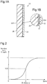
Fig. 1A is a cross-sectional view showing a decorative product. -
Fig. 1B is a partial enlarged cross-sectional view showing the decorative product. -
Fig. 2 is a graph showing the relationship of a depth from a surface (rear surface) of a transparent member and a secondary ionic strength of a fragment of an acrylic resin obtained through a TOF-SIMS analysis in the depth. - A decorative product according to one embodiment of the present invention will now be described.
- As shown in
Figs. 1A and 1B , adecorative product 10 includes atransparent member 20 including a first surface and a second surface, which is located at the opposite side of the first surface, and adecorative layer 30 sputtered onto the first surface of thetransparent member 20. In the following description, the first surface of thetransparent member 20 is referred to as therear surface 20r, and the second surface of thetransparent member 20 is referred to as thefront surface 20f. - The
transparent member 20 is a transparent or translucent member formed from an acrylic resin. When thedecorative product 10 is viewed from thetransparent member 20, thedecorative layer 30 is visually recognized. As long as thetransparent member 20 includes thefront surface 20f or therear surface 20r, the shape of thetransparent member 20 is not particularly limited and may be set in accordance with the application of thedecorative product 10. For example, at least one of thefront surface 20f and therear surface 20r of thetransparent member 20 may be curved or have irregularities. - A known acrylic resin such as a polymer including alkyl methacrylate, a polymer including alkyl acrylate, or a polymer including alkyl methacrylate and alkyl acrylate can be used as an acrylic resin that forms the
transparent member 20. Examples of the acrylic resin include polymethyl methacrylate (PMA) and polymethyl acrylate. Each of the polymers may be a copolymer that partially includes other monomers excluding alkyl methacrylate and alkyl acrylate. Examples of the other monomers include a compound including a vinyl group, a vinylene group, or a vinylidene group such as butene, isobutene, acrylamide, methacrylamide, styrene, acrylonitrile, and methacrylonitrile. Further, the degree of polymerization is not particularly limited and may range, for example, from 10000 to 15000. - As shown in
Fig. 1B , thetransparent member 20 includes a processedlayer 21 serving as a surface layer on therear surface 20r including thedecorative layer 30. The processedlayer 21 is a layered portion arranged to increase the adhesion between thetransparent member 20 and thedecorative layer 30. The processedlayer 21 is formed by performing a plasma treatment on thetransparent member 20. - In the plasma treatment, a source gas supplied to a vacuum is ionized by plasma, and ions of the source gas are irradiated on the
transparent member 20. The thickness L of the processedlayer 21 on the surface of thetransparent member 20 can be adjusted by adjusting the irradiation time of the ions in the plasma treatment and the power that accelerates the ions toward thetransparent member 20. Examples of the source gas used for the plasma treatment include inert gas such as argon and nitrogen, oxygen, hydrogen, and mixture gas of oxygen and hydrogen. A known method of a plasma treatment (for example, method disclosed in patent document 2) can be performed as the plasma treatment. - In particular, it is preferred that after performing the plasma treatment using inert gas as source gas, a treatment of exposing the
transparent member 20 to oxygen be performed as a treatment of forming the processedlayer 21 based on the plasma treatment. Examples of the treatment of exposing thetransparent member 20 to oxygen include performing a second plasma treatment using oxygen as source gas and leaving thetransparent member 20 under an oxygen atmosphere (for example, in air). This increases the adhesion, in particular, long-term adhesion, between thetransparent member 20 and thedecorative layer 30. - The result of analysis with Time-of-Flight Secondary Ion Mass Spectrometry (TOF-SIMS) indicates that the processed
layer 21 formed by performing a plasma treatment is a carbon layer formed when the molecular structure of the acrylic resin of thetransparent member 20 changes. That is, the analysis of the processedlayer 21 using TOF-SIMS allows for checking of the loss of the peak of C8H13O2 and C9H13O4 or the like, which is a fragment unique to an acrylic resin, and the formation of the peak of carbon, which is similar to diamond-like carbon. The result indicates that the processedlayer 21 is a layer formed when the molecular structure of the acrylic resin changes and is a layer of amorphous carbon having a structure of diamond-like carbon. - The thickness L of the processed layer M is less than or equal to 260 nm and is preferably less than or equal to 160 nm. Further, the lower limit value of the thickness L of the processed
layer 21 is not particularly limited and is preferably, for example, greater than or equal to 90 nm. When the processedlayer 21 is thick, the adhesion between thetransparent member 20 and thedecorative layer 30 tends to increase. - The thickness L of the processed layer M is defined as follows. The relationship of the depth from the
rear surface 20r of thetransparent member 20 and the secondary ionic strength of a fragment of an acrylic resin (for example, C8H13O2) obtained from the TOF-SIMS analysis in the depth is shown by the S-shaped curve inFig. 2 . In the curve ofFig. 2 , the secondary ionic strength is constant subsequent to a predetermined depth. In the curve, the depth (X) when the secondary ionic strength is one-half (Y/2) of the constant value (Y) of the secondary ionic strength subsequent to the predetermined depth is set to the thickness L of the processedlayer 21. When assuming that the portion of the processedlayer 21 of thetransparent member 20 is formed from an acrylic resin in the TOF-SIMS analysis, the value of the depth of thetransparent member 20 used for the graph ofFig. 2 is an acrylic resin converted value obtained based on an etching speed of an acrylic resin. - The
decorative layer 30 is a metal layer arranged on therear surface 20r of thetransparent member 20. Thedecorative layer 30 is formed on the processedlayer 21 of thetransparent member 20 by performing sputtering on which a plasma treatment is performed. The metal of thedecorative layer 30 includes known metal applicable to sputtering, for example, chrome, aluminum, indium, titanium, gold, silver, copper, and platinum. Further, the color tone of the metal layer is not particularly limited. - The
decorative product 10 of the present embodiment is applicable to various usages, for example, interior and exterior products for vehicles, interior and exterior components of a house or the like, and home appliances. Examples of the interior and exterior products for vehicles include an emblem and a back panel serving as a cover of a millimeter radar device. - The operation of the present embodiment will now be described.
- In a decorative product including a decorative layer on a transparent member formed from an acrylic resin by performing sputtering, the color tone of the decorative layer changes when a processed layer is arranged on the transparent member. This is because the decorative layer looks different when the decorative layer is viewed from the transparent member including the processed layer. That is, the formation of the processed layer decreases the transparency of light of the transparent member and changes the color of the transparent member. As a result, when the decorative layer is viewed through the transparent member, the color tone of the decorative layer looks different.
- The
decorative product 10 of the present embodiment includes the processedlayer 21. However, the thickness of the processedlayer 21 is less than or equal to 260 nm. This limits changes in the color tone of thedecorative layer 30 that would occur when thedecorative product 10 is viewed from thetransparent member 20. - The present embodiment has the advantages described below.
- (1) The
decorative product 10 includes thetransparent member 20 formed from an acrylic resin and thedecorative layer 30 arranged on therear surface 20r of thetransparent member 20. The processedlayer 21 formed by performing a plasma treatment on therear surface 20r (first surface) of thetransparent member 20 is arranged between thetransparent member 20 and thedecorative layer 30. Thedecorative layer 30 is a metal layer formed on the processedlayer 21 by performing sputtering. The thickness L of the processedlayer 21 is less than or equal to 260 nm. - In the structure, the
decorative layer 30 formed by performing sputtering is arranged on the processedlayer 21 of thetransparent member 20. This ensures the adhesion between thetransparent member 20 and thedecorative layer 30. Further, the processedlayer 21 has a thickness of less than or equal to 260 nm. This limits changes in the color tone of thedecorative layer 30 that would occur when thedecorative product 10 is viewed from thetransparent member 20. - (2) It is preferred that the thickness of the processed layer be greater than or equal to 90 nm.
- This further increases the adhesion between the
transparent member 20 and thedecorative layer 30. - (3) When the
decorative product 10 is manufactured, it is preferred that when a plasma treatment is performed to arrange the processedlayer 21 on thetransparent member 20, the second plasma treatment using oxygen be performed after the first plasma treatment using inert gas is performed. - This increases the adhesion, in particular, long-term adhesion, between the
transparent member 20 and thedecorative layer 30. - The present embodiment may be modified as described below.
- A second decorative layer may be arranged on the
front surface 20f (second surface) of thetransparent member 20. For example, when using a decorative layer that at least partially includes a transparent or translucent decorative portion, thedecorative layer 30 can be recognized through the decorative portion. Further, when the second decorative layer is arranged on only part of thefront surface 20f (second surface) of thetransparent member 20, thedecorative layer 30 can be recognized through the portion where the second decorative layer is not arranged. In these cases, when thedecorative layer 30 is viewed over the second decorative layer, thedecorative product 10 has a further complicated color tone and aesthetic appeal. - When the second decorative layer is arranged, the processed
layer 21 may also be arranged on thefront surface 20f (second surface) of thetransparent member 20. In this case, it is preferred that the total thickness of the two processedlayers 21 be less than or equal to 260 nm. - A protection layer, a protection member, or the like that protects the
decorative layer 30 may be arranged on the surface of thedecorative layer 30 located at the opposite side of thetransparent member 20. - Examples that further realize the embodiment will now be described.
- As shown in Table 1, decorative products of a reference example and experimental examples were manufactured under different treatment conditions of a plasma treatment performed on transparent members. Further, the changes in the color tone and the adhesion of the decorative layer in each example were evaluated.
- A transparent member (100 mm long × 100 mm wide × 3 mm thick) formed from PMMA was arranged at a predetermined position in a treatment chamber. The treatment chamber included two electrodes with the transparent member on the position located in between. The two electrodes were spaced apart from each other and located toward a front side and a rear side of the transparent member. After arranging the transparent member, the treatment chamber was set to a vacuum state, and the treatment chamber was supplied with a source gas converted into plasma. Then, voltage was applied to the two electrodes to generate a glow discharge, and a plasma treatment was performed on the surface (rear surface) of the transparent member. The plasma treatment was performed twice with different source gases. The first plasma treatment and the second plasma treatment were performed under the conditions described below. In the reference example, the first plasma treatment and the second plasma treatment were not performed. In experimental example 8, the second plasma treatment (treatment of exposing transparent member to oxygen) was not performed.
-
- Source gas: argon
- Gas flow rate: 50 sccm (0°C, 1 atm (1013 hPa)
- Power: 0.8 kW
- Treatment time: 10 to 70 seconds
- Second Treatment Condition
- Source gas: oxygen
- Gas flow rate: 30 sccm (0°C, 1 atm (1013 hPa)
- Power: 0.5 kW
- Treatment time: 10 seconds
- The thickness of the processed layer formed on each of the transparent members of experimental examples 1 to 4 and 8 subsequent to the plasma treatment was measured. The thickness of the processed layer was measured based on the secondary ionic strength of a fragment formed from an acrylic resin (C8H13O2) using a TOF-SIMS device (TOF. SIMS5, produced by ION-TOF). The measuring condition with the TOF-SIMS device is as follows.
-
- Measurement mode: high mass resolution
- Measurement surface: analysis in depth direction
- Measurement Area: 300 µm square
- Further, the thickness of each processed layer of the transparent member of experimental examples 5 to 7 subsequent to the plasma treatment was estimated from the thickness of each processed layer of the transparent member of experimental examples 1 to 4. More specifically, the thickness of each processed layer of experimental examples 5 to 7 was estimated from the treatment time of the plasma treatment of experimental examples 5 to 7 using an approximate line obtained by plotting on a graph the relationship of the thickness of each processed layer and the treatment time of the (first) plasma treatment in experimental examples 1
- The transparent member of each example subsequent to the plasma treatment was arranged at a predetermined position in the treatment chamber. The treatment chamber included two electrodes with the transparent member on the position located in between. The two electrodes were spaced apart from each other and located toward a front side and a rear side of the transparent member. Further, a sputtering target was arranged between the rear side of the transparent member and one of the electrodes. After arranging the transparent member, the treatment chamber was set to a vacuum state, and the treatment chamber was supplied with argon converted into plasma. Then, voltage was applied to the two electrodes to generate a glow discharge, and a decorative layer formed from a material of the sputtering target was formed on the surface (rear surface) of the transparent member. The decorative layer was formed under the following sputtering condition.
-
- Power: 0.5 kW
- Treatment time: 30 seconds
- <Evaluation>
- Evaluation of Color Tone
- The color tone (L*a*b* color system) of a side of the transparent member of the decorative product of each example was analyzed using a spectrophotometer (CM-700d, produced by Konica Minolta, Inc). Then, the b* value of the reference example less the processed layer and the b* value of each experimental example with the processed layer were compared to calculate a Δb* value, which is the degree of changes in the color tone, and the color tone of the decorative product of each experimental example was evaluated in the following three stages based on the Δb* value. The Δb* value can be calculated by subtracting the b* value of the reference example from the b* value of each experimental example. Table 1 shows the result.
- In Table 1, the symbols in the evaluation column □, ○, and × indicate the values described below and mean excellent, good, poor, respectively.
- □: Δb* value < 2
- ○: 2 ≤ Δb* value < 3
- x: 3 ≤ Δb* value
- Evaluation of Adhesion
- After forming the decorative layer, the decorative product of each example was left for 24 hours at an atmosphere temperature of 20°C (room temperature). Then, the adhesion of the decorative layer was measured by conducting a pull-off test in compliance with JIS K 5600-5-7 using a pull-off adhesion tester (positive test adhesion tester KH-AT-A, produced by COTEC, Ltd). Table 1 shows the result.
[Table 1] Reference Example Experimental Example1 Experimental Example2 Experimental Example3 Experimental Example 4 Experimental Example 5 Experimental Example6 Experimental Example 57 Experimental Example 8 First Treatment Time (Sec) 10 20 30 40 50 60 70 10 Thickness of Processed Layer (nm) 0 60 90 130 160 212 254 296 130 b* value 2.46 3.01 3.47 4.09 4.26 4.95 5.38 5.78 4.15 Δb* value - 0.55 1.01 1.63 1.8 2.49 2.92 3.32 1.69 Evaluation of Color Tone - □ □ □ □ ○ ○ × □ Separation Strength (Mpa) 0.28 0.94 1.06 1.13 1.3 1.53 1.96 2.05 0.65 - The result shown in Table 1 confirms the correlation of the thickness of the processed layer of the transparent member and the degree of changes in the color tone (Δb* value). When one of the thickness and the degree increases, the other one increases. The result shows that the arrangement of the processed layer in the transparent member changes the color tone of the decorative layer because the decorative layer looks different when the decorative layer is viewed through the transparent member including the processed layer, not because the color tone of the decorative layer changes (for example, the color of the decorative layer changes at a portion of the decorative layer contacting the processed layer).
- Thus, even when the processed layer is arranged on the transparent member, changes in the color tone of the decorative layer are limited by forming a thin processed layer. As shown in Table 1, even when a thin processed layer is formed, the effect of increasing the adhesion of the decorative layer (separation strength) by the processed layer is obtained.
- When the b* value increases, the color tone shifts toward yellow. Thus, as the processed layer thickens, the transparent member becomes yellow. This may result from the structure of diamond-like carbon forming the processed layer.
- The thickness of the processed layer is substantially the same in experimental example 3 and experimental example 8 in which the second plasma treatment using oxygen was not performed. However, experimental example 8 has a higher adhesion (separation strength) of the decorative layer than experimental example 3. The result confirms that the adhesion of the decorative layer can be increased by performing the second plasma treatment using oxygen, that is, the treatment of exposing the transparent member to oxygen.
-
- 10: Decorative product
- 20: Transparent member
- 21: Processed layer
- 30: Decorative layer
Claims (5)
- A decorative product comprising:a transparent member formed from an acrylic resin; anda decorative layer arranged on a first surface of the transparent member, wherein the decorative layer is visually recognized through the transparent member, whereina processed layer is located between the transparent member and the decorative layer, wherein the processed layer is formed by performing a plasma treatment on the first surface of the transparent member,the decorative layer is a metal layer formed on the processed layer by performing sputtering, andthe processed layer has a thickness of less than or equal to 260 nm.
- The decorative product according to claim 1, wherein the thickness of the processed layer is from 90 nm to 260 nm.
- The decorative product according to claim 1 or 2, wherein the processed layer is a layer having a structure of diamond-like carbon.
- A method for manufacturing the decorative product according to any one of claims 1 to 3, the method comprising the steps of:forming the processed layer on the first surface of the transparent member by performing a plasma treatment; andforming the decorative layer on the processed layer of the transparent member by performing sputtering after the step of forming the processed layer, whereinthe step of forming the processed layer includes performing a treatment for exposing the transparent member to oxygen after a plasma treatment using inert gas.
- A method for manufacturing a decorative product including a transparent member formed from an acrylic resin and a decorative layer arranged on a first surface of the transparent member, wherein the decorative layer is visually recognized through the transparent member, the method comprising the steps of:forming a processed layer on the first surface of the transparent member by performing a plasma treatment; andforming the decorative layer on the processed layer of the transparent member by performing sputtering after the step of forming the processed layer, whereinthe step of forming the processed layer includes performing a treatment for exposing the transparent member to oxygen after a plasma treatment using inert gas.
Applications Claiming Priority (2)
| Application Number | Priority Date | Filing Date | Title |
|---|---|---|---|
| JP2015071664A JP6344288B2 (en) | 2015-03-31 | 2015-03-31 | Decorative product and method for producing decorative product |
| PCT/JP2016/057789 WO2016158320A1 (en) | 2015-03-31 | 2016-03-11 | Decorative product and method of manufacturing decorative product |
Publications (3)
| Publication Number | Publication Date |
|---|---|
| EP3278979A1 true EP3278979A1 (en) | 2018-02-07 |
| EP3278979A4 EP3278979A4 (en) | 2018-12-05 |
| EP3278979B1 EP3278979B1 (en) | 2020-09-30 |
Family
ID=57005631
Family Applications (1)
| Application Number | Title | Priority Date | Filing Date |
|---|---|---|---|
| EP16772204.0A Active EP3278979B1 (en) | 2015-03-31 | 2016-03-11 | Decorative product and method of manufacturing decorative product |
Country Status (5)
| Country | Link |
|---|---|
| US (1) | US10259197B2 (en) |
| EP (1) | EP3278979B1 (en) |
| JP (1) | JP6344288B2 (en) |
| CN (1) | CN107428130B (en) |
| WO (1) | WO2016158320A1 (en) |
Families Citing this family (4)
| Publication number | Priority date | Publication date | Assignee | Title |
|---|---|---|---|---|
| CN109023232B (en) * | 2018-10-22 | 2020-12-01 | 中国科学院宁波材料技术与工程研究所 | A method for forming amorphous carbon film on the surface of plastic substrate |
| JP7610344B2 (en) | 2019-03-13 | 2025-01-08 | 三菱ケミカル株式会社 | (Meth)acrylic resin composition for millimeter wave radar cover, millimeter wave radar cover, millimeter wave radar device, and vehicle |
| JP7352238B2 (en) * | 2019-04-03 | 2023-09-28 | 上原ネームプレート工業株式会社 | Resin member and its manufacturing method |
| KR102829328B1 (en) * | 2019-12-16 | 2025-07-07 | 현대자동차주식회사 | Transmission cover of electromagnetic wave of radar for vehicle |
Family Cites Families (20)
| Publication number | Priority date | Publication date | Assignee | Title |
|---|---|---|---|---|
| US3686018A (en) * | 1970-11-02 | 1972-08-22 | Dow Chemical Co | Method of metallizing an organic substrate |
| JPH01263954A (en) | 1988-04-15 | 1989-10-20 | Hitachi Ltd | Optical system information recording medium and its manufacture |
| JPH0417660A (en) | 1990-05-11 | 1992-01-22 | Mitsubishi Rayon Co Ltd | Method of forming metal film on methacrylic resin |
| JPH04204502A (en) * | 1990-11-30 | 1992-07-24 | Toshiba Emi Ltd | Optical reflecting film and forming method therefor |
| JPH04325941A (en) | 1991-04-25 | 1992-11-16 | Sony Corp | Optical disk |
| JPH06289206A (en) | 1993-03-31 | 1994-10-18 | Toshiba Emi Ltd | Formation of optical reflecting film |
| US6083628A (en) * | 1994-11-04 | 2000-07-04 | Sigma Laboratories Of Arizona, Inc. | Hybrid polymer film |
| DE19844021C2 (en) | 1998-09-25 | 2001-05-10 | Daimler Chrysler Ag | Cladding part located within the beam path of a radar device |
| JP2000103883A (en) | 1998-09-30 | 2000-04-11 | Sony Corp | Surface modification process for plastics and information recording medium prepared by the process |
| JP2000103884A (en) | 1998-09-30 | 2000-04-11 | Sony Corp | Plastics surface modification method and plastics modified using the surface modification method |
| JP2001123263A (en) | 1999-10-27 | 2001-05-08 | Sumitomo Chem Co Ltd | Sputtering substrate and manufacturing method thereof |
| DE10304668B4 (en) * | 2003-02-05 | 2006-10-19 | König, Klaus-Peter | A method of adherent coating of a substrate comprising a metallic layer and its use |
| JP2005249773A (en) * | 2004-02-02 | 2005-09-15 | Toyota Motor Corp | Molded product for beam path of radar equipment |
| JP2006021377A (en) * | 2004-07-07 | 2006-01-26 | C I Kasei Co Ltd | Metallic film for decoration and manufacturing method thereof |
| JP2007227086A (en) * | 2006-02-22 | 2007-09-06 | Tokyo Electron Ltd | Film forming apparatus and light emitting element manufacturing method |
| JP4895897B2 (en) * | 2007-04-05 | 2012-03-14 | 株式会社シンクロン | Thin film structure and manufacturing method thereof |
| US20120301634A1 (en) * | 2010-01-27 | 2012-11-29 | Shuji Nakamura | Gas barrier film and process for producing the same, and device using the same |
| US20120251021A1 (en) * | 2011-04-04 | 2012-10-04 | Swei Gwo S | Self-lubricating structure and method of manufacturing same |
| JP5970914B2 (en) * | 2012-03-29 | 2016-08-17 | 大日本印刷株式会社 | Three-dimensional decorative film |
| ES2640919T3 (en) * | 2012-06-01 | 2017-11-07 | Covestro Deutschland Ag | Multilayer structure as reflector |
-
2015
- 2015-03-31 JP JP2015071664A patent/JP6344288B2/en active Active
-
2016
- 2016-03-11 CN CN201680013819.9A patent/CN107428130B/en active Active
- 2016-03-11 US US15/551,984 patent/US10259197B2/en active Active
- 2016-03-11 EP EP16772204.0A patent/EP3278979B1/en active Active
- 2016-03-11 WO PCT/JP2016/057789 patent/WO2016158320A1/en not_active Ceased
Also Published As
| Publication number | Publication date |
|---|---|
| US20180029333A1 (en) | 2018-02-01 |
| JP6344288B2 (en) | 2018-06-20 |
| US10259197B2 (en) | 2019-04-16 |
| WO2016158320A1 (en) | 2016-10-06 |
| CN107428130A (en) | 2017-12-01 |
| CN107428130B (en) | 2019-11-12 |
| EP3278979B1 (en) | 2020-09-30 |
| EP3278979A4 (en) | 2018-12-05 |
| JP2016190401A (en) | 2016-11-10 |
Similar Documents
| Publication | Publication Date | Title |
|---|---|---|
| EP3278979B1 (en) | Decorative product and method of manufacturing decorative product | |
| US8894827B2 (en) | Electrochromic tungsten oxide film deposition | |
| EP3018505A1 (en) | Radio wave penetration-type multilayer optical coating | |
| Kolfschoten et al. | Argon‐ion assisted etching of silicon by molecular chlorine | |
| JPWO2011048647A1 (en) | Transparent conductive film and touch panel using the same | |
| US20070224412A1 (en) | Transparent Conductive Laminated Body and Transparent Touch-Sensitive Panel | |
| Ninomiya et al. | A fragment-free ionization technique for organic mass spectrometry with large Ar cluster ions | |
| JP5412850B2 (en) | Gas barrier laminate | |
| EP1310982A3 (en) | Time-of-flight mass spectrometer | |
| US20130105299A1 (en) | Vacuum deposition method for forming gradient patterns using vacuum device | |
| JP2009283348A (en) | Transparent conductive film, and touch panel using the same | |
| Welzel et al. | Ion energy distributions in magnetron sputtering of zinc aluminium oxide | |
| US20080278457A1 (en) | Acrylic resin, resin boards, transparent electrode boards for touch panels, touch panels, and processes for production of them | |
| JP4135079B2 (en) | Transparent conductive film, method for producing transparent conductive sheet, and touch panel | |
| Thomson et al. | Electron emission properties of insulator materials pertinent to the International Space Station | |
| US20140072721A1 (en) | Method for Modifying a Surface of a Substrate using Ion Bombardment | |
| JP5834894B2 (en) | Method for producing transparent conductive film | |
| JP5196001B2 (en) | Transparent conductive film and method for producing the same | |
| KR101028514B1 (en) | Manufacturing method of sunscreen film | |
| Samartsev et al. | Yields and ionization probabilities of sputtered Inn particles under atomic and polyatomic Aum− ion bombardment | |
| WO2007013220A1 (en) | Transparent electrically conductive film, transparent electrically conductive sheet, and touch panel | |
| Lee et al. | Linear ion beam applications for roll-to-roll metal thin film coatings on PET substrates | |
| Zeuner et al. | Characterisation of DC unbalanced magnetron deposition of Ni⧹ C: H composite films | |
| JP7581727B2 (en) | Gas barrier film manufacturing method and gas barrier film | |
| US20250294715A1 (en) | Method for producing transparent conductive coatings for emi protection using hipims |
Legal Events
| Date | Code | Title | Description |
|---|---|---|---|
| STAA | Information on the status of an ep patent application or granted ep patent |
Free format text: STATUS: THE INTERNATIONAL PUBLICATION HAS BEEN MADE |
|
| PUAI | Public reference made under article 153(3) epc to a published international application that has entered the european phase |
Free format text: ORIGINAL CODE: 0009012 |
|
| STAA | Information on the status of an ep patent application or granted ep patent |
Free format text: STATUS: REQUEST FOR EXAMINATION WAS MADE |
|
| 17P | Request for examination filed |
Effective date: 20170821 |
|
| AK | Designated contracting states |
Kind code of ref document: A1 Designated state(s): AL AT BE BG CH CY CZ DE DK EE ES FI FR GB GR HR HU IE IS IT LI LT LU LV MC MK MT NL NO PL PT RO RS SE SI SK SM TR |
|
| AX | Request for extension of the european patent |
Extension state: BA ME |
|
| DAV | Request for validation of the european patent (deleted) | ||
| DAX | Request for extension of the european patent (deleted) | ||
| A4 | Supplementary search report drawn up and despatched |
Effective date: 20181029 |
|
| RIC1 | Information provided on ipc code assigned before grant |
Ipc: C23C 14/00 20060101ALI20181023BHEP Ipc: B32B 15/082 20060101AFI20181023BHEP Ipc: C23C 14/02 20060101ALI20181023BHEP Ipc: B32B 27/30 20060101ALI20181023BHEP Ipc: C23C 14/20 20060101ALI20181023BHEP Ipc: C23C 14/06 20060101ALI20181023BHEP |
|
| STAA | Information on the status of an ep patent application or granted ep patent |
Free format text: STATUS: EXAMINATION IS IN PROGRESS |
|
| 17Q | First examination report despatched |
Effective date: 20190705 |
|
| GRAP | Despatch of communication of intention to grant a patent |
Free format text: ORIGINAL CODE: EPIDOSNIGR1 |
|
| STAA | Information on the status of an ep patent application or granted ep patent |
Free format text: STATUS: GRANT OF PATENT IS INTENDED |
|
| INTG | Intention to grant announced |
Effective date: 20200525 |
|
| GRAS | Grant fee paid |
Free format text: ORIGINAL CODE: EPIDOSNIGR3 |
|
| GRAA | (expected) grant |
Free format text: ORIGINAL CODE: 0009210 |
|
| STAA | Information on the status of an ep patent application or granted ep patent |
Free format text: STATUS: THE PATENT HAS BEEN GRANTED |
|
| AK | Designated contracting states |
Kind code of ref document: B1 Designated state(s): AL AT BE BG CH CY CZ DE DK EE ES FI FR GB GR HR HU IE IS IT LI LT LU LV MC MK MT NL NO PL PT RO RS SE SI SK SM TR |
|
| REG | Reference to a national code |
Ref country code: CH Ref legal event code: EP Ref country code: GB Ref legal event code: FG4D |
|
| REG | Reference to a national code |
Ref country code: AT Ref legal event code: REF Ref document number: 1318387 Country of ref document: AT Kind code of ref document: T Effective date: 20201015 |
|
| REG | Reference to a national code |
Ref country code: DE Ref legal event code: R096 Ref document number: 602016045027 Country of ref document: DE |
|
| REG | Reference to a national code |
Ref country code: IE Ref legal event code: FG4D |
|
| PG25 | Lapsed in a contracting state [announced via postgrant information from national office to epo] |
Ref country code: HR Free format text: LAPSE BECAUSE OF FAILURE TO SUBMIT A TRANSLATION OF THE DESCRIPTION OR TO PAY THE FEE WITHIN THE PRESCRIBED TIME-LIMIT Effective date: 20200930 Ref country code: BG Free format text: LAPSE BECAUSE OF FAILURE TO SUBMIT A TRANSLATION OF THE DESCRIPTION OR TO PAY THE FEE WITHIN THE PRESCRIBED TIME-LIMIT Effective date: 20201230 Ref country code: NO Free format text: LAPSE BECAUSE OF FAILURE TO SUBMIT A TRANSLATION OF THE DESCRIPTION OR TO PAY THE FEE WITHIN THE PRESCRIBED TIME-LIMIT Effective date: 20201230 Ref country code: SE Free format text: LAPSE BECAUSE OF FAILURE TO SUBMIT A TRANSLATION OF THE DESCRIPTION OR TO PAY THE FEE WITHIN THE PRESCRIBED TIME-LIMIT Effective date: 20200930 Ref country code: GR Free format text: LAPSE BECAUSE OF FAILURE TO SUBMIT A TRANSLATION OF THE DESCRIPTION OR TO PAY THE FEE WITHIN THE PRESCRIBED TIME-LIMIT Effective date: 20201231 Ref country code: FI Free format text: LAPSE BECAUSE OF FAILURE TO SUBMIT A TRANSLATION OF THE DESCRIPTION OR TO PAY THE FEE WITHIN THE PRESCRIBED TIME-LIMIT Effective date: 20200930 |
|
| REG | Reference to a national code |
Ref country code: AT Ref legal event code: MK05 Ref document number: 1318387 Country of ref document: AT Kind code of ref document: T Effective date: 20200930 |
|
| PG25 | Lapsed in a contracting state [announced via postgrant information from national office to epo] |
Ref country code: RS Free format text: LAPSE BECAUSE OF FAILURE TO SUBMIT A TRANSLATION OF THE DESCRIPTION OR TO PAY THE FEE WITHIN THE PRESCRIBED TIME-LIMIT Effective date: 20200930 Ref country code: LV Free format text: LAPSE BECAUSE OF FAILURE TO SUBMIT A TRANSLATION OF THE DESCRIPTION OR TO PAY THE FEE WITHIN THE PRESCRIBED TIME-LIMIT Effective date: 20200930 |
|
| REG | Reference to a national code |
Ref country code: NL Ref legal event code: MP Effective date: 20200930 |
|
| REG | Reference to a national code |
Ref country code: LT Ref legal event code: MG4D |
|
| PG25 | Lapsed in a contracting state [announced via postgrant information from national office to epo] |
Ref country code: SM Free format text: LAPSE BECAUSE OF FAILURE TO SUBMIT A TRANSLATION OF THE DESCRIPTION OR TO PAY THE FEE WITHIN THE PRESCRIBED TIME-LIMIT Effective date: 20200930 Ref country code: EE Free format text: LAPSE BECAUSE OF FAILURE TO SUBMIT A TRANSLATION OF THE DESCRIPTION OR TO PAY THE FEE WITHIN THE PRESCRIBED TIME-LIMIT Effective date: 20200930 Ref country code: LT Free format text: LAPSE BECAUSE OF FAILURE TO SUBMIT A TRANSLATION OF THE DESCRIPTION OR TO PAY THE FEE WITHIN THE PRESCRIBED TIME-LIMIT Effective date: 20200930 Ref country code: NL Free format text: LAPSE BECAUSE OF FAILURE TO SUBMIT A TRANSLATION OF THE DESCRIPTION OR TO PAY THE FEE WITHIN THE PRESCRIBED TIME-LIMIT Effective date: 20200930 Ref country code: RO Free format text: LAPSE BECAUSE OF FAILURE TO SUBMIT A TRANSLATION OF THE DESCRIPTION OR TO PAY THE FEE WITHIN THE PRESCRIBED TIME-LIMIT Effective date: 20200930 Ref country code: PT Free format text: LAPSE BECAUSE OF FAILURE TO SUBMIT A TRANSLATION OF THE DESCRIPTION OR TO PAY THE FEE WITHIN THE PRESCRIBED TIME-LIMIT Effective date: 20210201 Ref country code: CZ Free format text: LAPSE BECAUSE OF FAILURE TO SUBMIT A TRANSLATION OF THE DESCRIPTION OR TO PAY THE FEE WITHIN THE PRESCRIBED TIME-LIMIT Effective date: 20200930 |
|
| PG25 | Lapsed in a contracting state [announced via postgrant information from national office to epo] |
Ref country code: PL Free format text: LAPSE BECAUSE OF FAILURE TO SUBMIT A TRANSLATION OF THE DESCRIPTION OR TO PAY THE FEE WITHIN THE PRESCRIBED TIME-LIMIT Effective date: 20200930 Ref country code: IS Free format text: LAPSE BECAUSE OF FAILURE TO SUBMIT A TRANSLATION OF THE DESCRIPTION OR TO PAY THE FEE WITHIN THE PRESCRIBED TIME-LIMIT Effective date: 20210130 Ref country code: AT Free format text: LAPSE BECAUSE OF FAILURE TO SUBMIT A TRANSLATION OF THE DESCRIPTION OR TO PAY THE FEE WITHIN THE PRESCRIBED TIME-LIMIT Effective date: 20200930 Ref country code: AL Free format text: LAPSE BECAUSE OF FAILURE TO SUBMIT A TRANSLATION OF THE DESCRIPTION OR TO PAY THE FEE WITHIN THE PRESCRIBED TIME-LIMIT Effective date: 20200930 Ref country code: ES Free format text: LAPSE BECAUSE OF FAILURE TO SUBMIT A TRANSLATION OF THE DESCRIPTION OR TO PAY THE FEE WITHIN THE PRESCRIBED TIME-LIMIT Effective date: 20200930 |
|
| PG25 | Lapsed in a contracting state [announced via postgrant information from national office to epo] |
Ref country code: SK Free format text: LAPSE BECAUSE OF FAILURE TO SUBMIT A TRANSLATION OF THE DESCRIPTION OR TO PAY THE FEE WITHIN THE PRESCRIBED TIME-LIMIT Effective date: 20200930 |
|
| REG | Reference to a national code |
Ref country code: DE Ref legal event code: R097 Ref document number: 602016045027 Country of ref document: DE |
|
| PLBE | No opposition filed within time limit |
Free format text: ORIGINAL CODE: 0009261 |
|
| STAA | Information on the status of an ep patent application or granted ep patent |
Free format text: STATUS: NO OPPOSITION FILED WITHIN TIME LIMIT |
|
| PG25 | Lapsed in a contracting state [announced via postgrant information from national office to epo] |
Ref country code: DK Free format text: LAPSE BECAUSE OF FAILURE TO SUBMIT A TRANSLATION OF THE DESCRIPTION OR TO PAY THE FEE WITHIN THE PRESCRIBED TIME-LIMIT Effective date: 20200930 |
|
| 26N | No opposition filed |
Effective date: 20210701 |
|
| PG25 | Lapsed in a contracting state [announced via postgrant information from national office to epo] |
Ref country code: IT Free format text: LAPSE BECAUSE OF FAILURE TO SUBMIT A TRANSLATION OF THE DESCRIPTION OR TO PAY THE FEE WITHIN THE PRESCRIBED TIME-LIMIT Effective date: 20200930 Ref country code: MC Free format text: LAPSE BECAUSE OF FAILURE TO SUBMIT A TRANSLATION OF THE DESCRIPTION OR TO PAY THE FEE WITHIN THE PRESCRIBED TIME-LIMIT Effective date: 20200930 |
|
| REG | Reference to a national code |
Ref country code: CH Ref legal event code: PL |
|
| GBPC | Gb: european patent ceased through non-payment of renewal fee |
Effective date: 20210311 |
|
| PG25 | Lapsed in a contracting state [announced via postgrant information from national office to epo] |
Ref country code: SI Free format text: LAPSE BECAUSE OF FAILURE TO SUBMIT A TRANSLATION OF THE DESCRIPTION OR TO PAY THE FEE WITHIN THE PRESCRIBED TIME-LIMIT Effective date: 20200930 |
|
| REG | Reference to a national code |
Ref country code: BE Ref legal event code: MM Effective date: 20210331 |
|
| PG25 | Lapsed in a contracting state [announced via postgrant information from national office to epo] |
Ref country code: CH Free format text: LAPSE BECAUSE OF NON-PAYMENT OF DUE FEES Effective date: 20210331 Ref country code: LI Free format text: LAPSE BECAUSE OF NON-PAYMENT OF DUE FEES Effective date: 20210331 Ref country code: LU Free format text: LAPSE BECAUSE OF NON-PAYMENT OF DUE FEES Effective date: 20210311 Ref country code: IE Free format text: LAPSE BECAUSE OF NON-PAYMENT OF DUE FEES Effective date: 20210311 Ref country code: FR Free format text: LAPSE BECAUSE OF NON-PAYMENT OF DUE FEES Effective date: 20210331 Ref country code: GB Free format text: LAPSE BECAUSE OF NON-PAYMENT OF DUE FEES Effective date: 20210311 |
|
| PG25 | Lapsed in a contracting state [announced via postgrant information from national office to epo] |
Ref country code: IS Free format text: LAPSE BECAUSE OF FAILURE TO SUBMIT A TRANSLATION OF THE DESCRIPTION OR TO PAY THE FEE WITHIN THE PRESCRIBED TIME-LIMIT Effective date: 20210130 |
|
| PG25 | Lapsed in a contracting state [announced via postgrant information from national office to epo] |
Ref country code: BE Free format text: LAPSE BECAUSE OF NON-PAYMENT OF DUE FEES Effective date: 20210331 |
|
| PG25 | Lapsed in a contracting state [announced via postgrant information from national office to epo] |
Ref country code: CY Free format text: LAPSE BECAUSE OF FAILURE TO SUBMIT A TRANSLATION OF THE DESCRIPTION OR TO PAY THE FEE WITHIN THE PRESCRIBED TIME-LIMIT Effective date: 20200930 |
|
| PG25 | Lapsed in a contracting state [announced via postgrant information from national office to epo] |
Ref country code: HU Free format text: LAPSE BECAUSE OF FAILURE TO SUBMIT A TRANSLATION OF THE DESCRIPTION OR TO PAY THE FEE WITHIN THE PRESCRIBED TIME-LIMIT; INVALID AB INITIO Effective date: 20160311 |
|
| PG25 | Lapsed in a contracting state [announced via postgrant information from national office to epo] |
Ref country code: MK Free format text: LAPSE BECAUSE OF FAILURE TO SUBMIT A TRANSLATION OF THE DESCRIPTION OR TO PAY THE FEE WITHIN THE PRESCRIBED TIME-LIMIT Effective date: 20200930 |
|
| PG25 | Lapsed in a contracting state [announced via postgrant information from national office to epo] |
Ref country code: MT Free format text: LAPSE BECAUSE OF FAILURE TO SUBMIT A TRANSLATION OF THE DESCRIPTION OR TO PAY THE FEE WITHIN THE PRESCRIBED TIME-LIMIT Effective date: 20200930 |
|
| PG25 | Lapsed in a contracting state [announced via postgrant information from national office to epo] |
Ref country code: TR Free format text: LAPSE BECAUSE OF FAILURE TO SUBMIT A TRANSLATION OF THE DESCRIPTION OR TO PAY THE FEE WITHIN THE PRESCRIBED TIME-LIMIT Effective date: 20200930 |
|
| PGFP | Annual fee paid to national office [announced via postgrant information from national office to epo] |
Ref country code: DE Payment date: 20260128 Year of fee payment: 11 |