EP3278182B1 - Electrophotographic printing - Google Patents
Electrophotographic printing Download PDFInfo
- Publication number
- EP3278182B1 EP3278182B1 EP15745194.9A EP15745194A EP3278182B1 EP 3278182 B1 EP3278182 B1 EP 3278182B1 EP 15745194 A EP15745194 A EP 15745194A EP 3278182 B1 EP3278182 B1 EP 3278182B1
- Authority
- EP
- European Patent Office
- Prior art keywords
- photoconductive
- photoconductive drum
- edge
- drum
- cleaning
- Prior art date
- Legal status (The legal status is an assumption and is not a legal conclusion. Google has not performed a legal analysis and makes no representation as to the accuracy of the status listed.)
- Active
Links
Images
Classifications
-
- G—PHYSICS
- G03—PHOTOGRAPHY; CINEMATOGRAPHY; ANALOGOUS TECHNIQUES USING WAVES OTHER THAN OPTICAL WAVES; ELECTROGRAPHY; HOLOGRAPHY
- G03G—ELECTROGRAPHY; ELECTROPHOTOGRAPHY; MAGNETOGRAPHY
- G03G21/00—Arrangements not provided for by groups G03G13/00 - G03G19/00, e.g. cleaning, elimination of residual charge
- G03G21/0005—Arrangements not provided for by groups G03G13/00 - G03G19/00, e.g. cleaning, elimination of residual charge for removing solid developer or debris from the electrographic recording medium
- G03G21/0011—Arrangements not provided for by groups G03G13/00 - G03G19/00, e.g. cleaning, elimination of residual charge for removing solid developer or debris from the electrographic recording medium using a blade; Details of cleaning blades, e.g. blade shape, layer forming
- G03G21/0017—Details relating to the internal structure or chemical composition of the blades
-
- G—PHYSICS
- G03—PHOTOGRAPHY; CINEMATOGRAPHY; ANALOGOUS TECHNIQUES USING WAVES OTHER THAN OPTICAL WAVES; ELECTROGRAPHY; HOLOGRAPHY
- G03G—ELECTROGRAPHY; ELECTROPHOTOGRAPHY; MAGNETOGRAPHY
- G03G21/00—Arrangements not provided for by groups G03G13/00 - G03G19/00, e.g. cleaning, elimination of residual charge
- G03G21/0005—Arrangements not provided for by groups G03G13/00 - G03G19/00, e.g. cleaning, elimination of residual charge for removing solid developer or debris from the electrographic recording medium
- G03G21/0011—Arrangements not provided for by groups G03G13/00 - G03G19/00, e.g. cleaning, elimination of residual charge for removing solid developer or debris from the electrographic recording medium using a blade; Details of cleaning blades, e.g. blade shape, layer forming
-
- G—PHYSICS
- G03—PHOTOGRAPHY; CINEMATOGRAPHY; ANALOGOUS TECHNIQUES USING WAVES OTHER THAN OPTICAL WAVES; ELECTROGRAPHY; HOLOGRAPHY
- G03G—ELECTROGRAPHY; ELECTROPHOTOGRAPHY; MAGNETOGRAPHY
- G03G21/00—Arrangements not provided for by groups G03G13/00 - G03G19/00, e.g. cleaning, elimination of residual charge
- G03G21/0005—Arrangements not provided for by groups G03G13/00 - G03G19/00, e.g. cleaning, elimination of residual charge for removing solid developer or debris from the electrographic recording medium
- G03G21/007—Arrangement or disposition of parts of the cleaning unit
- G03G21/0076—Plural or sequential cleaning devices
-
- G—PHYSICS
- G03—PHOTOGRAPHY; CINEMATOGRAPHY; ANALOGOUS TECHNIQUES USING WAVES OTHER THAN OPTICAL WAVES; ELECTROGRAPHY; HOLOGRAPHY
- G03G—ELECTROGRAPHY; ELECTROPHOTOGRAPHY; MAGNETOGRAPHY
- G03G21/00—Arrangements not provided for by groups G03G13/00 - G03G19/00, e.g. cleaning, elimination of residual charge
- G03G21/0088—Arrangements not provided for by groups G03G13/00 - G03G19/00, e.g. cleaning, elimination of residual charge removing liquid developer
-
- G—PHYSICS
- G03—PHOTOGRAPHY; CINEMATOGRAPHY; ANALOGOUS TECHNIQUES USING WAVES OTHER THAN OPTICAL WAVES; ELECTROGRAPHY; HOLOGRAPHY
- G03G—ELECTROGRAPHY; ELECTROPHOTOGRAPHY; MAGNETOGRAPHY
- G03G21/00—Arrangements not provided for by groups G03G13/00 - G03G19/00, e.g. cleaning, elimination of residual charge
- G03G21/0094—Arrangements not provided for by groups G03G13/00 - G03G19/00, e.g. cleaning, elimination of residual charge fatigue treatment of the photoconductor
-
- G—PHYSICS
- G03—PHOTOGRAPHY; CINEMATOGRAPHY; ANALOGOUS TECHNIQUES USING WAVES OTHER THAN OPTICAL WAVES; ELECTROGRAPHY; HOLOGRAPHY
- G03G—ELECTROGRAPHY; ELECTROPHOTOGRAPHY; MAGNETOGRAPHY
- G03G2221/00—Processes not provided for by group G03G2215/00, e.g. cleaning or residual charge elimination
- G03G2221/0005—Cleaning of residual toner
- G03G2221/001—Plural sequential cleaning devices
-
- G—PHYSICS
- G03—PHOTOGRAPHY; CINEMATOGRAPHY; ANALOGOUS TECHNIQUES USING WAVES OTHER THAN OPTICAL WAVES; ELECTROGRAPHY; HOLOGRAPHY
- G03G—ELECTROGRAPHY; ELECTROPHOTOGRAPHY; MAGNETOGRAPHY
- G03G2221/00—Processes not provided for by group G03G2215/00, e.g. cleaning or residual charge elimination
- G03G2221/0026—Cleaning of foreign matter, e.g. paper powder, from imaging member
- G03G2221/0068—Cleaning mechanism
- G03G2221/0084—Liquid
Definitions
- Electrophotographic printing devices such as laser printing devices, form images on media like paper.
- a photoconductive drum is charged over its entire surface, and then selectively discharged in accordance with the image to be formed.
- Charged colorant such as dry or liquid ink or toner adheres to locations on the drum that have been discharged, and the colorant is then directly or indirectly transferred from the drum to the media.
- the photoconductive drum is discharged and remaining colorant on the drum is removed before repeating the image-formation process.
- JP H04 287081 A discloses an image forming device and a cleaning means to clean the surface of a photosensitive body of the image forming device.
- JP 2001 154553 A discloses a cleaning blade for cleaning a photosensitive drum, the cleaning blade comprising a planar cured body.
- JP 2002 132106 A discloses an image forming device with a liquid developing device and a cleaning device, the cleaning device to apply a cleaning liquid to the surface of a photoreceptor.
- US 2012/0275836 A1 describes a method of maintaining a photoconductive member of an image forming apparatus.
- Photoconductive drums can be fabricated from a variety of different materials. Some materials have relatively short lifespans; for example, organic photoconductive foil drums may have a lifetime of about 100,000 image-forming impressions. Other materials can have much longer lifespans; for example, amorphous silicon photoconductive drums may have a lifetime greater than 1,000,000 image-forming impressions.
- a drawback to using photoconductive drums having greater longevity is that their ability to form images on media without impairing image-formation quality is degraded. Specifically, dirt, debris, and other contaminants may over time stick to the drum. As the photoconductive drum ages, a sufficient amount of such contaminants stick to the drum to visibly affect image-formation quality. That is, undesired artifacts such as dark specks and marks may be visually evident on the media on which images are formed, and/or blank spots where colorant should have been deposited but has not been may become visually evident on such media.
- the photoconductive drum is discharged and remaining colorant removed before the image-formation process is repeated. Removal of the colorant is achieved by rotating the drum against a sponge impregnated with a cleaning solution or fluid. The photoconductive drum is then rotated against a wiper to remove the cleaning solution from the drum before the image-formation process is repeated.
- designers of electrophotographic printing devices have sought to maximize the extent to which the cleaning solution is removed by the wiper. In actuality a small amount of cleaning solution typically remains after wiping, on the order of tens of nanometers in thickness, although this has not been seen as desirable.
- Purposefully maintaining a relatively thick layer of cleaning solution on the photoconductive drum is to great degree illogical, insofar as the inclusion of a wiper within an electrophotographic printing device is conventionally meant to remove the solution from the drum to the greatest degree possible.
- the inventors have discovered, for instance, that purposefully rounding the edge of the wiper that comes into contact with the photoconductive drum maintains a layer of cleaning solution on the drum greater than one-hundred nanometers in thickness during wiping.
- the wiper has at least a nominally sharp edge to maximize cleaning solution removal from the drum, such that the amount that remains after wiping is on the order of tens of nanometers in thickness.
- the thickness of the cleaning solution layer maintained on photoconductive drum during wiping is generally great enough to promote longevity of the drum's ability to form images on media without image quality degradation, but not great enough to interfere with charging of the drum at the beginning of the image-formation process. That is, too thick of a layer of cleaning solution remaining on the photoconductive drum can result in an insulating layer that prevents the charger roller, corona wire, or other charging mechanism from uniformly charging the surface of the drum before being selectively discharged in correspondence with the image to be formed on the media. This is another reason why typically wipers have had nominally sharp edges to maximize removal of the cleaning solution from the photoconductive drum.
- a relatively thick cleaning solution layer can protect the surface of the photoconductive drum itself from becoming damaged by contaminants like dirt and debris. The contaminants are less likely to become lodged into the drum's surface when a relatively thick layer of cleaning solution coats the photoconductive drum, and such contaminants are more likely to be removed the next time the drum rotates past the sponge or wiper.
- a relatively thick cleaning solution layer on the photoconductive drum can protect the drum when it is being charged; the charging process subjects the photoconductive drum to harsh conditions in which ozone can be present and in which the drum is bombarded with electrons.
- a rotating transfer roller 112 in one implementation transfers the colorant from the drum 102 onto the media 116 that is advancing from left to right between the transfer roller 112 and a rotating impression roller 114. In another implementation, the drum 102 transfers the colorant directly onto the media 116.
- the photoconductive drum 102 rotates past a cleaning assembly 120 to completely discharge its photoconductive surface and remove any colorant still thereon before repeating the described process via being charged by the charge roller 104.
- the sponge 202 is impregnated with a cleaning solution or fluid, such as isoparaffinic fluid, and can be in physical contact with the photoconductive drum 102.
- the sponge 202 may, for instance, by in fluidic contact with a supply of the cleaning solution that replenishes the sponge 202 and keeps the sponge 202 continuously moist with the solution.
- the photoconductive drum 102 rotates past the sponge 202, the physical interaction between the sponge 202 and the drum 102, and/or the physical and/or chemical interaction between the cleaning fluid and the drum 102, cleans or removes any colorant 206 remaining on the drum 102.
- a thick layer 208 of the cleaning solution remains on the drum 102.
- a layer 210 of the cleaning solution remains on the photoconductive drum 102 after the drum 102 has rotated past the wiper 204.
- the thickness of the layer 210 of the cleaning solution that remains on the drum 102 after rotating past the wiper 204 is less than the thickness of the layer 208 that remains before rotating past the wiper 204.
- the thickness of the cleaning solution layer 210 is still relatively thick, and is greater than the thickness of a layer of cleaning solution that would otherwise remain if maximal removal of the cleaning solution by the wiper 204 were desired.
- FIGs. 3 and 4 show an example wiper 204 of the cleaning assembly 120 of the electrophotographic printing device 100.
- the edge 212 of the wiper 204 that is closest to the photoconductive drum 102 in FIG. 2 is purposefully rounded, curved, or non-nominally sharp. Purposefully rounding the edge 212 increases the thickness of the cleaning solution layer 210 that remains after the photoconductive drum 102 rotates past the wiper 204. As depicted in FIGs. 3 and 4 , the rounded edge 212 can be semi-circular.
- the cleaning solution layer 210 that remains on the photoconductive drum 102 after rotating past the wiper 204 in FIG. 2 can be about 300 nanometers in thickness.
- the edge 102 may have a radius between 1.5 millimeters and 10.0 millimeters, or even more generally, between 0.1 millimeters and 100 millimeters. A radius within this range may maintain a sufficiently thick cleaning solution 210 on the photoconductive drum 102 during wiping by the wiper 204 to promote longevity of the drum 102's ability to form images without impairing quality and longevity of the drum 102 itself while not being so great as to interfere with charging of the drum 102 by the charge roller 104 of FIG. 1 .
- edges 302, 304, and 306 of the wiper 204 can remain nominally sharp because they are not in contact with the photoconductive drum 102.
- the edges 302, 304, and 306 of the wiper 204 are also rounded, curved, or non-nominally sharp, like the edge 212. This is because the wiper 204 may be removably positionable in relation to the photoconductive drum 102. When the edge 212 wears out over time, for instance, the wiper 204 may be repositioned so that another edge 302, 304, or 306 becomes closest to the photoconductive drum 102.
- FIG. 5 shows an example method 500 that the electrophotographic printing device 100 performs.
- the photoconductive drum 102 of the printing device 100 is rotated (502). As the photoconductive drum 102 rotates, the following occurs. Colorant is transferred onto the media 116 from the photoconductive drum 102 (504). That is, the photoconductive drum 102's surface is charged by the charge roller 104, and selectively discharged by the discharge mechanism 106 in accordance with the image to be formed on the media 116. Colorant applied to the photoconductive drum 102 by the dispensing roller 108 in accordance with the image, and then transferred from the drum 102 to the media 116 via the transfer roller 112. Remaining colorant on the photoconductive drum 102 is removed by the sponge 202 using the cleaning solution (506), and the cleaning solution is wiped from the drum 102 by the wiper 204 as described (508), before the process is repeated at part 504 for another image.
Landscapes
- Physics & Mathematics (AREA)
- General Physics & Mathematics (AREA)
- Cleaning In Electrography (AREA)
- Discharging, Photosensitive Material Shape In Electrophotography (AREA)
Description
- Electrophotographic printing devices, such as laser printing devices, form images on media like paper. In general, a photoconductive drum is charged over its entire surface, and then selectively discharged in accordance with the image to be formed. Charged colorant such as dry or liquid ink or toner adheres to locations on the drum that have been discharged, and the colorant is then directly or indirectly transferred from the drum to the media. The photoconductive drum is discharged and remaining colorant on the drum is removed before repeating the image-formation process.
-
JP H04 287081 A JP 2001 154553 A JP 2002 132106 A US 2012/0275836 A1 describes a method of maintaining a photoconductive member of an image forming apparatus. - The scope of the invention is defined by the appended claims. Further embodiments of the invention are defined by the dependent claims. The embodiments which do not fall within the scope of the appended set of claims are to be interpreted as example embodiments of background information, useful only for understanding the invention.
-
-
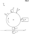
FIG. 1 is a diagram of an example electrophotographic printing device. -
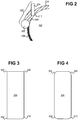
FIG. 2 is a diagram of an example cleaning assembly of an electrophotographic printing device. -
FIG. 3 is a diagram of an example wiper of a cleaning assembly of an electrophotographic printing device to assist cleaning of the photoconductive drum of the device. -
FIG. 4 is a diagram of another example wiper of a cleaning assembly of an electrophotographic printing device to assist cleaning of the photoconductive drum of the device. -
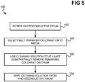
FIG. 5 is a flowchart of an example method performed by an electrophotographic printing device. - As noted in the background section, in an electrophotographic printing device, a photoconductive drum is used to transfer colorant onto media to form images on the media. Photoconductive drums can be fabricated from a variety of different materials. Some materials have relatively short lifespans; for example, organic photoconductive foil drums may have a lifetime of about 100,000 image-forming impressions. Other materials can have much longer lifespans; for example, amorphous silicon photoconductive drums may have a lifetime greater than 1,000,000 image-forming impressions.
- A drawback to using photoconductive drums having greater longevity is that their ability to form images on media without impairing image-formation quality is degraded. Specifically, dirt, debris, and other contaminants may over time stick to the drum. As the photoconductive drum ages, a sufficient amount of such contaminants stick to the drum to visibly affect image-formation quality. That is, undesired artifacts such as dark specks and marks may be visually evident on the media on which images are formed, and/or blank spots where colorant should have been deposited but has not been may become visually evident on such media.
- As noted in the background section, after colorant has been transferred to media, the photoconductive drum is discharged and remaining colorant removed before the image-formation process is repeated. Removal of the colorant is achieved by rotating the drum against a sponge impregnated with a cleaning solution or fluid. The photoconductive drum is then rotated against a wiper to remove the cleaning solution from the drum before the image-formation process is repeated. Conventionally, designers of electrophotographic printing devices have sought to maximize the extent to which the cleaning solution is removed by the wiper. In actuality a small amount of cleaning solution typically remains after wiping, on the order of tens of nanometers in thickness, although this has not been seen as desirable.
- The inventors have unintuitively discovered that purposefully maintaining a relatively tick layer of cleaning solution on the photoconductive drum, on the order of hundreds of nanometers in thickness, maintains the ability of photoconductive drums to form images on media without impairing image-formation quality over a longer time period. Amorphous silicon photoconductive drums and other types of photoconductive drums that have lifespans greater than 1,000,000 image-forming impressions can still form images without quality impairment even as they approach the end of their lifespans. Purposefully maintaining a relatively thick layer of cleaning solution on the photoconductive drum is to great degree illogical, insofar as the inclusion of a wiper within an electrophotographic printing device is conventionally meant to remove the solution from the drum to the greatest degree possible.
- Disclosed herein are elegant techniques for purposefully maintaining a cleaning solution layer on the photoconductive drum to promote the longevity of the drum's ability to form images on media without degradation in image quality. The inventors have discovered, for instance, that purposefully rounding the edge of the wiper that comes into contact with the photoconductive drum maintains a layer of cleaning solution on the drum greater than one-hundred nanometers in thickness during wiping. By comparison, typically the wiper has at least a nominally sharp edge to maximize cleaning solution removal from the drum, such that the amount that remains after wiping is on the order of tens of nanometers in thickness.
- The thickness of the cleaning solution layer maintained on photoconductive drum during wiping is generally great enough to promote longevity of the drum's ability to form images on media without image quality degradation, but not great enough to interfere with charging of the drum at the beginning of the image-formation process. That is, too thick of a layer of cleaning solution remaining on the photoconductive drum can result in an insulating layer that prevents the charger roller, corona wire, or other charging mechanism from uniformly charging the surface of the drum before being selectively discharged in correspondence with the image to be formed on the media. This is another reason why typically wipers have had nominally sharp edges to maximize removal of the cleaning solution from the photoconductive drum.
- Purposefully maintaining a relatively thick cleaning solution layer on the photoconductive drum has other advantages as well. Besides promoting the longevity of the drum's ability to form images on media without image quality impairment, a relatively thick cleaning solution layer can protect the surface of the photoconductive drum itself from becoming damaged by contaminants like dirt and debris. The contaminants are less likely to become lodged into the drum's surface when a relatively thick layer of cleaning solution coats the photoconductive drum, and such contaminants are more likely to be removed the next time the drum rotates past the sponge or wiper. Furthermore, a relatively thick cleaning solution layer on the photoconductive drum can protect the drum when it is being charged; the charging process subjects the photoconductive drum to harsh conditions in which ozone can be present and in which the drum is bombarded with electrons.
-
FIG. 1 shows an exampleelectrophotographic printing device 100. Cylindrical components, such as rollers, of thedevice 100 rotate in the directions indicated by their arrows. Aphotoconductive drum 102, which may also be referred to as a cylinder, rotates to receive a charge transferred by a rotatingcharge roller 104, which is more generally a charging mechanism, across its photoconductive surface. Thephotoconductive drum 102 may be an organic photoconductive foil drum, an amorphous silicon photoconductive drum, or another type of photoconductive drum. - An
optical discharge mechanism 106, such as a laser, selectively discharges thephotoconductive drum 102 in accordance with an image to be formed ontomedia 116, such as paper, as thedrum 102 continues to rotate. In one implementation, at least one rotating dispensingroller 108 transfers colorant, such as dry or liquid ink or toner, to thephotoconductive drum 102 as thedrum 102 continues to rotate. The colorant is deposited onto thephotoconductive drum 102 typically just where thedrum 102 has been discharged, and thus in accordance with the image to be formed. The term colorant is not used herein to imply that the ink, toner, or other colorant is of a particular color, and indeed the colorant can be black. - As the
photoconductive drum 102 continues to rotate with the selectively transferred colorant thereon, a rotatingtransfer roller 112 in one implementation transfers the colorant from thedrum 102 onto themedia 116 that is advancing from left to right between thetransfer roller 112 and a rotatingimpression roller 114. In another implementation, thedrum 102 transfers the colorant directly onto themedia 116. Thephotoconductive drum 102 rotates past acleaning assembly 120 to completely discharge its photoconductive surface and remove any colorant still thereon before repeating the described process via being charged by thecharge roller 104. -
FIG. 2 shows anexample cleaning assembly 120 of theelectrophotographic printing device 100. Thecleaning assembly 120 includes a sponge, or cleaning mechanism, 202, and a wiper, or wiping mechanism, 204. In relation toFIG. 1 , thesponge 202 is positioned before thewiper 204 with respect to the rotational direction of thephotoconductive drum 102, and thewiper 204 is positioned before thecharge roller 104 with respect to the rotational direction of thedrum 102. As thephotoconductive drum 102 of theelectrophotographic printing device 100 rotates towards thesponge 202,colorant 206 may remain on thedrum 102, which thecleaning assembly 120 at least substantially removes or cleans from thedrum 102. - The
sponge 202 is impregnated with a cleaning solution or fluid, such as isoparaffinic fluid, and can be in physical contact with thephotoconductive drum 102. Thesponge 202 may, for instance, by in fluidic contact with a supply of the cleaning solution that replenishes thesponge 202 and keeps thesponge 202 continuously moist with the solution. As thephotoconductive drum 102 rotates past thesponge 202, the physical interaction between thesponge 202 and thedrum 102, and/or the physical and/or chemical interaction between the cleaning fluid and thedrum 102, cleans or removes anycolorant 206 remaining on thedrum 102. Once thephotoconductive drum 102 has rotated past thesponge 202, athick layer 208 of the cleaning solution remains on thedrum 102. - As the
photoconductive drum 102 rotates past thewiper 204, anedge 212 of thewiper 204 that is closest to thedrum 102, and which can be in contact with thedrum 102, wipes the cleaning solution from thedrum 102. However, in actuality, a layer 210 of the cleaning solution remains on thephotoconductive drum 102 after thedrum 102 has rotated past thewiper 204. The thickness of the layer 210 of the cleaning solution that remains on thedrum 102 after rotating past thewiper 204 is less than the thickness of thelayer 208 that remains before rotating past thewiper 204. However, the thickness of the cleaning solution layer 210 is still relatively thick, and is greater than the thickness of a layer of cleaning solution that would otherwise remain if maximal removal of the cleaning solution by thewiper 204 were desired. - Stated another way, the
wiper 204 wipes the cleaning solution from thephotoconductive drum 102 while purposefully maintaining the layer 210 of the cleaning solution on thedrum 102. The cleaning solution layer 210 may have a thickness greater than 100 nanometers, and even greater than 300 nanometers, as opposed to a thickness on the order of tens of nanometers if maximal clean solution removal were desired. The cleaning solution layer 210 that is purposefully kept on thephotoconductive drum 102 more generally has a thickness sufficient to promote the longevity of the drum's 102 ability to form images on media without impairing image-formation quality, and to promote the longevity of thephotoconductive drum 102 itself. -
FIGs. 3 and 4 show anexample wiper 204 of the cleaningassembly 120 of theelectrophotographic printing device 100. In bothFIGs. 3 and 4 , theedge 212 of thewiper 204 that is closest to thephotoconductive drum 102 inFIG. 2 is purposefully rounded, curved, or non-nominally sharp. Purposefully rounding theedge 212 increases the thickness of the cleaning solution layer 210 that remains after thephotoconductive drum 102 rotates past thewiper 204. As depicted inFIGs. 3 and 4 , therounded edge 212 can be semi-circular. - For example, when the
edge 102 of thewiper 204 has a radius of 1.5 millimeters, the cleaning solution layer 210 that remains on thephotoconductive drum 102 after rotating past thewiper 204 inFIG. 2 can be about 300 nanometers in thickness. In general, theedge 102 may have a radius between 1.5 millimeters and 10.0 millimeters, or even more generally, between 0.1 millimeters and 100 millimeters. A radius within this range may maintain a sufficiently thick cleaning solution 210 on thephotoconductive drum 102 during wiping by thewiper 204 to promote longevity of thedrum 102's ability to form images without impairing quality and longevity of thedrum 102 itself while not being so great as to interfere with charging of thedrum 102 by thecharge roller 104 ofFIG. 1 . - In
FIG. 3 , just theedge 212 of thewiper 204 that is closest to thephotoconductive drum 102 inFIG. 2 is purposefully rounded, curved, or non-nominally sharp.Other edges wiper 204, by comparison, can remain nominally sharp because they are not in contact with thephotoconductive drum 102. By comparison, inFIG. 4 theedges wiper 204 are also rounded, curved, or non-nominally sharp, like theedge 212. This is because thewiper 204 may be removably positionable in relation to thephotoconductive drum 102. When theedge 212 wears out over time, for instance, thewiper 204 may be repositioned so that anotheredge photoconductive drum 102. -
FIG. 5 shows anexample method 500 that theelectrophotographic printing device 100 performs. Thephotoconductive drum 102 of theprinting device 100 is rotated (502). As thephotoconductive drum 102 rotates, the following occurs. Colorant is transferred onto themedia 116 from the photoconductive drum 102 (504). That is, thephotoconductive drum 102's surface is charged by thecharge roller 104, and selectively discharged by thedischarge mechanism 106 in accordance with the image to be formed on themedia 116. Colorant applied to thephotoconductive drum 102 by the dispensingroller 108 in accordance with the image, and then transferred from thedrum 102 to themedia 116 via thetransfer roller 112. Remaining colorant on thephotoconductive drum 102 is removed by thesponge 202 using the cleaning solution (506), and the cleaning solution is wiped from thedrum 102 by thewiper 204 as described (508), before the process is repeated atpart 504 for another image.
Claims (14)
- A cleaning assembly (120) for a photoconductive drum (102) of an electrophotographic printing device (100), comprising:a sponge (202) impregnated with a cleaning solution (208; 210) to at least substantially remove colorant (206) from the photoconductive drum (102) as the photoconductive drum (102) rotates past the sponge (202); andcharacterised in that the cleaning assembly (120) further comprises:a wiper (204) having an edge (212) that is purposefully rounded to wipe the cleaning solution from the photoconductive drum (102);wherein the edge (212) that is purposefully rounded is to contact the photoconductive drum (102) to wipe the cleaning solution (208) from the photoconductive drum (102) as the photoconductive drum (102) rotates past the edge of the wiper (204), while purposefully maintaining a layer of the cleaning solution (210) on the photoconductive drum (102).
- The cleaning assembly (120) of claim 1, wherein the edge (212) has a radius between 1.5 millimeters and 10.0 millimeters.
- The cleaning assembly (120) of claim 1, wherein the edge (212) has a radius of about 1.5 millimeters.
- The cleaning assembly (120) of claim 1, wherein the layer of the cleaning solution (210) remaining on the photoconductive drum (102) has a thickness greater than 100 nanometers.
- The cleaning assembly (120) of claim 1, wherein the wiper (204) has a plurality of edges (212, 302, 304, 306) including the edge (212), each edge being purposefully rounded, the wiper (204) removably positionable in relation to the photoconductive drum (102) to permit the wiper (204) to be periodically repositioned so that a different edge that is purposefully rounded is closest to the photoconductive drum (102).
- The cleaning assembly (120) of claim 1, wherein the cleaning solution (208; 210) is an isoparaffinic fluid.
- An electrophotographic printing device (100) comprising:a photoconductive cylinder (102);a cleaning mechanism (202) to at least substantially remove colorant (206) from the photoconductive cylinder (102) as the photoconductive cylinder (102) rotates past the cleaning mechanism (202) by using a cleaning fluid; andcharacterised in that the electrophotographic printing device (100) further comprises:
a wiping mechanism (204) positioned after the cleaning mechanism (202) with respect to a rotational direction of the photoconductive cylinder (102), the wiping mechanism (204) having an edge (212) closest to the photoconductive cylinder (102) that is purposefully rounded, and the edge (212) of the wiping mechanism (204) is to contact the photoconductive drum (102) to wipe the cleaning fluid (208) from the photoconductive cylinder (102) as the photoconductive drum (102) rotates past the edge (212) while purposefully keeping a layer of the cleaning fluid (210) on the photoconductive cylinder (102). - The electrophotographic printing device (100) of claim 7, wherein the edge (212) is purposefully curved and has a radius between 1.5 millimeters and 10.0 millimeters.
- The electrophotographic printing device (100) of claim 7, wherein the edge (212) is purposefully curved and has a radius of about 1.5 millimeters.
- The electrophotographic printing device (100) of claim 7, wherein the layer of the cleaning fluid (210) purposefully maintained on the photoconductive cylinder (102) during wiping has a thickness greater than 100 nanometers.
- The electrophotographic printing device (100) of claim 7, further comprising:
a charging mechanism (104) positioned after the wiping mechanism (204) with respect to the rotational direction of the photoconductive cylinder (102), the charging mechanism (104) to pre-charge the photoconductive cylinder (102) with an electrical charge after the wiping mechanism (204) wipes the photoconductive cylinder (102). - The electrophotographic printing device (100) of claim 7, wherein the wiping mechanism (204) has a plurality of edges (212, 302, 304, 306) including the edge (212) closest to the photoconductive cylinder (102), each edge being purposefully non-nominally sharp, the wiper (204) removably positioned in relation to the photoconductive cylinder (102) to permit the wiper (204) to be periodically repositioned so that a different edge that is purposefully non-nominally sharp is closest to the photoconductive cylinder (102).
- The electrophotographic printing device (100) of claim 7, wherein the photoconductive cylinder (102) is an amorphous silicon photoconductive cylinder (102).
- A method comprising:rotating a photoconductive drum (102);selectively transferring colorant (206) from the photoconductive drum (102) onto media (116) to form a specified image on the media (116);at least substantially removing the colorant (206) that remains on the photoconductive drum (102) after selective transfer thereof onto the media (116) by using a cleaning solution (208; 210); andcharacterised in that the method further comprises:
wiping the cleaning solution (208; 210) from the photoconductive drum (102), using a wiper (204) with an edge (212) that is purposefully rounded and is in contact with the photoconductive drum (102) as the photoconductive drum (102) rotates past the edge (212) of the wiper (204), after removing the colorant (206) from the photoconductive drum (102), while purposefully maintaining a layer of the cleaning solution (208; 210) on the photoconductive drum (102).
Applications Claiming Priority (1)
| Application Number | Priority Date | Filing Date | Title |
|---|---|---|---|
| PCT/EP2015/067641 WO2017020924A1 (en) | 2015-07-31 | 2015-07-31 | Electrophotographic printing |
Publications (2)
| Publication Number | Publication Date |
|---|---|
| EP3278182A1 EP3278182A1 (en) | 2018-02-07 |
| EP3278182B1 true EP3278182B1 (en) | 2021-07-28 |
Family
ID=53773444
Family Applications (1)
| Application Number | Title | Priority Date | Filing Date |
|---|---|---|---|
| EP15745194.9A Active EP3278182B1 (en) | 2015-07-31 | 2015-07-31 | Electrophotographic printing |
Country Status (4)
| Country | Link |
|---|---|
| US (1) | US11067939B2 (en) |
| EP (1) | EP3278182B1 (en) |
| CN (1) | CN107533317A (en) |
| WO (1) | WO2017020924A1 (en) |
Families Citing this family (1)
| Publication number | Priority date | Publication date | Assignee | Title |
|---|---|---|---|---|
| US10877424B2 (en) | 2017-09-15 | 2020-12-29 | Hp Indigo B.V. | Electrophotographic printer having a cleaning element |
Citations (3)
| Publication number | Priority date | Publication date | Assignee | Title |
|---|---|---|---|---|
| US5218412A (en) * | 1991-12-09 | 1993-06-08 | Xerox Corporation | 180 degree rotating cleaning blade holder |
| US20050201785A1 (en) * | 2004-03-12 | 2005-09-15 | Omer Gila | Apparatus and method for cleaning an image transfer device |
| US20120275836A1 (en) * | 2011-04-28 | 2012-11-01 | Giries Kadis | Image forming apparatus and method thereof |
Family Cites Families (26)
| Publication number | Priority date | Publication date | Assignee | Title |
|---|---|---|---|---|
| DE3714936A1 (en) * | 1987-05-05 | 1988-12-08 | Wifag Maschf | INK FOR A PRINTING MACHINE |
| WO1989012260A1 (en) * | 1988-06-06 | 1989-12-14 | Spectrum Sciences B.V. | Cleaning station |
| US5097294A (en) | 1989-03-20 | 1992-03-17 | Fujitsu Limited | Developing device used in electrophotographic field with a one-component developer and having a blade member for developer layer thickness regulation |
| JP2962919B2 (en) * | 1991-03-01 | 1999-10-12 | キヤノン株式会社 | Process cartridge and image forming apparatus |
| JPH04287081A (en) * | 1991-03-15 | 1992-10-12 | Kyocera Corp | Image forming device |
| US5599393A (en) * | 1995-04-25 | 1997-02-04 | Macmillan Bloedel Limited | Metering rod coaters |
| JP3221292B2 (en) | 1995-08-23 | 2001-10-22 | 富士通株式会社 | Developer thickness regulating blade, method of manufacturing the same, and image forming apparatus using the same |
| US5596398A (en) * | 1995-09-29 | 1997-01-21 | Minnesota Mining & Manufacturing Company | Apparatus and method for cleaning developer from an imaging substrate |
| KR0159823B1 (en) * | 1995-10-27 | 1999-03-20 | 김광호 | Toner regulating apparatus of developing roller |
| US6090989A (en) | 1997-10-20 | 2000-07-18 | Mobil Oil Corporation | Isoparaffinic lube basestock compositions |
| WO1999050716A1 (en) * | 1998-03-25 | 1999-10-07 | Pfu Limited | Wet electrophotographic apparatus |
| US6021297A (en) | 1998-11-24 | 2000-02-01 | Lexmark International, Inc. | Flexible doctor blade having a radiused contact surface |
| JP2001154553A (en) * | 1999-11-25 | 2001-06-08 | Tokai Rubber Ind Ltd | Cleaning blade and its manufacturing method |
| JP2002132106A (en) * | 2000-10-27 | 2002-05-09 | Kyocera Mita Corp | Image forming device |
| US7048969B2 (en) * | 2001-09-28 | 2006-05-23 | Fuji Photo Film Co., Ltd. | Coating device and coating method |
| JP4995631B2 (en) * | 2007-05-07 | 2012-08-08 | 株式会社リコー | Cleaning device, process cartridge, and image forming apparatus |
| JP5063291B2 (en) * | 2007-10-19 | 2012-10-31 | 株式会社リコー | Lubricant supply device, process cartridge, image forming apparatus, lubricant supply member, and supply |
| US8086133B2 (en) | 2008-10-30 | 2011-12-27 | Eastman Kodak Company | Toner removal apparatus for electrographic printer |
| DE102009026495A1 (en) * | 2009-05-27 | 2010-12-02 | Voith Patent Gmbh | doctor device |
| US8774696B2 (en) * | 2012-04-02 | 2014-07-08 | Xerox Corporation | Delivery apparatus |
| EP2510403B1 (en) * | 2009-12-09 | 2019-02-06 | Hewlett-Packard Development Company, L.P. | Imaging system and method |
| JP2011145592A (en) * | 2010-01-18 | 2011-07-28 | Seiko Epson Corp | Image forming apparatus and image forming method |
| DE102010034137A1 (en) * | 2010-08-12 | 2012-02-16 | Paul Gmbh & Co. Kg Metallgewebe- Und Filterfabriken | Stripping coating system and method for light to high viscosity liquids |
| US20120207508A1 (en) | 2011-02-15 | 2012-08-16 | Seiko Epson Corporation | Image Forming Apparatus and Image Forming Method |
| JP5861939B2 (en) * | 2012-03-21 | 2016-02-16 | 株式会社リコー | Image forming apparatus |
| US20140141361A1 (en) * | 2012-11-19 | 2014-05-22 | Xerox Corporation | Surface Control Apparatuses Reducing Print Defects and Methods of Using Same |
-
2015
- 2015-07-31 US US15/569,241 patent/US11067939B2/en active Active
- 2015-07-31 EP EP15745194.9A patent/EP3278182B1/en active Active
- 2015-07-31 CN CN201580079450.7A patent/CN107533317A/en active Pending
- 2015-07-31 WO PCT/EP2015/067641 patent/WO2017020924A1/en not_active Ceased
Patent Citations (3)
| Publication number | Priority date | Publication date | Assignee | Title |
|---|---|---|---|---|
| US5218412A (en) * | 1991-12-09 | 1993-06-08 | Xerox Corporation | 180 degree rotating cleaning blade holder |
| US20050201785A1 (en) * | 2004-03-12 | 2005-09-15 | Omer Gila | Apparatus and method for cleaning an image transfer device |
| US20120275836A1 (en) * | 2011-04-28 | 2012-11-01 | Giries Kadis | Image forming apparatus and method thereof |
Also Published As
| Publication number | Publication date |
|---|---|
| EP3278182A1 (en) | 2018-02-07 |
| CN107533317A (en) | 2018-01-02 |
| WO2017020924A1 (en) | 2017-02-09 |
| US20180321629A1 (en) | 2018-11-08 |
| US11067939B2 (en) | 2021-07-20 |
Similar Documents
| Publication | Publication Date | Title |
|---|---|---|
| EP1574915B1 (en) | Apparatus and method for cleaning an image transfer device | |
| US8224210B2 (en) | Image developer for presenting ink to a photoconductor | |
| KR20010100801A (en) | Liquid electrophotographic device capable of performing operational sequence including cleaning | |
| US11067939B2 (en) | Maintaining layer of cleaning solution on photoconductive surface via wiper with purposefully rounded edge | |
| EP2075643B1 (en) | Electrophotographic printer with an intermediate transfer roll | |
| US10877403B2 (en) | Operating a liquid electrophotographic printer | |
| EP3230804B1 (en) | A cleaning system for cleaning a photoconductive surface | |
| JP7205265B2 (en) | image forming device | |
| US20200241448A1 (en) | Cleaning station sponges | |
| JP2010217383A (en) | Image forming apparatus | |
| JP5040579B2 (en) | Image forming apparatus | |
| US11237513B2 (en) | Cleaning electrophotographic printing drums | |
| EP3676669B1 (en) | Cleaning a liquid electrophotographic printer | |
| US6144827A (en) | Liquid image forming apparatus, squeeze roller, and process for renewing surface of squeeze roller | |
| KR100449985B1 (en) | a wet electrophotograph type printer having apparatus for cleaning a transfer belt | |
| JP2006276830A (en) | Image forming method and image forming apparatus | |
| EP3513252B1 (en) | Transferring print agent to cleanable medium | |
| JP2003263085A (en) | Cleaning device, process cartridge and image forming apparatus | |
| JP6157324B2 (en) | Equipment useful in printing | |
| JP2015041002A (en) | Charging device and image forming apparatus | |
| KR100477683B1 (en) | Photosensitive drum cleaning apparatus and liquid type image forming system using the same | |
| WO2007050064A1 (en) | Printer photoreceptor maintenance | |
| JPH0895451A (en) | Cleaning device for removing contaminants from the developing roller | |
| JPH11249390A (en) | Image forming device | |
| JP2003021973A (en) | Wet image forming device |
Legal Events
| Date | Code | Title | Description |
|---|---|---|---|
| STAA | Information on the status of an ep patent application or granted ep patent |
Free format text: STATUS: THE INTERNATIONAL PUBLICATION HAS BEEN MADE |
|
| PUAI | Public reference made under article 153(3) epc to a published international application that has entered the european phase |
Free format text: ORIGINAL CODE: 0009012 |
|
| STAA | Information on the status of an ep patent application or granted ep patent |
Free format text: STATUS: REQUEST FOR EXAMINATION WAS MADE |
|
| 17P | Request for examination filed |
Effective date: 20171030 |
|
| AK | Designated contracting states |
Kind code of ref document: A1 Designated state(s): AL AT BE BG CH CY CZ DE DK EE ES FI FR GB GR HR HU IE IS IT LI LT LU LV MC MK MT NL NO PL PT RO RS SE SI SK SM TR |
|
| AX | Request for extension of the european patent |
Extension state: BA ME |
|
| DAV | Request for validation of the european patent (deleted) | ||
| DAX | Request for extension of the european patent (deleted) | ||
| STAA | Information on the status of an ep patent application or granted ep patent |
Free format text: STATUS: EXAMINATION IS IN PROGRESS |
|
| 17Q | First examination report despatched |
Effective date: 20201028 |
|
| GRAP | Despatch of communication of intention to grant a patent |
Free format text: ORIGINAL CODE: EPIDOSNIGR1 |
|
| STAA | Information on the status of an ep patent application or granted ep patent |
Free format text: STATUS: GRANT OF PATENT IS INTENDED |
|
| INTG | Intention to grant announced |
Effective date: 20210329 |
|
| GRAS | Grant fee paid |
Free format text: ORIGINAL CODE: EPIDOSNIGR3 |
|
| GRAA | (expected) grant |
Free format text: ORIGINAL CODE: 0009210 |
|
| STAA | Information on the status of an ep patent application or granted ep patent |
Free format text: STATUS: THE PATENT HAS BEEN GRANTED |
|
| AK | Designated contracting states |
Kind code of ref document: B1 Designated state(s): AL AT BE BG CH CY CZ DE DK EE ES FI FR GB GR HR HU IE IS IT LI LT LU LV MC MK MT NL NO PL PT RO RS SE SI SK SM TR |
|
| REG | Reference to a national code |
Ref country code: GB Ref legal event code: FG4D |
|
| REG | Reference to a national code |
Ref country code: CH Ref legal event code: EP |
|
| REG | Reference to a national code |
Ref country code: DE Ref legal event code: R096 Ref document number: 602015071701 Country of ref document: DE |
|
| REG | Reference to a national code |
Ref country code: AT Ref legal event code: REF Ref document number: 1415243 Country of ref document: AT Kind code of ref document: T Effective date: 20210815 |
|
| REG | Reference to a national code |
Ref country code: IE Ref legal event code: FG4D |
|
| REG | Reference to a national code |
Ref country code: LT Ref legal event code: MG9D |
|
| REG | Reference to a national code |
Ref country code: NL Ref legal event code: MP Effective date: 20210728 |
|
| REG | Reference to a national code |
Ref country code: AT Ref legal event code: MK05 Ref document number: 1415243 Country of ref document: AT Kind code of ref document: T Effective date: 20210728 |
|
| PG25 | Lapsed in a contracting state [announced via postgrant information from national office to epo] |
Ref country code: HR Free format text: LAPSE BECAUSE OF FAILURE TO SUBMIT A TRANSLATION OF THE DESCRIPTION OR TO PAY THE FEE WITHIN THE PRESCRIBED TIME-LIMIT Effective date: 20210728 Ref country code: RS Free format text: LAPSE BECAUSE OF FAILURE TO SUBMIT A TRANSLATION OF THE DESCRIPTION OR TO PAY THE FEE WITHIN THE PRESCRIBED TIME-LIMIT Effective date: 20210728 Ref country code: SE Free format text: LAPSE BECAUSE OF FAILURE TO SUBMIT A TRANSLATION OF THE DESCRIPTION OR TO PAY THE FEE WITHIN THE PRESCRIBED TIME-LIMIT Effective date: 20210728 Ref country code: PT Free format text: LAPSE BECAUSE OF FAILURE TO SUBMIT A TRANSLATION OF THE DESCRIPTION OR TO PAY THE FEE WITHIN THE PRESCRIBED TIME-LIMIT Effective date: 20211129 Ref country code: NL Free format text: LAPSE BECAUSE OF FAILURE TO SUBMIT A TRANSLATION OF THE DESCRIPTION OR TO PAY THE FEE WITHIN THE PRESCRIBED TIME-LIMIT Effective date: 20210728 Ref country code: NO Free format text: LAPSE BECAUSE OF FAILURE TO SUBMIT A TRANSLATION OF THE DESCRIPTION OR TO PAY THE FEE WITHIN THE PRESCRIBED TIME-LIMIT Effective date: 20211028 Ref country code: ES Free format text: LAPSE BECAUSE OF FAILURE TO SUBMIT A TRANSLATION OF THE DESCRIPTION OR TO PAY THE FEE WITHIN THE PRESCRIBED TIME-LIMIT Effective date: 20210728 Ref country code: FI Free format text: LAPSE BECAUSE OF FAILURE TO SUBMIT A TRANSLATION OF THE DESCRIPTION OR TO PAY THE FEE WITHIN THE PRESCRIBED TIME-LIMIT Effective date: 20210728 Ref country code: LT Free format text: LAPSE BECAUSE OF FAILURE TO SUBMIT A TRANSLATION OF THE DESCRIPTION OR TO PAY THE FEE WITHIN THE PRESCRIBED TIME-LIMIT Effective date: 20210728 Ref country code: AT Free format text: LAPSE BECAUSE OF FAILURE TO SUBMIT A TRANSLATION OF THE DESCRIPTION OR TO PAY THE FEE WITHIN THE PRESCRIBED TIME-LIMIT Effective date: 20210728 Ref country code: BG Free format text: LAPSE BECAUSE OF FAILURE TO SUBMIT A TRANSLATION OF THE DESCRIPTION OR TO PAY THE FEE WITHIN THE PRESCRIBED TIME-LIMIT Effective date: 20211028 |
|
| PG25 | Lapsed in a contracting state [announced via postgrant information from national office to epo] |
Ref country code: PL Free format text: LAPSE BECAUSE OF FAILURE TO SUBMIT A TRANSLATION OF THE DESCRIPTION OR TO PAY THE FEE WITHIN THE PRESCRIBED TIME-LIMIT Effective date: 20210728 Ref country code: LV Free format text: LAPSE BECAUSE OF FAILURE TO SUBMIT A TRANSLATION OF THE DESCRIPTION OR TO PAY THE FEE WITHIN THE PRESCRIBED TIME-LIMIT Effective date: 20210728 Ref country code: GR Free format text: LAPSE BECAUSE OF FAILURE TO SUBMIT A TRANSLATION OF THE DESCRIPTION OR TO PAY THE FEE WITHIN THE PRESCRIBED TIME-LIMIT Effective date: 20211029 |
|
| REG | Reference to a national code |
Ref country code: CH Ref legal event code: PL |
|
| REG | Reference to a national code |
Ref country code: BE Ref legal event code: MM Effective date: 20210731 |
|
| PG25 | Lapsed in a contracting state [announced via postgrant information from national office to epo] |
Ref country code: LI Free format text: LAPSE BECAUSE OF NON-PAYMENT OF DUE FEES Effective date: 20210731 Ref country code: DK Free format text: LAPSE BECAUSE OF FAILURE TO SUBMIT A TRANSLATION OF THE DESCRIPTION OR TO PAY THE FEE WITHIN THE PRESCRIBED TIME-LIMIT Effective date: 20210728 Ref country code: CH Free format text: LAPSE BECAUSE OF NON-PAYMENT OF DUE FEES Effective date: 20210731 |
|
| REG | Reference to a national code |
Ref country code: DE Ref legal event code: R097 Ref document number: 602015071701 Country of ref document: DE |
|
| PG25 | Lapsed in a contracting state [announced via postgrant information from national office to epo] |
Ref country code: SM Free format text: LAPSE BECAUSE OF FAILURE TO SUBMIT A TRANSLATION OF THE DESCRIPTION OR TO PAY THE FEE WITHIN THE PRESCRIBED TIME-LIMIT Effective date: 20210728 Ref country code: SK Free format text: LAPSE BECAUSE OF FAILURE TO SUBMIT A TRANSLATION OF THE DESCRIPTION OR TO PAY THE FEE WITHIN THE PRESCRIBED TIME-LIMIT Effective date: 20210728 Ref country code: RO Free format text: LAPSE BECAUSE OF FAILURE TO SUBMIT A TRANSLATION OF THE DESCRIPTION OR TO PAY THE FEE WITHIN THE PRESCRIBED TIME-LIMIT Effective date: 20210728 Ref country code: MC Free format text: LAPSE BECAUSE OF FAILURE TO SUBMIT A TRANSLATION OF THE DESCRIPTION OR TO PAY THE FEE WITHIN THE PRESCRIBED TIME-LIMIT Effective date: 20210728 Ref country code: LU Free format text: LAPSE BECAUSE OF NON-PAYMENT OF DUE FEES Effective date: 20210731 Ref country code: EE Free format text: LAPSE BECAUSE OF FAILURE TO SUBMIT A TRANSLATION OF THE DESCRIPTION OR TO PAY THE FEE WITHIN THE PRESCRIBED TIME-LIMIT Effective date: 20210728 Ref country code: CZ Free format text: LAPSE BECAUSE OF FAILURE TO SUBMIT A TRANSLATION OF THE DESCRIPTION OR TO PAY THE FEE WITHIN THE PRESCRIBED TIME-LIMIT Effective date: 20210728 Ref country code: AL Free format text: LAPSE BECAUSE OF FAILURE TO SUBMIT A TRANSLATION OF THE DESCRIPTION OR TO PAY THE FEE WITHIN THE PRESCRIBED TIME-LIMIT Effective date: 20210728 |
|
| PLBE | No opposition filed within time limit |
Free format text: ORIGINAL CODE: 0009261 |
|
| STAA | Information on the status of an ep patent application or granted ep patent |
Free format text: STATUS: NO OPPOSITION FILED WITHIN TIME LIMIT |
|
| 26N | No opposition filed |
Effective date: 20220429 |
|
| PG25 | Lapsed in a contracting state [announced via postgrant information from national office to epo] |
Ref country code: IT Free format text: LAPSE BECAUSE OF FAILURE TO SUBMIT A TRANSLATION OF THE DESCRIPTION OR TO PAY THE FEE WITHIN THE PRESCRIBED TIME-LIMIT Effective date: 20210728 Ref country code: IE Free format text: LAPSE BECAUSE OF NON-PAYMENT OF DUE FEES Effective date: 20210731 Ref country code: BE Free format text: LAPSE BECAUSE OF NON-PAYMENT OF DUE FEES Effective date: 20210731 |
|
| PGFP | Annual fee paid to national office [announced via postgrant information from national office to epo] |
Ref country code: GB Payment date: 20220621 Year of fee payment: 8 |
|
| PGFP | Annual fee paid to national office [announced via postgrant information from national office to epo] |
Ref country code: FR Payment date: 20220622 Year of fee payment: 8 |
|
| PG25 | Lapsed in a contracting state [announced via postgrant information from national office to epo] |
Ref country code: HU Free format text: LAPSE BECAUSE OF FAILURE TO SUBMIT A TRANSLATION OF THE DESCRIPTION OR TO PAY THE FEE WITHIN THE PRESCRIBED TIME-LIMIT; INVALID AB INITIO Effective date: 20150731 |
|
| PG25 | Lapsed in a contracting state [announced via postgrant information from national office to epo] |
Ref country code: CY Free format text: LAPSE BECAUSE OF FAILURE TO SUBMIT A TRANSLATION OF THE DESCRIPTION OR TO PAY THE FEE WITHIN THE PRESCRIBED TIME-LIMIT Effective date: 20210728 |
|
| GBPC | Gb: european patent ceased through non-payment of renewal fee |
Effective date: 20230731 |
|
| PG25 | Lapsed in a contracting state [announced via postgrant information from national office to epo] |
Ref country code: MK Free format text: LAPSE BECAUSE OF FAILURE TO SUBMIT A TRANSLATION OF THE DESCRIPTION OR TO PAY THE FEE WITHIN THE PRESCRIBED TIME-LIMIT Effective date: 20210728 Ref country code: GB Free format text: LAPSE BECAUSE OF NON-PAYMENT OF DUE FEES Effective date: 20230731 |
|
| PG25 | Lapsed in a contracting state [announced via postgrant information from national office to epo] |
Ref country code: FR Free format text: LAPSE BECAUSE OF NON-PAYMENT OF DUE FEES Effective date: 20230731 |
|
| PG25 | Lapsed in a contracting state [announced via postgrant information from national office to epo] |
Ref country code: TR Free format text: LAPSE BECAUSE OF FAILURE TO SUBMIT A TRANSLATION OF THE DESCRIPTION OR TO PAY THE FEE WITHIN THE PRESCRIBED TIME-LIMIT Effective date: 20210728 |
|
| PG25 | Lapsed in a contracting state [announced via postgrant information from national office to epo] |
Ref country code: MT Free format text: LAPSE BECAUSE OF FAILURE TO SUBMIT A TRANSLATION OF THE DESCRIPTION OR TO PAY THE FEE WITHIN THE PRESCRIBED TIME-LIMIT Effective date: 20210728 |
|
| PGFP | Annual fee paid to national office [announced via postgrant information from national office to epo] |
Ref country code: DE Payment date: 20250620 Year of fee payment: 11 |