EP3276818A1 - Motorsteuerungsvorrichtung - Google Patents
Motorsteuerungsvorrichtung Download PDFInfo
- Publication number
- EP3276818A1 EP3276818A1 EP17182760.3A EP17182760A EP3276818A1 EP 3276818 A1 EP3276818 A1 EP 3276818A1 EP 17182760 A EP17182760 A EP 17182760A EP 3276818 A1 EP3276818 A1 EP 3276818A1
- Authority
- EP
- European Patent Office
- Prior art keywords
- rectangular wave
- signal
- drive
- pwm
- motor
- Prior art date
- Legal status (The legal status is an assumption and is not a legal conclusion. Google has not performed a legal analysis and makes no representation as to the accuracy of the status listed.)
- Withdrawn
Links
Images












Classifications
-
- H—ELECTRICITY
- H02—GENERATION; CONVERSION OR DISTRIBUTION OF ELECTRIC POWER
- H02P—CONTROL OR REGULATION OF ELECTRIC MOTORS, ELECTRIC GENERATORS OR DYNAMO-ELECTRIC CONVERTERS; CONTROLLING TRANSFORMERS, REACTORS OR CHOKE COILS
- H02P25/00—Arrangements or methods for the control of AC motors characterised by the kind of AC motor or by structural details
- H02P25/02—Arrangements or methods for the control of AC motors characterised by the kind of AC motor or by structural details characterised by the kind of motor
- H02P25/08—Reluctance motors
-
- H—ELECTRICITY
- H02—GENERATION; CONVERSION OR DISTRIBUTION OF ELECTRIC POWER
- H02P—CONTROL OR REGULATION OF ELECTRIC MOTORS, ELECTRIC GENERATORS OR DYNAMO-ELECTRIC CONVERTERS; CONTROLLING TRANSFORMERS, REACTORS OR CHOKE COILS
- H02P25/00—Arrangements or methods for the control of AC motors characterised by the kind of AC motor or by structural details
- H02P25/02—Arrangements or methods for the control of AC motors characterised by the kind of AC motor or by structural details characterised by the kind of motor
- H02P25/08—Reluctance motors
- H02P25/092—Converters specially adapted for controlling reluctance motors
-
- H—ELECTRICITY
- H02—GENERATION; CONVERSION OR DISTRIBUTION OF ELECTRIC POWER
- H02P—CONTROL OR REGULATION OF ELECTRIC MOTORS, ELECTRIC GENERATORS OR DYNAMO-ELECTRIC CONVERTERS; CONTROLLING TRANSFORMERS, REACTORS OR CHOKE COILS
- H02P25/00—Arrangements or methods for the control of AC motors characterised by the kind of AC motor or by structural details
- H02P25/02—Arrangements or methods for the control of AC motors characterised by the kind of AC motor or by structural details characterised by the kind of motor
- H02P25/08—Reluctance motors
- H02P25/098—Arrangements for reducing torque ripple
-
- H—ELECTRICITY
- H02—GENERATION; CONVERSION OR DISTRIBUTION OF ELECTRIC POWER
- H02P—CONTROL OR REGULATION OF ELECTRIC MOTORS, ELECTRIC GENERATORS OR DYNAMO-ELECTRIC CONVERTERS; CONTROLLING TRANSFORMERS, REACTORS OR CHOKE COILS
- H02P27/00—Arrangements or methods for the control of AC motors characterised by the kind of supply voltage
- H02P27/04—Arrangements or methods for the control of AC motors characterised by the kind of supply voltage using variable-frequency supply voltage, e.g. inverter or converter supply voltage
-
- H—ELECTRICITY
- H02—GENERATION; CONVERSION OR DISTRIBUTION OF ELECTRIC POWER
- H02M—APPARATUS FOR CONVERSION BETWEEN AC AND AC, BETWEEN AC AND DC, OR BETWEEN DC AND DC, AND FOR USE WITH MAINS OR SIMILAR POWER SUPPLY SYSTEMS; CONVERSION OF DC OR AC INPUT POWER INTO SURGE OUTPUT POWER; CONTROL OR REGULATION THEREOF
- H02M7/00—Conversion of AC power input into DC power output; Conversion of DC power input into AC power output
- H02M7/42—Conversion of DC power input into AC power output without possibility of reversal
- H02M7/44—Conversion of DC power input into AC power output without possibility of reversal by static converters
- H02M7/48—Conversion of DC power input into AC power output without possibility of reversal by static converters using discharge tubes with control electrode or semiconductor devices with control electrode
- H02M7/53—Conversion of DC power input into AC power output without possibility of reversal by static converters using discharge tubes with control electrode or semiconductor devices with control electrode using devices of a triode or transistor type requiring continuous application of a control signal
- H02M7/537—Conversion of DC power input into AC power output without possibility of reversal by static converters using discharge tubes with control electrode or semiconductor devices with control electrode using devices of a triode or transistor type requiring continuous application of a control signal using semiconductor devices only, e.g. single switched pulse inverters
- H02M7/539—Conversion of DC power input into AC power output without possibility of reversal by static converters using discharge tubes with control electrode or semiconductor devices with control electrode using devices of a triode or transistor type requiring continuous application of a control signal using semiconductor devices only, e.g. single switched pulse inverters with automatic control of output wave form or frequency
- H02M7/5395—Conversion of DC power input into AC power output without possibility of reversal by static converters using discharge tubes with control electrode or semiconductor devices with control electrode using devices of a triode or transistor type requiring continuous application of a control signal using semiconductor devices only, e.g. single switched pulse inverters with automatic control of output wave form or frequency by pulse-width modulation
-
- H—ELECTRICITY
- H02—GENERATION; CONVERSION OR DISTRIBUTION OF ELECTRIC POWER
- H02P—CONTROL OR REGULATION OF ELECTRIC MOTORS, ELECTRIC GENERATORS OR DYNAMO-ELECTRIC CONVERTERS; CONTROLLING TRANSFORMERS, REACTORS OR CHOKE COILS
- H02P2209/00—Indexing scheme relating to controlling arrangements characterised by the waveform of the supplied voltage or current
- H02P2209/09—PWM with fixed limited number of pulses per period
Definitions
- Embodiments disclosed herein relate to a motor control device for controlling a switched reluctance motor.
- SR motor a switched reluctance motor
- SR motor Since the SR motor does not use a magnet, it has the advantages of (1) being structurally simple, low cost, and robust, (2) being capable of high-speed rotation, (3) being usable at high temperatures, and (4) being easy to recycle.
- the SR motor has the disadvantages of (1) having large torque ripples due to the salient pole structure and having large drive noise, (2) having poor power factor, (3) requiring stringent precision in processing metal plates for forming gaps, etc., (4) requiring a dedicated drive circuit, and (5) being difficult to control due to strong non-linearity.
- it is required to switch the energization phase based on rotational angle. It is possible to control the resulting torque by controlling the energization timing, current waveforms, etc.
- Japanese patent application publication H09-182490 suggests the following solution for reducing drive noise which is one of the disadvantages of the SR motor. That is, in a configuration in which energization of the motor winding is permitted based on a turn-on of a signal determining the timing for exciting the motor winding and in which the current value flowing through the motor winding is controlled based on a PWM signal, the timing for starting the PWM signal is synchronized with the rising of the signal determining the excitation timing from off to on.
- the energization phase needs to be switched 24 times per 1 rotation.
- the time required to switch the energization phase amounts to 416.7 ps at 6000 rpm and 41.7 ps at 60000 rpm.
- 8 pulses can be outputted at 6000 rpm but only 1 pulse can be outputted at 60000 rpm when the PWM frequency is 20 kHz.
- a motor control device capable of sufficiently controlling current even in regions where the switched reluctance motor rotates at high speeds.
- a motor control device of one embodiment includes a PWM generator generating a PWM signal to be outputted to a drive circuit that energizes windings of a switched reluctance motor; a rectangular wave generator outputting a rectangular wave signal of 1 pulse or more to the drive circuit in 1 drive period of each phase based on a rotational position of the motor; and a drive signal switcher executing switching so that a PWM drive by the PWM signal is performed when a rotational speed of the motor is equal to or less than a threshold value and a rectangular wave drive by the rectangular wave signal is performed when the rotational speed of the motor is greater than the threshold value.
- the PWM generator synchronizes a timing to start generation of a carrier of the PWM signal with rising of the rectangular wave signal.
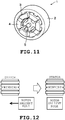
- FIG.11 is a perspective view illustrating the structure of an SR motor.
- An SR motor 1 is provided with a plurality of salient poles 3 protruding toward the inner peripheral side of a stator core 2 having a substantially annular cross section. Windings 4 for each of the phases are wound around the salient poles 3.
- a rotor core 5 having a substantially cruciform cross section is disposed in a hollow portion of the stator core 2.
- the SR motor 1 exhibits a doubly salient pole structure having protrusions and recesses on both the stator core 2 and the rotor core 5.
- FIG.12 is an explanatory diagram on the operation of the SR motor.
- torque and rotational force are exerted in the direction to align the salient poles in the stator side with the salient poles in the rotor side.
- Magnetic resistance is minimized and torque amounts to zero when the salient poles of the two sides are aligned.
- a mechanical action that works to reduce the magnetic resistance is exerted on the energized salient poles.
- Torque T of the SR motor is generally expressed by the following equation (1).
- T I 2 / 2 dL / d ⁇
- T torque
- I current
- L inductance
- ⁇ rotor position
- FIG. 13 illustrates the relation between inductance and the rotor position of an SR motor having 6 stator poles and 4 rotor poles.
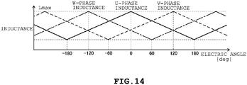
- FIG.14 shows how the inductance of each phase varies with the variation of the electric angle.
- FIG.7 shows a general drive circuit of an SR motor.
- a drive circuit 11 of the SR motor includes a positive side switch S1 (S1U, S1V, S1W) and a negative side switch S2 (S2X, S2Y, S2Z) for each of the U phase, V phase, and the W phase.
- One end of the positive side switch S1 is connected to a positive terminal of a direct-current (DC) power supply 12 and one end of the negative side switch S2 is connected to a negative terminal of a DC power supply 12.
- Windings 4 of each of the phases are connected between the other ends of the switches S1 and S2.
- Switches S1 and S2 are configured by a semiconductor element such as a MOSFET.
- the cathode of a diode D1 (D1U, D1V, D1W) is connected to the positive terminal of the DC power supply 12 and the anode of the diode D1 is connected to the other end of the switch S2.
- the anode of a diode D2 (D2X, D2Y, D2Z) is connected to a negative terminal of the DC power supply 12 and the cathode of the diode D2 is connected to the other end of the switch S1.
- FIGS.8 to 10 indicate energization modes of the drive circuit 11.
- positive voltage is applied to the windings 4 to cause conduction of current when the switches S1 and S2 in the upper side and the lower side are turned on.
- back flow current flows via the diode D2 in the lower side.
- negative voltage is applied to the windings via the diodes D1 and D2 in the upper side and the lower side to cause current to be regenerated to the power supply.
- FIG. 1 is a functional block diagram illustrating the main portion of a motor control device 13.
- the motor control device 13 includes a rectangular wave output portion 14 and a PWM (Pulse Width Modulation) output portion 15 for generating drive signals to be outputted to the drive circuit 11.
- PWM Pulse Width Modulation
- the rectangular wave output portion 14 generates a rectangular wave signal by comparing the reference value of the waveform to be outputted which is given by a CPU not shown with the electric angle of the SR motor 1.
- the reference values A and N set to a comparator 16 correspond to the electric angle at the start point of output of the rectangular wave signal and the electric angle at the end point of output of the rectangular wave signal, respectively. That is, by providing reference values A and N, it is possible to specify the output period of the rectangular wave signal.
- the reference values A, B, and C set to comparators 17B and 17C determine the pulse waveform outputted in the aforementioned output period.
- the output signals of the comparators 16, 17B, and 17C are all inputted to a waveform synthesizer 18 and the waveform synthesizer 18 outputs a rectangular wave signal SNCU by taking an exclusive OR of the inputted signals.
- reference values B and C are set so that A ⁇ B and C ⁇ N as indicated in FIG. 3 .
- signals QUBOV and QUCOV outputted from the comparator 17 at electric angle A are raised.
- Rectangular wave signal SNCU outputted from the waveform synthesizer 18 is also raised.
- the rectangular wave signal SNCU falls as well. Then, when the signal QUCOV falls at electric angle C, the rectangular wave signal SNCU rises and when the signal QUCOV falls at electric angle N, the rectangular wave signal SNCU falls as well. As a result of the input signals being synthesized at the waveform synthesizer 18, the rectangular wave signal SNCU exhibits a waveform which turns to a high level in the ranges spanning between electric angle A and B and between electric angle C and N.
- the rectangular wave output portion 14 is capable of outputting different waveforms when outputting plural rectangular wave pulses in 1 drive period by individually setting the rise and fall timings for each phase.
- the PWM output portion 15 is provided with a counter 19 that generates a saw-tooth wave serving as a PWM carrier.
- the count value of the counter 19 is inputted to a subtractor 20 and a data latch 21.
- the data latch 21 uses the rising edge of the QUNOV signal outputted from the comparator 16 of the rectangular wave output portion 14 as a trigger for latching the inputted count value.
- the subtractor 20 subtracts the count value latched by the data latch 21 from the count value of the counter 19 and inputs the difference to the comparator 22.
- the data value of the carrier outputted via the subtractor 20 amounts to zero at the timing when the output of the rectangular wave signal is started.
- the comparator 22 generates a PWM signal SRU by comparing the data value of the above described carrier and the duty reference value set by the CPU and inputs the signal SRU to one of the input terminals of the AND gate 23.
- the signal QUNOV is inputted to the other input terminal of the AND gate 23.
- the PWM signal SRU is outputted during the period in which the signal QUNOV indicates the high level.
- FIG.2 illustrates one example of a PWM signal outputted from a U terminal.
- Three selectors 24, 25, and 26 are disposed in the output side of the AND gate 23.
- the output signal (0) of the AND gate 23 and the rectangular wave signal SNCU (1) are inputted to the selector 24 and the output signal (0) of the selector 24 and the signal QUNOV (1) are inputted to the selectors 25 and 26.
- the selector 25 outputs a control signal to the switch S1U in the upper side U phase of the drive circuit 11 and the selector 26 outputs a control signal to the switch S2X in the lower side U phase of the drive circuit 11.
- the selector 24 selects the PWM signal SRU when the output mode is "PWM” and the selection signal is “0” and selects the rectangular wave signal SNCU when the output mode is “rectangular wave” and the selection signal is “1".
- the selector 25 selects the selector 24 side when the output mode is “upper side back flow” and the selection signal is “0” and selects the signal QUNOV when the output mode is not “upper side back flow” and the selection signal is "1".
- the selector 26 selects the selector 24 side when the output mode is "lower side back flow” and the selection signal is "0” and selects the signal QUNOV when the output mode is not “lower side back flow” and the selection signal is "1".
- the back flow mode illustrated in FIG.9 is not executed.
- the back flow mode is to be executed in the output modes R (2) and R (3), only 1 pulse spanning across the signal output period is outputted to either of the upper side or the lower side by the rectangular wave output portion 14.
- the timing of the initial rising of the PWM signal is synchronized with the rising of the rectangular wave signal generated by the rectangular wave output portion 14.
- the switching of the output mode may also be done by the CPU. However, the switching may be conducted automatically through hardware configuration by comparing the PWM frequency, the electric angle period, and the pulse count of the rectangular wave output.
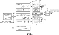
- FIG.4 is a functional block diagram illustrating the configuration of a drive signal switcher 31.
- FIG.5 is a flowchart describing the operations performed by the configuration illustrated in FIG.4 .
- the drive signal switcher 31 is provided with capture portions 33A and 33B and a free counter 32.
- the capture portions 33A and 33B capture the count value of the free counter 32 and are both provided with a current value register 34, a previous value register 35, and a subtractor 36.
- the capture portion 33A when the count value of the PWM carrier reaches the maximum value, data is transferred from the current value register 34 to the previous value register 35 and the count value of the free counter 32 is stored in the current value register 34.
- the subtractor 36 subtracts the register value of the previous value register 35 from the register value of the current value register 34.
- the capture portion 33A captures the count data corresponding to the frequency of the PWM carrier (S1) in the above described manner.
- the capture portion 33B On the other hand, data value indicating the rotational angle and the electric angle of the SR motor 1 is multiplied by the pulse count of the rectangular wave signal generated by the rectangular wave output portion 14 using a multiplier 37 to generate multiplication waveform data. Then, in the capture portion 33B, when the count value of the multiplication waveform data reaches the maximum value, data is transferred from the current value register 34 to the previous value register 35 and the count value of the free counter 32 is stored in the current value register 34. Thus, the capture portion 33B captures count data corresponding to (motor rotational angle) ⁇ (rectangular wave pulse count) (S2) .
- the output data of the capture portions 33A and 33B is inputted to a magnitude comparator 38.
- the magnitude comparator 38 outputs a signal "1" for selecting the rectangular wave mode when capture data B is equal to or less than capture data A (S3: YES) (S4) and outputs a signal "0" for selecting the PWM mode when the capture data B is greater than capture data A (S3: NO) (S5).
- the capture portions 33A and 33B and the comparator 38 correspond to a frequency comparator.
- the energization phase needs to be switched 24 times per 1 rotation.
- pulse count in 1 energization period is 7 and the PWM frequency is 20 kHz
- FIG.15 illustrates the waveforms being outputted in the case where the PWM signal and the rectangular wave signal are not synchronized and the PWM carrier is the same for all of the phases.
- the rise timing of the actual phase current is delayed from the proper rise timing because of the delay in the timing to start output of the PWM signal.
- the timing to start output of the PWM signal coincides with the timing to start output of the rectangular wave signal as illustrated in FIG.16 since the PWM carrier of each phase is reset at the timing to start output of the rectangular wave signal and the timing when the reference excitation angle is given. This eliminates the delay in the rising of phase current which has been exemplified in FIG.15 . It is to be noted that "reference" indicated in the figures correspond to the duty reference value.
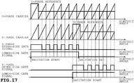
- FIG.17 illustrates output mode P(2) and executes the back flow mode while the upper side is turned off.
- FIG.18 illustrates the output mode P(1) which does not execute the back flow mode.
- FIG.19 represents a case in which the output pulse count is set to "1" in output mode R (1) and illustrates a waveform in which 1 pulse of rectangular wave is outputted having an advance angle of 0 degrees and an energization angle of 120 degrees.
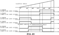
- FIG.20 represents the same output mode as FIG.19 and illustrates a waveform in which 1 pulse of rectangular wave is outputted having an advance angle of 30 degrees and an energization angle of 150 degrees.
- FIG. 21 illustrates a waveform of output mode R (2) having an advance angle 30 degrees.
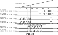
- FIG.22 illustrates a waveform of output mode R (1) having an advance angle 30 degrees.
- FIG.23 illustrates the current waveforms being outputted when rectangular wave pulses having the same waveform are outputted in the case where inductances differ in the windings of each phase.
- the inclinations of the inductances are the same and thus, the torque generated in the V phase becomes smaller than the torque generated in the U phase.
- the PWM generator 15 generates a PWM signal to be outputted to the drive circuit 11 that energizes the windings of the SR motor 1 and the rectangular wave generator 14 outputs a rectangular wave signal of 1 pulse or more to the drive circuit 11 in 1 drive period of each phase based on the rotational position of the SR motor 1.
- the PWM generator 15 synchronizes the timing for starting the generation of the carrier of the PWM signal with the rising of the rectangular wave signal.
- the drive signal switcher 31 executes switching so that a PWM drive by the PWM signal is performed when the rotational speed of the SR motor 1 is equal to or less than the threshold value and the rectangular wave drive by the rectangular wave signal is performed when the rotational speed of the SR motor 1 is greater than the threshold value.
- the drive signal switcher 31 is provided with the capture portions 33A and 33B and the comparator 38 that compare the frequency obtained by multiplying the electric angle frequency of the SR motor 1 by the pulse count of the rectangular wave signal outputted by the rectangular wave generator 14 with the frequency of the PWM carrier.
- the drive signal switcher 31 switches the drive methods based on the result of comparison. It is thus, possible to appropriately evaluate the rotation count in which the switching of drive methods is performed based on the pulse count of the rectangular wave signal.
- the rectangular wave generator 14 is rendered capable of setting the pulse waveform to be outputted in 1 drive period independently for each phase. It is thus, possible to suppress torque ripple originating from variation of inductance among the phases. Further, the rectangular wave generator 14 outputs only 1 pulse in 1 drive period while the PWM drive is selected by the drive signal switcher 31. It is thus, possible to prevent generation of multiple unnecessary rectangular wave pulses.
- the number of salient poles of the SR motor 1 and the frequency of the PWM carrier, etc. may be modified depending upon design requirements.
- the configuration of enabling the rectangular wave generator 14 to set the pulse waveform to be outputted in 1 drive period independently for each phase may be employed on a required basis.
- the synchronization of the timing to start generation of the carrier of the PWM signal with the rising of the rectangular wave signal may alternatively be realized by causing the counter 19 to start counting or to be reset at the timing in which the output of the rectangular wave signal is started.
Landscapes
- Engineering & Computer Science (AREA)
- Power Engineering (AREA)
- Control Of Electric Motors In General (AREA)
- Control Of Motors That Do Not Use Commutators (AREA)
- Control Of Stepping Motors (AREA)
Applications Claiming Priority (1)
| Application Number | Priority Date | Filing Date | Title |
|---|---|---|---|
| JP2016147334A JP6591368B2 (ja) | 2016-07-27 | 2016-07-27 | モータ制御用デバイス |
Publications (1)
| Publication Number | Publication Date |
|---|---|
| EP3276818A1 true EP3276818A1 (de) | 2018-01-31 |
Family
ID=59387974
Family Applications (1)
| Application Number | Title | Priority Date | Filing Date |
|---|---|---|---|
| EP17182760.3A Withdrawn EP3276818A1 (de) | 2016-07-27 | 2017-07-24 | Motorsteuerungsvorrichtung |
Country Status (4)
| Country | Link |
|---|---|
| US (1) | US10630221B2 (de) |
| EP (1) | EP3276818A1 (de) |
| JP (1) | JP6591368B2 (de) |
| CN (1) | CN107666265B (de) |
Families Citing this family (3)
| Publication number | Priority date | Publication date | Assignee | Title |
|---|---|---|---|---|
| CN108429509B (zh) * | 2018-03-15 | 2019-08-30 | 合肥工业大学 | 开关磁阻电机分段pwm占空比控制方法 |
| JP7094859B2 (ja) * | 2018-11-15 | 2022-07-04 | 澤藤電機株式会社 | モータ制御装置及びモータ制御方法 |
| CN110120762B (zh) * | 2019-05-23 | 2021-04-27 | 合肥工业大学 | 无误差的开关磁阻电机电流控制方法 |
Citations (6)
| Publication number | Priority date | Publication date | Assignee | Title |
|---|---|---|---|---|
| WO1990016111A1 (en) * | 1989-06-15 | 1990-12-27 | Aktiebolaget Electrolux | A device for controlling a reluctance motor |
| EP0736962A2 (de) * | 1995-04-04 | 1996-10-09 | Switched Reluctance Drives Ltd | Steuergerät für eine geschaltete Reluktanzmaschine |
| JPH09182490A (ja) | 1995-12-26 | 1997-07-11 | Aisin Seiki Co Ltd | スイッチドリラクタンスモータの制御装置 |
| JP2009112140A (ja) * | 2007-10-31 | 2009-05-21 | Nissan Motor Co Ltd | 電動機の制御装置およびその制御方法 |
| WO2011161408A2 (en) * | 2010-06-22 | 2011-12-29 | Aeristech Control Technologies Limited | Controller |
| JP2012125096A (ja) * | 2010-12-10 | 2012-06-28 | Daihatsu Motor Co Ltd | モータ駆動制御装置 |
Family Cites Families (11)
| Publication number | Priority date | Publication date | Assignee | Title |
|---|---|---|---|---|
| US4123692A (en) * | 1976-10-26 | 1978-10-31 | Allis-Chalmers Corporation | Adjustable speed electric motor drive having constant harmonic content |
| JP3803781B2 (ja) * | 1997-05-30 | 2006-08-02 | アイシン精機株式会社 | 電気モ−タの通電制御装置 |
| JP2000023481A (ja) * | 1998-06-30 | 2000-01-21 | Mitsubishi Electric Corp | Pwm制御回路装置 |
| US7608964B2 (en) * | 2004-03-31 | 2009-10-27 | Daikin Industries, Ltd. | Motor, blower, compressor, and air conditioner |
| JP4802696B2 (ja) * | 2005-12-15 | 2011-10-26 | 日産自動車株式会社 | モータ制御装置 |
| JP2010246336A (ja) * | 2009-04-09 | 2010-10-28 | Toyota Industries Corp | モータ制御装置およびモータ制御方法 |
| US8624534B2 (en) * | 2009-06-22 | 2014-01-07 | Aisin Aw Co., Ltd. | Control device for electric motor driving apparatus |
| CN102468793B (zh) * | 2010-11-08 | 2015-04-22 | 台达电子工业股份有限公司 | 风扇转速控制装置 |
| JP2012157135A (ja) * | 2011-01-25 | 2012-08-16 | Nidec Techno Motor Corp | モータの制御装置 |
| TWI504136B (zh) * | 2013-10-25 | 2015-10-11 | Ind Tech Res Inst | 雙模式驅動方法及裝置 |
| JP6338902B2 (ja) * | 2014-03-24 | 2018-06-06 | Ntn株式会社 | 電動ブレーキ装置および電動ブレーキ装置システム |
-
2016
- 2016-07-27 JP JP2016147334A patent/JP6591368B2/ja active Active
-
2017
- 2017-07-24 EP EP17182760.3A patent/EP3276818A1/de not_active Withdrawn
- 2017-07-25 US US15/658,886 patent/US10630221B2/en active Active
- 2017-07-26 CN CN201710616237.6A patent/CN107666265B/zh active Active
Patent Citations (6)
| Publication number | Priority date | Publication date | Assignee | Title |
|---|---|---|---|---|
| WO1990016111A1 (en) * | 1989-06-15 | 1990-12-27 | Aktiebolaget Electrolux | A device for controlling a reluctance motor |
| EP0736962A2 (de) * | 1995-04-04 | 1996-10-09 | Switched Reluctance Drives Ltd | Steuergerät für eine geschaltete Reluktanzmaschine |
| JPH09182490A (ja) | 1995-12-26 | 1997-07-11 | Aisin Seiki Co Ltd | スイッチドリラクタンスモータの制御装置 |
| JP2009112140A (ja) * | 2007-10-31 | 2009-05-21 | Nissan Motor Co Ltd | 電動機の制御装置およびその制御方法 |
| WO2011161408A2 (en) * | 2010-06-22 | 2011-12-29 | Aeristech Control Technologies Limited | Controller |
| JP2012125096A (ja) * | 2010-12-10 | 2012-06-28 | Daihatsu Motor Co Ltd | モータ駆動制御装置 |
Also Published As
| Publication number | Publication date |
|---|---|
| US10630221B2 (en) | 2020-04-21 |
| JP2018019496A (ja) | 2018-02-01 |
| JP6591368B2 (ja) | 2019-10-16 |
| US20180034400A1 (en) | 2018-02-01 |
| CN107666265B (zh) | 2020-05-05 |
| CN107666265A (zh) | 2018-02-06 |
Similar Documents
| Publication | Publication Date | Title |
|---|---|---|
| EP2625778B1 (de) | Regelung eines elektromotors | |
| US9431931B2 (en) | Controller for a brushless motor | |
| EP2704306B1 (de) | Vorrichtung zur Steuerung eines Motors für ein Elektrofahrzeug und Verfahren zur Verminderung der Drehmomentschwankung damit | |
| JP4959460B2 (ja) | モータ起動装置及びモータ起動方法 | |
| US9960722B2 (en) | Motor controller | |
| JP2011211799A (ja) | モータ駆動装置 | |
| JP2012196725A (ja) | 電動工具 | |
| Bharatkar et al. | Dual-mode switching technique for reduction of commutation torque ripple of brushless dc motor | |
| US10630221B2 (en) | Motor control device | |
| EP3644494B1 (de) | Thyristorstartvorrichtung | |
| US10951144B2 (en) | Thyristor starter | |
| EP3550718B1 (de) | Fahrsteuerungsvorrichtung und fahrsteuerungsverfahren | |
| JP2012191728A (ja) | モータの制御装置 | |
| EP3644498B1 (de) | Thyristor-starter | |
| JP6198083B2 (ja) | 電動工具 | |
| KR20210073596A (ko) | 무브러시 영구 자석 모터의 제어 방법 | |
| WO2018047236A1 (ja) | モータ駆動装置 | |
| JP2012191729A (ja) | モータの制御装置 | |
| JP2016226084A (ja) | スイッチトリラクタンスモータの制御装置 | |
| JP2018042393A (ja) | モータ駆動制御装置 | |
| JP2012191730A (ja) | モータの制御装置 |
Legal Events
| Date | Code | Title | Description |
|---|---|---|---|
| PUAI | Public reference made under article 153(3) epc to a published international application that has entered the european phase |
Free format text: ORIGINAL CODE: 0009012 |
|
| STAA | Information on the status of an ep patent application or granted ep patent |
Free format text: STATUS: REQUEST FOR EXAMINATION WAS MADE |
|
| 17P | Request for examination filed |
Effective date: 20170724 |
|
| AK | Designated contracting states |
Kind code of ref document: A1 Designated state(s): AL AT BE BG CH CY CZ DE DK EE ES FI FR GB GR HR HU IE IS IT LI LT LU LV MC MK MT NL NO PL PT RO RS SE SI SK SM TR |
|
| AX | Request for extension of the european patent |
Extension state: BA ME |
|
| STAA | Information on the status of an ep patent application or granted ep patent |
Free format text: STATUS: EXAMINATION IS IN PROGRESS |
|
| 17Q | First examination report despatched |
Effective date: 20200205 |
|
| GRAP | Despatch of communication of intention to grant a patent |
Free format text: ORIGINAL CODE: EPIDOSNIGR1 |
|
| STAA | Information on the status of an ep patent application or granted ep patent |
Free format text: STATUS: GRANT OF PATENT IS INTENDED |
|
| RIC1 | Information provided on ipc code assigned before grant |
Ipc: H02M 7/5395 20060101ALN20221018BHEP Ipc: H02P 25/098 20160101AFI20221018BHEP |
|
| INTG | Intention to grant announced |
Effective date: 20221031 |
|
| STAA | Information on the status of an ep patent application or granted ep patent |
Free format text: STATUS: THE APPLICATION IS DEEMED TO BE WITHDRAWN |
|
| 18D | Application deemed to be withdrawn |
Effective date: 20230311 |