EP3276807B1 - Power conversion device - Google Patents
Power conversion device Download PDFInfo
- Publication number
- EP3276807B1 EP3276807B1 EP16817509.9A EP16817509A EP3276807B1 EP 3276807 B1 EP3276807 B1 EP 3276807B1 EP 16817509 A EP16817509 A EP 16817509A EP 3276807 B1 EP3276807 B1 EP 3276807B1
- Authority
- EP
- European Patent Office
- Prior art keywords
- line
- power converter
- conductive member
- connecting line
- heatsink
- Prior art date
- Legal status (The legal status is an assumption and is not a legal conclusion. Google has not performed a legal analysis and makes no representation as to the accuracy of the status listed.)
- Active
Links
- 238000006243 chemical reaction Methods 0.000 title description 4
- 239000012212 insulator Substances 0.000 claims description 15
- 238000003780 insertion Methods 0.000 claims description 9
- 230000037431 insertion Effects 0.000 claims description 9
- 238000010521 absorption reaction Methods 0.000 claims description 2
- 230000005855 radiation Effects 0.000 claims description 2
- 239000004065 semiconductor Substances 0.000 description 52
- 230000003071 parasitic effect Effects 0.000 description 21
- 238000010586 diagram Methods 0.000 description 16
- 230000002123 temporal effect Effects 0.000 description 11
- 239000010409 thin film Substances 0.000 description 8
- 239000010408 film Substances 0.000 description 7
- 230000000638 stimulation Effects 0.000 description 7
- 241001510512 Chlamydia phage 2 Species 0.000 description 6
- 239000003990 capacitor Substances 0.000 description 6
- 101150009410 Chp2 gene Proteins 0.000 description 5
- 239000012774 insulation material Substances 0.000 description 5
- 238000000034 method Methods 0.000 description 5
- 241000839426 Chlamydia virus Chp1 Species 0.000 description 4
- 101150071546 Chp1 gene Proteins 0.000 description 4
- 230000000694 effects Effects 0.000 description 4
- 239000000919 ceramic Substances 0.000 description 3
- 238000002955 isolation Methods 0.000 description 3
- RYGMFSIKBFXOCR-UHFFFAOYSA-N Copper Chemical compound [Cu] RYGMFSIKBFXOCR-UHFFFAOYSA-N 0.000 description 2
- 230000005856 abnormality Effects 0.000 description 2
- 238000001816 cooling Methods 0.000 description 2
- 238000009413 insulation Methods 0.000 description 2
- 238000005452 bending Methods 0.000 description 1
- 239000011889 copper foil Substances 0.000 description 1
- 230000005669 field effect Effects 0.000 description 1
- 238000009499 grossing Methods 0.000 description 1
- 238000004519 manufacturing process Methods 0.000 description 1
- 239000000463 material Substances 0.000 description 1
- 239000011347 resin Substances 0.000 description 1
- 229920005989 resin Polymers 0.000 description 1
Images


Classifications
-
- H—ELECTRICITY
- H05—ELECTRIC TECHNIQUES NOT OTHERWISE PROVIDED FOR
- H05K—PRINTED CIRCUITS; CASINGS OR CONSTRUCTIONAL DETAILS OF ELECTRIC APPARATUS; MANUFACTURE OF ASSEMBLAGES OF ELECTRICAL COMPONENTS
- H05K1/00—Printed circuits
- H05K1/02—Details
- H05K1/0213—Electrical arrangements not otherwise provided for
- H05K1/0216—Reduction of cross-talk, noise or electromagnetic interference
-
- H—ELECTRICITY
- H01—ELECTRIC ELEMENTS
- H01L—SEMICONDUCTOR DEVICES NOT COVERED BY CLASS H10
- H01L23/00—Details of semiconductor or other solid state devices
- H01L23/34—Arrangements for cooling, heating, ventilating or temperature compensation ; Temperature sensing arrangements
- H01L23/36—Selection of materials, or shaping, to facilitate cooling or heating, e.g. heatsinks
-
- H—ELECTRICITY
- H01—ELECTRIC ELEMENTS
- H01L—SEMICONDUCTOR DEVICES NOT COVERED BY CLASS H10
- H01L23/00—Details of semiconductor or other solid state devices
- H01L23/34—Arrangements for cooling, heating, ventilating or temperature compensation ; Temperature sensing arrangements
- H01L23/42—Fillings or auxiliary members in containers or encapsulations selected or arranged to facilitate heating or cooling
- H01L23/433—Auxiliary members in containers characterised by their shape, e.g. pistons
- H01L23/4332—Bellows
-
- H—ELECTRICITY
- H01—ELECTRIC ELEMENTS
- H01L—SEMICONDUCTOR DEVICES NOT COVERED BY CLASS H10
- H01L23/00—Details of semiconductor or other solid state devices
- H01L23/52—Arrangements for conducting electric current within the device in operation from one component to another, i.e. interconnections, e.g. wires, lead frames
- H01L23/522—Arrangements for conducting electric current within the device in operation from one component to another, i.e. interconnections, e.g. wires, lead frames including external interconnections consisting of a multilayer structure of conductive and insulating layers inseparably formed on the semiconductor body
- H01L23/5222—Capacitive arrangements or effects of, or between wiring layers
-
- H—ELECTRICITY
- H02—GENERATION; CONVERSION OR DISTRIBUTION OF ELECTRIC POWER
- H02M—APPARATUS FOR CONVERSION BETWEEN AC AND AC, BETWEEN AC AND DC, OR BETWEEN DC AND DC, AND FOR USE WITH MAINS OR SIMILAR POWER SUPPLY SYSTEMS; CONVERSION OF DC OR AC INPUT POWER INTO SURGE OUTPUT POWER; CONTROL OR REGULATION THEREOF
- H02M1/00—Details of apparatus for conversion
- H02M1/12—Arrangements for reducing harmonics from ac input or output
- H02M1/123—Suppression of common mode voltage or current
-
- H—ELECTRICITY
- H02—GENERATION; CONVERSION OR DISTRIBUTION OF ELECTRIC POWER
- H02M—APPARATUS FOR CONVERSION BETWEEN AC AND AC, BETWEEN AC AND DC, OR BETWEEN DC AND DC, AND FOR USE WITH MAINS OR SIMILAR POWER SUPPLY SYSTEMS; CONVERSION OF DC OR AC INPUT POWER INTO SURGE OUTPUT POWER; CONTROL OR REGULATION THEREOF
- H02M1/00—Details of apparatus for conversion
- H02M1/44—Circuits or arrangements for compensating for electromagnetic interference in converters or inverters
-
- H—ELECTRICITY
- H02—GENERATION; CONVERSION OR DISTRIBUTION OF ELECTRIC POWER
- H02M—APPARATUS FOR CONVERSION BETWEEN AC AND AC, BETWEEN AC AND DC, OR BETWEEN DC AND DC, AND FOR USE WITH MAINS OR SIMILAR POWER SUPPLY SYSTEMS; CONVERSION OF DC OR AC INPUT POWER INTO SURGE OUTPUT POWER; CONTROL OR REGULATION THEREOF
- H02M3/00—Conversion of dc power input into dc power output
- H02M3/003—Constructional details, e.g. physical layout, assembly, wiring or busbar connections
-
- H—ELECTRICITY
- H02—GENERATION; CONVERSION OR DISTRIBUTION OF ELECTRIC POWER
- H02M—APPARATUS FOR CONVERSION BETWEEN AC AND AC, BETWEEN AC AND DC, OR BETWEEN DC AND DC, AND FOR USE WITH MAINS OR SIMILAR POWER SUPPLY SYSTEMS; CONVERSION OF DC OR AC INPUT POWER INTO SURGE OUTPUT POWER; CONTROL OR REGULATION THEREOF
- H02M3/00—Conversion of dc power input into dc power output
- H02M3/02—Conversion of dc power input into dc power output without intermediate conversion into ac
- H02M3/04—Conversion of dc power input into dc power output without intermediate conversion into ac by static converters
- H02M3/10—Conversion of dc power input into dc power output without intermediate conversion into ac by static converters using discharge tubes with control electrode or semiconductor devices with control electrode
- H02M3/145—Conversion of dc power input into dc power output without intermediate conversion into ac by static converters using discharge tubes with control electrode or semiconductor devices with control electrode using devices of a triode or transistor type requiring continuous application of a control signal
- H02M3/155—Conversion of dc power input into dc power output without intermediate conversion into ac by static converters using discharge tubes with control electrode or semiconductor devices with control electrode using devices of a triode or transistor type requiring continuous application of a control signal using semiconductor devices only
- H02M3/156—Conversion of dc power input into dc power output without intermediate conversion into ac by static converters using discharge tubes with control electrode or semiconductor devices with control electrode using devices of a triode or transistor type requiring continuous application of a control signal using semiconductor devices only with automatic control of output voltage or current, e.g. switching regulators
-
- H—ELECTRICITY
- H02—GENERATION; CONVERSION OR DISTRIBUTION OF ELECTRIC POWER
- H02M—APPARATUS FOR CONVERSION BETWEEN AC AND AC, BETWEEN AC AND DC, OR BETWEEN DC AND DC, AND FOR USE WITH MAINS OR SIMILAR POWER SUPPLY SYSTEMS; CONVERSION OF DC OR AC INPUT POWER INTO SURGE OUTPUT POWER; CONTROL OR REGULATION THEREOF
- H02M7/00—Conversion of ac power input into dc power output; Conversion of dc power input into ac power output
- H02M7/42—Conversion of dc power input into ac power output without possibility of reversal
- H02M7/44—Conversion of dc power input into ac power output without possibility of reversal by static converters
- H02M7/48—Conversion of dc power input into ac power output without possibility of reversal by static converters using discharge tubes with control electrode or semiconductor devices with control electrode
-
- H—ELECTRICITY
- H05—ELECTRIC TECHNIQUES NOT OTHERWISE PROVIDED FOR
- H05K—PRINTED CIRCUITS; CASINGS OR CONSTRUCTIONAL DETAILS OF ELECTRIC APPARATUS; MANUFACTURE OF ASSEMBLAGES OF ELECTRICAL COMPONENTS
- H05K1/00—Printed circuits
- H05K1/18—Printed circuits structurally associated with non-printed electric components
- H05K1/181—Printed circuits structurally associated with non-printed electric components associated with surface mounted components
-
- H—ELECTRICITY
- H05—ELECTRIC TECHNIQUES NOT OTHERWISE PROVIDED FOR
- H05K—PRINTED CIRCUITS; CASINGS OR CONSTRUCTIONAL DETAILS OF ELECTRIC APPARATUS; MANUFACTURE OF ASSEMBLAGES OF ELECTRICAL COMPONENTS
- H05K1/00—Printed circuits
- H05K1/02—Details
- H05K1/0201—Thermal arrangements, e.g. for cooling, heating or preventing overheating
- H05K1/0203—Cooling of mounted components
- H05K1/0209—External configuration of printed circuit board adapted for heat dissipation, e.g. lay-out of conductors, coatings
-
- H—ELECTRICITY
- H05—ELECTRIC TECHNIQUES NOT OTHERWISE PROVIDED FOR
- H05K—PRINTED CIRCUITS; CASINGS OR CONSTRUCTIONAL DETAILS OF ELECTRIC APPARATUS; MANUFACTURE OF ASSEMBLAGES OF ELECTRICAL COMPONENTS
- H05K2201/00—Indexing scheme relating to printed circuits covered by H05K1/00
- H05K2201/03—Conductive materials
- H05K2201/0302—Properties and characteristics in general
- H05K2201/0311—Metallic part with specific elastic properties, e.g. bent piece of metal as electrical contact
-
- H—ELECTRICITY
- H05—ELECTRIC TECHNIQUES NOT OTHERWISE PROVIDED FOR
- H05K—PRINTED CIRCUITS; CASINGS OR CONSTRUCTIONAL DETAILS OF ELECTRIC APPARATUS; MANUFACTURE OF ASSEMBLAGES OF ELECTRICAL COMPONENTS
- H05K2201/00—Indexing scheme relating to printed circuits covered by H05K1/00
- H05K2201/06—Thermal details
- H05K2201/066—Heatsink mounted on the surface of the PCB
-
- H—ELECTRICITY
- H05—ELECTRIC TECHNIQUES NOT OTHERWISE PROVIDED FOR
- H05K—PRINTED CIRCUITS; CASINGS OR CONSTRUCTIONAL DETAILS OF ELECTRIC APPARATUS; MANUFACTURE OF ASSEMBLAGES OF ELECTRICAL COMPONENTS
- H05K2201/00—Indexing scheme relating to printed circuits covered by H05K1/00
- H05K2201/07—Electric details
- H05K2201/0776—Resistance and impedance
- H05K2201/0792—Means against parasitic impedance; Means against eddy currents
-
- H—ELECTRICITY
- H05—ELECTRIC TECHNIQUES NOT OTHERWISE PROVIDED FOR
- H05K—PRINTED CIRCUITS; CASINGS OR CONSTRUCTIONAL DETAILS OF ELECTRIC APPARATUS; MANUFACTURE OF ASSEMBLAGES OF ELECTRICAL COMPONENTS
- H05K2201/00—Indexing scheme relating to printed circuits covered by H05K1/00
- H05K2201/10—Details of components or other objects attached to or integrated in a printed circuit board
- H05K2201/10007—Types of components
- H05K2201/10166—Transistor
-
- H—ELECTRICITY
- H05—ELECTRIC TECHNIQUES NOT OTHERWISE PROVIDED FOR
- H05K—PRINTED CIRCUITS; CASINGS OR CONSTRUCTIONAL DETAILS OF ELECTRIC APPARATUS; MANUFACTURE OF ASSEMBLAGES OF ELECTRICAL COMPONENTS
- H05K2201/00—Indexing scheme relating to printed circuits covered by H05K1/00
- H05K2201/10—Details of components or other objects attached to or integrated in a printed circuit board
- H05K2201/10227—Other objects, e.g. metallic pieces
- H05K2201/10265—Metallic coils or springs, e.g. as part of a connection element
-
- H—ELECTRICITY
- H05—ELECTRIC TECHNIQUES NOT OTHERWISE PROVIDED FOR
- H05K—PRINTED CIRCUITS; CASINGS OR CONSTRUCTIONAL DETAILS OF ELECTRIC APPARATUS; MANUFACTURE OF ASSEMBLAGES OF ELECTRICAL COMPONENTS
- H05K2201/00—Indexing scheme relating to printed circuits covered by H05K1/00
- H05K2201/10—Details of components or other objects attached to or integrated in a printed circuit board
- H05K2201/10227—Other objects, e.g. metallic pieces
- H05K2201/10356—Cables
-
- H—ELECTRICITY
- H05—ELECTRIC TECHNIQUES NOT OTHERWISE PROVIDED FOR
- H05K—PRINTED CIRCUITS; CASINGS OR CONSTRUCTIONAL DETAILS OF ELECTRIC APPARATUS; MANUFACTURE OF ASSEMBLAGES OF ELECTRICAL COMPONENTS
- H05K2201/00—Indexing scheme relating to printed circuits covered by H05K1/00
- H05K2201/10—Details of components or other objects attached to or integrated in a printed circuit board
- H05K2201/10613—Details of electrical connections of non-printed components, e.g. special leads
- H05K2201/10621—Components characterised by their electrical contacts
- H05K2201/10628—Leaded surface mounted device
-
- H—ELECTRICITY
- H05—ELECTRIC TECHNIQUES NOT OTHERWISE PROVIDED FOR
- H05K—PRINTED CIRCUITS; CASINGS OR CONSTRUCTIONAL DETAILS OF ELECTRIC APPARATUS; MANUFACTURE OF ASSEMBLAGES OF ELECTRICAL COMPONENTS
- H05K2201/00—Indexing scheme relating to printed circuits covered by H05K1/00
- H05K2201/10—Details of components or other objects attached to or integrated in a printed circuit board
- H05K2201/10613—Details of electrical connections of non-printed components, e.g. special leads
- H05K2201/10742—Details of leads
- H05K2201/1075—Shape details
- H05K2201/10757—Bent leads
Definitions
- the present invention relates to a power converter equipped with a line provided on a circuit board, a switching element provided on the circuit board and connected to the line, and a radiator provided on the circuit board.
- a power converter is used in various applications, in which a semiconductor switch is switched to control an output voltage and/or an output current. To the power converter is attached a heatsink to radiate heat generated by the semiconductor switch.
- Fig. 1 is a schematic side view schematically showing a semiconductor switch equipped on a power converter and an outer appearance of an attached heatsink.
- Fig. 1 shows a semiconductor switch SW equipped on the power converter.
- the semiconductor switch SW is attached with a heatsink HS and is fixed on a circuit board B.
- the heatsink HS has a function of cooling by externally radiating heat generated on the semiconductor switch SW.
- Fig. 2 is an explanatory diagram schematically depicting the heatsink in a circuit diagram related to the semiconductor switch equipped on the power converter.
- Fig. 2 shows a circuit in which the semiconductor switch SW is provided to short-circuit between a pair of lines connecting an input side and an output side, and the heatsink HS is shown on the right side of the semiconductor switch SW.
- the heatsink HS is connected to the FG.
- a parasitic capacitance Chp is generated between the semiconductor switch SW and the heatsink HS.
- the generated parasitic capacitance Chp transfers to the FG a voltage fluctuation at a point P1 connected to the positive terminal of the semiconductor switch SW, and whereby a common mode current Icm flows as noise.
- Fig. 3 is a graph showing a voltage change at the point P1 of the power converter.
- Fig. 3 shows a temporal change of a voltage V1 at the point P1, where the horizontal axis represents time and the vertical axis represents the voltage at the point P1. Because the temporal change of the voltage V1 at the point P1 shown in Fig. 3 is transferred to the FG through the parasitic capacitance Chp, the temporal change of the voltage V1 is output as noise to the input side of the power converter.
- Chp ⁇ ⁇ S / dhp
- Patent Document 1 proposes a method in which a low-permittivity insulation material using ceramics is provided between the semiconductor switch and the heatsink to reduce the parasitic capacitance generated between the semiconductor switch and the heatsink. Because the parasitic capacitance is reduced, the parasitic capacitance Chp in the above Equation (A) is accordingly reduced, and whereby the common mode current Icm can be smaller.
- Patent Document 2 proposes a method in which the heatsink itself is connected to a stable potential so that the current causing the noise will be enclosed in a circuit.
- US 2004/0164405 A1 discloses a heatsink arrangement attached to a semiconductor device and including: a first heatsink placed in close contact with the semiconductor device; and a second heatsink placed in close contact with the first heatsink, wherein the first heatsink and the second heatsink are connected to a power supply circuit for the semiconductor device via a first connector and a second connector, respectively.
- US 2001/0272181 A1 discloses a multilayer stretchable cable including a multilayer stretchable film and a plurality of conductive lines in the stretchable film.
- Patent Document 1 has a problem that the semiconductor switch cannot be sufficiently cooled because of a thermal resistance of the insulation material provided between the semiconductor switch and the heatsink.
- the ceramics used as the insulation material is expensive so that a cost of the power converter becomes higher.
- An object of the present invention is to provide a power converter in which the noise can be reduced with the above arrangement without causing the problems described in association with Patent Document 1 and Patent Document 2 and in which an influence of vibration or the like can be reduced and the durability is thus high.
- a power converter according to the present invention is a power converter according to claim 1.
- a power converter includes: a line provided on a circuit board; a switching element provided on the circuit board and connected to the line; a radiator provided on the circuit board; and an insertion member provided between the switching element and the radiator.
- the insertion member includes: a conductive member; an insulator provided between the conductive member and the switching element and between the conductive member and the radiator; and a connecting line which is flexible and electrically connects the conductive member and the line to each other.
- the power converter includes an engagement member provided on the circuit board and electrically connected to the line, and the connecting line includes a terminal freely movably engaged with the engagement member.
- the engagement member is a pivot support pin one end of which is fixed to the line.
- the terminal included in the connecting line has a through hole provided therein, and the through hole is freely fit to the pivot support pin.
- the connecting line includes a bellows member formed in a bellows shape.
- the connecting line includes a helical member formed in a helical shape.
- the line is a pair of lines connecting between an input side and an output side
- the switching element is provided to short-circuit between the pair of lines
- one of the pair of lines is connected to a stable potential
- the connecting line electrically connects the conductive member to the one of the pair of lines connected to the stable potential
- the radiator is electrically connected to a predetermined potential.
- noise caused by a parasitic capacitance can be enclosed in a circuit, and the flexibility of a connecting line reduces an influence of vibration or the like.
- an insertion member having an insulator and a conductive member is provided between a switching element and a radiator, and the conductive member and a line on a circuit board are connected to each other by a flexible connecting line.
- This arrangement enables a noise current to flow to the line side, the noise current being based on parasitic capacitances generated between the conductive member and the switching element and between the conductive member and the radiator. Therefore, the noise is enclosed in a circuit, and an excellent effect is provided. For example, the noise which is output to the input side of the power converter can be reduced.
- the connecting line connecting the conductive member and the line is flexible, an excellent effect is provided. For example, it is possible to reduce the influence of a physical stimulation such as vibration.
- Fig. 4 is a schematic side view schematically showing an example of an outer appearance of a power converter according to the embodiment of the present invention.
- Fig. 5 is a schematic perspective view schematically showing an example of an outer appearance of the power converter according to the embodiment of the present invention.
- Fig. 6 is a schematic diagram schematically showing an example of a noise eliminator and a pivot support pin equipped on the power converter according to the embodiment of the present invention.
- a power converter 10 according to the present invention is a device such as an inverter or a DC/DC converter in which a semiconductor switch SW is used to perform control of conversion of an output voltage and/or an output current.
- the semiconductor switch SW is configured with a semiconductor switching element such as a MOSFET (Metal-Oxide-Semiconductor Field-Effect Transistor) or an IGBT (Insulated Gate Bipolar Transistor).
- the semiconductor switch SW is fixed on a circuit board B by using a source terminal Ssw, a gate terminal Gsw, and a drain terminal Dsw which function as legs.
- a heatsink (radiator) HS which has a function of cooling by externally radiating heat generated on the semiconductor switch SW.
- the heatsink HS is approximately perpendicular to the upper surface of the circuit board B, and the heatsink HS is electrically connected to an FG (frame ground) to be described later.
- a noise eliminator (insertion member) 11 is provided between the semiconductor switch SW and the heatsink HS, and the noise eliminator 11 reduces a noise current flowing, from a parasitic capacitance generated between the semiconductor switch SW and the heatsink HS, to the input side of the power converter 10.
- the noise eliminator 11 is equipped with a thin-film shaped conductive member 11a such as a copper foil, an insulator 11b covering the conductive member 11a, and a connecting line 11c connected to the conductive member 11a.
- the conductive member 11a is electrically connected to an on-board line B1 provided on the circuit board B, through the flexible connecting line 11c.
- the noise eliminator 11 has a thin-film shape in which the thin-film shaped conductive member 11a is covered with the thin-film shaped insulator (insulating film) 11b, and one surface of the insulator 11b is adhered to the semiconductor switch SW, and the other surface is adhered to the heatsink HS.
- the conductive member 11a is disposed between the semiconductor switch SW and the heatsink HS
- the insulator 11b is disposed, as an insulating film, between the conductive member 11a and the semiconductor switch SW and between the conductive member 11a and the heatsink HS.
- the semiconductor switch SW has a heat radiation surface to be adhered to one surface of the noise eliminator 11
- the heatsink HS has a heat absorption surface to be adhered to the other surface of the noise eliminator 11.
- the pivot support pin B3 has a rod shape and is vertically disposed to be approximately perpendicular to the upper surface of the circuit board B while one end of the pivot support pin B3 is fixed on the line terminal B2. Further, the end of the connecting line 11c extending from the conductive member 11a of the noise eliminator 11 is formed to be a conductive annular terminal 11d in which a through hole is made, and the annular terminal 11d is freely fit to the pivot support pin B3 via the through hole and is freely movably engaged with the pivot support pin B3. Because the annular terminal 11d is engaged with the pivot support pin B3, the conductive member 11a of the noise eliminator 11 is electrically connected to the on-board line B1 and the source terminal Ssw.
- the connecting line 11c is made up of a thin film having an elongated shape and is made longer than the distance between the connection position of the connecting line 11c to the conductive member 11a and the on-board line B1. Therefore, even when a physical vibration occurs in a direction of the hollow arrows in Fig. 5 , the longish part of the connecting line 11c absorbs the vibration by the flexibility, and whereby it is possible to reduce occurrence of abnormality such as fracture at the connection part or break caused by physical stimulation such as vibration.
- the annular terminal 11d is freely movably engaged with the pivot support pin B3
- physical stimulation such as vibration can be absorbed also by the free movement of the annular terminal 11d, and whereby occurrence of abnormality can be effectively reduced.
- the flexible connecting line 11c exemplified in Fig. 4 to Fig. 6 can be formed in various shapes.
- Fig. 7A to Fig. 7C are schematic diagrams each schematically showing another example of the noise eliminator 11 equipped on the power converter 10 according to the embodiment of the present invention.
- Fig. 7A shows a form in which the connecting line 11c using a thin film having an elongated shape is made in a bellows shape. With respect to physical stimulation such as vibration, the connecting line 11c made in a bellows shape can absorb the vibration by the bellows member expanding and contracting while bending.
- Fig. 7B shows a form in which the connecting line 11c using a thin film having an elongated shape is made in a helical shape.
- the connecting line 11c made in a helical shape can absorb the vibration by the helical member expanding and contracting as a spring.
- Fig. 7C shows a form in which the connecting line 11c is made of a threadlike conductive member.
- Fig. 7C shows a form in which a threadlike conductive member (for example, an elongated copper wire) is used in a slack manner, and the threadlike conductive member is sufficiently longer than the distance between the connection position of the connecting line 11c to the conductive member 11a and the on-board line B1.
- the slack part can absorb physical stimulation such as vibration, so that the vibration can be prevented from being transferred.
- Fig. 8 is a schematic diagram schematically showing another example of the noise eliminator 11 equipped on the power converter 10 according to the embodiment of the present invention.
- the noise eliminator 11 exemplified in Fig. 8 has a form in which the end of the connecting line 11c is directly fixed on the line terminal B2 without using a pivot support pin B3. Even in the case that the end of the connecting line 11c is directly fixed on the line terminal B2 without using a pivot support pin B3, if the connecting line 11c is sufficiently long and flexible, it is possible to absorb vibration of physical stimulation such as vibration.
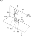
- FIG. 9 is an explanatory diagram schematically depicting an example of a control system using a heatsink HS and a noise eliminator 11 in a circuit diagram related to the power converter 10 according to the embodiment of the present invention.
- Fig. 9 is an explanatory diagram schematically depicting an example of a control system using a heatsink HS and a noise eliminator 11 in a circuit diagram related to the power converter 10 according to the embodiment of the present invention.
- a filter 20 connected to an AC power source (not shown), an AC/DC converter 30 such as a diode bridge which converts alternate current supplied from the AC power source, to the DC current, the power converter 10 which performs power conversion such as smoothing and boosting of a voltage, and an isolation DC/DC converter 40 such as a transformer which performs conversion to a voltage and a current of a specification depending on a power load (not shown).
- the DC current converted from alternate current by the AC/DC converter 30 has a pulsating current in which the minus voltage of the alternate current output from the filter 20 side is reversed, and the DC current converted from alternate current has the same polarity but changes in the magnitude. Then, the power converter 10 smooths the DC voltage supplied as a pulsating current.
- the power converter 10 is provided with a first line 12a and a second line 12b each connecting an input side connected to the AC/DC converter 30 and an output side connected to the isolation DC/DC converter 40.
- the first line 12a and the second line 12b are connected to a first potential and a second potential on the input side.
- the first line 12a is connected to, for example, the plus side as the first potential.
- the second line 12b is connected to, for example, the minus side as the second potential and is used as a line connected to the stable potential lower than the first potential.
- a first capacitor C1 is provided, on the input side which receives an input from the AC/DC converter 30, so as to connect between the first line 12a and the second line 12b. Further, on the output side on which outputting to the isolation DC/DC converter 40 is performed, there are provided a boost circuit using a reactor L, the semiconductor switch SW, a rectifier element D, and a second capacitor C2.
- the reactor L and the rectifier element D provided as the boost circuit are connected in series on the first line 12a.
- the rectifier element D is disposed in a direction in which an anode terminal is on the input side and a cathode terminal is on the output side, and the reactor L is connected in series on the anode side.
- the second capacitor C2 is disposed on the cathode side of the rectifier element D so as to connect between the first line 12a and the second line 12b.
- the semiconductor switch SW of the boost circuit is disposed so as to short-circuit between the first line 12a and the second line 12b.
- a MOSFET using a reverse parallel diode is used as the semiconductor switch SW.
- the drain terminal of the semiconductor switch SW is connected to a first point P1 of the first line 12a which is between the reactor L and the rectifier element D, and the source terminal is connected to a second point P2 of the second line 12b.
- the second point P2 is located between the connection point at which the first capacitor C1 is connected to the second line 12b and the connection point at which the second capacitor C2 is connected to the second line 12b.
- the heatsink HS disposed in the vicinity of the semiconductor switch SW is depicted on the right side of the semiconductor switch SW, and the noise eliminator 11 is disposed between the semiconductor switch SW and the heatsink HS.
- the heatsink HS is connected to the FG (frame ground) at the ground potential.
- the conductive member 11a of the noise eliminator 11 is connected to the second line 12b from the connecting line 11c through the on-board line B1 shown in Fig. 5 and other drawings.
- a first parasitic capacitance Chp1 is generated between the conductive member 11a of the noise eliminator 11 and the semiconductor switch SW, and a second parasitic capacitance Chp2 is generated between the conductive member 11a of the noise eliminator 11 and the heatsink HS.
- the noise current Ins transferred to the second line 12b circulates flowing through the second point P2, the capacitor C1, the reactor L, and the first point P1 and is enclosed in the circuit configured with these elements; therefore, the noise current Ins is not output as noise to the input side of the power converter 10.
- a voltage fluctuation at the second point P2 is transferred from the heatsink HS to the FG, and a common mode current Icm flows as noise.
- Fig. 10 is a graph showing an example of a temporal change in a voltage of the power converter 10.
- the horizontal axis represents time
- the vertical axis represents voltage
- the temporal change of the voltage V2 at the second point P2 is represented by a solid line.
- the temporal change of the voltage V1 at the first point P1 is represented by a broken line.
- Fig. 10 clearly shows that the temporal change of the voltage V2 at the second point P2 is smaller than the temporal change of the voltage V1 at the first point P1.
- the common mode current Icm is smaller. That is, in the case that there is almost no change at the second point P2 connected to the stable potential as exemplified in Fig. 10 , even if the common mode current Icm is output as noise to the input side of the power converter 10, the common mode current Icm is negligibly small.
- the noise eliminator 11 in which the conductive member 11a is covered with the insulator 11b is disposed between the semiconductor switch SW and the heatsink HS, and the conductive member 11a is connected to a line.
- the noise current Ins due to the first parasitic capacitance Chp1 generated between the conductive member 11a of the noise eliminator 11 and the semiconductor switch SW.
- the conductive member 11a is connected to the second line 12b as the stable potential, it is possible to reduce the common mode current Icm due to the second parasitic capacitance Chp2 generated between the conductive member 11a of the noise eliminator 11 and the heatsink HS.
- the noise eliminator 11 even when the conductive member 11a and the insulator 11b constituting the noise eliminator 11 is made thin, noise can be reduced; therefore, there are advantages, for example, that temperature rise can be reduced and that production cost can be reduced. Further, because the heatsink HS can be connected without any problem to the FG so that the heatsink HS is at the same potential as the power converter 10, there are advantages that the distance can be arbitrarily selected without being limited by a standard with respect to an insulation distance, that the components can be highly freely arranged, and that downsizing is possible.
- the conductive member 11a and the insulator 11b can be appropriately designed.
- the shape does not have to be a thin-film shape.
- the shape may be a bulk form having some thickness or a hard flat-plate shape, and in order to improve the thermal conductivity, the shape may be formed to have a surface shape such as a curved surface or concavities and convexities, which are different from a flat plane.
- the insulator 11b may be adhered as an insulating film on each side of the conductive member 11a.
- the present invention is not limited to this form and can be developed into various forms.
- the both ends of a U-shaped engagement member may be fixed on the on-board line B1, and the annular terminal 11d may be freely fit to a ring-shaped engagement member.
- the connecting line 11c can be freely movably engaged with the engagement member, the present invention can be developed into various forms.
- two guide pins may be vertically provided as the engagement member on the circuit board B, and a terminal may be used such that the terminal is held between the guide pins and such that the terminal is guided in the guide pins' direction.
- the above embodiments may be combined in various manners.
- the embodiment can be developed into various combinations.
- the heatsink HS is connected to the FG; however, the heatsink HS can be designed to be connected to a SG (signal ground) or a ground potential such as a ground instead of the FG, or can be designed to be connected to other potentials which can provide a similar effect.
- a SG signal ground
- a ground potential such as a ground instead of the FG
- the power converter 10 according to the present invention is not limited to the above-described embodiments and can be applied, to a technical field such as power electronics, as various devices such as a DC-AC inverter and a DC chopper which use a semiconductor switch.
Description
- The present invention relates to a power converter equipped with a line provided on a circuit board, a switching element provided on the circuit board and connected to the line, and a radiator provided on the circuit board.
- A power converter is used in various applications, in which a semiconductor switch is switched to control an output voltage and/or an output current. To the power converter is attached a heatsink to radiate heat generated by the semiconductor switch.
-
Fig. 1 is a schematic side view schematically showing a semiconductor switch equipped on a power converter and an outer appearance of an attached heatsink.Fig. 1 shows a semiconductor switch SW equipped on the power converter. The semiconductor switch SW is attached with a heatsink HS and is fixed on a circuit board B. The heatsink HS has a function of cooling by externally radiating heat generated on the semiconductor switch SW. - However, when the heatsink HS is connected to an FG (frame ground), a parasitic capacitance is generated between the semiconductor switch SW and the heatsink HS.
-
Fig. 2 is an explanatory diagram schematically depicting the heatsink in a circuit diagram related to the semiconductor switch equipped on the power converter.Fig. 2 shows a circuit in which the semiconductor switch SW is provided to short-circuit between a pair of lines connecting an input side and an output side, and the heatsink HS is shown on the right side of the semiconductor switch SW. The heatsink HS is connected to the FG. Further, a parasitic capacitance Chp is generated between the semiconductor switch SW and the heatsink HS. The generated parasitic capacitance Chp transfers to the FG a voltage fluctuation at a point P1 connected to the positive terminal of the semiconductor switch SW, and whereby a common mode current Icm flows as noise. -
Fig. 3 is a graph showing a voltage change at the point P1 of the power converter.Fig. 3 shows a temporal change of a voltage V1 at the point P1, where the horizontal axis represents time and the vertical axis represents the voltage at the point P1. Because the temporal change of the voltage V1 at the point P1 shown inFig. 3 is transferred to the FG through the parasitic capacitance Chp, the temporal change of the voltage V1 is output as noise to the input side of the power converter. - As described above, when the heatsink HS is connected to the FG, large noise depending on the voltage fluctuation at the point P1 is output to the input side of the power converter. The magnitude of the common mode current Icm to be transferred to the FG and to become noise is represented by the following Equation (A).

- Icm is a common mode current,
- Chp is a parasitic capacitance between the semiconductor switch SW and the heatsink HS,
- V is a voltage V1 at the point P1, and
- t is time.
- The parasitic capacitance Chp is represented by the following Equation (B).

- ε is a permittivity between the semiconductor switch SW and the heatsink HS,
- dhp is a distance between the semiconductor switch SW and the heatsink HS, and
- S is an area of the electrode.
- In order to reduce the above-mentioned noise, Patent Document 1 proposes a method in which a low-permittivity insulation material using ceramics is provided between the semiconductor switch and the heatsink to reduce the parasitic capacitance generated between the semiconductor switch and the heatsink. Because the parasitic capacitance is reduced, the parasitic capacitance Chp in the above Equation (A) is accordingly reduced, and whereby the common mode current Icm can be smaller.
- Further, as another method for reducing the noise, Patent Document 2 proposes a method in which the heatsink itself is connected to a stable potential so that the current causing the noise will be enclosed in a circuit.
-
- Patent Document 1: Japanese Unexamined Patent Publication No.
H9-298889 - Patent Document 2: Japanese Unexamined Patent Publication No.
H11-356047 -
US 2004/0164405 A1 discloses a heatsink arrangement attached to a semiconductor device and including: a first heatsink placed in close contact with the semiconductor device; and a second heatsink placed in close contact with the first heatsink, wherein the first heatsink and the second heatsink are connected to a power supply circuit for the semiconductor device via a first connector and a second connector, respectively. -
US 2001/0272181 A1 discloses a multilayer stretchable cable including a multilayer stretchable film and a plurality of conductive lines in the stretchable film. - However, the method proposed in Patent Document 1 has a problem that the semiconductor switch cannot be sufficiently cooled because of a thermal resistance of the insulation material provided between the semiconductor switch and the heatsink. In addition, there is caused another problem that the ceramics used as the insulation material is expensive so that a cost of the power converter becomes higher.
- Further, in the method proposed in Patent Document 2, when the heatsink is used while being fixed to a casing, it is necessary to provide an insulation distance between a ground potential and the stable potential because the casing is at the ground potential. Therefore, there is caused a problem that a larger space needs to be provided for the heatsink to be disposed in, and this problem leads to another problem such as restriction of arrangement of other elements. Further, the bolt for fixing the heatsink must be made of insulation material. If resin material is used as an insulation material bolt, the strength is not enough, and if ceramics is used, the cost of the power converter becomes higher. On the other hand, if the heatsink is not fixed on the casing, the heatsink needs to be fixed at many positions to ensure fixing strength, and there is a problem such as restriction of arrangement of other elements.
- The present invention has been made in view of these circumstances, and an insertion member having an insulator and a conductive member is provided between the switching element and radiator, where the conductive member and a line on a circuit board are connected to each other by a flexible connecting line. An object of the present invention is to provide a power converter in which the noise can be reduced with the above arrangement without causing the problems described in association with Patent Document 1 and Patent Document 2 and in which an influence of vibration or the like can be reduced and the durability is thus high.
- In order to solve the above problem, a power converter according to the present invention is a power converter according to claim 1. In particular, a power converter includes: a line provided on a circuit board; a switching element provided on the circuit board and connected to the line; a radiator provided on the circuit board; and an insertion member provided between the switching element and the radiator. The insertion member includes: a conductive member; an insulator provided between the conductive member and the switching element and between the conductive member and the radiator; and a connecting line which is flexible and electrically connects the conductive member and the line to each other.
- Further, the power converter includes an engagement member provided on the circuit board and electrically connected to the line, and the connecting line includes a terminal freely movably engaged with the engagement member.
- Further, in the power converter, the engagement member is a pivot support pin one end of which is fixed to the line. The terminal included in the connecting line has a through hole provided therein, and the through hole is freely fit to the pivot support pin.
- Further, in the power converter, the connecting line includes a bellows member formed in a bellows shape.
- Further, in the power converter, the connecting line includes a helical member formed in a helical shape.
- Further, in the power converter, the line is a pair of lines connecting between an input side and an output side, the switching element is provided to short-circuit between the pair of lines, one of the pair of lines is connected to a stable potential, the connecting line electrically connects the conductive member to the one of the pair of lines connected to the stable potential, and the radiator is electrically connected to a predetermined potential.
- In the power converter according to the present invention, noise caused by a parasitic capacitance can be enclosed in a circuit, and the flexibility of a connecting line reduces an influence of vibration or the like.
- In the present invention, an insertion member having an insulator and a conductive member is provided between a switching element and a radiator, and the conductive member and a line on a circuit board are connected to each other by a flexible connecting line. This arrangement enables a noise current to flow to the line side, the noise current being based on parasitic capacitances generated between the conductive member and the switching element and between the conductive member and the radiator. Therefore, the noise is enclosed in a circuit, and an excellent effect is provided. For example, the noise which is output to the input side of the power converter can be reduced. In addition, because the connecting line connecting the conductive member and the line is flexible, an excellent effect is provided. For example, it is possible to reduce the influence of a physical stimulation such as vibration.
-
-
Fig. 1 is a schematic side view schematically showing an outer appearance of a semiconductor switch equipped on a power converter and an attached heatsink; -
Fig. 2 is an explanatory diagram schematically depicting the heatsink on a circuit diagram related to the semiconductor switch equipped on the power converter; -
Fig. 3 is a graph showing a voltage change at a point in the power converter; -
Fig. 4 is a schematic side view schematically showing an example of an outer appearance of a power converter according to an embodiment of the present invention; -
Fig. 5 is a schematic perspective view schematically showing an example of an outer appearance of the power converter according to the embodiment of the present invention; -
Fig. 6 is a schematic diagram schematically showing an example of a noise eliminator and a pivot support pin equipped on the power converter according to the embodiment of the present invention; -
Fig. 7A is a schematic diagram schematically showing another example of the noise eliminator equipped on the power converter of the embodiment of the present invention; -
Fig. 7B is a schematic diagram schematically showing another example of the noise eliminator equipped on the power converter of the embodiment of the present invention; -
Fig. 7C is a schematic diagram schematically showing another example of the noise eliminator equipped on the power converter of the embodiment of the present invention; -
Fig. 8 is a schematic diagram schematically showing another example of the noise eliminator equipped on the power converter of the embodiment of the present invention; -
Fig. 9 is an explanatory diagram schematically depicting an example of a control system using a heatsink and a noise eliminator in a circuit diagram related to the power converter according to the embodiment of the present invention; and -
Fig. 10 is a graph showing an example of a temporal change in a voltage of a power converter. - Hereinafter, an embodiment of the present invention will be described with reference to the drawings. Note that the following embodiment is an example in which the present invention is embodied, and the embodiment is not intended to limit the technical scope of the present invention.
-
Fig. 4 is a schematic side view schematically showing an example of an outer appearance of a power converter according to the embodiment of the present invention.Fig. 5 is a schematic perspective view schematically showing an example of an outer appearance of the power converter according to the embodiment of the present invention.Fig. 6 is a schematic diagram schematically showing an example of a noise eliminator and a pivot support pin equipped on the power converter according to the embodiment of the present invention. Apower converter 10 according to the present invention is a device such as an inverter or a DC/DC converter in which a semiconductor switch SW is used to perform control of conversion of an output voltage and/or an output current. - The semiconductor switch SW is configured with a semiconductor switching element such as a MOSFET (Metal-Oxide-Semiconductor Field-Effect Transistor) or an IGBT (Insulated Gate Bipolar Transistor). The semiconductor switch SW is fixed on a circuit board B by using a source terminal Ssw, a gate terminal Gsw, and a drain terminal Dsw which function as legs. Further, on the circuit board B is vertically provided a heatsink (radiator) HS which has a function of cooling by externally radiating heat generated on the semiconductor switch SW. The heatsink HS is approximately perpendicular to the upper surface of the circuit board B, and the heatsink HS is electrically connected to an FG (frame ground) to be described later. Further, on the circuit board B, a noise eliminator (insertion member) 11 is provided between the semiconductor switch SW and the heatsink HS, and the
noise eliminator 11 reduces a noise current flowing, from a parasitic capacitance generated between the semiconductor switch SW and the heatsink HS, to the input side of thepower converter 10. - The
noise eliminator 11 is equipped with a thin-film shapedconductive member 11a such as a copper foil, aninsulator 11b covering theconductive member 11a, and a connectingline 11c connected to theconductive member 11a. Theconductive member 11a is electrically connected to an on-board line B1 provided on the circuit board B, through the flexible connectingline 11c. Thenoise eliminator 11 has a thin-film shape in which the thin-film shapedconductive member 11a is covered with the thin-film shaped insulator (insulating film) 11b, and one surface of theinsulator 11b is adhered to the semiconductor switch SW, and the other surface is adhered to the heatsink HS. Specifically, theconductive member 11a is disposed between the semiconductor switch SW and the heatsink HS, and theinsulator 11b is disposed, as an insulating film, between theconductive member 11a and the semiconductor switch SW and between theconductive member 11a and the heatsink HS. Further, in order to increase an efficiency of heat transfer at which the heat generated on the semiconductor switch SW is transferred to the heatsink HS through thenoise eliminator 11, the semiconductor switch SW has a heat radiation surface to be adhered to one surface of thenoise eliminator 11, and the heatsink HS has a heat absorption surface to be adhered to the other surface of thenoise eliminator 11. - On one end side of the on-board line B1 provided on the circuit board B is fixed the source terminal Ssw, and on a line terminal B2 on the other end side is fixed a conductive pivot support pin B3 as an engagement member. The pivot support pin B3 has a rod shape and is vertically disposed to be approximately perpendicular to the upper surface of the circuit board B while one end of the pivot support pin B3 is fixed on the line terminal B2. Further, the end of the connecting
line 11c extending from theconductive member 11a of thenoise eliminator 11 is formed to be a conductiveannular terminal 11d in which a through hole is made, and theannular terminal 11d is freely fit to the pivot support pin B3 via the through hole and is freely movably engaged with the pivot support pin B3. Because theannular terminal 11d is engaged with the pivot support pin B3, theconductive member 11a of thenoise eliminator 11 is electrically connected to the on-board line B1 and the source terminal Ssw. - The connecting
line 11c is made up of a thin film having an elongated shape and is made longer than the distance between the connection position of the connectingline 11c to theconductive member 11a and the on-board line B1. Therefore, even when a physical vibration occurs in a direction of the hollow arrows inFig. 5 , the longish part of the connectingline 11c absorbs the vibration by the flexibility, and whereby it is possible to reduce occurrence of abnormality such as fracture at the connection part or break caused by physical stimulation such as vibration. In particular, in the form exemplified inFig. 5 , because theannular terminal 11d is freely movably engaged with the pivot support pin B3, physical stimulation such as vibration can be absorbed also by the free movement of theannular terminal 11d, and whereby occurrence of abnormality can be effectively reduced. - The flexible connecting
line 11c exemplified inFig. 4 to Fig. 6 can be formed in various shapes.Fig. 7A to Fig. 7C are schematic diagrams each schematically showing another example of thenoise eliminator 11 equipped on thepower converter 10 according to the embodiment of the present invention.Fig. 7A shows a form in which the connectingline 11c using a thin film having an elongated shape is made in a bellows shape. With respect to physical stimulation such as vibration, the connectingline 11c made in a bellows shape can absorb the vibration by the bellows member expanding and contracting while bending. -
Fig. 7B shows a form in which the connectingline 11c using a thin film having an elongated shape is made in a helical shape. With respect to physical stimulation such as vibration, the connectingline 11c made in a helical shape can absorb the vibration by the helical member expanding and contracting as a spring. -
Fig. 7C shows a form in which the connectingline 11c is made of a threadlike conductive member.Fig. 7C shows a form in which a threadlike conductive member (for example, an elongated copper wire) is used in a slack manner, and the threadlike conductive member is sufficiently longer than the distance between the connection position of the connectingline 11c to theconductive member 11a and the on-board line B1. In the connectingline 11c using a sufficiently long threadlike conductive member, the slack part can absorb physical stimulation such as vibration, so that the vibration can be prevented from being transferred. -
Fig. 8 is a schematic diagram schematically showing another example of thenoise eliminator 11 equipped on thepower converter 10 according to the embodiment of the present invention. Thenoise eliminator 11 exemplified inFig. 8 has a form in which the end of the connectingline 11c is directly fixed on the line terminal B2 without using a pivot support pin B3. Even in the case that the end of the connectingline 11c is directly fixed on the line terminal B2 without using a pivot support pin B3, if the connectingline 11c is sufficiently long and flexible, it is possible to absorb vibration of physical stimulation such as vibration. - Next, an embodiment of a circuit configuration of the
power converter 10 in the above-mentioned configuration will be described.Fig. 9 is an explanatory diagram schematically depicting an example of a control system using a heatsink HS and anoise eliminator 11 in a circuit diagram related to thepower converter 10 according to the embodiment of the present invention. In the form exemplified inFig. 9 , there are used afilter 20 connected to an AC power source (not shown), an AC/DC converter 30 such as a diode bridge which converts alternate current supplied from the AC power source, to the DC current, thepower converter 10 which performs power conversion such as smoothing and boosting of a voltage, and an isolation DC/DC converter 40 such as a transformer which performs conversion to a voltage and a current of a specification depending on a power load (not shown). The DC current converted from alternate current by the AC/DC converter 30 has a pulsating current in which the minus voltage of the alternate current output from thefilter 20 side is reversed, and the DC current converted from alternate current has the same polarity but changes in the magnitude. Then, thepower converter 10 smooths the DC voltage supplied as a pulsating current. - The
power converter 10 is provided with afirst line 12a and asecond line 12b each connecting an input side connected to the AC/DC converter 30 and an output side connected to the isolation DC/DC converter 40. Thefirst line 12a and thesecond line 12b are connected to a first potential and a second potential on the input side. Thefirst line 12a is connected to, for example, the plus side as the first potential. Thesecond line 12b is connected to, for example, the minus side as the second potential and is used as a line connected to the stable potential lower than the first potential. - In the
power converter 10, a first capacitor C1 is provided, on the input side which receives an input from the AC/DC converter 30, so as to connect between thefirst line 12a and thesecond line 12b. Further, on the output side on which outputting to the isolation DC/DC converter 40 is performed, there are provided a boost circuit using a reactor L, the semiconductor switch SW, a rectifier element D, and a second capacitor C2. - The reactor L and the rectifier element D provided as the boost circuit are connected in series on the
first line 12a. The rectifier element D is disposed in a direction in which an anode terminal is on the input side and a cathode terminal is on the output side, and the reactor L is connected in series on the anode side. Further, the second capacitor C2 is disposed on the cathode side of the rectifier element D so as to connect between thefirst line 12a and thesecond line 12b. - Further, the semiconductor switch SW of the boost circuit is disposed so as to short-circuit between the
first line 12a and thesecond line 12b. For a circuit exemplified inFig. 5 , a MOSFET using a reverse parallel diode is used as the semiconductor switch SW. The drain terminal of the semiconductor switch SW is connected to a first point P1 of thefirst line 12a which is between the reactor L and the rectifier element D, and the source terminal is connected to a second point P2 of thesecond line 12b. Note that the second point P2 is located between the connection point at which the first capacitor C1 is connected to thesecond line 12b and the connection point at which the second capacitor C2 is connected to thesecond line 12b. - In
Fig. 9 , the heatsink HS disposed in the vicinity of the semiconductor switch SW is depicted on the right side of the semiconductor switch SW, and thenoise eliminator 11 is disposed between the semiconductor switch SW and the heatsink HS. The heatsink HS is connected to the FG (frame ground) at the ground potential. Theconductive member 11a of thenoise eliminator 11 is connected to thesecond line 12b from the connectingline 11c through the on-board line B1 shown inFig. 5 and other drawings. - In addition to the above-described various types of elements, a first parasitic capacitance Chp1 is generated between the
conductive member 11a of thenoise eliminator 11 and the semiconductor switch SW, and a second parasitic capacitance Chp2 is generated between theconductive member 11a of thenoise eliminator 11 and the heatsink HS. - Through the first parasitic capacitance Chp1 generated between the
conductive member 11a of thenoise eliminator 11 and the semiconductor switch SW, a voltage fluctuation at the first point P1 is transferred from theconductive member 11a to thesecond line 12b through the second point P2, and a noise current Ins flows. However, the noise current Ins transferred to thesecond line 12b circulates flowing through the second point P2, the capacitor C1, the reactor L, and the first point P1 and is enclosed in the circuit configured with these elements; therefore, the noise current Ins is not output as noise to the input side of thepower converter 10. - Further, through the second parasitic capacitance Chp2 generated between the
conductive member 11a of thenoise eliminator 11 and the heatsink HS, a voltage fluctuation at the second point P2 is transferred from the heatsink HS to the FG, and a common mode current Icm flows as noise. In this case, a magnitude of the flowing common mode current Icm can be represented by the following Equation (1).
- Icm is the common mode current,
- Chp2 is the parasitic capacitance between the
conductive member 11a and the heatsink HS, - V is the voltage V2 at the second point P2, and
- t is time.
- The voltage at the second point P2 shown in Equation (1) will be described.
Fig. 10 is a graph showing an example of a temporal change in a voltage of thepower converter 10. InFig. 10 , the horizontal axis represents time, the vertical axis represents voltage, and the temporal change of the voltage V2 at the second point P2 is represented by a solid line. Further, for the purpose of comparison, the temporal change of the voltage V1 at the first point P1 is represented by a broken line.Fig. 10 clearly shows that the temporal change of the voltage V2 at the second point P2 is smaller than the temporal change of the voltage V1 at the first point P1. Therefore, because the value of dV/dt in Equation (1) caused by the temporal change at the second point P2 is smaller than the value caused by the temporal change at the first point P1, the common mode current Icm is smaller. That is, in the case that there is almost no change at the second point P2 connected to the stable potential as exemplified inFig. 10 , even if the common mode current Icm is output as noise to the input side of thepower converter 10, the common mode current Icm is negligibly small. - As described above, in the
power converter 10 described in the present application, thenoise eliminator 11 in which theconductive member 11a is covered with theinsulator 11b is disposed between the semiconductor switch SW and the heatsink HS, and theconductive member 11a is connected to a line. With this arrangement, it is possible to enclose in thepower converter 10 the noise current Ins due to the first parasitic capacitance Chp1 generated between theconductive member 11a of thenoise eliminator 11 and the semiconductor switch SW. Further, when theconductive member 11a is connected to thesecond line 12b as the stable potential, it is possible to reduce the common mode current Icm due to the second parasitic capacitance Chp2 generated between theconductive member 11a of thenoise eliminator 11 and the heatsink HS. In addition, even when theconductive member 11a and theinsulator 11b constituting thenoise eliminator 11 is made thin, noise can be reduced; therefore, there are advantages, for example, that temperature rise can be reduced and that production cost can be reduced. Further, because the heatsink HS can be connected without any problem to the FG so that the heatsink HS is at the same potential as thepower converter 10, there are advantages that the distance can be arbitrarily selected without being limited by a standard with respect to an insulation distance, that the components can be highly freely arranged, and that downsizing is possible. - The present invention is not limited to the above-described embodiment and can be carried out in various forms. Therefore, the above-mentioned embodiment is just an example at any points and should not be restrictively interpreted. The scope of the present invention is defined by the accompanying claims and is not limited to the main body of the specification at all. Further, deformations and variations within the scope of the equivalents of the claims are all within the scope of the present invention.
- For example, as long as the
conductive member 11a is disposed between the semiconductor switch SW and the heatsink HS and theinsulator 11b is disposed as an insulating film between theconductive member 11a and the semiconductor switch SW and between theconductive member 11a and the heatsink HS, theconductive member 11a and theinsulator 11b can be appropriately designed. For example, the shape does not have to be a thin-film shape. The shape may be a bulk form having some thickness or a hard flat-plate shape, and in order to improve the thermal conductivity, the shape may be formed to have a surface shape such as a curved surface or concavities and convexities, which are different from a flat plane. Further, instead of covering theconductive member 11a with theinsulator 11b, theinsulator 11b may be adhered as an insulating film on each side of theconductive member 11a. - In the form described in the above embodiment, only one end of the pivot support pin B3 is fixed on the on-board line B1; however, the present invention is not limited to this form and can be developed into various forms. For example, the both ends of a U-shaped engagement member may be fixed on the on-board line B1, and the
annular terminal 11d may be freely fit to a ring-shaped engagement member. Further, if the connectingline 11c can be freely movably engaged with the engagement member, the present invention can be developed into various forms. For example, two guide pins may be vertically provided as the engagement member on the circuit board B, and a terminal may be used such that the terminal is held between the guide pins and such that the terminal is guided in the guide pins' direction. - Further, the above embodiments may be combined in various manners. For example, the embodiment can be developed into various combinations. For example, it is possible to use a connecting
line 11c having a bellows-shaped bellows member and a helical-shaped helical member. - In the form described in the above embodiment, the heatsink HS is connected to the FG; however, the heatsink HS can be designed to be connected to a SG (signal ground) or a ground potential such as a ground instead of the FG, or can be designed to be connected to other potentials which can provide a similar effect.
- Further, the
power converter 10 according to the present invention is not limited to the above-described embodiments and can be applied, to a technical field such as power electronics, as various devices such as a DC-AC inverter and a DC chopper which use a semiconductor switch. -
- 10
- power converter
- 11
- noise eliminator
- 11a
- conductive member
- 11b
- insulator (insulating film)
- 11c
- connecting line
- 11d
- annular terminal
- 12a
- first line
- 12b
- second line
- B
- circuit board
- B1
- on-board line
- B2
- line terminal
- B3
- pivot support pin (engagement member)
- Chp1
- first parasitic capacitance
- Chp2
- second parasitic capacitance
- HS
- heatsink (radiator)
- SW
- semiconductor switch
Claims (6)
- A power converter (10) comprising:a line (12a, 12b) provided on a circuit board (B);a switching element (SW) provided on the circuit board (B) and connected to the line (12a, 12b, B1);a radiator (HS) provided on the circuit board (B) perpendicular to an upper surface of the circuit board (B); andan insertion member (11) provided between the switching element (SW) and the radiator (HS), wherein a heat radiation surface of the switching element (SW) is adhered to one surface of the insertion member (11), and a heat absorption surface of the radiator (HS) is adhered to the other surface of the insertion member (11), the insertion member (11) including:a conductive member (11a);an insulator (11b) provided between the conductive member (11a) and the switching element (SW) and between the conductive member (11a) and the radiator (HS); anda connecting line (11c) which is flexible and electrically connects the conductive member (11a) and the line to each other,
characterized in thatan on-board line (B1) is provided on the circuit board (B), one end side of the on-board line (B1) is fixed to a terminal of the switching element (SW) connected to the line (12a, 12b) and the other end side of the on-board line (B1) is a line terminal (B2) connected to the connecting line (11c), andthe flexible connecting line (11c) is made longer than a distance between a connection position of the connecting line (11c) to the conductive member (11a) and a connection position of the connecting line (11c) to the on-board line (B1). - The power converter according to claim 1, comprising:an engagement member (B3) provided on the circuit board (B) and electrically connected to the line (12a, 12b),wherein the connecting line (11c) includes a terminal (11d) freely movably engaged with the engagement member (B3).
- The power converter according to claim 2, wherein the engagement member (B3) is a pivot support pin one end of which is fixed to the line (12a, 12b), and
the terminal (11d) included in the connecting line (11c) includes a through hole provided therein, the through hole being freely fit to the pivot support pin (B3). - The power converter according to any one of claims 1 to 3, wherein the connecting line (11c) includes a bellows member formed in a bellows shape.
- The power converter according to any one of claims 1 to 4, wherein the connecting line (11c) includes a helical member formed in a helical shape.
- The power converter according to any one of claims 1 to 5, wherein the line is a pair of lines (12a, 12b) connecting between an input side and an output side of the power converter (10),
the switching element (SW) is provided to short-circuit between the pair of lines (12a, 12b),
one of the pair of lines (12b) is connected to a stable potential,
the connecting line (11c) electrically connects the conductive member (11a) to the one of the pair of lines (12b) connected to the stable potential, and
the radiator (HS) is electrically connected to a predetermined potential.
Applications Claiming Priority (2)
| Application Number | Priority Date | Filing Date | Title |
|---|---|---|---|
| JP2015131439A JP6447391B2 (en) | 2015-06-30 | 2015-06-30 | Power converter |
| PCT/JP2016/057180 WO2017002399A1 (en) | 2015-06-30 | 2016-03-08 | Power conversion device |
Publications (3)
| Publication Number | Publication Date |
|---|---|
| EP3276807A1 EP3276807A1 (en) | 2018-01-31 |
| EP3276807A4 EP3276807A4 (en) | 2018-06-13 |
| EP3276807B1 true EP3276807B1 (en) | 2019-11-20 |
Family
ID=57608090
Family Applications (1)
| Application Number | Title | Priority Date | Filing Date |
|---|---|---|---|
| EP16817509.9A Active EP3276807B1 (en) | 2015-06-30 | 2016-03-08 | Power conversion device |
Country Status (5)
| Country | Link |
|---|---|
| US (1) | US10244617B2 (en) |
| EP (1) | EP3276807B1 (en) |
| JP (1) | JP6447391B2 (en) |
| CN (1) | CN107636945B (en) |
| WO (1) | WO2017002399A1 (en) |
Families Citing this family (2)
| Publication number | Priority date | Publication date | Assignee | Title |
|---|---|---|---|---|
| JP6511992B2 (en) * | 2015-06-30 | 2019-05-15 | オムロン株式会社 | Power converter |
| JP2024015805A (en) * | 2022-07-25 | 2024-02-06 | マツダ株式会社 | Switching devices and switching modules |
Family Cites Families (14)
| Publication number | Priority date | Publication date | Assignee | Title |
|---|---|---|---|---|
| US5459348A (en) * | 1991-05-24 | 1995-10-17 | Astec International, Ltd. | Heat sink and electromagnetic interference shield assembly |
| JP2973799B2 (en) * | 1993-04-23 | 1999-11-08 | 富士電機株式会社 | Power transistor module |
| JP3649259B2 (en) | 1996-04-26 | 2005-05-18 | 株式会社安川電機 | Inverter device |
| JPH11356047A (en) | 1998-06-08 | 1999-12-24 | Cosel Co Ltd | Switching regulator |
| JP3858834B2 (en) * | 2003-02-24 | 2006-12-20 | オンキヨー株式会社 | Semiconductor element heatsink |
| JP2007213690A (en) * | 2006-02-09 | 2007-08-23 | Funai Electric Co Ltd | Dvd player |
| US8242375B2 (en) * | 2008-09-18 | 2012-08-14 | United Technologies Corporation | Conductive emissions protection |
| JP5240215B2 (en) * | 2010-02-17 | 2013-07-17 | 日立電線株式会社 | Circuit board and power conversion device using the same |
| KR101130697B1 (en) * | 2010-05-07 | 2012-04-02 | 삼성전자주식회사 | Multilayer stretchable cable |
| JP5675526B2 (en) * | 2011-08-02 | 2015-02-25 | トヨタ自動車株式会社 | Power converter |
| JP5591211B2 (en) * | 2011-11-17 | 2014-09-17 | 三菱電機株式会社 | Power converter |
| JP5987163B2 (en) * | 2012-09-07 | 2016-09-07 | パナソニックIpマネジメント株式会社 | Power converter |
| KR20160135800A (en) * | 2014-03-21 | 2016-11-28 | 로베르트 보쉬 게엠베하 | Common mode noise suppression of switch-mode power converters by capacitive shield with damping network |
| DE112015000245T5 (en) * | 2014-07-30 | 2016-09-15 | Fuji Electric Co., Ltd. | Semiconductor module |
-
2015
- 2015-06-30 JP JP2015131439A patent/JP6447391B2/en active Active
-
2016
- 2016-03-08 WO PCT/JP2016/057180 patent/WO2017002399A1/en active Application Filing
- 2016-03-08 CN CN201680022858.5A patent/CN107636945B/en active Active
- 2016-03-08 EP EP16817509.9A patent/EP3276807B1/en active Active
-
2017
- 2017-10-17 US US15/785,563 patent/US10244617B2/en active Active
Non-Patent Citations (1)
| Title |
|---|
| None * |
Also Published As
| Publication number | Publication date |
|---|---|
| JP2017017841A (en) | 2017-01-19 |
| EP3276807A4 (en) | 2018-06-13 |
| US20180042104A1 (en) | 2018-02-08 |
| US10244617B2 (en) | 2019-03-26 |
| WO2017002399A1 (en) | 2017-01-05 |
| CN107636945B (en) | 2019-09-06 |
| EP3276807A1 (en) | 2018-01-31 |
| JP6447391B2 (en) | 2019-01-09 |
| CN107636945A (en) | 2018-01-26 |
Similar Documents
| Publication | Publication Date | Title |
|---|---|---|
| JP6827085B2 (en) | High voltage power module | |
| US10177676B2 (en) | Power converter | |
| JP4775475B2 (en) | Power converter | |
| WO2018129961A1 (en) | Magnetic coupling resonant power emission end having multiple resonant circuits connected in parallel, receiving end, and system | |
| US10134718B2 (en) | Power semiconductor module | |
| EP2928057A1 (en) | Power converting device and railway vehicle mounted with the same | |
| EP3276807B1 (en) | Power conversion device | |
| JP6158051B2 (en) | Power converter | |
| US10361628B2 (en) | Power converter | |
| JP2009027778A (en) | Bus bar | |
| CN109429543B (en) | Power conversion device | |
| JP6102668B2 (en) | Power converter | |
| CN112514224A (en) | High-voltage filter and power conversion device | |
| US20170280595A1 (en) | Electronic device | |
| US7655982B2 (en) | Output control device, and AC/DC power source device, circuit device, LED backlight circuit device, and switching DC/DC converter device each using output control device | |
| CN103930986A (en) | Power conversion apparatus | |
| CN104066311B (en) | Substrate gap retaining member and DC-to-AC converter | |
| JP5040418B2 (en) | Semiconductor device | |
| EP3376658B1 (en) | Power conversion device and power supply apparatus | |
| US20240128885A1 (en) | Power converter | |
| JP6608252B2 (en) | Power semiconductor module and power conversion device | |
| WO2019053942A1 (en) | Semiconductor module |
Legal Events
| Date | Code | Title | Description |
|---|---|---|---|
| STAA | Information on the status of an ep patent application or granted ep patent |
Free format text: STATUS: THE INTERNATIONAL PUBLICATION HAS BEEN MADE |
|
| PUAI | Public reference made under article 153(3) epc to a published international application that has entered the european phase |
Free format text: ORIGINAL CODE: 0009012 |
|
| STAA | Information on the status of an ep patent application or granted ep patent |
Free format text: STATUS: REQUEST FOR EXAMINATION WAS MADE |
|
| 17P | Request for examination filed |
Effective date: 20171023 |
|
| AK | Designated contracting states |
Kind code of ref document: A1 Designated state(s): AL AT BE BG CH CY CZ DE DK EE ES FI FR GB GR HR HU IE IS IT LI LT LU LV MC MK MT NL NO PL PT RO RS SE SI SK SM TR |
|
| AX | Request for extension of the european patent |
Extension state: BA ME |
|
| REG | Reference to a national code |
Ref country code: DE Ref legal event code: R079 Ref document number: 602016024824 Country of ref document: DE Free format text: PREVIOUS MAIN CLASS: H02M0003155000 Ipc: H02M0001440000 |
|
| A4 | Supplementary search report drawn up and despatched |
Effective date: 20180514 |
|
| RIC1 | Information provided on ipc code assigned before grant |
Ipc: H02M 1/44 20070101AFI20180508BHEP Ipc: H05K 1/02 20060101ALI20180508BHEP Ipc: H01L 23/36 20060101ALI20180508BHEP Ipc: H01R 13/6466 20110101ALI20180508BHEP Ipc: H01L 23/522 20060101ALI20180508BHEP |
|
| DAV | Request for validation of the european patent (deleted) | ||
| DAX | Request for extension of the european patent (deleted) | ||
| GRAP | Despatch of communication of intention to grant a patent |
Free format text: ORIGINAL CODE: EPIDOSNIGR1 |
|
| STAA | Information on the status of an ep patent application or granted ep patent |
Free format text: STATUS: GRANT OF PATENT IS INTENDED |
|
| INTG | Intention to grant announced |
Effective date: 20190527 |
|
| GRAJ | Information related to disapproval of communication of intention to grant by the applicant or resumption of examination proceedings by the epo deleted |
Free format text: ORIGINAL CODE: EPIDOSDIGR1 |
|
| STAA | Information on the status of an ep patent application or granted ep patent |
Free format text: STATUS: REQUEST FOR EXAMINATION WAS MADE |
|
| GRAR | Information related to intention to grant a patent recorded |
Free format text: ORIGINAL CODE: EPIDOSNIGR71 |
|
| GRAS | Grant fee paid |
Free format text: ORIGINAL CODE: EPIDOSNIGR3 |
|
| STAA | Information on the status of an ep patent application or granted ep patent |
Free format text: STATUS: GRANT OF PATENT IS INTENDED |
|
| GRAA | (expected) grant |
Free format text: ORIGINAL CODE: 0009210 |
|
| STAA | Information on the status of an ep patent application or granted ep patent |
Free format text: STATUS: THE PATENT HAS BEEN GRANTED |
|
| INTC | Intention to grant announced (deleted) | ||
| INTG | Intention to grant announced |
Effective date: 20191009 |
|
| AK | Designated contracting states |
Kind code of ref document: B1 Designated state(s): AL AT BE BG CH CY CZ DE DK EE ES FI FR GB GR HR HU IE IS IT LI LT LU LV MC MK MT NL NO PL PT RO RS SE SI SK SM TR |
|
| REG | Reference to a national code |
Ref country code: GB Ref legal event code: FG4D |
|
| REG | Reference to a national code |
Ref country code: CH Ref legal event code: EP |
|
| REG | Reference to a national code |
Ref country code: DE Ref legal event code: R096 Ref document number: 602016024824 Country of ref document: DE |
|
| REG | Reference to a national code |
Ref country code: IE Ref legal event code: FG4D |
|
| REG | Reference to a national code |
Ref country code: AT Ref legal event code: REF Ref document number: 1205327 Country of ref document: AT Kind code of ref document: T Effective date: 20191215 |
|
| REG | Reference to a national code |
Ref country code: NL Ref legal event code: MP Effective date: 20191120 |
|
| REG | Reference to a national code |
Ref country code: LT Ref legal event code: MG4D |
|
| PG25 | Lapsed in a contracting state [announced via postgrant information from national office to epo] |
Ref country code: GR Free format text: LAPSE BECAUSE OF FAILURE TO SUBMIT A TRANSLATION OF THE DESCRIPTION OR TO PAY THE FEE WITHIN THE PRESCRIBED TIME-LIMIT Effective date: 20200221 Ref country code: NO Free format text: LAPSE BECAUSE OF FAILURE TO SUBMIT A TRANSLATION OF THE DESCRIPTION OR TO PAY THE FEE WITHIN THE PRESCRIBED TIME-LIMIT Effective date: 20200220 Ref country code: FI Free format text: LAPSE BECAUSE OF FAILURE TO SUBMIT A TRANSLATION OF THE DESCRIPTION OR TO PAY THE FEE WITHIN THE PRESCRIBED TIME-LIMIT Effective date: 20191120 Ref country code: LT Free format text: LAPSE BECAUSE OF FAILURE TO SUBMIT A TRANSLATION OF THE DESCRIPTION OR TO PAY THE FEE WITHIN THE PRESCRIBED TIME-LIMIT Effective date: 20191120 Ref country code: BG Free format text: LAPSE BECAUSE OF FAILURE TO SUBMIT A TRANSLATION OF THE DESCRIPTION OR TO PAY THE FEE WITHIN THE PRESCRIBED TIME-LIMIT Effective date: 20200220 Ref country code: NL Free format text: LAPSE BECAUSE OF FAILURE TO SUBMIT A TRANSLATION OF THE DESCRIPTION OR TO PAY THE FEE WITHIN THE PRESCRIBED TIME-LIMIT Effective date: 20191120 Ref country code: SE Free format text: LAPSE BECAUSE OF FAILURE TO SUBMIT A TRANSLATION OF THE DESCRIPTION OR TO PAY THE FEE WITHIN THE PRESCRIBED TIME-LIMIT Effective date: 20191120 Ref country code: LV Free format text: LAPSE BECAUSE OF FAILURE TO SUBMIT A TRANSLATION OF THE DESCRIPTION OR TO PAY THE FEE WITHIN THE PRESCRIBED TIME-LIMIT Effective date: 20191120 |
|
| PG25 | Lapsed in a contracting state [announced via postgrant information from national office to epo] |
Ref country code: RS Free format text: LAPSE BECAUSE OF FAILURE TO SUBMIT A TRANSLATION OF THE DESCRIPTION OR TO PAY THE FEE WITHIN THE PRESCRIBED TIME-LIMIT Effective date: 20191120 Ref country code: HR Free format text: LAPSE BECAUSE OF FAILURE TO SUBMIT A TRANSLATION OF THE DESCRIPTION OR TO PAY THE FEE WITHIN THE PRESCRIBED TIME-LIMIT Effective date: 20191120 Ref country code: IS Free format text: LAPSE BECAUSE OF FAILURE TO SUBMIT A TRANSLATION OF THE DESCRIPTION OR TO PAY THE FEE WITHIN THE PRESCRIBED TIME-LIMIT Effective date: 20200320 |
|
| PG25 | Lapsed in a contracting state [announced via postgrant information from national office to epo] |
Ref country code: AL Free format text: LAPSE BECAUSE OF FAILURE TO SUBMIT A TRANSLATION OF THE DESCRIPTION OR TO PAY THE FEE WITHIN THE PRESCRIBED TIME-LIMIT Effective date: 20191120 |
|
| PG25 | Lapsed in a contracting state [announced via postgrant information from national office to epo] |
Ref country code: PT Free format text: LAPSE BECAUSE OF FAILURE TO SUBMIT A TRANSLATION OF THE DESCRIPTION OR TO PAY THE FEE WITHIN THE PRESCRIBED TIME-LIMIT Effective date: 20200412 Ref country code: EE Free format text: LAPSE BECAUSE OF FAILURE TO SUBMIT A TRANSLATION OF THE DESCRIPTION OR TO PAY THE FEE WITHIN THE PRESCRIBED TIME-LIMIT Effective date: 20191120 Ref country code: RO Free format text: LAPSE BECAUSE OF FAILURE TO SUBMIT A TRANSLATION OF THE DESCRIPTION OR TO PAY THE FEE WITHIN THE PRESCRIBED TIME-LIMIT Effective date: 20191120 Ref country code: CZ Free format text: LAPSE BECAUSE OF FAILURE TO SUBMIT A TRANSLATION OF THE DESCRIPTION OR TO PAY THE FEE WITHIN THE PRESCRIBED TIME-LIMIT Effective date: 20191120 Ref country code: ES Free format text: LAPSE BECAUSE OF FAILURE TO SUBMIT A TRANSLATION OF THE DESCRIPTION OR TO PAY THE FEE WITHIN THE PRESCRIBED TIME-LIMIT Effective date: 20191120 Ref country code: DK Free format text: LAPSE BECAUSE OF FAILURE TO SUBMIT A TRANSLATION OF THE DESCRIPTION OR TO PAY THE FEE WITHIN THE PRESCRIBED TIME-LIMIT Effective date: 20191120 |
|
| REG | Reference to a national code |
Ref country code: AT Ref legal event code: MK05 Ref document number: 1205327 Country of ref document: AT Kind code of ref document: T Effective date: 20191120 |
|
| REG | Reference to a national code |
Ref country code: DE Ref legal event code: R097 Ref document number: 602016024824 Country of ref document: DE |
|
| PG25 | Lapsed in a contracting state [announced via postgrant information from national office to epo] |
Ref country code: SM Free format text: LAPSE BECAUSE OF FAILURE TO SUBMIT A TRANSLATION OF THE DESCRIPTION OR TO PAY THE FEE WITHIN THE PRESCRIBED TIME-LIMIT Effective date: 20191120 Ref country code: SK Free format text: LAPSE BECAUSE OF FAILURE TO SUBMIT A TRANSLATION OF THE DESCRIPTION OR TO PAY THE FEE WITHIN THE PRESCRIBED TIME-LIMIT Effective date: 20191120 |
|
| PLBE | No opposition filed within time limit |
Free format text: ORIGINAL CODE: 0009261 |
|
| STAA | Information on the status of an ep patent application or granted ep patent |
Free format text: STATUS: NO OPPOSITION FILED WITHIN TIME LIMIT |
|
| 26N | No opposition filed |
Effective date: 20200821 |
|
| PG25 | Lapsed in a contracting state [announced via postgrant information from national office to epo] |
Ref country code: MC Free format text: LAPSE BECAUSE OF FAILURE TO SUBMIT A TRANSLATION OF THE DESCRIPTION OR TO PAY THE FEE WITHIN THE PRESCRIBED TIME-LIMIT Effective date: 20191120 |
|
| REG | Reference to a national code |
Ref country code: CH Ref legal event code: PL |
|
| PG25 | Lapsed in a contracting state [announced via postgrant information from national office to epo] |
Ref country code: SI Free format text: LAPSE BECAUSE OF FAILURE TO SUBMIT A TRANSLATION OF THE DESCRIPTION OR TO PAY THE FEE WITHIN THE PRESCRIBED TIME-LIMIT Effective date: 20191120 Ref country code: AT Free format text: LAPSE BECAUSE OF FAILURE TO SUBMIT A TRANSLATION OF THE DESCRIPTION OR TO PAY THE FEE WITHIN THE PRESCRIBED TIME-LIMIT Effective date: 20191120 Ref country code: PL Free format text: LAPSE BECAUSE OF FAILURE TO SUBMIT A TRANSLATION OF THE DESCRIPTION OR TO PAY THE FEE WITHIN THE PRESCRIBED TIME-LIMIT Effective date: 20191120 |
|
| REG | Reference to a national code |
Ref country code: BE Ref legal event code: MM Effective date: 20200331 |
|
| PG25 | Lapsed in a contracting state [announced via postgrant information from national office to epo] |
Ref country code: LU Free format text: LAPSE BECAUSE OF NON-PAYMENT OF DUE FEES Effective date: 20200308 |
|
| PG25 | Lapsed in a contracting state [announced via postgrant information from national office to epo] |
Ref country code: IE Free format text: LAPSE BECAUSE OF NON-PAYMENT OF DUE FEES Effective date: 20200308 Ref country code: FR Free format text: LAPSE BECAUSE OF NON-PAYMENT OF DUE FEES Effective date: 20200331 Ref country code: LI Free format text: LAPSE BECAUSE OF NON-PAYMENT OF DUE FEES Effective date: 20200331 Ref country code: IT Free format text: LAPSE BECAUSE OF FAILURE TO SUBMIT A TRANSLATION OF THE DESCRIPTION OR TO PAY THE FEE WITHIN THE PRESCRIBED TIME-LIMIT Effective date: 20191120 Ref country code: CH Free format text: LAPSE BECAUSE OF NON-PAYMENT OF DUE FEES Effective date: 20200331 |
|
| PG25 | Lapsed in a contracting state [announced via postgrant information from national office to epo] |
Ref country code: BE Free format text: LAPSE BECAUSE OF NON-PAYMENT OF DUE FEES Effective date: 20200331 |
|
| GBPC | Gb: european patent ceased through non-payment of renewal fee |
Effective date: 20200308 |
|
| PG25 | Lapsed in a contracting state [announced via postgrant information from national office to epo] |
Ref country code: GB Free format text: LAPSE BECAUSE OF NON-PAYMENT OF DUE FEES Effective date: 20200308 |
|
| PG25 | Lapsed in a contracting state [announced via postgrant information from national office to epo] |
Ref country code: TR Free format text: LAPSE BECAUSE OF FAILURE TO SUBMIT A TRANSLATION OF THE DESCRIPTION OR TO PAY THE FEE WITHIN THE PRESCRIBED TIME-LIMIT Effective date: 20191120 Ref country code: MT Free format text: LAPSE BECAUSE OF FAILURE TO SUBMIT A TRANSLATION OF THE DESCRIPTION OR TO PAY THE FEE WITHIN THE PRESCRIBED TIME-LIMIT Effective date: 20191120 Ref country code: CY Free format text: LAPSE BECAUSE OF FAILURE TO SUBMIT A TRANSLATION OF THE DESCRIPTION OR TO PAY THE FEE WITHIN THE PRESCRIBED TIME-LIMIT Effective date: 20191120 |
|
| PG25 | Lapsed in a contracting state [announced via postgrant information from national office to epo] |
Ref country code: MK Free format text: LAPSE BECAUSE OF FAILURE TO SUBMIT A TRANSLATION OF THE DESCRIPTION OR TO PAY THE FEE WITHIN THE PRESCRIBED TIME-LIMIT Effective date: 20191120 |
|
| PGFP | Annual fee paid to national office [announced via postgrant information from national office to epo] |
Ref country code: DE Payment date: 20230131 Year of fee payment: 8 |