EP3276698A1 - Organic light emitting device and organic light emitting display using the same - Google Patents
Organic light emitting device and organic light emitting display using the same Download PDFInfo
- Publication number
- EP3276698A1 EP3276698A1 EP17182739.7A EP17182739A EP3276698A1 EP 3276698 A1 EP3276698 A1 EP 3276698A1 EP 17182739 A EP17182739 A EP 17182739A EP 3276698 A1 EP3276698 A1 EP 3276698A1
- Authority
- EP
- European Patent Office
- Prior art keywords
- layer
- light emitting
- organic light
- energy level
- electron blocking
- Prior art date
- Legal status (The legal status is an assumption and is not a legal conclusion. Google has not performed a legal analysis and makes no representation as to the accuracy of the status listed.)
- Granted
Links
Images




Classifications
-
- H—ELECTRICITY
- H10—SEMICONDUCTOR DEVICES; ELECTRIC SOLID-STATE DEVICES NOT OTHERWISE PROVIDED FOR
- H10K—ORGANIC ELECTRIC SOLID-STATE DEVICES
- H10K30/00—Organic devices sensitive to infrared radiation, light, electromagnetic radiation of shorter wavelength or corpuscular radiation
- H10K30/80—Constructional details
- H10K30/865—Intermediate layers comprising a mixture of materials of the adjoining active layers
-
- H—ELECTRICITY
- H10—SEMICONDUCTOR DEVICES; ELECTRIC SOLID-STATE DEVICES NOT OTHERWISE PROVIDED FOR
- H10K—ORGANIC ELECTRIC SOLID-STATE DEVICES
- H10K50/00—Organic light-emitting devices
-
- H—ELECTRICITY
- H10—SEMICONDUCTOR DEVICES; ELECTRIC SOLID-STATE DEVICES NOT OTHERWISE PROVIDED FOR
- H10K—ORGANIC ELECTRIC SOLID-STATE DEVICES
- H10K50/00—Organic light-emitting devices
- H10K50/10—OLEDs or polymer light-emitting diodes [PLED]
- H10K50/11—OLEDs or polymer light-emitting diodes [PLED] characterised by the electroluminescent [EL] layers
-
- H—ELECTRICITY
- H10—SEMICONDUCTOR DEVICES; ELECTRIC SOLID-STATE DEVICES NOT OTHERWISE PROVIDED FOR
- H10K—ORGANIC ELECTRIC SOLID-STATE DEVICES
- H10K50/00—Organic light-emitting devices
- H10K50/10—OLEDs or polymer light-emitting diodes [PLED]
- H10K50/14—Carrier transporting layers
- H10K50/15—Hole transporting layers
-
- H—ELECTRICITY
- H10—SEMICONDUCTOR DEVICES; ELECTRIC SOLID-STATE DEVICES NOT OTHERWISE PROVIDED FOR
- H10K—ORGANIC ELECTRIC SOLID-STATE DEVICES
- H10K50/00—Organic light-emitting devices
- H10K50/10—OLEDs or polymer light-emitting diodes [PLED]
- H10K50/18—Carrier blocking layers
-
- H—ELECTRICITY
- H10—SEMICONDUCTOR DEVICES; ELECTRIC SOLID-STATE DEVICES NOT OTHERWISE PROVIDED FOR
- H10K—ORGANIC ELECTRIC SOLID-STATE DEVICES
- H10K50/00—Organic light-emitting devices
- H10K50/10—OLEDs or polymer light-emitting diodes [PLED]
- H10K50/18—Carrier blocking layers
- H10K50/181—Electron blocking layers
-
- H—ELECTRICITY
- H10—SEMICONDUCTOR DEVICES; ELECTRIC SOLID-STATE DEVICES NOT OTHERWISE PROVIDED FOR
- H10K—ORGANIC ELECTRIC SOLID-STATE DEVICES
- H10K59/00—Integrated devices, or assemblies of multiple devices, comprising at least one organic light-emitting element covered by group H10K50/00
- H10K59/10—OLED displays
- H10K59/12—Active-matrix OLED [AMOLED] displays
- H10K59/121—Active-matrix OLED [AMOLED] displays characterised by the geometry or disposition of pixel elements
- H10K59/1213—Active-matrix OLED [AMOLED] displays characterised by the geometry or disposition of pixel elements the pixel elements being TFTs
-
- H—ELECTRICITY
- H10—SEMICONDUCTOR DEVICES; ELECTRIC SOLID-STATE DEVICES NOT OTHERWISE PROVIDED FOR
- H10K—ORGANIC ELECTRIC SOLID-STATE DEVICES
- H10K2101/00—Properties of the organic materials covered by group H10K85/00
- H10K2101/30—Highest occupied molecular orbital [HOMO], lowest unoccupied molecular orbital [LUMO] or Fermi energy values
-
- H—ELECTRICITY
- H10—SEMICONDUCTOR DEVICES; ELECTRIC SOLID-STATE DEVICES NOT OTHERWISE PROVIDED FOR
- H10K—ORGANIC ELECTRIC SOLID-STATE DEVICES
- H10K2101/00—Properties of the organic materials covered by group H10K85/00
- H10K2101/40—Interrelation of parameters between multiple constituent active layers or sublayers, e.g. HOMO values in adjacent layers
-
- H—ELECTRICITY
- H10—SEMICONDUCTOR DEVICES; ELECTRIC SOLID-STATE DEVICES NOT OTHERWISE PROVIDED FOR
- H10K—ORGANIC ELECTRIC SOLID-STATE DEVICES
- H10K2102/00—Constructional details relating to the organic devices covered by this subclass
- H10K2102/301—Details of OLEDs
- H10K2102/351—Thickness
-
- H—ELECTRICITY
- H10—SEMICONDUCTOR DEVICES; ELECTRIC SOLID-STATE DEVICES NOT OTHERWISE PROVIDED FOR
- H10K—ORGANIC ELECTRIC SOLID-STATE DEVICES
- H10K59/00—Integrated devices, or assemblies of multiple devices, comprising at least one organic light-emitting element covered by group H10K50/00
- H10K59/10—OLED displays
- H10K59/12—Active-matrix OLED [AMOLED] displays
-
- H—ELECTRICITY
- H10—SEMICONDUCTOR DEVICES; ELECTRIC SOLID-STATE DEVICES NOT OTHERWISE PROVIDED FOR
- H10K—ORGANIC ELECTRIC SOLID-STATE DEVICES
- H10K85/00—Organic materials used in the body or electrodes of devices covered by this subclass
- H10K85/60—Organic compounds having low molecular weight
- H10K85/649—Aromatic compounds comprising a hetero atom
- H10K85/657—Polycyclic condensed heteroaromatic hydrocarbons
- H10K85/6572—Polycyclic condensed heteroaromatic hydrocarbons comprising only nitrogen in the heteroaromatic polycondensed ring system, e.g. phenanthroline or carbazole
Definitions
- the present invention relates to an organic light emitting device, and more particularly, to an organic light emitting device, which provides a certain layer between a hole transport layer and an electron blocking layer so as to increase lifespan and decrease a driving voltage, and an organic light emitting display using the same.
- LCDs liquid crystal displays
- PDPs plasma display panels
- FEDs field emission displays
- OLEDs organic light emitting device
- an organic light emitting display requires no separate light source and has been considered as an application having competitiveness so as to achieve compactness of a device and good color reproduction.
- the organic light emitting display includes a plurality of sub-pixels, and each sub-pixel includes an organic light emitting device (OLED: sometimes, OLED is used for 'organic light emitting diode') consisting of an anode and a cathode, and a plurality of organic layers between the anode and the cathode.
- OLED organic light emitting device
- the organic light emitting device emits light when a current is applied between the anode and the cathode.
- At least one layer of the organic layers between the anode and the cathode is an organic light emitting layer. Holes and electrons from the anode and cathode are injected into the organic light emitting layer and are combined with each other in the organic light emitting layer, thus generating excitons. When the generated excitons are changed from an excited state to a ground state, the organic light emitting diode emits light.
- a basic structure of the organic light emitting diode includes an anode and a cathode, and a hole injection layer, a hole transport layer, an organic light emitting layer, an electron transport layer and electron injection layer sequentially stacked from the anode, between the anode and the cathode.
- the electrons and the holes are contained in the organic light emitting diode for high emission efficiency.
- an electron blocking layer EBL
- EBL electron blocking layer
- the electron blocking layer requires a broad bandgap for smoothly transporting holes and blocking electrons, but known materials used for the electron blocking layer have high LUMO (Lowest Unoccupied Molecular Orbital) and high HOMO (Highest Occupied Molecular Orbital) and thus have a narrow bandgap. Therefore, the organic light emitting device having the electron blocking layer of known material, has problems such as insufficient hole injection/transportation of holes into the light emitting layer and high driving voltage.
- the present invention is directed to an organic light emitting device and an organic light emitting display using the same that substantially obviate one or more problems due to limitations and disadvantages of the related art.
- An object of the present invention is to provide an organic light emitting device, which provides a certain layer between a hole transport layer and an electron blocking layer so as to increase lifespan and decrease a driving voltage, and an organic light emitting display using the same.
- An organic light emitting device even the structure including the electron blocking layer can simultaneously capture escaped electrons and prevent high driving voltage and increase lifespan by providing a certain layer.
- an organic light emitting device includes an anode, a hole transport layer on the anode, an electron blocking layer on the hole transport layer, an organic emitting layer contacting the electron blocking layer, and an electron transport layer contacting the organic emitting layer, a cathode on the electron transport layer and a trapping layer between the hole transport layer and the electron blocking layer, wherein a LUMO energy level of the trapping layer differs from a HOMO energy level of the electron blocking layer within a range of 1eV or is equal to the HOMO energy level of the electron blocking layer.
- the LUMO energy level of the trapping layer may differ from a HOMO energy level of the hole transport layer within a range of 1eV or be equal to the HOMO energy level of the hole transport layer.
- the LUMO energy level of the trapping layer may be lower than the HOMO energy level of the electron blocking layer.
- the LUMO energy level of the trapping layer may be between the HOMO energy level of the hole transport layer and the electron blocking layer or equal to the HOMO energy level of the hole transport layer and the electron blocking layer.
- the HOMO energy level of the electron blocking layer may be higher than a HOMO energy level of the organic emitting layer by 0.4eV.
- a thickness of the trapping layer may be less than or equal to 1/5 times of a thickness of hole transport layer.
- the thickness of the trapping layer may be about 5 ⁇ to 10 ⁇ .
- the electrons escaped from the electron blocking layer toward the hole transport layer may be captured into the trapping layer when voltages are applied to the anode and the cathode.
- an organic light emitting display includes a substrate having a plurality of subpixels, a thin-film transistor provided in each subpixel on the substrate and the above organic light emitting device at each sub-pixel, wherein each thin-film transistor is connected to one of the anode and the cathode, and wherein a LUMO energy level of the trapping layer differs from a HOMO energy level of the electron blocking layer within a range of 1eV or is equal to the HOMO energy level of the electron blocking layer.
- the trapping layer functions as a charge generation layer herein. Accordingly, a lifespan of the organic light emitting device is increased.
- Respective characteristics of the embodiments of the present invention may be partially or generally combined or mixed, or be technically interlocked and driven, and the embodiments may be independently executed or be executed together in connection with each other.
- FIG. 1 is a cross-sectional view illustrating an organic light emitting device in accordance with first embodiment of the present invention.
- the organic light emitting device in accordance with first embodiment of the present invention includes an anode 110, a hole transport layer 130 on the anode 110, an electron blocking layer 150 on the hole transport layer 130, an organic emitting layer 160 contacting the electron blocking layer 150, and an electron transport layer 170 contacting the organic emitting layer 160, a cathode 120 on the electron transport layer 170 and a trapping layer 140 between the hole transport layer 130 and the electron blocking layer 150.
- a LUMO energy level of the trapping layer 140 differs from a HOMO energy level of the electron blocking layer 150 within a range of 1eV or is equal to the HOMO energy level of the electron blocking layer 150.
- a hole injection layer 125 may be further provided between the anode 110 and the hole transport layer 130 to increase efficiency of hole injection.
- an electron injection layer 180 may be further provided between the electron transport layer 170 and the anode 120 to increase efficiency of electron injection.
- the hole injection layer 125 and the electron injection layer 180 may be selectively provided or may same function by mixing hole injection material into the hole transport layer and electron injection material into the electron transport layer, respectively.
- the trapping layer 140 between the hole transport layer 130 and the electron blocking layer 150 can trap escaped electrons from the electron blocking layer 150, and help to block the electrons from the organic emitting layer 160 with the electron blocking layer 150. Even though the electron blocking layer 150 is provided to block the electrons from the organic emitting layer 160, the electron blocking layer 150 cannot singly block total escape of electrons.
- the trapping layer 140 of the present invention has lower LUMO (Lowest Unoccupied Molecular Orbital) and is provided between the hole transport layer 130 and the electron blocking layer 150. Therefore, escaped electrons from the electron blocking layer 150 are captured as lower energy level in the trapping layer 140. That is, electrons escaped from the electron blocking layer 150 toward the hole transport layer 130 are captured into the trapping layer when voltages are applied to the anode 110 and the cathode 120.
- LUMO Local Unoccupied Molecular Orbital
- the described as 'S' in FIG. 1 means essential organic stack between the anode 110 and cathode 120, and layers in the organic stack S are organic layers.
- FIG. 2 is a band diagram of an organic light emitting device in accordance with the present invention and FIG. 3 is a drawing to specifically show working between the hole transport layer and the electron blocking layer.
- a LUMO energy level of the electron blocking layer 150 is higher than a LUMO energy level of the organic emitting layer 160, it is difficult of the electrons in the organic emitting layer 160 to escape toward hole transport layer 130.
- the escaped electrons from the organic emitting layer do not contain in the electron blocking layer, can move toward adjacent layer.
- the trapping layer 140 contacts the electron transport layer 150, the escaped electrons are captured in the trapping layers 140 and thus the trapping layer 140 blocks that the electrons moves into the hole transport layer 130.
- the LUMO energy level of the trapping layer 140 is equal to or similar to the HOMO energy level HOMO2 of the electron blocking layer 150. Even though there are escaped electrons from the electron blocking layer 150, energy level of the escaped electrons is lowered as a low energy level and the escaped electrons are captured into the trapping layer 140 and thus an energy level of the electrons captures in the trapping layer 140 is non-exited state. Therefore, although holes from the hole transport layer 130 and escaped electrons are partially combined in the trapping layer 140, nevertheless a non-emission state is maintained in the trapping layer 140.
- FIG. 3 shows the LUMO energy level LUMO of the trapping layer 140 is similar to the HOMO energy level HOMO1 of the hole transport layer 130.
- the LUMO energy level LUMO of the trapping layer 140 is not limited to such, the LUMO energy level LUMO of the trapping layer 140 may differ from the HOMO energy level HOMO1 of the hole transport layer 130 within a range of 1eV, and the LUMO energy level LUMO of the trapping layer 140 may differ from the HOMO energy level HOMO2 of the electron blocking layer 140 within a range of 1eV or be same to the HOMO energy level HOMO2 of the electron blocking layer 140.
- the LUMO energy level LUMO of the trapping layer 140 may be lower than the HOMO energy level HOMO2 of the electron blocking layer 150 within 1eV or may be higher than the HOMO energy level HOMO2 of the electron blocking layer 150 within 1eV. That is, a range of the LUMO energy level LUMO of the trapping layer 140 is 'the HOMO energy level HOMO2 of the electron blocking layer 150-1eV' to 'the HOMO energy level HOMO2 of the electron blocking layer 150+1eV.' It is preferable that the LUMO energy level LUMO of the trapping layer 140 is lower than the HOMO energy level HOMO2 of the electron blocking layer 150 such that the energy level of the escaped electrons is lowered.
- the LUMO energy levels, HOMO energy levels are all negative values and a LUMO energy level or a HOMO energy level located at an upper in the band diagram means a lower value as absolute value.
- each value of the LUMO energy levels, HOMO energy levels is compared as each substantial negative value shown in the band diagram.
- each energy bandgap of the hole transport layer 130, the trapping layer 140 and the electron blocking layer 150 is 2eV or more, thus the HOMO energy level of trapping layer 140 is lower than the HOMO energy level HOMO2 of the electron blocking layer 150.
- the state that electrons escape from in the organic emitting layer 160 can be occupied with holes, holes through the hole transport layer 130, trapping layer 140 and the electron blocking layer 150 are smoothly provided into the organic emitting layer 160, thus recombination of holes and electrons in the organic emitting layer 160 is increased and it causes to climb an emission efficiency.
- the trapping layer 140 also functions as a charge generation.
- the LUMO energy level LUMO of the trapping layer 140 is lower than the HOMO energy level HOMO2 of the electron blocking layer 150 such that the energy level of the escaped electrons from the electron blocking layer 150 near to the HOMO energy level HOMO2 of the electron blocking layer 150 is lowered below the LUMO energy level LUMO of the trapping layer 140.
- the HOMO energy level HOMO 1 of the hole transport layer 130 can be slightly lower than the HOMO energy level HOMO 2 of the electron blocking layer 150 and also the HOMO energy level HOMO 1 is lower than the LUMO energy level LUMO of the trapping layer 140 as shown in FIG 3 .
- the LUMO energy level LUMO of the trapping layer 140 is between the HOMO energy level HOMO1 of the hole transport layer 130 and the HOMO energy level HOMO2 of the electron blocking layer 150 or same to the HOMO energy level HOMO1 of the hole transport layer 130 or the HOMO energy level HOMO2 of the electron blocking layer 150 in view of effectively trapping the escaped electrons and trapping holes.
- the HOMO energy level HOMO1 of the hole transport layer 130 is -5.6eV to -5.4eV
- the HOMO energy level HOMO2 of the electron blocking layer 150 is -5.3eV to -5.0eV.
- the LUMO energy level LUMO of the trapping layer 140 is -5.6eV to -5.0eV.
- the HOMO energy level HOMO 2 is higher than the HOMO energy level of the organic emitting layer 160 by 0.4eV.
- the organic light emitting device in the present invention has the trapping layer 140 having a low LUMO energy level LUMO similar or same to the HOMO energy level HOMO2 of the electron blocking layer 150, thus the escaped electrons can be captured in the trapping layer 140, the escaped electrons are hardly moved into the hole transport layer 130. Accordingly, it makes to prevent deterioration of the hole transport layer 130 caused from the accumulation of electrons at the interfacial of the hole transport layer 130 and it is expected to increase a lifespan.
- material for the trapping layer 140 may be any one of HATCN, F4TCNQ and MoO3 to meet the above LUMO energy level LUMO and material for the hole transport layer 130 may be any one of N,N'-bis-(1-naphthalenyl)-N,N'-bis-phenyl-(1,1'biphenyl)-4,4'-diamine (NPB, also referred to as N,N'-bis(naphthalene-1-yl)-N,N'-bis(phenyl)benzidine (NPD)), ⁇ -NPD, BBTC, NPhen, or a derivative thereof to meet the above HOMO energy level HOMO1.
- material for the electron blocking layer 150 may be any one of TAPC, TCTA or a derivative thereof to meet the above HOMO energy level HOMO2.
- the materials for the trapping layer 140, the hole transport layer 130 and the electron blocking layer 150 are not limited to the above mentioned examples, and may be replaced with another material which can meet the energy band diagram of FIGs. 2 and 3 .
- a thickness of the trapping layer 140 may be less than or equal to 1/5 times of a thickness of hole transport layer 130, or more preferable that a thickness of the trapping layer 140 is less than 1/10 times of a thickness of hole transport layer 130. Since the thickness of the trapping layer 140 is too thin to selectively function as trapping the escaped electrons, thus transportability of hole is maintained from the hole transport layer 130 to the organic emitting layer 160.
- the thickness of the hole transport layer 130 is 100 ⁇ to 2000 ⁇
- the thickness of the electron blocking layer 150 is 30 ⁇ to 300 ⁇ . That is, the hole transport layer 130 and the electron blocking layer 150 are thicker than the thickness of the trapping layer 140 under 10 ⁇ , thus a velocity of hole transporting is maintained to ignore the trapping layer 140 between the hole transport layer 130 to the organic emitting layer 160.
- the thickness of the trapping layer 140 is about 5 ⁇ to 10 ⁇ . If the thickness of the trapping layer 140 is smaller than 5 ⁇ , the trapping layer 140 cannot properly trap the escaped electrons, and if the thickness of the trapping layer 140 is larger than 10 ⁇ , the driving voltage may be increased. For this, it is more explained by experimental examples later in the description.
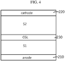
- FIG. 4 is a cross-sectional view illustrating an organic light emitting device in accordance with second embodiment of the present invention.
- an organic light emitting device in accordance with the second embodiment of the present invention has a plurality of stacks S1, S2, ..., each stack including the hole transport layer 130the trapping layer 140, the electron blocking layer 150, the organic emitting layer 160 and the electron transport layer 170 in FIG 1 .
- a charge generation layer 230 may be provided between stacks S1 and S2.
- the organic light emitting device in accordance with the second embodiment of the present invention may have 3 or more stacks and each charge generation layer CGL may be positioned between two stacks.
- the light emitting device in accordance with the second embodiment of the present invention has similar advantages to have the trapping layer 140 between thin hole transport layer 130 and the electron blocking layer 150 in the stack S1, S2..., such as the light emitting device in accordance with the first embodiment of the present invention.
- the comparative example corresponds to the structure except the trapping layer 140 in FIG 1 .
- the comparative example is understood by FIG. 4 .
- FIG. 5 is a band diagram of an organic light emitting device in accordance with the comparative example.
- the organic light emitting device in accordance with the comparative example there are a hole transport layer 30, an electron blocking layer 50, an organic emitting layer 60 and an electron transport layer 70 between a anode and a cathode.
- the electron blocking layer 50 is positioned adjacent to the organic emitting layer 60, electrons escaped from the organic emitting layer 60 may be disposed between the hole transport layer 30 and the electron blocking layer 50, and escaped electrons can be easily excited and can be combined with holes to cause leakage of emission in the hole transport layer 30 in addition to the organic emitting layer 60. Also, some moved electrons into the hole transport layer 30 deteriorate the hole transport layer 30, it causes to lower a lifespan of the organic light emitting device of the comparative example.
- the energy bandgap of the electron blocking layer 50 is 2eV to 3eV and it is difficult to complex a material having a broad energy bandgap for the electron blocking layer.
- the present invention uses structural change in the organic light emitting device by introducing the trapping layer 140 between the hole transport layer 130 and the electron blocking layer 150 to overcome material limit of the electron blocking layer.
- characteristic between time-luminance and driving voltages are compared by without a trapping layer or varying the thicknesses of the trapping layer as 5 ⁇ , 10 ⁇ , and 20 ⁇ .
- FIG. 6 is a graph showing lifespans of an organic light emitting device in accordance with the experimental examples by varying the thicknesses of the trapping layer.
- lifespans are increased in all experimental examples and the lifespan is more increased when the thickness of the trapping layer 140 becomes thicker.
- a lifespan in the comparative example having no trapping layer is less than the lifespan even in the experimental example of the thickness 5 ⁇ of the trapping layer 140 being least experimental example.
- the graph illustrates a time that a luminance is changed from an initial state to 95% luminance.
- FIG. 7 is a graph showing driving voltages of an organic light emitting device in accordance with the experimental examples by varying the thicknesses of the trapping layer.
- the driving voltages are lowered than that of the comparative example by 0.1V or more.
- the driving voltage is rather increased than that of the comparative example.
- the thickness of the trapping layer is in a range of 5 ⁇ to 10 ⁇ .
- the organic light emitting display of the present invention applies the organic light emitting device of the present invention provided at each sub-pixel.
- FIG. 8 is a cross-sectional view illustrating an organic light emitting display in accordance with the present invention.
- the organic light emitting display in accordance with the present invention includes a substrate 100 including a plurality of sub-pixels, thin film transistors (TFTs) of the respective sub-pixels being provided on the substrate 100, and organic light emitting devices (OLED) having anodes 110 and cathodes 120.
- TFTs thin film transistors
- OLED organic light emitting devices
- the anode 110 or the cathode 120 of each organic light emitting device is connected to each TFT.
- FIG. 8 illustrates one sub-pixel, sub-pixels having the same shape are substantially arranged in a matrix on the substrate 100.
- the thin film transistor includes a gate electrode 101 provided in a designated region on the substrate 100, a gate insulating film 102 formed on the substrate 100 so as to cover the gate electrode 101, a semiconductor layer 103 formed on the gate insulating film 102 so as to correspond to the gate electrode 101, and a source electrode 104a and a drain electrode 104b formed at both sides of the semiconductor layer 103.
- an inorganic protective film 105 and an organic protective film 106 are sequentially provided to cover the source electrode 104a and the drain electrode 104b, and the anode 110 or the cathode 120 is connected to the drain electrode 104b via a contact hole 1060 formed through the organic protective film 106 and the inorganic protective film 105 to expose a part of the drain electrode 104b.
- an organic stack 300 in which a hole transport layer (HTL) 130, a trapping layer (CNL) 140, an electron blocking layer (EBL) 150, an organic emitting layer (EML) 160 and an electron transport layer (ETL) 170 are sequentially deposited, is formed on the anode 110, and the cathode 120 is provided on the organic stack 300, similarly as for the stack S shown in FIG 1 .
- the organic stack 300 may be replaced with the stack structure shown in FIG. 4 .
- an organic stack in which the above-described elements are provided in reverse order, is provided. That is, an electron transport layer ETL, an organic emitting layer EML, an electron blocking layer EBL, a trapping layer CNL, and a hole transport layer HTL are sequentially deposited on the cathode, and then an anode is formed on the hole transport layer HTL.
- a hole injection layer may be further provided between the anode 110 and a hole transport layer (HTL) 130, and an electron injection layer may be further provided between the electron transport layer (ETL) 170 and the cathode 120.
- HTL hole transport layer
- ETL electron transport layer
- this figure illustrates a bank 107 provided to define an emission zone
- the bank 107 may be omitted and the emission zone may be defined by other structures or the organic stack and the cathode 120 may be provided in common in all sub-pixels and colors of the sub-pixels may be discriminated by color filters.
- FIG. 8 illustrates the organic light emitting device in accordance with the embodiment shown in FIG 1
- the disclosure is not limited thereto and the organic light emitting device in accordance with the embodiment shown in FIG. 4 , in which a plurality of stacks is provided between an anode and a cathode, may be provided.
- the above-described organic light emitting display may achieve color expression by emitting different colors of light through the organic emitting layers of the respective sub-pixels, or achieve color expression by adding a color filter layer to a light emitting portion of a common organic emitting layer.
- Such an organic light emitting display including the above-described organic light emitting device may have the same effects as the above-described organic light emitting device.
- an organic light emitting device and an organic light emitting display using the same in accordance with one embodiment of the present invention have effects below.
- the present invention provides a trapping layer between the hole transport layer and the electron blocking layer and uses the material for the trapping layer having a low LUMO energy level similar to the HOMO levels of the hole transport layer and the electron blocking layer, thus the energy level of electrons into the trapping layer is lowered to a ground state and it can blocks that the electrons escaped from the electron blocking layer is excited. Also, it prevent deterioration of the hole transport layer and prevent increasing the driving voltage.
- the holes when the holes are transported from the hole transport layer to the organic emitting layer, the holes cannot react the electrons of a low energy level in the trapping layer, thus it blocks leakage of emission outside of the organic emitting layer.
- the trapping layer functions as a charge generation layer, and helps increase of a lifespan of the organic light emitting device or the organic light emitting display.
Landscapes
- Physics & Mathematics (AREA)
- Optics & Photonics (AREA)
- Geometry (AREA)
- Engineering & Computer Science (AREA)
- Microelectronics & Electronic Packaging (AREA)
- Electromagnetism (AREA)
- Electroluminescent Light Sources (AREA)
- Devices For Indicating Variable Information By Combining Individual Elements (AREA)
- Control Of El Displays (AREA)
- Control Of Indicators Other Than Cathode Ray Tubes (AREA)
Abstract
Description
- This application claims the benefit of
Korean Patent Application No. 10-2016-0097549, filed on July 29, 2016 - The present invention relates to an organic light emitting device, and more particularly, to an organic light emitting device, which provides a certain layer between a hole transport layer and an electron blocking layer so as to increase lifespan and decrease a driving voltage, and an organic light emitting display using the same.
- As the information age has arrived, the field of displays visually expressing electrical information signals has rapidly developed and, in order to satisfy such a trend, various flat display devices having excellent performance, such as thin thickness, light weight and low power consumption have been researched as a substitute for a conventional cathode ray tube (CRT).
- As representative examples of flat display devices, there are liquid crystal displays (LCDs), plasma display panels (PDPs), field emission displays (FEDs), and organic light emitting device (OLED) displays, etc.
- Thereamong, an organic light emitting display requires no separate light source and has been considered as an application having competitiveness so as to achieve compactness of a device and good color reproduction.
- The organic light emitting display includes a plurality of sub-pixels, and each sub-pixel includes an organic light emitting device (OLED: sometimes, OLED is used for 'organic light emitting diode') consisting of an anode and a cathode, and a plurality of organic layers between the anode and the cathode. The organic light emitting device emits light when a current is applied between the anode and the cathode.
- At least one layer of the organic layers between the anode and the cathode is an organic light emitting layer. Holes and electrons from the anode and cathode are injected into the organic light emitting layer and are combined with each other in the organic light emitting layer, thus generating excitons. When the generated excitons are changed from an excited state to a ground state, the organic light emitting diode emits light. For example, a basic structure of the organic light emitting diode includes an anode and a cathode, and a hole injection layer, a hole transport layer, an organic light emitting layer, an electron transport layer and electron injection layer sequentially stacked from the anode, between the anode and the cathode.
- Meanwhile, it is preferable that the electrons and the holes are contained in the organic light emitting diode for high emission efficiency. For this, it is suggested to provide an electron blocking layer (EBL) between the hole transport layer and the organic light emitting layer such that the electron blocking layer prevents the electrons from leaking in the organic light emitting layer when the current is applied between the anode and the cathode.
- However, it is inevitable that some electrons from the organic light emitting layer escape to the hole transport layer by providing the electron blocking layer. Thus the moved electrons is remained and cause deterioration of the hole transport layer and higher driving voltage. Accordingly, there is a difficulty to realize a certain life time.
- Also, the electron blocking layer requires a broad bandgap for smoothly transporting holes and blocking electrons, but known materials used for the electron blocking layer have high LUMO (Lowest Unoccupied Molecular Orbital) and high HOMO (Highest Occupied Molecular Orbital) and thus have a narrow bandgap. Therefore, the organic light emitting device having the electron blocking layer of known material, has problems such as insufficient hole injection/transportation of holes into the light emitting layer and high driving voltage.
- Accordingly, the present invention is directed to an organic light emitting device and an organic light emitting display using the same that substantially obviate one or more problems due to limitations and disadvantages of the related art.
- An object of the present invention is to provide an organic light emitting device, which provides a certain layer between a hole transport layer and an electron blocking layer so as to increase lifespan and decrease a driving voltage, and an organic light emitting display using the same.
- Additional advantages, objects, and features of the invention will be set forth in part in the description which follows and in part will become apparent to those having ordinary skill in the art upon examination of the following or may be learned from practice of the invention. The objectives and other advantages of the invention may be realized and attained by the structure particularly pointed out in the written description and claims hereof as well as the appended drawings.
- An organic light emitting device even the structure including the electron blocking layer can simultaneously capture escaped electrons and prevent high driving voltage and increase lifespan by providing a certain layer.
- To achieve these objects and other advantages and in accordance with the purpose of the invention, as embodied and broadly described herein, an organic light emitting device according to claim 1 is provided. Further embodiments are described in the dependent claims. In one aspect of the present invention, an organic light emitting device includes an anode, a hole transport layer on the anode, an electron blocking layer on the hole transport layer, an organic emitting layer contacting the electron blocking layer, and an electron transport layer contacting the organic emitting layer, a cathode on the electron transport layer and a trapping layer between the hole transport layer and the electron blocking layer, wherein a LUMO energy level of the trapping layer differs from a HOMO energy level of the electron blocking layer within a range of 1eV or is equal to the HOMO energy level of the electron blocking layer.
- The LUMO energy level of the trapping layer may differ from a HOMO energy level of the hole transport layer within a range of 1eV or be equal to the HOMO energy level of the hole transport layer.
- The LUMO energy level of the trapping layer may be lower than the HOMO energy level of the electron blocking layer.
- The LUMO energy level of the trapping layer may be between the HOMO energy level of the hole transport layer and the electron blocking layer or equal to the HOMO energy level of the hole transport layer and the electron blocking layer. The HOMO energy level of the electron blocking layer may be higher than a HOMO energy level of the organic emitting layer by 0.4eV.
- A thickness of the trapping layer may be less than or equal to 1/5 times of a thickness of hole transport layer. The thickness of the trapping layer may be about 5Å to 10Å.
- Also, the electrons escaped from the electron blocking layer toward the hole transport layer may be captured into the trapping layer when voltages are applied to the anode and the cathode.
- In another aspect of the present invention, an organic light emitting display includes a substrate having a plurality of subpixels, a thin-film transistor provided in each subpixel on the substrate and the above organic light emitting device at each sub-pixel, wherein each thin-film transistor is connected to one of the anode and the cathode, and wherein a LUMO energy level of the trapping layer differs from a HOMO energy level of the electron blocking layer within a range of 1eV or is equal to the HOMO energy level of the electron blocking layer.
- Even though there are holes transported from the hole transport layer into the trapping layer, the holes cannot combine with the electron having low energy level. Also, even though holes in the trapping layer partially combines with the electrons, the combined pairs in the trapping layer cannot emit due to being non-excited level and cannot cause any emission in the organic light emitting device.
- Also, escaped electrons from the electron blocking layer can be captured in the trapping layer, and holes occupy the empty site in the electron blocking layer due to escaped electrons. Thus it makes smoothly transporting holes into the light emitting layer, the trapping layer functions as a charge generation layer herein. Accordingly, a lifespan of the organic light emitting device is increased.
- It is to be understood that both the foregoing general description and the following detailed description of the present invention are exemplary and explanatory and are intended to provide further explanation of the invention as claimed.
- The accompanying drawings, which are included to provide a further understanding of the invention and are incorporated in and constitute a part of this application, illustrate embodiment(s) of the invention and together with the description serve to explain the principle of the invention. In the drawings:
-
FIG. 1 is a cross-sectional view illustrating an organic light emitting device in accordance with first embodiment of the present invention. -
FIG. 2 is a band diagram of an organic light emitting device in accordance with the present invention. -
FIG. 3 is a drawing to specifically show working between the hole transport layer and the electron blocking layer. -
FIG. 4 is a cross-sectional view illustrating an organic light emitting device in accordance with second embodiment of the present invention. -
FIG. 5 is a band diagram of an organic light emitting device in accordance with the comparative example. -
FIG. 6 is a graph showing lifespans of an organic light emitting device in accordance with the experimental examples by varying the thicknesses of the trapping layer. -
FIG. 7 is a graph showing driving voltages of an organic light emitting device in accordance with the experimental examples by varying the thicknesses of the trapping layer. -
FIG. 8 is a cross-sectional view illustrating an organic light emitting display in accordance with the present invention. - Reference will now be made in detail to the preferred embodiments of the present invention, examples of which are illustrated in the accompanying drawings. However, the disclosure of the invention is not limited to the embodiments set forth therein and may be variously modified. It should be understood, however, that there is no intent to limit the invention to the particular forms disclosed, but on the contrary, the invention is to cover all modifications, equivalents, and alternatives falling within the spirit and scope of the invention as defined by the claims.
- Shapes, sizes, rates, angles, numbers, etc. illustrated in the drawings to describe the embodiments of the present invention are exemplary and thus are not limited to the drawings. In the drawings, the same or similar elements are denoted by the same reference numerals even though they are depicted in different drawings. In the following description of the present invention, a detailed description of known functions and configurations incorporated herein will be omitted when it may make the subject matter of the present invention rather unclear. In the following description of the embodiments, the terms "including", "having", "consisting of", etc. will be interpreted as indicating the presence of other elements, unless stated otherwise, and do not exclude presence of the corresponding elements. In addition, when a singular element is stated, the element may be provided in plural, unless state otherwise.
- In interpretation of elements included in the embodiments of the present invention, the elements will be interpreted as having error ranges, unless stated otherwise.
- It will be understood that when positional relations between two elements are described, for example, when an element is referred to as being "on", "above", "under" or "aside" another element, intervening elements may also be present between the two elements, unless the term "just" or "directly" is used.
- Further, it will be understood that when temporal relations between incidents are described, for example, the temporal order, such as "after", "subsequent to", "next" or "before", is described, the incidents may not be continuous, unless the term "just" or "directly" is used.
- It will be understood that, although the terms "first", "second", etc. may be used herein to describe various elements, these elements should not be limited by these terms. Therefore, in the following description of the embodiments, an element modified by the term "first" may be the same as an element modified by the term "second", unless stated otherwise.
- Respective characteristics of the embodiments of the present invention may be partially or generally combined or mixed, or be technically interlocked and driven, and the embodiments may be independently executed or be executed together in connection with each other.
- Firstly, an organic light emitting device of present invention is explained.
-
FIG. 1 is a cross-sectional view illustrating an organic light emitting device in accordance with first embodiment of the present invention. - As shown in
FIG. 1 , the organic light emitting device in accordance with first embodiment of the present invention includes ananode 110, ahole transport layer 130 on theanode 110, anelectron blocking layer 150 on thehole transport layer 130, an organic emittinglayer 160 contacting theelectron blocking layer 150, and anelectron transport layer 170 contacting the organic emittinglayer 160, acathode 120 on theelectron transport layer 170 and atrapping layer 140 between thehole transport layer 130 and theelectron blocking layer 150. A LUMO energy level of thetrapping layer 140 differs from a HOMO energy level of theelectron blocking layer 150 within a range of 1eV or is equal to the HOMO energy level of theelectron blocking layer 150. - Also, a
hole injection layer 125 may be further provided between theanode 110 and thehole transport layer 130 to increase efficiency of hole injection. And anelectron injection layer 180 may be further provided between theelectron transport layer 170 and theanode 120 to increase efficiency of electron injection. Thehole injection layer 125 and theelectron injection layer 180 may be selectively provided or may same function by mixing hole injection material into the hole transport layer and electron injection material into the electron transport layer, respectively. - The
trapping layer 140 between thehole transport layer 130 and theelectron blocking layer 150 can trap escaped electrons from theelectron blocking layer 150, and help to block the electrons from the organic emittinglayer 160 with theelectron blocking layer 150. Even though theelectron blocking layer 150 is provided to block the electrons from the organic emittinglayer 160, theelectron blocking layer 150 cannot singly block total escape of electrons. Thetrapping layer 140 of the present invention has lower LUMO (Lowest Unoccupied Molecular Orbital) and is provided between thehole transport layer 130 and theelectron blocking layer 150. Therefore, escaped electrons from theelectron blocking layer 150 are captured as lower energy level in thetrapping layer 140. That is, electrons escaped from theelectron blocking layer 150 toward thehole transport layer 130 are captured into the trapping layer when voltages are applied to theanode 110 and thecathode 120. - The described as 'S' in
FIG. 1 means essential organic stack between theanode 110 andcathode 120, and layers in the organic stack S are organic layers. - Energy band of the present invention is explained in the following description.
-
FIG. 2 is a band diagram of an organic light emitting device in accordance with the present invention andFIG. 3 is a drawing to specifically show working between the hole transport layer and the electron blocking layer. - As shown in
FIG. 2 , firstly, a LUMO energy level of theelectron blocking layer 150 is higher than a LUMO energy level of the organic emittinglayer 160, it is difficult of the electrons in the organic emittinglayer 160 to escape towardhole transport layer 130. - However, if a current between the
anode 110 and thecathode 120 and difference of LUMOs between theelectron blocking layer 150 and the organic light emitting is within a range of 1eV, it is inevitable from theelectron blocking layer 150 of the electrons to escape. In particular, the amount of escaped electrons from theelectron blocking layer 150 becomes more when the current between theanode 110 and thecathode 120 becomes higher. - Also, the escaped electrons from the organic emitting layer do not contain in the electron blocking layer, can move toward adjacent layer. In the present invention, the
trapping layer 140 contacts theelectron transport layer 150, the escaped electrons are captured in the trapping layers 140 and thus thetrapping layer 140 blocks that the electrons moves into thehole transport layer 130. - The LUMO energy level of the
trapping layer 140 is equal to or similar to the HOMO energy level HOMO2 of theelectron blocking layer 150. Even though there are escaped electrons from theelectron blocking layer 150, energy level of the escaped electrons is lowered as a low energy level and the escaped electrons are captured into thetrapping layer 140 and thus an energy level of the electrons captures in thetrapping layer 140 is non-exited state. Therefore, although holes from thehole transport layer 130 and escaped electrons are partially combined in thetrapping layer 140, nevertheless a non-emission state is maintained in thetrapping layer 140. Although electrons of a low level are partially moved into thehole transport layer 130, the holes cannot cause deterioration of the hole transport layer and increasing a driving voltage, and hole transporting efficiency is highly maintained since holes occupies the depleted state of electrons in the organic emittinglayer 160. -
FIG. 3 shows the LUMO energy level LUMO of thetrapping layer 140 is similar to the HOMO energy level HOMO1 of thehole transport layer 130. The LUMO energy level LUMO of thetrapping layer 140 is not limited to such, the LUMO energy level LUMO of thetrapping layer 140 may differ from the HOMO energy level HOMO1 of thehole transport layer 130 within a range of 1eV, and the LUMO energy level LUMO of thetrapping layer 140 may differ from the HOMO energy level HOMO2 of theelectron blocking layer 140 within a range of 1eV or be same to the HOMO energy level HOMO2 of theelectron blocking layer 140. That is, the LUMO energy level LUMO of thetrapping layer 140 may be lower than the HOMO energy level HOMO2 of theelectron blocking layer 150 within 1eV or may be higher than the HOMO energy level HOMO2 of theelectron blocking layer 150 within 1eV. That is, a range of the LUMO energy level LUMO of thetrapping layer 140 is 'the HOMO energy level HOMO2 of the electron blocking layer 150-1eV' to 'the HOMO energy level HOMO2 of theelectron blocking layer 150+1eV.' It is preferable that the LUMO energy level LUMO of thetrapping layer 140 is lower than the HOMO energy level HOMO2 of theelectron blocking layer 150 such that the energy level of the escaped electrons is lowered. - Herein, the LUMO energy levels, HOMO energy levels are all negative values and a LUMO energy level or a HOMO energy level located at an upper in the band diagram means a lower value as absolute value. In the description, each value of the LUMO energy levels, HOMO energy levels is compared as each substantial negative value shown in the band diagram.
- Meanwhile, each energy bandgap of the
hole transport layer 130, thetrapping layer 140 and theelectron blocking layer 150 is 2eV or more, thus the HOMO energy level oftrapping layer 140 is lower than the HOMO energy level HOMO2 of theelectron blocking layer 150. - The reason why the LUMO energy level LUMO of the
trapping layer 140 is similar to the HOMO energy level HOMO1 of thehole transport layer 130 and the HOMO energy level HOMO 2 of theelectron blocking layer 150 is to lower the energy level of the escaped electrons as a non-excited state and to move the electrons into thetrapping layer 140 and block transporting electrons into thehole transport layer 130 even though there is partially escaped electrons from theelectron blocking layer 150 into thehole transport layer 130. - Meanwhile, when a current is applied between an
anode 110 and acathode 120, some electrons may be combined with the holes at an interfacial between thetrapping layer 140 and thehole transport layer 130. However, the electrons from and in thetrapping layer 140 has a low energy level, combined hole and electron at the interfacial between thetrapping layer 140 and thehole transport layer 130 has no excited level and thus combined hole and electron at the interfacial between thetrapping layer 140 and thehole transport layer 130 cannot emit. And although not combined electron are partially moved to thehole transport layer 130, electrons of the low energy level cannot deteriorate thehole transport layer 130 and cannot increase the driving voltage. Also, the state that electrons escape from in the organic emittinglayer 160 can be occupied with holes, holes through thehole transport layer 130, trappinglayer 140 and theelectron blocking layer 150 are smoothly provided into the organic emittinglayer 160, thus recombination of holes and electrons in the organic emittinglayer 160 is increased and it causes to climb an emission efficiency. In this case, thetrapping layer 140 also functions as a charge generation. - As shown in
FIG. 3 , it is preferable that the LUMO energy level LUMO of thetrapping layer 140 is lower than the HOMO energy level HOMO2 of theelectron blocking layer 150 such that the energy level of the escaped electrons from theelectron blocking layer 150 near to the HOMO energy level HOMO2 of theelectron blocking layer 150 is lowered below the LUMO energy level LUMO of thetrapping layer 140. In this case, the HOMO energy level HOMO 1 of thehole transport layer 130 can be slightly lower than the HOMO energy level HOMO 2 of theelectron blocking layer 150 and also the HOMO energy level HOMO 1 is lower than the LUMO energy level LUMO of thetrapping layer 140 as shown inFIG 3 . - It is preferable that the LUMO energy level LUMO of the
trapping layer 140 is between the HOMO energy level HOMO1 of thehole transport layer 130 and the HOMO energy level HOMO2 of theelectron blocking layer 150 or same to the HOMO energy level HOMO1 of thehole transport layer 130 or the HOMO energy level HOMO2 of theelectron blocking layer 150 in view of effectively trapping the escaped electrons and trapping holes. - For example, the HOMO energy level HOMO1 of the
hole transport layer 130 is -5.6eV to -5.4eV, and the HOMO energy level HOMO2 of theelectron blocking layer 150 is -5.3eV to -5.0eV. In this case, the LUMO energy level LUMO of thetrapping layer 140 is -5.6eV to -5.0eV. - In the organic light emitting device, it is effective that the HOMO energy level HOMO 2 is higher than the HOMO energy level of the organic emitting
layer 160 by 0.4eV. This means to solve material limit of theelectron blocking layer 150 having a narrow bandgap by providing thetrapping layer 140. If the electron blocking layer is in contact with the hole transport layer without a trapping layer and some electrons are escaped from the electron blocking layer, the escaped electrons is easily moved into the hole transport layer and thus the escaped electrons having a high energy level causes deterioration of the hole transport layer. On the contrary, the organic light emitting device in the present invention has thetrapping layer 140 having a low LUMO energy level LUMO similar or same to the HOMO energy level HOMO2 of theelectron blocking layer 150, thus the escaped electrons can be captured in thetrapping layer 140, the escaped electrons are hardly moved into thehole transport layer 130. Accordingly, it makes to prevent deterioration of thehole transport layer 130 caused from the accumulation of electrons at the interfacial of thehole transport layer 130 and it is expected to increase a lifespan. - For example, material for the
trapping layer 140 may be any one of HATCN, F4TCNQ and MoO3 to meet the above LUMO energy level LUMO and material for thehole transport layer 130 may be any one of N,N'-bis-(1-naphthalenyl)-N,N'-bis-phenyl-(1,1'biphenyl)-4,4'-diamine (NPB, also referred to as N,N'-bis(naphthalene-1-yl)-N,N'-bis(phenyl)benzidine (NPD)), α -NPD, BBTC, NPhen, or a derivative thereof to meet the above HOMO energy level HOMO1. Also, material for theelectron blocking layer 150 may be any one of TAPC, TCTA or a derivative thereof to meet the above HOMO energy level HOMO2. - The materials for the
trapping layer 140, thehole transport layer 130 and theelectron blocking layer 150 are not limited to the above mentioned examples, and may be replaced with another material which can meet the energy band diagram ofFIGs. 2 and3 . - Meanwhile, it is preferable that a thickness of the
trapping layer 140 may be less than or equal to 1/5 times of a thickness ofhole transport layer 130, or more preferable that a thickness of thetrapping layer 140 is less than 1/10 times of a thickness ofhole transport layer 130. Since the thickness of thetrapping layer 140 is too thin to selectively function as trapping the escaped electrons, thus transportability of hole is maintained from thehole transport layer 130 to the organic emittinglayer 160. For example, the thickness of thehole transport layer 130 is 100Å to 2000Å, the thickness of theelectron blocking layer 150 is 30Å to 300Å. That is, thehole transport layer 130 and theelectron blocking layer 150 are thicker than the thickness of thetrapping layer 140 under 10Å, thus a velocity of hole transporting is maintained to ignore thetrapping layer 140 between thehole transport layer 130 to the organic emittinglayer 160. - It is preferable that the thickness of the
trapping layer 140 is about 5Å to 10Å. If the thickness of thetrapping layer 140 is smaller than 5Å, thetrapping layer 140 cannot properly trap the escaped electrons, and if the thickness of thetrapping layer 140 is larger than 10Å, the driving voltage may be increased. For this, it is more explained by experimental examples later in the description. -
FIG. 4 is a cross-sectional view illustrating an organic light emitting device in accordance with second embodiment of the present invention. - As shown in
FIG. 4 , an organic light emitting device in accordance with the second embodiment of the present invention has a plurality of stacks S1, S2, ..., each stack including the hole transport layer 130the trappinglayer 140, theelectron blocking layer 150, the organic emittinglayer 160 and theelectron transport layer 170 inFIG 1 . Acharge generation layer 230 may be provided between stacks S1 and S2. Differently fromFIG. 4 , the organic light emitting device in accordance with the second embodiment of the present invention may have 3 or more stacks and each charge generation layer CGL may be positioned between two stacks. - The light emitting device in accordance with the second embodiment of the present invention has similar advantages to have the
trapping layer 140 between thinhole transport layer 130 and theelectron blocking layer 150 in the stack S1, S2..., such as the light emitting device in accordance with the first embodiment of the present invention. - Hereinafter, referring Drawings and Examples, comparative example and experimental examples are compared.
- The comparative example corresponds to the structure except the
trapping layer 140 inFIG 1 . The comparative example is understood byFIG. 4 . -
FIG. 5 is a band diagram of an organic light emitting device in accordance with the comparative example. - As shown in
FIG. 5 , the organic light emitting device in accordance with the comparative example, there are ahole transport layer 30, anelectron blocking layer 50, an organic emittinglayer 60 and anelectron transport layer 70 between a anode and a cathode. - In the comparative example, although the
electron blocking layer 50 is positioned adjacent to the organic emittinglayer 60, electrons escaped from the organic emittinglayer 60 may be disposed between thehole transport layer 30 and theelectron blocking layer 50, and escaped electrons can be easily excited and can be combined with holes to cause leakage of emission in thehole transport layer 30 in addition to the organic emittinglayer 60. Also, some moved electrons into thehole transport layer 30 deteriorate thehole transport layer 30, it causes to lower a lifespan of the organic light emitting device of the comparative example. - It is ideal to use a material to have a broad energy bandgap for the
electron blocking layer 50, which has a high LUMO energy level and a low LUMO energy level, but it is hardly to find the material for theelectron blocking layer 50. Substantially, the energy bandgap of theelectron blocking layer 50 is 2eV to 3eV and it is difficult to complex a material having a broad energy bandgap for the electron blocking layer. The present invention uses structural change in the organic light emitting device by introducing thetrapping layer 140 between thehole transport layer 130 and theelectron blocking layer 150 to overcome material limit of the electron blocking layer. - In the comparative example and experimental examples, characteristic between time-luminance and driving voltages are compared by without a trapping layer or varying the thicknesses of the trapping layer as 5Å, 10Å, and 20 Å.
-
FIG. 6 is a graph showing lifespans of an organic light emitting device in accordance with the experimental examples by varying the thicknesses of the trapping layer. - As shown in
FIG. 6 , lifespans are increased in all experimental examples and the lifespan is more increased when the thickness of thetrapping layer 140 becomes thicker. On the contrary, a lifespan in the comparative example having no trapping layer is less than the lifespan even in the experimental example of the thickness 5Å of thetrapping layer 140 being least experimental example. - The graph illustrates a time that a luminance is changed from an initial state to 95% luminance.
-
FIG. 7 is a graph showing driving voltages of an organic light emitting device in accordance with the experimental examples by varying the thicknesses of the trapping layer. - As shown in
FIG. 7 , in the cases of providing thetrapping layer 140 having the thickness as 5Å and 10Å, the driving voltages are lowered than that of the comparative example by 0.1V or more. However, the case of providing thetrapping layer 140 having the thickness as 20Å, the driving voltage is rather increased than that of the comparative example. - That is, in order to together increase the lifespan and lower the driving voltage, it is preferable that the thickness of the trapping layer is in a range of 5Å to 10 Å.
- Meanwhile, the organic light emitting display of the present invention applies the organic light emitting device of the present invention provided at each sub-pixel.
-
FIG. 8 is a cross-sectional view illustrating an organic light emitting display in accordance with the present invention. - As exemplarily shown in
FIG. 8 , the organic light emitting display in accordance with the present invention includes asubstrate 100 including a plurality of sub-pixels, thin film transistors (TFTs) of the respective sub-pixels being provided on thesubstrate 100, and organic light emitting devices (OLED) havinganodes 110 andcathodes 120. Here, theanode 110 or thecathode 120 of each organic light emitting device is connected to each TFT. AlthoughFIG. 8 illustrates one sub-pixel, sub-pixels having the same shape are substantially arranged in a matrix on thesubstrate 100. - Here, the thin film transistor includes a
gate electrode 101 provided in a designated region on thesubstrate 100, agate insulating film 102 formed on thesubstrate 100 so as to cover thegate electrode 101, asemiconductor layer 103 formed on thegate insulating film 102 so as to correspond to thegate electrode 101, and asource electrode 104a and adrain electrode 104b formed at both sides of thesemiconductor layer 103. - Further, an inorganic
protective film 105 and an organicprotective film 106 are sequentially provided to cover thesource electrode 104a and thedrain electrode 104b, and theanode 110 or thecathode 120 is connected to thedrain electrode 104b via acontact hole 1060 formed through the organicprotective film 106 and the inorganicprotective film 105 to expose a part of thedrain electrode 104b. - For example, if the
anode 110 is connected to thedrain electrode 104b, anorganic stack 300, in which a hole transport layer (HTL) 130, a trapping layer (CNL) 140, an electron blocking layer (EBL) 150, an organic emitting layer (EML) 160 and an electron transport layer (ETL) 170 are sequentially deposited, is formed on theanode 110, and thecathode 120 is provided on theorganic stack 300, similarly as for the stack S shown inFIG 1 . As circumstances require, theorganic stack 300 may be replaced with the stack structure shown inFIG. 4 . - On the other hand, if the
cathode 120 is connected to thedrain electrode 104b, an organic stack, in which the above-described elements are provided in reverse order, is provided. That is, an electron transport layer ETL, an organic emitting layer EML, an electron blocking layer EBL, a trapping layer CNL, and a hole transport layer HTL are sequentially deposited on the cathode, and then an anode is formed on the hole transport layer HTL. - In some cases, a hole injection layer may be further provided between the
anode 110 and a hole transport layer (HTL) 130, and an electron injection layer may be further provided between the electron transport layer (ETL) 170 and thecathode 120. - Further, although this figure illustrates a
bank 107 provided to define an emission zone, thebank 107 may be omitted and the emission zone may be defined by other structures or the organic stack and thecathode 120 may be provided in common in all sub-pixels and colors of the sub-pixels may be discriminated by color filters. - Moreover, although
FIG. 8 illustrates the organic light emitting device in accordance with the embodiment shown inFIG 1 , the disclosure is not limited thereto and the organic light emitting device in accordance with the embodiment shown inFIG. 4 , in which a plurality of stacks is provided between an anode and a cathode, may be provided. - The above-described organic light emitting display may achieve color expression by emitting different colors of light through the organic emitting layers of the respective sub-pixels, or achieve color expression by adding a color filter layer to a light emitting portion of a common organic emitting layer.
- Such an organic light emitting display including the above-described organic light emitting device may have the same effects as the above-described organic light emitting device.
- As apparent from the above description, an organic light emitting device and an organic light emitting display using the same in accordance with one embodiment of the present invention have effects below.
- First, the present invention provides a trapping layer between the hole transport layer and the electron blocking layer and uses the material for the trapping layer having a low LUMO energy level similar to the HOMO levels of the hole transport layer and the electron blocking layer, thus the energy level of electrons into the trapping layer is lowered to a ground state and it can blocks that the electrons escaped from the electron blocking layer is excited. Also, it prevent deterioration of the hole transport layer and prevent increasing the driving voltage.
- Also, when the holes are transported from the hole transport layer to the organic emitting layer, the holes cannot react the electrons of a low energy level in the trapping layer, thus it blocks leakage of emission outside of the organic emitting layer.
- Further, escaped electrons from the electron blocking layer can be captured in the trapping layer and the empty sites of the electron blocking layer and the organic emitting layer addition due to electrons' escaping is occupied with holes and thus it helps that holes are easily transported from the hole transport layer into the organic emitting layer. In this case, the trapping layer functions as a charge generation layer, and helps increase of a lifespan of the organic light emitting device or the organic light emitting display.
Claims (9)
- An organic light emitting device comprising:an anode (110);a hole transport layer (130) on the anode (110);an electron blocking layer (150) on the hole transport layer (130), an organic emitting layer (160) contacting the electron blocking layer (150), and an electron transport layer (170) contacting the organic emitting layer (160);a cathode (120) on the electron transport layer (170); anda trapping layer (140) between the hole transport layer (130) and the electron blocking layer (150), wherein a LUMO energy level of the trapping layer (140) differs from a HOMO energy level of the electron blocking layer (150) within a range of 1eV or is equal to the HOMO energy level of the electron blocking layer (150).
- The organic light emitting device according to claim 1, wherein the LUMO energy level of the trapping layer (140) differs from a HOMO energy level of the hole transport layer (130) within a range of 1eV or is equal to the HOMO energy level of the hole transport layer (130).
- The organic light emitting device according to claim 1 or 2, wherein the LUMO energy level of the trapping layer (140) is lower than the HOMO energy level of the electron blocking layer (150).
- The organic light emitting device according to claim 2, wherein the LUMO energy level of the trapping layer (140) is between the HOMO energy level of the hole transport layer (130) and the electron blocking layer (150) or equal to the HOMO energy level of the hole transport layer (130) and the electron blocking layer (150).
- The organic light emitting device according to claim 4, wherein the HOMO energy level of the electron blocking layer (150) is higher than a HOMO energy level of the organic emitting layer (160) by 0.4eV.
- The organic light emitting device according to any one of claims 1 to 5, wherein a thickness of the trapping layer (140) is less than or equal to 1/5 times of a thickness of the hole transport layer (130).
- The organic light emitting device according to claim 6, wherein the thickness of the trapping layer (140) is about 5Å to 10Å.
- The organic light emitting device according to any one of claims 1 to 7, wherein electrons escaped from the electron blocking layer (150) toward the hole transport layer (130) are captured into the trapping layer (140) when voltages are applied to the anode (110) and the cathode (120).
- An organic light emitting display comprising:a substrate (100) having a plurality of subpixels;each subpixel of the plurality of subpixels comprising a thin-film transistor and an organic light emitting device (OLED) according to any one of claims 1 to 8,wherein the thin-film transistor is connected to one of the anode (110) and the cathode (120) of the organic light emitting device.
Applications Claiming Priority (1)
| Application Number | Priority Date | Filing Date | Title |
|---|---|---|---|
| KR1020160097549A KR102620084B1 (en) | 2016-07-29 | 2016-07-29 | Organic Light Emitting Element and Organic Light Emitting Display Device Using the Same |
Publications (2)
| Publication Number | Publication Date |
|---|---|
| EP3276698A1 true EP3276698A1 (en) | 2018-01-31 |
| EP3276698B1 EP3276698B1 (en) | 2020-07-22 |
Family
ID=59387968
Family Applications (1)
| Application Number | Title | Priority Date | Filing Date |
|---|---|---|---|
| EP17182739.7A Active EP3276698B1 (en) | 2016-07-29 | 2017-07-24 | Organic light emitting device and organic light emitting display using the same |
Country Status (6)
| Country | Link |
|---|---|
| US (1) | US10483474B2 (en) |
| EP (1) | EP3276698B1 (en) |
| JP (1) | JP6715805B2 (en) |
| KR (1) | KR102620084B1 (en) |
| CN (1) | CN107665952B (en) |
| TW (1) | TWI678947B (en) |
Cited By (2)
| Publication number | Priority date | Publication date | Assignee | Title |
|---|---|---|---|---|
| CN112164753A (en) * | 2020-09-28 | 2021-01-01 | 京东方科技集团股份有限公司 | OLED device and preparation method thereof, display substrate and display device |
| US12317668B2 (en) | 2019-05-17 | 2025-05-27 | Semiconductor Energy Laboratory Co., Ltd. | Light-emitting device, light-emitting apparatus, electronic device, and lighting device |
Families Citing this family (11)
| Publication number | Priority date | Publication date | Assignee | Title |
|---|---|---|---|---|
| WO2019039562A1 (en) * | 2017-08-24 | 2019-02-28 | Agc株式会社 | Organic optoelectric element |
| TWI694628B (en) * | 2018-02-06 | 2020-05-21 | 星宸光電股份有限公司 | Electronic device |
| CN110492007B (en) * | 2018-05-14 | 2021-07-06 | 江苏三月科技股份有限公司 | Acridine compound and application thereof in organic electroluminescent device |
| CN110518136B (en) * | 2019-08-30 | 2021-12-14 | 京东方科技集团股份有限公司 | An organic electroluminescent device, display panel and display device |
| KR102782422B1 (en) * | 2019-12-31 | 2025-03-18 | 엘지디스플레이 주식회사 | Organic electronic element, display panel comprising the same and display device comprising the same |
| CN113097394B (en) | 2020-01-09 | 2022-08-12 | 京东方科技集团股份有限公司 | A kind of OLED device, display device and preparation method thereof |
| US20220246848A1 (en) * | 2020-01-23 | 2022-08-04 | Lg Chem, Ltd. | Organic light emitting device |
| CN111900257B (en) * | 2020-08-12 | 2024-07-23 | 京东方科技集团股份有限公司 | A light emitting device and a manufacturing method thereof, and a display device |
| KR20230169106A (en) | 2021-03-04 | 2023-12-15 | 한-식카드-게셀쉐프트 퓨어 안게반테 포슝 이.브이. | How to capture reference gas in a MEMS cell |
| WO2023143434A1 (en) * | 2022-01-27 | 2023-08-03 | 中国科学院理化技术研究所 | Organic electroluminescent device |
| CN115867063B (en) * | 2022-11-11 | 2024-12-06 | 昆山工研院新型平板显示技术中心有限公司 | Light emitting device, display panel and display device |
Citations (3)
| Publication number | Priority date | Publication date | Assignee | Title |
|---|---|---|---|---|
| US20130264551A1 (en) * | 2012-04-05 | 2013-10-10 | Lg Display Co., Ltd. | Tandem White Organic Light Emitting Device |
| US20150311463A1 (en) * | 2014-04-29 | 2015-10-29 | Lg Display Co., Ltd. | Organic light emitting device |
| KR20160097549A (en) | 2015-02-09 | 2016-08-18 | 청정테크주식회사 | a sludge pump |
Family Cites Families (14)
| Publication number | Priority date | Publication date | Assignee | Title |
|---|---|---|---|---|
| JPH04220995A (en) * | 1990-12-19 | 1992-08-11 | Fuji Xerox Co Ltd | Organic el element |
| JP3988196B2 (en) | 1996-09-17 | 2007-10-10 | 東洋インキ製造株式会社 | Organic electroluminescence device |
| JPH10188120A (en) | 1996-12-25 | 1998-07-21 | Sanden Corp | Automatic vending machine |
| TWI336508B (en) * | 2005-10-13 | 2011-01-21 | Ind Tech Res Inst | Memory cell, pixel structure and manufacturing process of memory cell for display |
| JP4673279B2 (en) | 2005-12-20 | 2011-04-20 | 三星モバイルディスプレイ株式會社 | Organic light emitting display device and method for manufacturing the same |
| KR100730190B1 (en) * | 2005-12-20 | 2007-06-19 | 삼성에스디아이 주식회사 | OLED display device and method of manufacturing same |
| JP2007179933A (en) * | 2005-12-28 | 2007-07-12 | Sanyo Electric Co Ltd | Organic electroluminescent device and organic electroluminescent display device |
| US8034465B2 (en) | 2007-06-20 | 2011-10-11 | Global Oled Technology Llc | Phosphorescent oled having double exciton-blocking layers |
| WO2009081918A1 (en) * | 2007-12-26 | 2009-07-02 | Idemitsu Kosan Co., Ltd. | Organic/inorganic hybrid electroluminescent element |
| KR100922757B1 (en) * | 2008-02-19 | 2009-10-21 | 삼성모바일디스플레이주식회사 | Organic light emitting device with improved lifespan |
| US9054317B2 (en) | 2009-10-05 | 2015-06-09 | Thorn Lighting Ltd. | Multilayer organic device |
| KR101135541B1 (en) * | 2010-04-01 | 2012-04-13 | 삼성모바일디스플레이주식회사 | Organic light emitting diode device |
| CN103915470B (en) * | 2012-12-31 | 2016-12-07 | 乐金显示有限公司 | Organic light-emitting display device |
| DE102015017428B4 (en) | 2014-07-25 | 2025-10-09 | Semiconductor Energy Laboratory Co.,Ltd. | Light-emitting element, light-emitting device, electronic device and lighting device |
-
2016
- 2016-07-29 KR KR1020160097549A patent/KR102620084B1/en active Active
-
2017
- 2017-07-24 EP EP17182739.7A patent/EP3276698B1/en active Active
- 2017-07-27 US US15/661,233 patent/US10483474B2/en active Active
- 2017-07-27 JP JP2017145396A patent/JP6715805B2/en active Active
- 2017-07-28 CN CN201710629577.2A patent/CN107665952B/en active Active
- 2017-07-28 TW TW106125382A patent/TWI678947B/en active
Patent Citations (3)
| Publication number | Priority date | Publication date | Assignee | Title |
|---|---|---|---|---|
| US20130264551A1 (en) * | 2012-04-05 | 2013-10-10 | Lg Display Co., Ltd. | Tandem White Organic Light Emitting Device |
| US20150311463A1 (en) * | 2014-04-29 | 2015-10-29 | Lg Display Co., Ltd. | Organic light emitting device |
| KR20160097549A (en) | 2015-02-09 | 2016-08-18 | 청정테크주식회사 | a sludge pump |
Cited By (5)
| Publication number | Priority date | Publication date | Assignee | Title |
|---|---|---|---|---|
| US12317668B2 (en) | 2019-05-17 | 2025-05-27 | Semiconductor Energy Laboratory Co., Ltd. | Light-emitting device, light-emitting apparatus, electronic device, and lighting device |
| TWI887239B (en) * | 2019-05-17 | 2025-06-21 | 日商半導體能源研究所股份有限公司 | Light-emitting element, light-emitting device, electronic device and lighting device |
| CN112164753A (en) * | 2020-09-28 | 2021-01-01 | 京东方科技集团股份有限公司 | OLED device and preparation method thereof, display substrate and display device |
| CN112164753B (en) * | 2020-09-28 | 2022-01-11 | 京东方科技集团股份有限公司 | OLED device and preparation method thereof, display substrate and display device |
| US12575255B2 (en) | 2020-09-28 | 2026-03-10 | Boe Technology Group Co., Ltd. | OLED device and preparation method therefor, display substrate, and display apparatus |
Also Published As
| Publication number | Publication date |
|---|---|
| KR20180013604A (en) | 2018-02-07 |
| JP2018019083A (en) | 2018-02-01 |
| CN107665952B (en) | 2020-01-14 |
| US20180033990A1 (en) | 2018-02-01 |
| EP3276698B1 (en) | 2020-07-22 |
| US10483474B2 (en) | 2019-11-19 |
| CN107665952A (en) | 2018-02-06 |
| JP6715805B2 (en) | 2020-07-01 |
| TW201804875A (en) | 2018-02-01 |
| TWI678947B (en) | 2019-12-01 |
| KR102620084B1 (en) | 2024-01-02 |
Similar Documents
| Publication | Publication Date | Title |
|---|---|---|
| EP3276698B1 (en) | Organic light emitting device and organic light emitting display using the same | |
| US8796676B2 (en) | Tandem white organic light emitting device | |
| CN103915470B (en) | Organic light-emitting display device | |
| US8803137B2 (en) | Organic light emitting display device and method for manufacturing the same | |
| CN108134010B (en) | Organic light emitting device and organic light emitting display apparatus using the same | |
| US9065068B2 (en) | Organic light emitting display device | |
| CN103367646B (en) | Series connection white organic light emitting device | |
| US8476624B1 (en) | Organic light emitting diode (OLED) device | |
| EP2889929B1 (en) | White organic light emitting device | |
| US9711749B2 (en) | Organic light emitting display apparatus and method for manufacturing the same | |
| KR102050445B1 (en) | Organic light emitting display device | |
| CN107665956B (en) | Organic light emitting device and organic light emitting display using organic light emitting device | |
| US12232417B2 (en) | Organic light emitting device and organic light emitting display | |
| GB2507407A (en) | An organic light emitting display device | |
| US10014357B2 (en) | Organic light-emitting device and organic light-emitting display device using the same | |
| KR102494249B1 (en) | Organic light emitting device | |
| JP2012059962A (en) | Organic el element | |
| CN114695753B (en) | Light-emitting devices and display devices using them | |
| KR102009804B1 (en) | Organic light emitting diode display device and method for manufacturing the same | |
| KR102827242B1 (en) | Organic Light Emitting Device and Organic Light Emitting Display Device | |
| JP2017016739A (en) | Organic EL display device | |
| WO2015053325A1 (en) | Organic electroluminescence display panel | |
| KR102255861B1 (en) | Organic light emitting display apparatus |
Legal Events
| Date | Code | Title | Description |
|---|---|---|---|
| PUAI | Public reference made under article 153(3) epc to a published international application that has entered the european phase |
Free format text: ORIGINAL CODE: 0009012 |
|
| STAA | Information on the status of an ep patent application or granted ep patent |
Free format text: STATUS: REQUEST FOR EXAMINATION WAS MADE |
|
| 17P | Request for examination filed |
Effective date: 20170724 |
|
| AK | Designated contracting states |
Kind code of ref document: A1 Designated state(s): AL AT BE BG CH CY CZ DE DK EE ES FI FR GB GR HR HU IE IS IT LI LT LU LV MC MK MT NL NO PL PT RO RS SE SI SK SM TR |
|
| AX | Request for extension of the european patent |
Extension state: BA ME |
|
| STAA | Information on the status of an ep patent application or granted ep patent |
Free format text: STATUS: EXAMINATION IS IN PROGRESS |
|
| RBV | Designated contracting states (corrected) |
Designated state(s): AL AT BE BG CH CY CZ DE DK EE ES FI FR GB GR HR HU IE IS IT LI LT LU LV MC MK MT NL NO PL PT RO RS SE SI SK SM TR |
|
| 17Q | First examination report despatched |
Effective date: 20180824 |
|
| GRAP | Despatch of communication of intention to grant a patent |
Free format text: ORIGINAL CODE: EPIDOSNIGR1 |
|
| STAA | Information on the status of an ep patent application or granted ep patent |
Free format text: STATUS: GRANT OF PATENT IS INTENDED |
|
| INTG | Intention to grant announced |
Effective date: 20200327 |
|
| GRAS | Grant fee paid |
Free format text: ORIGINAL CODE: EPIDOSNIGR3 |
|
| GRAA | (expected) grant |
Free format text: ORIGINAL CODE: 0009210 |
|
| STAA | Information on the status of an ep patent application or granted ep patent |
Free format text: STATUS: THE PATENT HAS BEEN GRANTED |
|
| AK | Designated contracting states |
Kind code of ref document: B1 Designated state(s): AL AT BE BG CH CY CZ DE DK EE ES FI FR GB GR HR HU IE IS IT LI LT LU LV MC MK MT NL NO PL PT RO RS SE SI SK SM TR |
|
| REG | Reference to a national code |
Ref country code: GB Ref legal event code: FG4D |
|
| REG | Reference to a national code |
Ref country code: CH Ref legal event code: EP |
|
| REG | Reference to a national code |
Ref country code: DE Ref legal event code: R096 Ref document number: 602017020065 Country of ref document: DE |
|
| REG | Reference to a national code |
Ref country code: AT Ref legal event code: REF Ref document number: 1294232 Country of ref document: AT Kind code of ref document: T Effective date: 20200815 |
|
| REG | Reference to a national code |
Ref country code: IE Ref legal event code: FG4D |
|
| REG | Reference to a national code |
Ref country code: LT Ref legal event code: MG4D |
|
| REG | Reference to a national code |
Ref country code: AT Ref legal event code: MK05 Ref document number: 1294232 Country of ref document: AT Kind code of ref document: T Effective date: 20200722 |
|
| PG25 | Lapsed in a contracting state [announced via postgrant information from national office to epo] |
Ref country code: PT Free format text: LAPSE BECAUSE OF FAILURE TO SUBMIT A TRANSLATION OF THE DESCRIPTION OR TO PAY THE FEE WITHIN THE PRESCRIBED TIME-LIMIT Effective date: 20201123 Ref country code: SE Free format text: LAPSE BECAUSE OF FAILURE TO SUBMIT A TRANSLATION OF THE DESCRIPTION OR TO PAY THE FEE WITHIN THE PRESCRIBED TIME-LIMIT Effective date: 20200722 Ref country code: AT Free format text: LAPSE BECAUSE OF FAILURE TO SUBMIT A TRANSLATION OF THE DESCRIPTION OR TO PAY THE FEE WITHIN THE PRESCRIBED TIME-LIMIT Effective date: 20200722 Ref country code: HR Free format text: LAPSE BECAUSE OF FAILURE TO SUBMIT A TRANSLATION OF THE DESCRIPTION OR TO PAY THE FEE WITHIN THE PRESCRIBED TIME-LIMIT Effective date: 20200722 Ref country code: ES Free format text: LAPSE BECAUSE OF FAILURE TO SUBMIT A TRANSLATION OF THE DESCRIPTION OR TO PAY THE FEE WITHIN THE PRESCRIBED TIME-LIMIT Effective date: 20200722 Ref country code: BG Free format text: LAPSE BECAUSE OF FAILURE TO SUBMIT A TRANSLATION OF THE DESCRIPTION OR TO PAY THE FEE WITHIN THE PRESCRIBED TIME-LIMIT Effective date: 20201022 Ref country code: LT Free format text: LAPSE BECAUSE OF FAILURE TO SUBMIT A TRANSLATION OF THE DESCRIPTION OR TO PAY THE FEE WITHIN THE PRESCRIBED TIME-LIMIT Effective date: 20200722 Ref country code: GR Free format text: LAPSE BECAUSE OF FAILURE TO SUBMIT A TRANSLATION OF THE DESCRIPTION OR TO PAY THE FEE WITHIN THE PRESCRIBED TIME-LIMIT Effective date: 20201023 Ref country code: NO Free format text: LAPSE BECAUSE OF FAILURE TO SUBMIT A TRANSLATION OF THE DESCRIPTION OR TO PAY THE FEE WITHIN THE PRESCRIBED TIME-LIMIT Effective date: 20201022 Ref country code: FI Free format text: LAPSE BECAUSE OF FAILURE TO SUBMIT A TRANSLATION OF THE DESCRIPTION OR TO PAY THE FEE WITHIN THE PRESCRIBED TIME-LIMIT Effective date: 20200722 |
|
| PG25 | Lapsed in a contracting state [announced via postgrant information from national office to epo] |
Ref country code: LV Free format text: LAPSE BECAUSE OF FAILURE TO SUBMIT A TRANSLATION OF THE DESCRIPTION OR TO PAY THE FEE WITHIN THE PRESCRIBED TIME-LIMIT Effective date: 20200722 Ref country code: RS Free format text: LAPSE BECAUSE OF FAILURE TO SUBMIT A TRANSLATION OF THE DESCRIPTION OR TO PAY THE FEE WITHIN THE PRESCRIBED TIME-LIMIT Effective date: 20200722 Ref country code: PL Free format text: LAPSE BECAUSE OF FAILURE TO SUBMIT A TRANSLATION OF THE DESCRIPTION OR TO PAY THE FEE WITHIN THE PRESCRIBED TIME-LIMIT Effective date: 20200722 Ref country code: IS Free format text: LAPSE BECAUSE OF FAILURE TO SUBMIT A TRANSLATION OF THE DESCRIPTION OR TO PAY THE FEE WITHIN THE PRESCRIBED TIME-LIMIT Effective date: 20201122 |
|
| REG | Reference to a national code |
Ref country code: CH Ref legal event code: PL |
|
| PG25 | Lapsed in a contracting state [announced via postgrant information from national office to epo] |
Ref country code: NL Free format text: LAPSE BECAUSE OF FAILURE TO SUBMIT A TRANSLATION OF THE DESCRIPTION OR TO PAY THE FEE WITHIN THE PRESCRIBED TIME-LIMIT Effective date: 20200722 |
|
| REG | Reference to a national code |
Ref country code: DE Ref legal event code: R097 Ref document number: 602017020065 Country of ref document: DE |
|
| REG | Reference to a national code |
Ref country code: BE Ref legal event code: MM Effective date: 20200731 |
|
| PG25 | Lapsed in a contracting state [announced via postgrant information from national office to epo] |
Ref country code: LI Free format text: LAPSE BECAUSE OF NON-PAYMENT OF DUE FEES Effective date: 20200731 Ref country code: LU Free format text: LAPSE BECAUSE OF NON-PAYMENT OF DUE FEES Effective date: 20200724 Ref country code: DK Free format text: LAPSE BECAUSE OF FAILURE TO SUBMIT A TRANSLATION OF THE DESCRIPTION OR TO PAY THE FEE WITHIN THE PRESCRIBED TIME-LIMIT Effective date: 20200722 Ref country code: CH Free format text: LAPSE BECAUSE OF NON-PAYMENT OF DUE FEES Effective date: 20200731 Ref country code: CZ Free format text: LAPSE BECAUSE OF FAILURE TO SUBMIT A TRANSLATION OF THE DESCRIPTION OR TO PAY THE FEE WITHIN THE PRESCRIBED TIME-LIMIT Effective date: 20200722 Ref country code: RO Free format text: LAPSE BECAUSE OF FAILURE TO SUBMIT A TRANSLATION OF THE DESCRIPTION OR TO PAY THE FEE WITHIN THE PRESCRIBED TIME-LIMIT Effective date: 20200722 Ref country code: IT Free format text: LAPSE BECAUSE OF FAILURE TO SUBMIT A TRANSLATION OF THE DESCRIPTION OR TO PAY THE FEE WITHIN THE PRESCRIBED TIME-LIMIT Effective date: 20200722 Ref country code: EE Free format text: LAPSE BECAUSE OF FAILURE TO SUBMIT A TRANSLATION OF THE DESCRIPTION OR TO PAY THE FEE WITHIN THE PRESCRIBED TIME-LIMIT Effective date: 20200722 Ref country code: SM Free format text: LAPSE BECAUSE OF FAILURE TO SUBMIT A TRANSLATION OF THE DESCRIPTION OR TO PAY THE FEE WITHIN THE PRESCRIBED TIME-LIMIT Effective date: 20200722 |
|
| PLBE | No opposition filed within time limit |
Free format text: ORIGINAL CODE: 0009261 |
|
| STAA | Information on the status of an ep patent application or granted ep patent |
Free format text: STATUS: NO OPPOSITION FILED WITHIN TIME LIMIT |
|
| PG25 | Lapsed in a contracting state [announced via postgrant information from national office to epo] |
Ref country code: AL Free format text: LAPSE BECAUSE OF FAILURE TO SUBMIT A TRANSLATION OF THE DESCRIPTION OR TO PAY THE FEE WITHIN THE PRESCRIBED TIME-LIMIT Effective date: 20200722 Ref country code: BE Free format text: LAPSE BECAUSE OF NON-PAYMENT OF DUE FEES Effective date: 20200731 |
|
| 26N | No opposition filed |
Effective date: 20210423 |
|
| PG25 | Lapsed in a contracting state [announced via postgrant information from national office to epo] |
Ref country code: SK Free format text: LAPSE BECAUSE OF FAILURE TO SUBMIT A TRANSLATION OF THE DESCRIPTION OR TO PAY THE FEE WITHIN THE PRESCRIBED TIME-LIMIT Effective date: 20200722 |
|
| PG25 | Lapsed in a contracting state [announced via postgrant information from national office to epo] |
Ref country code: IE Free format text: LAPSE BECAUSE OF NON-PAYMENT OF DUE FEES Effective date: 20200724 Ref country code: SI Free format text: LAPSE BECAUSE OF FAILURE TO SUBMIT A TRANSLATION OF THE DESCRIPTION OR TO PAY THE FEE WITHIN THE PRESCRIBED TIME-LIMIT Effective date: 20200722 |
|
| REG | Reference to a national code |
Ref country code: NL Ref legal event code: MP Effective date: 20200722 |
|
| PG25 | Lapsed in a contracting state [announced via postgrant information from national office to epo] |
Ref country code: TR Free format text: LAPSE BECAUSE OF FAILURE TO SUBMIT A TRANSLATION OF THE DESCRIPTION OR TO PAY THE FEE WITHIN THE PRESCRIBED TIME-LIMIT Effective date: 20200722 Ref country code: MT Free format text: LAPSE BECAUSE OF FAILURE TO SUBMIT A TRANSLATION OF THE DESCRIPTION OR TO PAY THE FEE WITHIN THE PRESCRIBED TIME-LIMIT Effective date: 20200722 Ref country code: CY Free format text: LAPSE BECAUSE OF FAILURE TO SUBMIT A TRANSLATION OF THE DESCRIPTION OR TO PAY THE FEE WITHIN THE PRESCRIBED TIME-LIMIT Effective date: 20200722 |
|
| PG25 | Lapsed in a contracting state [announced via postgrant information from national office to epo] |
Ref country code: MK Free format text: LAPSE BECAUSE OF FAILURE TO SUBMIT A TRANSLATION OF THE DESCRIPTION OR TO PAY THE FEE WITHIN THE PRESCRIBED TIME-LIMIT Effective date: 20200722 Ref country code: MC Free format text: LAPSE BECAUSE OF FAILURE TO SUBMIT A TRANSLATION OF THE DESCRIPTION OR TO PAY THE FEE WITHIN THE PRESCRIBED TIME-LIMIT Effective date: 20200722 |
|
| REG | Reference to a national code |
Ref country code: DE Ref legal event code: R079 Ref document number: 602017020065 Country of ref document: DE Free format text: PREVIOUS MAIN CLASS: H01L0051500000 Ipc: H10K0050000000 |
|
| PGFP | Annual fee paid to national office [announced via postgrant information from national office to epo] |
Ref country code: GB Payment date: 20250520 Year of fee payment: 9 |
|
| PGFP | Annual fee paid to national office [announced via postgrant information from national office to epo] |
Ref country code: FR Payment date: 20250521 Year of fee payment: 9 |
|
| PGFP | Annual fee paid to national office [announced via postgrant information from national office to epo] |
Ref country code: DE Payment date: 20250520 Year of fee payment: 9 |