EP3273487A1 - High withstand voltage schottky barrier diode - Google Patents
High withstand voltage schottky barrier diode Download PDFInfo
- Publication number
- EP3273487A1 EP3273487A1 EP16768439.8A EP16768439A EP3273487A1 EP 3273487 A1 EP3273487 A1 EP 3273487A1 EP 16768439 A EP16768439 A EP 16768439A EP 3273487 A1 EP3273487 A1 EP 3273487A1
- Authority
- EP
- European Patent Office
- Prior art keywords
- layer
- withstand voltage
- schottky barrier
- gas
- single crystal
- Prior art date
- Legal status (The legal status is an assumption and is not a legal conclusion. Google has not performed a legal analysis and makes no representation as to the accuracy of the status listed.)
- Ceased
Links
Images

Classifications
-
- H—ELECTRICITY
- H10—SEMICONDUCTOR DEVICES; ELECTRIC SOLID-STATE DEVICES NOT OTHERWISE PROVIDED FOR
- H10D—INORGANIC ELECTRIC SEMICONDUCTOR DEVICES
- H10D8/00—Diodes
- H10D8/60—Schottky-barrier diodes
-
- C—CHEMISTRY; METALLURGY
- C23—COATING METALLIC MATERIAL; COATING MATERIAL WITH METALLIC MATERIAL; CHEMICAL SURFACE TREATMENT; DIFFUSION TREATMENT OF METALLIC MATERIAL; COATING BY VACUUM EVAPORATION, BY SPUTTERING, BY ION IMPLANTATION OR BY CHEMICAL VAPOUR DEPOSITION, IN GENERAL; INHIBITING CORROSION OF METALLIC MATERIAL OR INCRUSTATION IN GENERAL
- C23C—COATING METALLIC MATERIAL; COATING MATERIAL WITH METALLIC MATERIAL; SURFACE TREATMENT OF METALLIC MATERIAL BY DIFFUSION INTO THE SURFACE, BY CHEMICAL CONVERSION OR SUBSTITUTION; COATING BY VACUUM EVAPORATION, BY SPUTTERING, BY ION IMPLANTATION OR BY CHEMICAL VAPOUR DEPOSITION, IN GENERAL
- C23C16/00—Chemical coating by decomposition of gaseous compounds, without leaving reaction products of surface material in the coating, i.e. chemical vapour deposition [CVD] processes
- C23C16/22—Chemical coating by decomposition of gaseous compounds, without leaving reaction products of surface material in the coating, i.e. chemical vapour deposition [CVD] processes characterised by the deposition of inorganic material, other than metallic material
- C23C16/30—Deposition of compounds, mixtures or solid solutions, e.g. borides, carbides, nitrides
- C23C16/40—Oxides
-
- C—CHEMISTRY; METALLURGY
- C23—COATING METALLIC MATERIAL; COATING MATERIAL WITH METALLIC MATERIAL; CHEMICAL SURFACE TREATMENT; DIFFUSION TREATMENT OF METALLIC MATERIAL; COATING BY VACUUM EVAPORATION, BY SPUTTERING, BY ION IMPLANTATION OR BY CHEMICAL VAPOUR DEPOSITION, IN GENERAL; INHIBITING CORROSION OF METALLIC MATERIAL OR INCRUSTATION IN GENERAL
- C23C—COATING METALLIC MATERIAL; COATING MATERIAL WITH METALLIC MATERIAL; SURFACE TREATMENT OF METALLIC MATERIAL BY DIFFUSION INTO THE SURFACE, BY CHEMICAL CONVERSION OR SUBSTITUTION; COATING BY VACUUM EVAPORATION, BY SPUTTERING, BY ION IMPLANTATION OR BY CHEMICAL VAPOUR DEPOSITION, IN GENERAL
- C23C16/00—Chemical coating by decomposition of gaseous compounds, without leaving reaction products of surface material in the coating, i.e. chemical vapour deposition [CVD] processes
- C23C16/44—Chemical coating by decomposition of gaseous compounds, without leaving reaction products of surface material in the coating, i.e. chemical vapour deposition [CVD] processes characterised by the method of coating
- C23C16/448—Chemical coating by decomposition of gaseous compounds, without leaving reaction products of surface material in the coating, i.e. chemical vapour deposition [CVD] processes characterised by the method of coating characterised by the method used for generating reactive gas streams, e.g. by evaporation or sublimation of precursor materials
- C23C16/4488—Chemical coating by decomposition of gaseous compounds, without leaving reaction products of surface material in the coating, i.e. chemical vapour deposition [CVD] processes characterised by the method of coating characterised by the method used for generating reactive gas streams, e.g. by evaporation or sublimation of precursor materials by in situ generation of reactive gas by chemical or electrochemical reaction
-
- C—CHEMISTRY; METALLURGY
- C30—CRYSTAL GROWTH
- C30B—SINGLE-CRYSTAL GROWTH; UNIDIRECTIONAL SOLIDIFICATION OF EUTECTIC MATERIAL OR UNIDIRECTIONAL DEMIXING OF EUTECTOID MATERIAL; REFINING BY ZONE-MELTING OF MATERIAL; PRODUCTION OF A HOMOGENEOUS POLYCRYSTALLINE MATERIAL WITH DEFINED STRUCTURE; SINGLE CRYSTALS OR HOMOGENEOUS POLYCRYSTALLINE MATERIAL WITH DEFINED STRUCTURE; AFTER-TREATMENT OF SINGLE CRYSTALS OR A HOMOGENEOUS POLYCRYSTALLINE MATERIAL WITH DEFINED STRUCTURE; APPARATUS THEREFOR
- C30B15/00—Single-crystal growth by pulling from a melt, e.g. Czochralski method
- C30B15/34—Edge-defined film-fed crystal-growth using dies or slits
-
- C—CHEMISTRY; METALLURGY
- C30—CRYSTAL GROWTH
- C30B—SINGLE-CRYSTAL GROWTH; UNIDIRECTIONAL SOLIDIFICATION OF EUTECTIC MATERIAL OR UNIDIRECTIONAL DEMIXING OF EUTECTOID MATERIAL; REFINING BY ZONE-MELTING OF MATERIAL; PRODUCTION OF A HOMOGENEOUS POLYCRYSTALLINE MATERIAL WITH DEFINED STRUCTURE; SINGLE CRYSTALS OR HOMOGENEOUS POLYCRYSTALLINE MATERIAL WITH DEFINED STRUCTURE; AFTER-TREATMENT OF SINGLE CRYSTALS OR A HOMOGENEOUS POLYCRYSTALLINE MATERIAL WITH DEFINED STRUCTURE; APPARATUS THEREFOR
- C30B23/00—Single-crystal growth by condensing evaporated or sublimed materials
- C30B23/02—Epitaxial-layer growth
-
- C—CHEMISTRY; METALLURGY
- C30—CRYSTAL GROWTH
- C30B—SINGLE-CRYSTAL GROWTH; UNIDIRECTIONAL SOLIDIFICATION OF EUTECTIC MATERIAL OR UNIDIRECTIONAL DEMIXING OF EUTECTOID MATERIAL; REFINING BY ZONE-MELTING OF MATERIAL; PRODUCTION OF A HOMOGENEOUS POLYCRYSTALLINE MATERIAL WITH DEFINED STRUCTURE; SINGLE CRYSTALS OR HOMOGENEOUS POLYCRYSTALLINE MATERIAL WITH DEFINED STRUCTURE; AFTER-TREATMENT OF SINGLE CRYSTALS OR A HOMOGENEOUS POLYCRYSTALLINE MATERIAL WITH DEFINED STRUCTURE; APPARATUS THEREFOR
- C30B25/00—Single-crystal growth by chemical reaction of reactive gases, e.g. chemical vapour-deposition growth
- C30B25/02—Epitaxial-layer growth
- C30B25/18—Epitaxial-layer growth characterised by the substrate
- C30B25/20—Epitaxial-layer growth characterised by the substrate the substrate being of the same materials as the epitaxial layer
-
- C—CHEMISTRY; METALLURGY
- C30—CRYSTAL GROWTH
- C30B—SINGLE-CRYSTAL GROWTH; UNIDIRECTIONAL SOLIDIFICATION OF EUTECTIC MATERIAL OR UNIDIRECTIONAL DEMIXING OF EUTECTOID MATERIAL; REFINING BY ZONE-MELTING OF MATERIAL; PRODUCTION OF A HOMOGENEOUS POLYCRYSTALLINE MATERIAL WITH DEFINED STRUCTURE; SINGLE CRYSTALS OR HOMOGENEOUS POLYCRYSTALLINE MATERIAL WITH DEFINED STRUCTURE; AFTER-TREATMENT OF SINGLE CRYSTALS OR A HOMOGENEOUS POLYCRYSTALLINE MATERIAL WITH DEFINED STRUCTURE; APPARATUS THEREFOR
- C30B29/00—Single crystals or homogeneous polycrystalline material with defined structure characterised by the material or by their shape
- C30B29/10—Inorganic compounds or compositions
- C30B29/16—Oxides
-
- H—ELECTRICITY
- H10—SEMICONDUCTOR DEVICES; ELECTRIC SOLID-STATE DEVICES NOT OTHERWISE PROVIDED FOR
- H10D—INORGANIC ELECTRIC SEMICONDUCTOR DEVICES
- H10D62/00—Semiconductor bodies, or regions thereof, of devices having potential barriers
- H10D62/80—Semiconductor bodies, or regions thereof, of devices having potential barriers characterised by the materials
-
- H—ELECTRICITY
- H10—SEMICONDUCTOR DEVICES; ELECTRIC SOLID-STATE DEVICES NOT OTHERWISE PROVIDED FOR
- H10D—INORGANIC ELECTRIC SEMICONDUCTOR DEVICES
- H10D62/00—Semiconductor bodies, or regions thereof, of devices having potential barriers
- H10D62/80—Semiconductor bodies, or regions thereof, of devices having potential barriers characterised by the materials
- H10D62/875—Semiconductor bodies, or regions thereof, of devices having potential barriers characterised by the materials being semiconductor metal oxide, e.g. InGaZnO
-
- H—ELECTRICITY
- H10—SEMICONDUCTOR DEVICES; ELECTRIC SOLID-STATE DEVICES NOT OTHERWISE PROVIDED FOR
- H10D—INORGANIC ELECTRIC SEMICONDUCTOR DEVICES
- H10D64/00—Electrodes of devices having potential barriers
- H10D64/60—Electrodes characterised by their materials
- H10D64/64—Electrodes comprising a Schottky barrier to a semiconductor
-
- H—ELECTRICITY
- H10—SEMICONDUCTOR DEVICES; ELECTRIC SOLID-STATE DEVICES NOT OTHERWISE PROVIDED FOR
- H10D—INORGANIC ELECTRIC SEMICONDUCTOR DEVICES
- H10D99/00—Subject matter not provided for in other groups of this subclass
-
- H—ELECTRICITY
- H10—SEMICONDUCTOR DEVICES; ELECTRIC SOLID-STATE DEVICES NOT OTHERWISE PROVIDED FOR
- H10P—GENERIC PROCESSES OR APPARATUS FOR THE MANUFACTURE OR TREATMENT OF DEVICES COVERED BY CLASS H10
- H10P14/00—Formation of materials, e.g. in the shape of layers or pillars
- H10P14/20—Formation of materials, e.g. in the shape of layers or pillars of semiconductor materials
-
- H—ELECTRICITY
- H10—SEMICONDUCTOR DEVICES; ELECTRIC SOLID-STATE DEVICES NOT OTHERWISE PROVIDED FOR
- H10P—GENERIC PROCESSES OR APPARATUS FOR THE MANUFACTURE OR TREATMENT OF DEVICES COVERED BY CLASS H10
- H10P14/00—Formation of materials, e.g. in the shape of layers or pillars
- H10P14/20—Formation of materials, e.g. in the shape of layers or pillars of semiconductor materials
- H10P14/24—Formation of materials, e.g. in the shape of layers or pillars of semiconductor materials using chemical vapour deposition [CVD]
-
- H—ELECTRICITY
- H10—SEMICONDUCTOR DEVICES; ELECTRIC SOLID-STATE DEVICES NOT OTHERWISE PROVIDED FOR
- H10P—GENERIC PROCESSES OR APPARATUS FOR THE MANUFACTURE OR TREATMENT OF DEVICES COVERED BY CLASS H10
- H10P14/00—Formation of materials, e.g. in the shape of layers or pillars
- H10P14/20—Formation of materials, e.g. in the shape of layers or pillars of semiconductor materials
- H10P14/29—Formation of materials, e.g. in the shape of layers or pillars of semiconductor materials characterised by the substrates
- H10P14/2901—Materials
- H10P14/2918—Materials being semiconductor metal oxides
-
- H—ELECTRICITY
- H10—SEMICONDUCTOR DEVICES; ELECTRIC SOLID-STATE DEVICES NOT OTHERWISE PROVIDED FOR
- H10P—GENERIC PROCESSES OR APPARATUS FOR THE MANUFACTURE OR TREATMENT OF DEVICES COVERED BY CLASS H10
- H10P14/00—Formation of materials, e.g. in the shape of layers or pillars
- H10P14/20—Formation of materials, e.g. in the shape of layers or pillars of semiconductor materials
- H10P14/29—Formation of materials, e.g. in the shape of layers or pillars of semiconductor materials characterised by the substrates
- H10P14/2926—Crystal orientations
-
- H—ELECTRICITY
- H10—SEMICONDUCTOR DEVICES; ELECTRIC SOLID-STATE DEVICES NOT OTHERWISE PROVIDED FOR
- H10P—GENERIC PROCESSES OR APPARATUS FOR THE MANUFACTURE OR TREATMENT OF DEVICES COVERED BY CLASS H10
- H10P14/00—Formation of materials, e.g. in the shape of layers or pillars
- H10P14/20—Formation of materials, e.g. in the shape of layers or pillars of semiconductor materials
- H10P14/34—Deposited materials, e.g. layers
- H10P14/3402—Deposited materials, e.g. layers characterised by the chemical composition
- H10P14/3434—Deposited materials, e.g. layers characterised by the chemical composition being oxide semiconductor materials
-
- H—ELECTRICITY
- H10—SEMICONDUCTOR DEVICES; ELECTRIC SOLID-STATE DEVICES NOT OTHERWISE PROVIDED FOR
- H10P—GENERIC PROCESSES OR APPARATUS FOR THE MANUFACTURE OR TREATMENT OF DEVICES COVERED BY CLASS H10
- H10P14/00—Formation of materials, e.g. in the shape of layers or pillars
- H10P14/20—Formation of materials, e.g. in the shape of layers or pillars of semiconductor materials
- H10P14/34—Deposited materials, e.g. layers
- H10P14/3438—Doping during depositing
- H10P14/3441—Conductivity type
-
- H—ELECTRICITY
- H10—SEMICONDUCTOR DEVICES; ELECTRIC SOLID-STATE DEVICES NOT OTHERWISE PROVIDED FOR
- H10P—GENERIC PROCESSES OR APPARATUS FOR THE MANUFACTURE OR TREATMENT OF DEVICES COVERED BY CLASS H10
- H10P14/00—Formation of materials, e.g. in the shape of layers or pillars
- H10P14/20—Formation of materials, e.g. in the shape of layers or pillars of semiconductor materials
- H10P14/34—Deposited materials, e.g. layers
- H10P14/3438—Doping during depositing
- H10P14/3441—Conductivity type
- H10P14/3442—N-type
Definitions
- the invention relates to a high-withstand voltage Schottky barrier diode.
- a method for doping a Ga 2 O 3 -based single crystal are a method in which a dopant is added during crystal growth by the MBE (Molecular Beam Epitaxy) method or the EFG (Edge-defined Film-fed Growth) method (see, e.g. , PTLs 1 and 2 ) and a method in which a dopant is added to a grown Ga 2 O 3 -based single crystal by ion implantation (see e.g. PTL 3 ).
- a Schottky barrier diode formed of a Ga 2 O 3 -based compound semiconductor e.g. PTL 4
- implantation depth of the impurity ion is limited to about 1 ⁇ m. Furthermore, since the ion beam damages the crystal, the crystallinity deteriorates.
- a high-withstand voltage Schottky barrier diode defined by [ 1 ] to [ 6 ] below is provided.
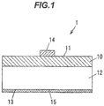
- FIG.1 is a vertical cross-sectional view showing a high-withstand voltage Schottky barrier diode 1 in an embodiment.
- the high-withstand voltage Schottky barrier diode 1 is a vertical Schottky barrier diode and has a first layer 10, a second layer 12 laminated on the first layer 10, an anode electrode 14 formed on the first layer 10, and a cathode electrode 15 formed on the second layer 12.
- the first layer 10 is formed of a Ga 2 O 3 -based single crystal containing a Group IV element, such as Si or Sn, as a donor.
- a Group IV element such as Si or Sn
- Sn is known to tend to segregate, and use of Sn as a donor may cause poor in-plane uniformity of electrical characteristics of the first layer 10 and a decrease in production yield. Therefore, use of Si as a donor is more preferable.
- An effective donor concentration (N d -N a ) of the first layer 10 is not less than 1x10 13 and not more than 6.0x10 17 cm -3 , preferably not more than 2.0x10 16 cm -3 , and more preferably not more than 1.4x10 16 cm -3 .
- N d -N a here is a difference between a donor concentration N d and an acceptor concentration Na, and corresponds to a concentration of donor which effectively functions.
- the high withstand voltage Schottky barrier diode 1 can have a withstand voltage (breakdown voltage) of not less than 16V, not less than 310V, not less than 360V and not less than 440V, respectively.
- the withstand voltage as defined here is a magnitude of applied voltage at which a density of reverse leakage current flowing between the anode electrode 14 and the cathode electrode 15 in the high withstand voltage Schottky barrier diode 1 reaches 10 -3 A/cm 2 .
- a higher withstand voltage can be obtained by additionally providing an electric field concentration relaxation structure, such as a field plate structure in which an insulating film is formed at an edge portion of the anode electrode 14 on the surface of the first layer 10, or a guard ring structure in which acceptor ions are implanted in the first layer 10 and at the edge and surrounding portions of the anode electrode 14 on the surface of the first layer 10.
- an electric field concentration relaxation structure such as a field plate structure in which an insulating film is formed at an edge portion of the anode electrode 14 on the surface of the first layer 10, or a guard ring structure in which acceptor ions are implanted in the first layer 10 and at the edge and surrounding portions of the anode electrode 14 on the surface of the first layer 10.
- the first layer 10 also contains Cl at a concentration of not more than 5x10 16 cm -3 .
- Cl-containing gas is not used to form a Ga 2 O 3 -based single crystal film when using a method other than the HVPE method, and the Ga 2 O 3 -based single crystal film does not contain Cl, or at least does not contain 1x10 16 cm -3 or more of Cl.
- the thickness of the first layer 10 is preferably not less than 30 nm so that the high withstand voltage Schottky barrier diode 1 can have sufficient withstand voltage characteristics.
- the withstand voltage of the high withstand voltage Schottky barrier diode 1 depends on the thickness and N d -N a of the first layer 10. For example, when N d -N a of the first layer 10 is 6.0x10 17 cm -3 , the withstand voltage of 21 V can be obtained as long as the thickness of the first layer 10 is not less than 30 nm.
- the upper limit of the thickness of the first layer 10 is not specifically limited. However, since electrical resistance in the thickness direction increases with an increase in thickness, the first layer 10 is preferably as thin as possible within the range in which the required withstand voltage characteristics can be obtained.
- the Ga 2 O 3 -based single crystal here means a Ga 2 O 3 single crystal or is a Ga 2 O 3 single crystal doped with an element such as Al or In, and may be, e.g., a (Ga x Al y In (1-x-y) ) 2 O 3 ( 0 ⁇ x ⁇ 1 , 0 ⁇ y ⁇ 1 , 0 ⁇ x+y ⁇ 1 ) single crystal which is a Ga 2 O 3 single crystal doped with A1 and In.
- the band gap is widened by adding Al and is narrowed by adding In.
- Such Ga 2 O 3 single crystal has, e.g., a ⁇ -crystal structure.
- the second layer 12 is formed of a second Ga 2 O 3 -based single crystal containing a Group IV element, such as Si or Sn, as a donor.
- N d -N a of the second layer 12 is higher than that of the first layer 10 and is, e.g., not less than 1x10 18 and not more than 1.0x10 20 cm -3 .
- the thickness of the second layer 12 is, e.g., 50 to 1000 ⁇ m.
- the plane orientations of the principal surfaces of the first layer 10 and the second layer 12 are not specifically limited and are, e.g., (001), (010), (110), (210), (310), (610), (910), (101), (102), (201), (401), (-101), (-201), (-102) or (-401), in view of crystal growth rate, etc.
- the anode electrode 14 is formed on a surface 11 of the first layer 10, which is a surface on the opposite side to the second layer 12, and is in Schottky contact with the first layer 10.
- the anode electrode 14 is formed of a metal such as Pt or Ni.
- the anode electrode 14 may have a multilayer structure formed by laminating different metal films, e.g., Pt/Au or Pt/Al.
- the cathode electrode 15 is formed on a surface 13 of the second layer 12, which is a surface on the opposite side to the first layer 10, and is in ohmic contact with the second layer 12.
- the cathode electrode 15 is formed of a metal such as Ti.
- the cathode electrode 15 may have a multilayer structure formed by laminating different metal films, e.g., Ti/Au or Ti/Al.
- a layer constituting the cathode electrode 15 and in contact with the second layer 12 is preferably formed of Ti so that the cathode electrode 15 can be reliably in ohmic contact with the second layer 12.
- the second layer 12 is a Ga 2 O 3 -based substrate and the first layer 10 is a Ga 2 O 3 -based single crystal film epitaxially grown on the second layer 12.
- the second layer 12 is not formed by the HVPE method and thus practically does not contain Cl.
- the high withstand voltage Schottky barrier diode 1 can have another structure in which both the first layer 10 and the second layer 12 are epitaxial films.
- the first layer 10 and the second layer 12 are, e.g., epitaxially grown on a base substrate formed of a Ga 2 O 3 -based single crystal and then separated from the base substrate.
- the thickness of the second layer 12 is, e.g., 0.1 to 50 ⁇ m.
- a Ga 2 O 3 -based single crystal film as the first layer 10 is epitaxially grown on a Ga 2 O 3 -based substrate as the second layer 12.
- a bulk crystal of a Ga 2 O 3 -based single crystal grown by a melt-growth technique such as the FZ (Floating Zone) method or the EFG (Edge Defined Film Fed Growth) method is sliced and the surface thereof is then polished, thereby forming a Ga 2 O 3 -based substrate as the second layer 12.
- a Ga 2 O 3 -based single crystal film as the first layer 10 is epitaxially grown on the Ga 2 O 3 -based substrate by the HVPE (Halide Vapor Phase Epitaxy) method.
- HVPE Hydrode Vapor Phase Epitaxy
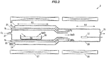
- FIG.2 is a vertical cross-sectional view showing a vapor phase deposition system 2 designed to use the HVPE method.
- the vapor phase deposition system 2 has a reaction chamber 20 having a first gas introducing port 21, a second gas introducing port 22, a third gas introducing port 23, a fourth gas introducing port 24 and an exhaust port 25, and a first heating means 27 and a second heating means 28 which are placed to surround the reaction chamber 20 to heat predetermined regions in the reaction chamber 20.
- the growth rate when using the HVPE method is higher than that in the MBE method, etc.
- in-plane distribution of film thickness is highly uniform and it is possible to grow a large-diameter film. Therefore, it is suitable for mass production of crystal.
- the reaction chamber 20 has a source reaction region R 1 in which a reaction container 26 containing a Ga source is placed and a gallium source gas is produced, and a crystal growth region R 2 in which the Ga 2 O 3 -based substrate is placed and the Ga 2 O 3 -based single crystal film is grown thereon.
- the reaction chamber 20 is formed of, e.g., quartz glass.
- reaction container 26 is formed of, e.g., quartz glass and the Ga source contained in the reaction container 26 is metal gallium.
- the first heating means 27 and the second heating means 28 are capable of respectively heating the source reaction region R 1 and the crystal growth region R 2 of the reaction chamber 20.
- the first heating means 27 and the second heating means 28 are, e.g., resistive heaters or radiation heaters.
- the first gas introducing port 21 is a port for introducing a Cl-containing gas (Ch gas or HCl gas) into the source reaction region R 1 of the reaction chamber 20 using an inert carrier gas (N 2 gas, Ar gas or He gas).
- the second gas introducing port 22 is a port for introducing an oxygen-containing gas (O 2 gas or H 2 O gas, etc.) as an oxygen source gas into the crystal growth region R 2 of the reaction chamber 20 using an inert carrier gas (N 2 gas, Ar gas or He gas).
- the third gas introducing port 23 is a port for introducing an inert carrier gas (N 2 gas, Ar gas or He gas) into the crystal growth region R 2 of the reaction chamber 20.
- the fourth gas introducing port 24 is a port for introducing a source gas of dopant to be added to the Ga 2 O 3 -based single crystal film, such as Si (e.g., silicon tetrachloride, etc.), into the crystal growth region R 2 of the reaction chamber 20 using an inert carrier gas (N 2 gas, Ar gas or He gas).
- a source gas of dopant such as Si (e.g., silicon tetrachloride, etc.)
- Ga 2 O 3 -based single crystal film it is possible to use a technique of growing Ga 2 O 3 -based single crystal film disclosed by Japanese patent application No. 2014-088589 .
- a process of growing the Ga 2 O 3 -based single crystal film in the present embodiment will be described below as an example.
- the source reaction region R 1 of the reaction chamber 20 is heated by the first heating means 27 and an atmosphere temperature in the source reaction region R 1 is then maintained at a predetermined temperature.
- a Cl-containing gas introduced through the first gas introducing port 21 using a carrier gas is reacted with the metal gallium in the reaction container 26 at the above-mentioned atmosphere temperature, thereby producing a gallium chloride gas.
- the atmosphere temperature in the source reaction region R1 here is preferably a temperature at which GaCl gas has the highest partial pressure among component gases of the gallium chloride gas produced by the reaction of the metal gallium in the reaction container 26 with the Cl-containing gas.
- the gallium chloride gas here contains GaCl gas, GaCl 2 gas, GaCl 3 gas and (GaCl 3 ) 2 gas, etc.
- the temperature at which a driving force for growth of Ga 2 O 3 crystal is maintained is the highest with the GaCl gas among the gases contained in the gallium chloride gas. Growth at a high temperature is effective to obtain a high-quality Ga 2 O 3 crystal with high purity. Therefore, for growing the Ga 2 O 3 -based single crystal film, it is preferable to produce a gallium chloride gas in which a partial pressure of GaCl gas having a high driving force for growth at a high temperature is high.
- the metal gallium in the reaction container 26 be reacted with the Cl-containing gas in a state that the atmosphere temperature in the source reaction region R 1 is maintained at not less than 300 °C by using the first heating means 27.
- the partial pressure ratio of the GaCl gas is predominantly high (the equilibrium partial pressure of the GaCl gas is four orders of magnitude greater than the GaCl 2 gas and is eight orders of magnitude greater than the GaCl 3 gas) and the gases other than GaCl gas hardly contribute to the growth of Ga 2 O 3 crystal.
- the metal gallium in the reaction container 26 be reacted with the Cl-containing gas in a state that the atmosphere temperature in the source reaction region R 1 is maintained at not more than 1000°C.
- the gallium chloride gas produced in the source reaction region R 1 is mixed with the oxygen-containing gas introduced through the second gas introducing port 22 and the dopant source gas such as Si introduced through the fourth gas introducing port 24, the Ga 2 O 3 -based substrate is then exposed to the mixed gas, and the Ga 2 O 3 -based single crystal film containing the dopant is thereby epitaxially grown on the Ga 2 O 3 -based substrate.
- pressure in the crystal growth region R 2 is maintained at, e.g., 1 atm.
- the dopant source gas used here is preferably a chloride-based gas to prevent other unintentional impurities from being mixed.
- a chloride-based gas such as SiCl 4 , GeCl 4 , SnCl 4 or PbCl 2 , respectively, is used.
- the chloride-based gas is not limited to a compound of an element with only chlorine, and may be, e.g., a silane-based gas such as SiHCl 3 .
- the dopant such as Si is doped during growth of the Ga 2 O 3 -based single crystal (in-situ doping).
- an O 2 gas not containing hydrogen be used as the oxygen-containing gas.
- the GaCl gas is consumed in growth of Ga 2 O 3 crystal and the Ga 2 O 3 crystal grows efficiently.
- the equilibrium partial pressure of the GaCl gas sharply falls when a ratio of the supplied partial pressure of the O 2 gas to the supplied partial pressure of the GaCl gas (the O 2 /GaCl supplied partial pressure ratio) is not less than 0.5. Therefore, to efficiently grow the Ga 2 O 3 -based single crystal film, the Ga 2 O 3 -based single crystal film is preferably grown in a state that the O 2 /GaCl supplied partial pressure ratio in the crystal growth region R 2 is not less than 0.5.
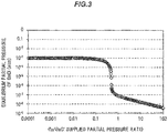
- FIG.3 is a graph which is obtained by thermal equilibrium calculation and shows a relation between an equilibrium partial pressure of GaCl and an O 2 /GaCl supplied partial pressure ratio when the atmosphere temperature during Ga 2 O 3 crystal growth is 1000 °C. It is calculated using the supplied partial pressure value of the GaCl gas fixed to 1x10 -3 atm, a furnace pressure of 1 atom adjusted by using, e.g., an inert gas such as N 2 as a carrier gas, and various values of the O 2 gas supplied partial pressure.
- an inert gas such as N 2 as a carrier gas
- the horizontal axis indicates the O 2 /GaCl supplied partial pressure ratio and the vertical axis indicates an equilibrium partial pressure (atm) of GaCl gas. It is shown that the smaller the equilibrium partial pressure of the GaCl gas, the more the GaCl gas is consumed for growth of Ga 2 O 3 crystal, i.e., the Ga 2 O 3 crystal grows efficiently.
- FIG.3 shows that the equilibrium partial pressure of the GaCl gas sharply falls at the O 2 /GaCl supplied partial pressure ratio of not less than 0.5.
- a growth temperature of not less than 900 °C is required to grow the Ga 2 O 3 -based single crystal film.
- a single crystal may not be obtained at less than 900 °C.
- Undoped Ga 2 O 3 -based single crystal films grown by the HVPE method have a residual carrier concentration of not more than 1x10 13 cm -3 , as disclosed by Japanese patent application No. 2014-088589 . Therefore, N d -N a of the Ga 2 O 3 -based single crystal film can be changed in the range of not less than 1x10 13 cm -3 by changing the Group IV element doping concentration.
- the surface of the Ga 2 O 3 -based single crystal film is flattened by CMP (Chemical Mechanical Polishing).
- CMP Chemical Mechanical Polishing
- surface roughness (RMS) of not more than 1 nm is obtained when polished 2 ⁇ m in a depth direction. Reducing the surface roughness by the flattening process prevents local electric field concentration when reverse voltage is applied to the anode electrode, resulting in improvement in withstand voltage of the Schottky barrier diode.
- RMS surface roughness
- the polishing amount in the depth direction is not specifically limited, at least 1 ⁇ m or more should be polished for such purpose.
- the anode electrode 14 and the cathode electrode 15 are formed respectively on the surface 11 of the Ga 2 O 3 -based single crystal film as the first layer 10 and the surface 13 of the Ga 2 O 3 -based substrate as the second layer 12.
- the second layer 12 is an epitaxial layer
- the second layer 12 is formed on a base substrate by the HVPE method in the same manner as the method of forming the first layer 10 described above.
- This base substrate is removed from the second layer 12 before forming the cathode electrode 15.
- the first layer 10, or the first layer 10 and the second layer 12, containing a desired concentration of donor and having high uniformity of donor concentration distribution can be obtained by adding a dopant while growing the Ga 2 O 3 -based single crystal using the HVPE method.
- a dopant while growing the Ga 2 O 3 -based single crystal using the HVPE method.
- Example 2 O 3 single crystal film as the first layer 10 was epitaxially grown on a Ga 2 O 3 substrate as the second layer 12 having a ( 001 )-oriented principal surface.
- a Sn-doped Ga 2 O 3 single crystal grown by the EFG method was sliced and polished, thereby forming plural Ga 2 O 3 substrates.
- N d -N a of the Ga 2 O 3 substrates was about 2.5x10 18 cm -3 .
- the thickness of the Ga 2 O 3 substrates was about 650 ⁇ m.
- Ga 2 O 3 single crystal films having a thickness of about 10 ⁇ m was grown on each of the plural Ga 2 O 3 substrates by the HVPE method.
- the Ga 2 O 3 single crystal films respectively had a Si concentration of about 2.0x10 15 cm -3 , 1.4x10 16 cm -3 , 2.0x10 16 cm -3 , 1.0x10 17 cm -3 , 1.5x10 17 cm -3 , 2.9x10 17 cm -3 and 6.0x10 17 cm -3 .
- each Ga 2 O 3 single crystal film was treated by CMP from the surface to a depth of about 2 to 3 ⁇ m and was thereby flattened.
- the surface of the Ga 2 O 3 substrate on the opposite side to the Ga 2 O 3 single crystal film was also flattened by grinding, polishing and CMP from the surface to a depth of about 50 ⁇ m.
- a cathode electrode composed of a lamination of a 20 nm-thick Ti film and a 230 nm-thick Au film was formed on the Ga 2 O 3 substrate by vapor deposition.
- a circular anode electrode composed of a lamination of a 15 nm-thick Pt film, a 5 nm-thick Ti film and a 250 nm-thick Au film was formed the Ga 2 O 3 single crystal film.
- the diameter of the anode electrode was 200 ⁇ m for current-voltage (I-V) measurement and 400 ⁇ m for capacitance-voltage (C-V) measurement.
- FIG.4 is a graph showing N d -N a profiles in a depth direction of Ga 2 O 3 single crystal films of seven types of Schottky barrier diodes, based on calculation using C-V measurement results.
- the Ga 2 O 3 single crystal films of the seven Schottky barrier diodes respectively had N d -N a of about 2.0x10 15 cm -3 , 1.4x10 16 cm -3 , 2.0x10 16 cm -3 , 1.0x10 17 cm -3 , 1.5x10 17 cm -3 , 2.9x10 17 cm -3 and 6.0x10 17 cm -3 .
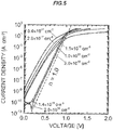
- FIG.5 is a graph showing forward characteristics of the seven types of Schottky barrier diodes.
- An inclination of the dotted line in FIG.5 represents an inclination of I-V curve at lower voltage than the rising voltage when the ideality factor n of Schottky barrier diode is 1 (ideal value).
- the Schottky ideality factor was about 1.01 to 1.03 and an ideal Schottky contact was formed.
- the ideality factor was about 1.2 due to leakage current.
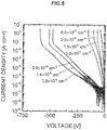
- FIG.6 is a graph showing reverse characteristics of the seven types of Schottky barrier diodes. With the decrease in donor concentration, reverse leakage current decreased and withstand voltage increased. The withstand voltage in each profile is the magnitude of voltage at the current density of 10 -3 A/cm 2 .
- the withstand voltage of the Schottky barrier diode having N d -N a of 2.0x10 15 cm -3 was about 440V
- the withstand voltage of the Schottky barrier diode having N d -N a of 1.4x10 16 cm -3 was about 360V
- the withstand voltage of the Schottky barrier diode having N d -N a of 2.0x10 16 cm -3 was about 310V
- the withstand voltage of the Schottky barrier diode having N d -N a of 1.0x10 17 cm -1 was about 74V
- the withstand voltage of the Schottky barrier diode having N d -N a of 1.5x10 17 cm -3 was about 46V
- the withstand voltage of the Schottky barrier diode having N d -N a of 2.9x10 17 cm -3 was about 36V
- Ga 2 O 3 substrates having a ( 001 )-oriented principal surface were used as the Ga 2 O 3 -based substrates in the evaluation, similar evaluation results are obtained also when another Ga 2 O 3 -based substrate is used instead of the Ga 2 O 3 substrate or the plane orientation of the principal surface is different. In addition, similar evaluation results are obtained also when another Ga 2 O 3 -based single crystal film is formed instead of the Ga 2 O 3 single crystal film.
- N d -N a of the Ga 2 O 3 single crystal film was 2.0x10 15 to 6.0x10 17 cm -3 in the evaluation, higher withstand voltage is obtained when using a Ga 2 O 3 single crystal film with lower N d -N a .
- Ga 2 O 3 -based high withstand voltage Schottky barrier diode having excellent withstand voltage characteristics.
Landscapes
- Chemical & Material Sciences (AREA)
- Engineering & Computer Science (AREA)
- Materials Engineering (AREA)
- Metallurgy (AREA)
- Organic Chemistry (AREA)
- Crystallography & Structural Chemistry (AREA)
- General Chemical & Material Sciences (AREA)
- Chemical Kinetics & Catalysis (AREA)
- Inorganic Chemistry (AREA)
- Mechanical Engineering (AREA)
- Electrochemistry (AREA)
- Electrodes Of Semiconductors (AREA)
- Crystals, And After-Treatments Of Crystals (AREA)
- Recrystallisation Techniques (AREA)
- Chemical Vapour Deposition (AREA)
Abstract
Description
- The invention relates to a high-withstand voltage Schottky barrier diode.
- Known as a method for doping a Ga2O3-based single crystal are a method in which a dopant is added during crystal growth by the MBE (Molecular Beam Epitaxy) method or the EFG (Edge-defined Film-fed Growth) method (see, e.g.,
PTLs 1 and 2) and a method in which a dopant is added to a grown Ga2O3-based single crystal by ion implantation (see e.g. PTL 3). Also, a Schottky barrier diode formed of a Ga2O3-based compound semiconductor (e.g. PTL 4) is known. -
- [PTL 1] JP-A-2013-056803
- [PTL 2] JP-A-2013-082587
- [PTL 3] JP-A-2013-058637
- [PTL 4] JP-A-2013-102081
- When using the MBE method, however, impurities are likely to segregate during epitaxial crystal growth and uniformity of dopant concentration distribution in depth and in-plane directions is poor.
- Also, in the EFG method, since a raw material contains an impurity at a concentration of about 1x1017 cm-3, doping with a lower concentration is not possible.
- Also, in the ion implantation, implantation depth of the impurity ion is limited to about 1 µm. Furthermore, since the ion beam damages the crystal, the crystallinity deteriorates.
- Thus, by the prior arts, it is not possible to form a Ga2O3-based single crystal containing a desired concentration of donor as well as having high uniformity of donor concentration distribution, and it is difficult to manufacture a Ga2O3-based Schottky barrier diode with excellent withstand voltage characteristics.
- Thus, it is one of objects of the invention to provide a Ga2O3-based high-withstand voltage Schottky barrier diode that is excellent in withstand voltage characteristics.
- For completing the abovementioned object, according to an embodiment of the invention, a high-withstand voltage Schottky barrier diode defined by [1] to [6] below is provided.
- [1] A high withstand voltage Schottky barrier diode, comprising: a first layer that comprises a first Ga2O3-based single crystal including a first Group IV element and Cl at a concentration of not more than 5x1016 cm-3 and has an effective donor concentration of not less than 1x10¹³ and not more than 6.0x1017 cm-3; a second layer that comprises a second Ga2O3-based single crystal including a second Group IV element and that has a higher effective donor concentration than the first layer and is laminated on the first layer; an anode electrode formed on the first layer; and a cathode electrode formed on the second layer.
- [2] The high withstand voltage Schottky barrier diode defined by [1], wherein the effective donor concentration of the first layer is not more than 2.0x1016 cm-3.
- [3] The high withstand voltage Schottky barrier diode defined by [2], wherein the effective donor concentration of the first layer is not more than 1.4x1016 cm-3.
- [4] The high withstand voltage Schottky barrier diode defined by any one of [1] to [3], wherein the first Group IV element comprises Si.
- [5] The high withstand voltage Schottky barrier diode defined by any one of [1] to [3], wherein the first Ga2O3-based single crystal comprises a Ga2O3 single crystal.
- [6] The high withstand voltage Schottky barrier diode defined by any one of [1] to [3], wherein a layer of the cathode electrode contacts with the second layer and comprises Ti.
- According to the invention, it is possible to provide a Ga2O3-based high-withstand voltage Schottky barrier diode that is excellent in withstand voltage characteristics.
-
-
FIG.1 is a vertical cross-sectional view showing a high-withstand voltageSchottky barrier diode 1 in an embodiment. -
FIG.2 is a vertical cross-sectional view showing a vapor phase deposition system designed to use the HVPE method. -
FIG.3 is a graph which is obtained by thermal equilibrium calculation and shows a relation between equilibrium partial pressure of GaCl and an O2/GaCl supplied partial pressure ratio when the atmosphere temperature during Ga2O3 crystal growth is 1000°C. -
FIG.4 is a graph showing Nd-Na profiles in a depth direction of Ga2O3 single crystal films of seven types of Schottky barrier diodes, based on calculation using C-V measurement results. -
FIG.5 is a graph showing forward characteristics of the seven types of Schottky barrier diodes. -
FIG.6 is a graph showing reverse characteristics of the seven types of Schottky barrier diodes. -
FIG.1 is a vertical cross-sectional view showing a high-withstand voltageSchottky barrier diode 1 in an embodiment. The high-withstand voltage Schottkybarrier diode 1 is a vertical Schottky barrier diode and has afirst layer 10, asecond layer 12 laminated on thefirst layer 10, ananode electrode 14 formed on thefirst layer 10, and acathode electrode 15 formed on thesecond layer 12. - The
first layer 10 is formed of a Ga2O3-based single crystal containing a Group IV element, such as Si or Sn, as a donor. In this regard, Sn is known to tend to segregate, and use of Sn as a donor may cause poor in-plane uniformity of electrical characteristics of thefirst layer 10 and a decrease in production yield. Therefore, use of Si as a donor is more preferable. An effective donor concentration (Nd-Na) of thefirst layer 10 is not less than 1x10¹³ and not more than 6.0x1017 cm-3, preferably not more than 2.0x1016 cm-3, and more preferably not more than 1.4x1016 cm-3. Nd-Na here is a difference between a donor concentration Nd and an acceptor concentration Na, and corresponds to a concentration of donor which effectively functions. - When Nd-Na of the
first layer 10 is not more than 6.0x1017 cm-3, not more than 2.0x1016 cm-3, not more than 1.4x1016 cm-3 and not more than 2.0x1015 cm-3, the high withstand voltageSchottky barrier diode 1 can have a withstand voltage (breakdown voltage) of not less than 16V, not less than 310V, not less than 360V and not less than 440V, respectively. Based on general device evaluation criteria, the withstand voltage as defined here is a magnitude of applied voltage at which a density of reverse leakage current flowing between theanode electrode 14 and thecathode electrode 15 in the high withstand voltageSchottky barrier diode 1 reaches 10-3 A/cm2. - A higher withstand voltage can be obtained by additionally providing an electric field concentration relaxation structure, such as a field plate structure in which an insulating film is formed at an edge portion of the
anode electrode 14 on the surface of thefirst layer 10, or a guard ring structure in which acceptor ions are implanted in thefirst layer 10 and at the edge and surrounding portions of theanode electrode 14 on the surface of thefirst layer 10. - The
first layer 10 also contains Cl at a concentration of not more than 5x1016 cm-3. This results from that the Ga2O3-based single crystal film is formed by the HVPE method using Cl-containing gas. Generally, Cl-containing gas is not used to form a Ga2O3-based single crystal film when using a method other than the HVPE method, and the Ga2O3-based single crystal film does not contain Cl, or at least does not contain 1x1016 cm-3 or more of Cl. - The thickness of the
first layer 10 is preferably not less than 30 nm so that the high withstand voltageSchottky barrier diode 1 can have sufficient withstand voltage characteristics. The withstand voltage of the high withstand voltageSchottky barrier diode 1 depends on the thickness and Nd-Na of thefirst layer 10. For example, when Nd-Na of thefirst layer 10 is 6.0x1017 cm-3, the withstand voltage of 21V can be obtained as long as the thickness of thefirst layer 10 is not less than 30 nm. The upper limit of the thickness of thefirst layer 10 is not specifically limited. However, since electrical resistance in the thickness direction increases with an increase in thickness, thefirst layer 10 is preferably as thin as possible within the range in which the required withstand voltage characteristics can be obtained. - The Ga2O3-based single crystal here means a Ga2O3 single crystal or is a Ga2O3 single crystal doped with an element such as Al or In, and may be, e.g., a (GaxAlyIn(1-x-y))2O3 (0<x≤1, 0≤y<1, 0<x+y≤1) single crystal which is a Ga2O3 single crystal doped with A1 and In. The band gap is widened by adding Al and is narrowed by adding In. Such Ga2O3 single crystal has, e.g., a β-crystal structure.
- The
second layer 12 is formed of a second Ga2O3-based single crystal containing a Group IV element, such as Si or Sn, as a donor. Nd-Na of thesecond layer 12 is higher than that of thefirst layer 10 and is, e.g., not less than 1x10¹⁸ and not more than 1.0x1020 cm-3. The thickness of thesecond layer 12 is, e.g., 50 to 1000 µm. - Since withstand voltage of the high withstand voltage Schottky
barrier diode 1 hardly depends on plane orientations of principal surfaces of thefirst layer 10 and thesecond layer 12, the plane orientations of the principal surfaces of thefirst layer 10 and thesecond layer 12 are not specifically limited and are, e.g., (001), (010), (110), (210), (310), (610), (910), (101), (102), (201), (401), (-101), (-201), (-102) or (-401), in view of crystal growth rate, etc. - The
anode electrode 14 is formed on asurface 11 of thefirst layer 10, which is a surface on the opposite side to thesecond layer 12, and is in Schottky contact with thefirst layer 10. - The
anode electrode 14 is formed of a metal such as Pt or Ni. Theanode electrode 14 may have a multilayer structure formed by laminating different metal films, e.g., Pt/Au or Pt/Al. - The
cathode electrode 15 is formed on asurface 13 of thesecond layer 12, which is a surface on the opposite side to thefirst layer 10, and is in ohmic contact with thesecond layer 12. - The
cathode electrode 15 is formed of a metal such as Ti. Thecathode electrode 15 may have a multilayer structure formed by laminating different metal films, e.g., Ti/Au or Ti/Al. A layer constituting thecathode electrode 15 and in contact with thesecond layer 12 is preferably formed of Ti so that thecathode electrode 15 can be reliably in ohmic contact with thesecond layer 12. - In the high withstand voltage
Schottky barrier diode 1, when voltage in a forward direction (electric potential is positive on theanode electrode 14 side) is applied between theanode electrode 14 and thecathode electrode 15, height of the energy barrier at an interface between theanode electrode 14 and thefirst layer 10 decreases as viewed from thefirst layer 10 and an electric current flows from theanode electrode 14 to thecathode electrode 15. On the other hand, when voltage in a reverse direction (electric potential is negative on theanode electrode 14 side) is applied between theanode electrode 14 and thecathode electrode 15, an electric current does not flow due to the Schottky barrier. - In the typical structure of the high withstand voltage
Schottky barrier diode 1, thesecond layer 12 is a Ga2O3-based substrate and thefirst layer 10 is a Ga2O3-based single crystal film epitaxially grown on thesecond layer 12. When thesecond layer 12 is a Ga2O3-based substrate, thesecond layer 12 is not formed by the HVPE method and thus practically does not contain Cl. - As an alternative, the high withstand voltage
Schottky barrier diode 1 can have another structure in which both thefirst layer 10 and thesecond layer 12 are epitaxial films. In this case, thefirst layer 10 and thesecond layer 12 are, e.g., epitaxially grown on a base substrate formed of a Ga2O3-based single crystal and then separated from the base substrate. In this case, the thickness of thesecond layer 12 is, e.g., 0.1 to 50 µm. - An example of a method for manufacturing the high withstand voltage
Schottky barrier diode 1 will be described below. In this example, a Ga2O3-based single crystal film as thefirst layer 10 is epitaxially grown on a Ga2O3-based substrate as thesecond layer 12. - Firstly, a bulk crystal of a Ga2O3-based single crystal grown by a melt-growth technique such as the FZ (Floating Zone) method or the EFG (Edge Defined Film Fed Growth) method is sliced and the surface thereof is then polished, thereby forming a Ga2O3-based substrate as the
second layer 12. - Next, a Ga2O3-based single crystal film as the
first layer 10 is epitaxially grown on the Ga2O3-based substrate by the HVPE (Halide Vapor Phase Epitaxy) method. -
FIG.2 is a vertical cross-sectional view showing a vaporphase deposition system 2 designed to use the HVPE method. The vaporphase deposition system 2 has areaction chamber 20 having a firstgas introducing port 21, a secondgas introducing port 22, a thirdgas introducing port 23, a fourth gas introducing port 24 and anexhaust port 25, and a first heating means 27 and a second heating means 28 which are placed to surround thereaction chamber 20 to heat predetermined regions in thereaction chamber 20. - The growth rate when using the HVPE method is higher than that in the MBE method, etc. In addition, in-plane distribution of film thickness is highly uniform and it is possible to grow a large-diameter film. Therefore, it is suitable for mass production of crystal.
- The
reaction chamber 20 has a source reaction region R1 in which areaction container 26 containing a Ga source is placed and a gallium source gas is produced, and a crystal growth region R2 in which the Ga2O3-based substrate is placed and the Ga2O3-based single crystal film is grown thereon. Thereaction chamber 20 is formed of, e.g., quartz glass. - Here, the
reaction container 26 is formed of, e.g., quartz glass and the Ga source contained in thereaction container 26 is metal gallium. - The first heating means 27 and the second heating means 28 are capable of respectively heating the source reaction region R1 and the crystal growth region R2 of the
reaction chamber 20. The first heating means 27 and the second heating means 28 are, e.g., resistive heaters or radiation heaters. - The first
gas introducing port 21 is a port for introducing a Cl-containing gas (Ch gas or HCl gas) into the source reaction region R1 of thereaction chamber 20 using an inert carrier gas (N2 gas, Ar gas or He gas). The secondgas introducing port 22 is a port for introducing an oxygen-containing gas (O2 gas or H2O gas, etc.) as an oxygen source gas into the crystal growth region R2 of thereaction chamber 20 using an inert carrier gas (N2 gas, Ar gas or He gas). The thirdgas introducing port 23 is a port for introducing an inert carrier gas (N2 gas, Ar gas or He gas) into the crystal growth region R2 of thereaction chamber 20. The fourth gas introducing port 24 is a port for introducing a source gas of dopant to be added to the Ga2O3-based single crystal film, such as Si (e.g., silicon tetrachloride, etc.), into the crystal growth region R2 of thereaction chamber 20 using an inert carrier gas (N2 gas, Ar gas or He gas). - To grow the Ga2O3-based single crystal film, it is possible to use a technique of growing Ga2O3-based single crystal film disclosed by Japanese patent application No.
2014-088589 - Firstly, the source reaction region R1 of the
reaction chamber 20 is heated by the first heating means 27 and an atmosphere temperature in the source reaction region R1 is then maintained at a predetermined temperature. - Next, in the source reaction region R1, a Cl-containing gas introduced through the first
gas introducing port 21 using a carrier gas is reacted with the metal gallium in thereaction container 26 at the above-mentioned atmosphere temperature, thereby producing a gallium chloride gas. - The atmosphere temperature in the source reaction region R1 here is preferably a temperature at which GaCl gas has the highest partial pressure among component gases of the gallium chloride gas produced by the reaction of the metal gallium in the
reaction container 26 with the Cl-containing gas. The gallium chloride gas here contains GaCl gas, GaCl2 gas, GaCl3 gas and (GaCl3)2 gas, etc. - The temperature at which a driving force for growth of Ga2O3 crystal is maintained is the highest with the GaCl gas among the gases contained in the gallium chloride gas. Growth at a high temperature is effective to obtain a high-quality Ga2O3 crystal with high purity. Therefore, for growing the Ga2O3-based single crystal film, it is preferable to produce a gallium chloride gas in which a partial pressure of GaCl gas having a high driving force for growth at a high temperature is high.
- It is possible to increase a partial pressure ratio of the GaCl gas in the gallium chloride gas by reacting the metal gallium with the Cl-containing gas at an atmosphere temperature of about not less than 300°C. Therefore, it is preferable that the metal gallium in the
reaction container 26 be reacted with the Cl-containing gas in a state that the atmosphere temperature in the source reaction region R1 is maintained at not less than 300°C by using the first heating means 27. - At the atmosphere temperature of, e.g., 850°C, the partial pressure ratio of the GaCl gas is predominantly high (the equilibrium partial pressure of the GaCl gas is four orders of magnitude greater than the GaCl2 gas and is eight orders of magnitude greater than the GaCl3 gas) and the gases other than GaCl gas hardly contribute to the growth of Ga2O3 crystal.
- Also, considering the lifetime of the first heating means 27 and heat resistance of the
reaction chamber 20 formed of quartz glass, etc., it is preferable that the metal gallium in thereaction container 26 be reacted with the Cl-containing gas in a state that the atmosphere temperature in the source reaction region R1 is maintained at not more than 1000°C. - In addition, if hydrogen is contained in an atmosphere for growing the Ga2O3-based single crystal film, surface flatness and a driving force for growth of the Ga2O3-based single crystal film decrease. Therefore, it is preferable that a Cl2 gas not containing hydrogen be used as the Cl-containing gas.
- Next, in the crystal growth region R2, the gallium chloride gas produced in the source reaction region R1 is mixed with the oxygen-containing gas introduced through the second
gas introducing port 22 and the dopant source gas such as Si introduced through the fourth gas introducing port 24, the Ga2O3-based substrate is then exposed to the mixed gas, and the Ga2O3-based single crystal film containing the dopant is thereby epitaxially grown on the Ga2O3-based substrate. At this time, in a furnace housing thereaction chamber 20, pressure in the crystal growth region R2 is maintained at, e.g., 1 atm. - The dopant source gas used here is preferably a chloride-based gas to prevent other unintentional impurities from being mixed. For example, when Si, Ge, Sn or Pb is used as a dopant, a chloride-based gas such as SiCl4, GeCl4, SnCl4 or PbCl2, respectively, is used. Here, the chloride-based gas is not limited to a compound of an element with only chlorine, and may be, e.g., a silane-based gas such as SiHCl3.
- The dopant such as Si is doped during growth of the Ga2O3-based single crystal (in-situ doping).
- If hydrogen is contained in an atmosphere for growing the Ga2O3-based single crystal film, surface flatness and a driving force for growth of the Ga2O3-based single crystal film decrease. Therefore, it is preferable that an O2 gas not containing hydrogen be used as the oxygen-containing gas.
- Also, according as the equilibrium partial pressure of the GaCl gas decreases, the GaCl gas is consumed in growth of Ga2O3 crystal and the Ga2O3 crystal grows efficiently. For example, the equilibrium partial pressure of the GaCl gas sharply falls when a ratio of the supplied partial pressure of the O2 gas to the supplied partial pressure of the GaCl gas (the O2/GaCl supplied partial pressure ratio) is not less than 0.5. Therefore, to efficiently grow the Ga2O3-based single crystal film, the Ga2O3-based single crystal film is preferably grown in a state that the O2/GaCl supplied partial pressure ratio in the crystal growth region R2 is not less than 0.5.
-
FIG.3 is a graph which is obtained by thermal equilibrium calculation and shows a relation between an equilibrium partial pressure of GaCl and an O2/GaCl supplied partial pressure ratio when the atmosphere temperature during Ga2O3 crystal growth is 1000°C. It is calculated using the supplied partial pressure value of the GaCl gas fixed to 1x10⁻³ atm, a furnace pressure of 1 atom adjusted by using, e.g., an inert gas such as N2 as a carrier gas, and various values of the O2 gas supplied partial pressure. - In
FIG.3 , the horizontal axis indicates the O2/GaCl supplied partial pressure ratio and the vertical axis indicates an equilibrium partial pressure (atm) of GaCl gas. It is shown that the smaller the equilibrium partial pressure of the GaCl gas, the more the GaCl gas is consumed for growth of Ga2O3 crystal, i.e., the Ga2O3 crystal grows efficiently. -
FIG.3 shows that the equilibrium partial pressure of the GaCl gas sharply falls at the O2/GaCl supplied partial pressure ratio of not less than 0.5. - Also, a growth temperature of not less than 900°C is required to grow the Ga2O3-based single crystal film. A single crystal may not be obtained at less than 900°C.
- Undoped Ga2O3-based single crystal films grown by the HVPE method have a residual carrier concentration of not more than 1x1013 cm-3, as disclosed by Japanese patent application No.
2014-088589 - After growing the Ga2O3-based single crystal film on the Ga2O3-based substrate, the surface of the Ga2O3-based single crystal film is flattened by CMP (Chemical Mechanical Polishing). For example, surface roughness (RMS) of not more than 1 nm is obtained when polished 2 µm in a depth direction. Reducing the surface roughness by the flattening process prevents local electric field concentration when reverse voltage is applied to the anode electrode, resulting in improvement in withstand voltage of the Schottky barrier diode. In this regard, if RMS is not more than 1 nm immediately after completion of growth, the flattening process does not need to be performed.
- It is preferable to also polish a surface of the Ga2O3-based substrate on the opposite side to the Ga2O3-based single crystal film. Since unwanted substances are sometimes attached to the back surface of the substrate due to source gases flowing around to the back side during HVPE growth of the Ga2O3-based single crystal film, not performing the polishing process may result in an increase in contact resistance between the substrate and the cathode electrode. In case that the polishing process is performed, such substances can be removed and it is possible to stably form a cathode electrode with low contact resistance. Although the polishing amount in the depth direction is not specifically limited, at least 1 µm or more should be polished for such purpose.
- Next, the
anode electrode 14 and thecathode electrode 15 are formed respectively on thesurface 11 of the Ga2O3-based single crystal film as thefirst layer 10 and thesurface 13 of the Ga2O3-based substrate as thesecond layer 12. - When the
second layer 12 is an epitaxial layer, thesecond layer 12 is formed on a base substrate by the HVPE method in the same manner as the method of forming thefirst layer 10 described above. This base substrate is removed from thesecond layer 12 before forming thecathode electrode 15. - In the embodiment, the
first layer 10, or thefirst layer 10 and thesecond layer 12, containing a desired concentration of donor and having high uniformity of donor concentration distribution can be obtained by adding a dopant while growing the Ga2O3-based single crystal using the HVPE method. As a result, it is possible to obtain the high withstand voltageSchottky barrier diode 1 having excellent withstand voltage characteristics. - Next, manufacturing of the high withstand voltage
Schottky barrier diode 1 in the embodiment and the evaluation result will be described using Example. In Example, a Ga2O3 single crystal film as thefirst layer 10 was epitaxially grown on a Ga2O3 substrate as thesecond layer 12 having a (001)-oriented principal surface. - Firstly, a Sn-doped Ga2O3 single crystal grown by the EFG method was sliced and polished, thereby forming plural Ga2O3 substrates. Nd-Na of the Ga2O3 substrates was about 2.5x1018 cm-3. The thickness of the Ga2O3 substrates was about 650 µm.
- Next, a Si-doped Ga2O3 single crystal films having a thickness of about 10 µm was grown on each of the plural Ga2O3 substrates by the HVPE method. The Ga2O3 single crystal films respectively had a Si concentration of about 2.0x1015 cm-3, 1.4x1016 cm-3, 2.0x1016 cm-3, 1.0x1017 cm-3, 1.5x1017 cm-3, 2.9x1017 cm-3 and 6.0x1017 cm-3.
- After the HVPE growth, each Ga2O3 single crystal film was treated by CMP from the surface to a depth of about 2 to 3 µm and was thereby flattened. The surface of the Ga2O3 substrate on the opposite side to the Ga2O3 single crystal film was also flattened by grinding, polishing and CMP from the surface to a depth of about 50 µm.
- Next, a cathode electrode composed of a lamination of a 20 nm-thick Ti film and a 230 nm-thick Au film was formed on the Ga2O3 substrate by vapor deposition.
- Next, a circular anode electrode composed of a lamination of a 15 nm-thick Pt film, a 5 nm-thick Ti film and a 250 nm-thick Au film was formed the Ga2O3 single crystal film. The diameter of the anode electrode was 200 µm for current-voltage (I-V) measurement and 400 µm for capacitance-voltage (C-V) measurement.
- Seven types of Schottky barrier diodes having different Si concentrations were obtained through the steps described above.
-
FIG.4 is a graph showing Nd-Na profiles in a depth direction of Ga2O3 single crystal films of seven types of Schottky barrier diodes, based on calculation using C-V measurement results. The Ga2O3 single crystal films of the seven Schottky barrier diodes respectively had Nd-Na of about 2.0x1015 cm-3, 1.4x1016 cm-3, 2.0x1016 cm-3, 1.0x1017 cm-3, 1.5x1017 cm-3, 2.9x1017 cm-3 and 6.0x1017 cm-3. -
FIG.5 is a graph showing forward characteristics of the seven types of Schottky barrier diodes. An inclination of the dotted line inFIG.5 represents an inclination of I-V curve at lower voltage than the rising voltage when the ideality factor n of Schottky barrier diode is 1 (ideal value). According toFIG.5 , in the Schottky barrier diode having Nd-Na of not more than 2x1016 cm-3, the Schottky ideality factor was about 1.01 to 1.03 and an ideal Schottky contact was formed. On the other hand, in the Schottky barrier diode having Nd-Na of not less than 1x1017 cm-3, the ideality factor was about 1.2 due to leakage current. -
FIG.6 is a graph showing reverse characteristics of the seven types of Schottky barrier diodes. With the decrease in donor concentration, reverse leakage current decreased and withstand voltage increased. The withstand voltage in each profile is the magnitude of voltage at the current density of 10-3 A/cm2. - According to
FIG.6 , the withstand voltage of the Schottky barrier diode having Nd-Na of 2.0x1015 cm-3 was about 440V, the withstand voltage of the Schottky barrier diode having Nd-Na of 1.4x1016 cm-3 was about 360V, the withstand voltage of the Schottky barrier diode having Nd-Na of 2.0x1016 cm-3 was about 310V, the withstand voltage of the Schottky barrier diode having Nd-Na of 1.0x1017 cm-1 was about 74V, the withstand voltage of the Schottky barrier diode having Nd-Na of 1.5x1017 cm-3 was about 46V, the withstand voltage of the Schottky barrier diode having Nd-Na of 2.9x1017 cm-3 was about 36V, and the withstand voltage of the Schottky barrier diode having Nd-Na of 6.0x1017 cm-3 was about 16V. - Although the Ga2O3 substrates having a (001)-oriented principal surface were used as the Ga2O3-based substrates in the evaluation, similar evaluation results are obtained also when another Ga2O3-based substrate is used instead of the Ga2O3 substrate or the plane orientation of the principal surface is different. In addition, similar evaluation results are obtained also when another Ga2O3-based single crystal film is formed instead of the Ga2O3 single crystal film.
- In addition, although Nd-Na of the Ga2O3 single crystal film was 2.0x10¹⁵ to 6.0x1017 cm-3 in the evaluation, higher withstand voltage is obtained when using a Ga2O3 single crystal film with lower Nd-Na.
- Although the embodiment of the invention has been described, the invention is not intended to be limited to the embodiment, and the various kinds of modifications can be implemented without departing from the gist of the invention.
- In addition, the invention according to claims is not to be limited to the embodiment described above. Further, it should be noted that all combinations of the features described in the embodiment are not necessary to solve the problem of the invention.
- Provided is a Ga2O3-based high withstand voltage Schottky barrier diode having excellent withstand voltage characteristics.
-
- 1 HIGH WITHSTAND VOLTAGE SCHOTTKY BARRIER DIODE
- 10 FIRST LAYER
- 12 SECOND LAYER
- 14 ANODE ELECTRODE
- 15 CATHODE ELECTRODE
Claims (6)
- A high withstand voltage Schottky barrier diode, comprising:a first layer that comprises a first Ga2O3-based single crystal including a first Group IV element and Cl at a concentration of not more than 5x1016 cm-3 and that has an effective donor concentration of not less than 1x10¹³ and not more than 6.0x1017 cm-3;a second layer that comprises a second Ga2O3-based single crystal including a second Group IV element and that has a higher effective donor concentration than the first layer and is laminated on the first layer;an anode electrode formed on the first layer; anda cathode electrode formed on the second layer.
- The high withstand voltage Schottky barrier diode according to claim 1, wherein the effective donor concentration of the first layer is not more than 2.0x1016 cm-3.
- The high withstand voltage Schottky barrier diode according to claim 2, wherein the effective donor concentration of the first layer is not more than 1.4x1016 cm-3.
- The high withstand voltage Schottky barrier diode according to any one of claims 1 to 3, wherein the first Group IV element comprises Si.
- The high withstand voltage Schottky barrier diode according to any one of claims 1 to 3, wherein the first Ga2O3-based single crystal comprises a Ga2O3 single crystal.
- The high withstand voltage Schottky barrier diode according to any one of claims 1 to 3, wherein a layer of the cathode electrode contacts with the second layer and comprises Ti.
Priority Applications (1)
| Application Number | Priority Date | Filing Date | Title |
|---|---|---|---|
| EP21187580.2A EP3933935A1 (en) | 2015-03-20 | 2016-03-09 | High withstand voltage schottky barrier diode |
Applications Claiming Priority (2)
| Application Number | Priority Date | Filing Date | Title |
|---|---|---|---|
| JP2015058519A JP6758569B2 (en) | 2015-03-20 | 2015-03-20 | High withstand voltage Schottky barrier diode |
| PCT/JP2016/057421 WO2016152536A1 (en) | 2015-03-20 | 2016-03-09 | High withstand voltage schottky barrier diode |
Related Child Applications (1)
| Application Number | Title | Priority Date | Filing Date |
|---|---|---|---|
| EP21187580.2A Division EP3933935A1 (en) | 2015-03-20 | 2016-03-09 | High withstand voltage schottky barrier diode |
Publications (2)
| Publication Number | Publication Date |
|---|---|
| EP3273487A1 true EP3273487A1 (en) | 2018-01-24 |
| EP3273487A4 EP3273487A4 (en) | 2018-11-14 |
Family
ID=56979258
Family Applications (2)
| Application Number | Title | Priority Date | Filing Date |
|---|---|---|---|
| EP16768439.8A Ceased EP3273487A4 (en) | 2015-03-20 | 2016-03-09 | High withstand voltage schottky barrier diode |
| EP21187580.2A Pending EP3933935A1 (en) | 2015-03-20 | 2016-03-09 | High withstand voltage schottky barrier diode |
Family Applications After (1)
| Application Number | Title | Priority Date | Filing Date |
|---|---|---|---|
| EP21187580.2A Pending EP3933935A1 (en) | 2015-03-20 | 2016-03-09 | High withstand voltage schottky barrier diode |
Country Status (6)
| Country | Link |
|---|---|
| US (1) | US10199512B2 (en) |
| EP (2) | EP3273487A4 (en) |
| JP (1) | JP6758569B2 (en) |
| CN (1) | CN107534062B (en) |
| TW (1) | TWI707057B (en) |
| WO (1) | WO2016152536A1 (en) |
Families Citing this family (15)
| Publication number | Priority date | Publication date | Assignee | Title |
|---|---|---|---|---|
| US11152208B2 (en) * | 2016-09-15 | 2021-10-19 | Flosfia Inc. | Semiconductor film, method of forming semiconductor film, complex compound for doping, and method of doping |
| JP6856193B2 (en) * | 2016-09-30 | 2021-04-07 | 株式会社タムラ製作所 | Schottky barrier diode manufacturing method |
| WO2019147602A1 (en) * | 2018-01-29 | 2019-08-01 | Northwestern University | Amphoteric p-type and n-type doping of group iii-vi semiconductors with group-iv atoms |
| JP7222669B2 (en) * | 2018-11-16 | 2023-02-15 | 株式会社タムラ製作所 | SINGLE CRYSTAL GROWTH METHOD, SEED CRYSTAL, AND SINGLE CRYSTAL |
| JP7191322B2 (en) * | 2018-12-26 | 2022-12-19 | 国立研究開発法人物質・材料研究機構 | Semiconductor substrate manufacturing method |
| CN110265486B (en) * | 2019-06-20 | 2023-03-24 | 中国电子科技集团公司第十三研究所 | Gallium oxide SBD terminal structure and preparation method |
| CN110197854B (en) * | 2019-06-20 | 2023-02-24 | 中国电子科技集团公司第十三研究所 | Gallium oxide SBD terminal structure and preparation method |
| JP7306640B2 (en) * | 2019-08-28 | 2023-07-11 | 信越化学工業株式会社 | crystalline oxide film |
| CN111223782B (en) * | 2019-11-26 | 2020-10-20 | 中国科学院上海微系统与信息技术研究所 | Gallium oxide semiconductor structure, vertical gallium oxide-based power device and preparation method |
| JP7391326B2 (en) * | 2019-12-26 | 2023-12-05 | 株式会社ノベルクリスタルテクノロジー | semiconductor equipment |
| JP2021172552A (en) * | 2020-04-24 | 2021-11-01 | 株式会社Flosfia | Crystal film |
| JP7442428B2 (en) * | 2020-12-11 | 2024-03-04 | 株式会社デンソー | Manufacturing method of semiconductor device |
| US12622008B2 (en) | 2021-09-14 | 2026-05-05 | Northwestern University | III-Nitride/gallium oxide based high electron mobility transistors |
| CN115148605B (en) * | 2022-07-21 | 2025-07-08 | 西安电子科技大学 | Gallium oxide diode starting voltage reduction method based on hydrogen treatment |
| US12453109B2 (en) * | 2023-09-22 | 2025-10-21 | Silanna UV Technologies Pte Ltd | Semiconductor device |
Family Cites Families (16)
| Publication number | Priority date | Publication date | Assignee | Title |
|---|---|---|---|---|
| JP5837299B2 (en) * | 2007-05-17 | 2015-12-24 | ユニバーシティ オブ カンタベリー | Contact and fabrication method |
| WO2010119792A1 (en) * | 2009-04-15 | 2010-10-21 | 住友電気工業株式会社 | Substrate, substrate provided with thin film, semiconductor device, and method for manufacturing semiconductor device |
| JP5803934B2 (en) * | 2011-07-20 | 2015-11-04 | 住友電気工業株式会社 | Silicon carbide substrate, semiconductor device and manufacturing method thereof |
| WO2013035845A1 (en) * | 2011-09-08 | 2013-03-14 | 株式会社タムラ製作所 | Ga2o3 semiconductor element |
| WO2013035842A1 (en) * | 2011-09-08 | 2013-03-14 | 株式会社タムラ製作所 | Ga2O3 SEMICONDUCTOR ELEMENT |
| JP2013056803A (en) | 2011-09-08 | 2013-03-28 | Tamura Seisakusho Co Ltd | METHOD FOR PRODUCING β-Ga2O3-BASED SINGLE CRYSTAL FILM |
| US9716004B2 (en) * | 2011-09-08 | 2017-07-25 | Tamura Corporation | Crystal laminate structure and method for producing same |
| JP5948581B2 (en) | 2011-09-08 | 2016-07-06 | 株式会社Flosfia | Ga2O3 semiconductor device |
| JP5864998B2 (en) | 2011-10-11 | 2016-02-17 | 株式会社タムラ製作所 | Method for growing β-Ga 2 O 3 single crystal |
| WO2013054580A1 (en) * | 2011-10-13 | 2013-04-18 | 住友電気工業株式会社 | Silicon carbide substrate, silicon carbide semiconductor device, method for manufacturing silicon carbide substrate, and method for manufacturing silicon carbide semiconductor device |
| JP2013102081A (en) | 2011-11-09 | 2013-05-23 | Tamura Seisakusho Co Ltd | Schottky barrier diode |
| JP6053103B2 (en) * | 2012-04-12 | 2016-12-27 | 富士電機株式会社 | Wide band gap semiconductor device and method of manufacturing the same |
| JP5991140B2 (en) | 2012-10-29 | 2016-09-14 | Jfeスチール株式会社 | Steel plate for container, treatment liquid used for manufacturing the same, and method for manufacturing steel plate for container |
| KR102267094B1 (en) * | 2013-08-19 | 2021-06-18 | 이데미쓰 고산 가부시키가이샤 | Oxide semiconductor substrate and schottky barrier diode |
| JP5984069B2 (en) * | 2013-09-30 | 2016-09-06 | 株式会社タムラ製作所 | Method for growing β-Ga2O3 single crystal film and crystal laminated structure |
| US10985284B2 (en) * | 2016-04-15 | 2021-04-20 | Macom Technology Solutions Holdings, Inc. | High-voltage lateral GaN-on-silicon schottky diode with reduced junction leakage current |
-
2015
- 2015-03-20 JP JP2015058519A patent/JP6758569B2/en active Active
-
2016
- 2016-03-09 CN CN201680016834.9A patent/CN107534062B/en active Active
- 2016-03-09 EP EP16768439.8A patent/EP3273487A4/en not_active Ceased
- 2016-03-09 US US15/559,702 patent/US10199512B2/en active Active
- 2016-03-09 EP EP21187580.2A patent/EP3933935A1/en active Pending
- 2016-03-09 WO PCT/JP2016/057421 patent/WO2016152536A1/en not_active Ceased
- 2016-03-15 TW TW105107936A patent/TWI707057B/en active
Also Published As
| Publication number | Publication date |
|---|---|
| EP3273487A4 (en) | 2018-11-14 |
| US10199512B2 (en) | 2019-02-05 |
| JP2016178250A (en) | 2016-10-06 |
| CN107534062A (en) | 2018-01-02 |
| TWI707057B (en) | 2020-10-11 |
| WO2016152536A1 (en) | 2016-09-29 |
| JP6758569B2 (en) | 2020-09-23 |
| TW201706440A (en) | 2017-02-16 |
| CN107534062B (en) | 2021-08-10 |
| US20180254355A1 (en) | 2018-09-06 |
| EP3933935A1 (en) | 2022-01-05 |
Similar Documents
| Publication | Publication Date | Title |
|---|---|---|
| US10199512B2 (en) | High voltage withstand Ga2O3-based single crystal schottky barrier diode | |
| US20210404086A1 (en) | Method for growing beta-ga2o3-based single crystal film, and crystalline layered structure | |
| US8901570B2 (en) | Epitaxial silicon carbide single crystal substrate and process for producing the same | |
| EP2065491B1 (en) | Gallium nitride semiconductor crystal substrate and semiconductor device | |
| US8324631B2 (en) | Silicon carbide semiconductor device and method for manufacturing the same | |
| US20200102667A1 (en) | Crystal laminate structure | |
| EP3396030B1 (en) | Semiconductor substrate, and epitaxial wafer and method for producing same | |
| US20080318359A1 (en) | Method of manufacturing silicon carbide semiconductor substrate | |
| US20160254391A1 (en) | N-type aluminum nitride single-crystal substrate and vertical nitride semiconductor device | |
| US10676841B2 (en) | Semiconductor substrate, epitaxial wafer, and method for manufacturing epitaxial wafer | |
| JP6842128B2 (en) | α-Ga2O3 single crystal manufacturing equipment | |
| JP6601738B2 (en) | Crystal laminated structure and manufacturing method thereof | |
| US20240352619A1 (en) | Crystal lamination structure, semiconductor device, and method of manufacturing crystal lamination structure |
Legal Events
| Date | Code | Title | Description |
|---|---|---|---|
| STAA | Information on the status of an ep patent application or granted ep patent |
Free format text: STATUS: THE INTERNATIONAL PUBLICATION HAS BEEN MADE |
|
| PUAI | Public reference made under article 153(3) epc to a published international application that has entered the european phase |
Free format text: ORIGINAL CODE: 0009012 |
|
| STAA | Information on the status of an ep patent application or granted ep patent |
Free format text: STATUS: REQUEST FOR EXAMINATION WAS MADE |
|
| 17P | Request for examination filed |
Effective date: 20171020 |
|
| AK | Designated contracting states |
Kind code of ref document: A1 Designated state(s): AL AT BE BG CH CY CZ DE DK EE ES FI FR GB GR HR HU IE IS IT LI LT LU LV MC MK MT NL NO PL PT RO RS SE SI SK SM TR |
|
| AX | Request for extension of the european patent |
Extension state: BA ME |
|
| DAV | Request for validation of the european patent (deleted) | ||
| DAX | Request for extension of the european patent (deleted) | ||
| RAP1 | Party data changed (applicant data changed or rights of an application transferred) |
Owner name: NATIONAL INSTITUTE OF INFORMATION AND COMMUNICATIO Owner name: TAMURA CORPORATION Owner name: NATIONAL UNIVERSITY CORPORATION TOKYO UNIVERSITY O |
|
| A4 | Supplementary search report drawn up and despatched |
Effective date: 20181012 |
|
| RIC1 | Information provided on ipc code assigned before grant |
Ipc: H01L 21/329 20060101ALI20181008BHEP Ipc: H01L 29/872 20060101AFI20181008BHEP Ipc: C30B 29/16 20060101ALI20181008BHEP Ipc: C23C 16/40 20060101ALI20181008BHEP Ipc: H01L 29/24 20060101ALI20181008BHEP Ipc: H01L 21/02 20060101ALI20181008BHEP Ipc: H01L 29/47 20060101ALN20181008BHEP |
|
| STAA | Information on the status of an ep patent application or granted ep patent |
Free format text: STATUS: EXAMINATION IS IN PROGRESS |
|
| 17Q | First examination report despatched |
Effective date: 20191218 |
|
| REG | Reference to a national code |
Ref country code: DE Ref legal event code: R003 |
|
| STAA | Information on the status of an ep patent application or granted ep patent |
Free format text: STATUS: THE APPLICATION HAS BEEN REFUSED |
|
| 18R | Application refused |
Effective date: 20210504 |