EP3272273A1 - Light source device - Google Patents
Light source device Download PDFInfo
- Publication number
- EP3272273A1 EP3272273A1 EP16782845.8A EP16782845A EP3272273A1 EP 3272273 A1 EP3272273 A1 EP 3272273A1 EP 16782845 A EP16782845 A EP 16782845A EP 3272273 A1 EP3272273 A1 EP 3272273A1
- Authority
- EP
- European Patent Office
- Prior art keywords
- light
- light source
- optical
- disposed
- case
- Prior art date
- Legal status (The legal status is an assumption and is not a legal conclusion. Google has not performed a legal analysis and makes no representation as to the accuracy of the status listed.)
- Withdrawn
Links
- 230000003287 optical effect Effects 0.000 claims abstract description 130
- 230000005540 biological transmission Effects 0.000 claims abstract description 32
- 239000000758 substrate Substances 0.000 claims description 38
- 238000001514 detection method Methods 0.000 claims description 35
- 230000017525 heat dissipation Effects 0.000 claims description 14
- 238000012546 transfer Methods 0.000 claims description 10
- 230000008878 coupling Effects 0.000 claims description 9
- 238000010168 coupling process Methods 0.000 claims description 9
- 238000005859 coupling reaction Methods 0.000 claims description 9
- 238000009792 diffusion process Methods 0.000 claims description 2
- 238000010586 diagram Methods 0.000 description 23
- 230000006866 deterioration Effects 0.000 description 8
- 238000004891 communication Methods 0.000 description 5
- 238000005286 illumination Methods 0.000 description 5
- 238000003780 insertion Methods 0.000 description 4
- 230000037431 insertion Effects 0.000 description 4
- 239000000463 material Substances 0.000 description 4
- 230000002093 peripheral effect Effects 0.000 description 4
- 238000001816 cooling Methods 0.000 description 3
- 239000000428 dust Substances 0.000 description 3
- 230000007613 environmental effect Effects 0.000 description 3
- 238000009413 insulation Methods 0.000 description 3
- 230000002265 prevention Effects 0.000 description 3
- 230000008859 change Effects 0.000 description 2
- 238000006243 chemical reaction Methods 0.000 description 2
- 230000007797 corrosion Effects 0.000 description 2
- 238000005260 corrosion Methods 0.000 description 2
- 230000012447 hatching Effects 0.000 description 2
- 238000012545 processing Methods 0.000 description 2
- 239000011347 resin Substances 0.000 description 2
- 229920005989 resin Polymers 0.000 description 2
- 238000005299 abrasion Methods 0.000 description 1
- 230000008901 benefit Effects 0.000 description 1
- 239000003086 colorant Substances 0.000 description 1
- 230000003247 decreasing effect Effects 0.000 description 1
- 238000006073 displacement reaction Methods 0.000 description 1
- 230000008030 elimination Effects 0.000 description 1
- 238000003379 elimination reaction Methods 0.000 description 1
- 239000000284 extract Substances 0.000 description 1
- 239000011521 glass Substances 0.000 description 1
- 230000020169 heat generation Effects 0.000 description 1
- 230000006872 improvement Effects 0.000 description 1
- 230000002401 inhibitory effect Effects 0.000 description 1
- 239000007769 metal material Substances 0.000 description 1
- 238000000034 method Methods 0.000 description 1
- 238000003825 pressing Methods 0.000 description 1
- 230000008569 process Effects 0.000 description 1
- 230000009467 reduction Effects 0.000 description 1
- 239000000523 sample Substances 0.000 description 1
- 238000005476 soldering Methods 0.000 description 1
- 239000007787 solid Substances 0.000 description 1
- 229910052724 xenon Inorganic materials 0.000 description 1
- FHNFHKCVQCLJFQ-UHFFFAOYSA-N xenon atom Chemical compound [Xe] FHNFHKCVQCLJFQ-UHFFFAOYSA-N 0.000 description 1
Images




Classifications
-
- A—HUMAN NECESSITIES
- A61—MEDICAL OR VETERINARY SCIENCE; HYGIENE
- A61B—DIAGNOSIS; SURGERY; IDENTIFICATION
- A61B1/00—Instruments for performing medical examinations of the interior of cavities or tubes of the body by visual or photographical inspection, e.g. endoscopes; Illuminating arrangements therefor
- A61B1/06—Instruments for performing medical examinations of the interior of cavities or tubes of the body by visual or photographical inspection, e.g. endoscopes; Illuminating arrangements therefor with illuminating arrangements
- A61B1/0655—Control therefor
-
- A—HUMAN NECESSITIES
- A61—MEDICAL OR VETERINARY SCIENCE; HYGIENE
- A61B—DIAGNOSIS; SURGERY; IDENTIFICATION
- A61B1/00—Instruments for performing medical examinations of the interior of cavities or tubes of the body by visual or photographical inspection, e.g. endoscopes; Illuminating arrangements therefor
- A61B1/00002—Operational features of endoscopes
- A61B1/00011—Operational features of endoscopes characterised by signal transmission
- A61B1/00013—Operational features of endoscopes characterised by signal transmission using optical means
-
- A—HUMAN NECESSITIES
- A61—MEDICAL OR VETERINARY SCIENCE; HYGIENE
- A61B—DIAGNOSIS; SURGERY; IDENTIFICATION
- A61B1/00—Instruments for performing medical examinations of the interior of cavities or tubes of the body by visual or photographical inspection, e.g. endoscopes; Illuminating arrangements therefor
- A61B1/00002—Operational features of endoscopes
- A61B1/00043—Operational features of endoscopes provided with output arrangements
- A61B1/00045—Display arrangement
-
- A—HUMAN NECESSITIES
- A61—MEDICAL OR VETERINARY SCIENCE; HYGIENE
- A61B—DIAGNOSIS; SURGERY; IDENTIFICATION
- A61B1/00—Instruments for performing medical examinations of the interior of cavities or tubes of the body by visual or photographical inspection, e.g. endoscopes; Illuminating arrangements therefor
- A61B1/00112—Connection or coupling means
-
- A—HUMAN NECESSITIES
- A61—MEDICAL OR VETERINARY SCIENCE; HYGIENE
- A61B—DIAGNOSIS; SURGERY; IDENTIFICATION
- A61B1/00—Instruments for performing medical examinations of the interior of cavities or tubes of the body by visual or photographical inspection, e.g. endoscopes; Illuminating arrangements therefor
- A61B1/06—Instruments for performing medical examinations of the interior of cavities or tubes of the body by visual or photographical inspection, e.g. endoscopes; Illuminating arrangements therefor with illuminating arrangements
-
- A—HUMAN NECESSITIES
- A61—MEDICAL OR VETERINARY SCIENCE; HYGIENE
- A61B—DIAGNOSIS; SURGERY; IDENTIFICATION
- A61B1/00—Instruments for performing medical examinations of the interior of cavities or tubes of the body by visual or photographical inspection, e.g. endoscopes; Illuminating arrangements therefor
- A61B1/06—Instruments for performing medical examinations of the interior of cavities or tubes of the body by visual or photographical inspection, e.g. endoscopes; Illuminating arrangements therefor with illuminating arrangements
- A61B1/0661—Endoscope light sources
- A61B1/0684—Endoscope light sources using light emitting diodes [LED]
-
- A—HUMAN NECESSITIES
- A61—MEDICAL OR VETERINARY SCIENCE; HYGIENE
- A61B—DIAGNOSIS; SURGERY; IDENTIFICATION
- A61B1/00—Instruments for performing medical examinations of the interior of cavities or tubes of the body by visual or photographical inspection, e.g. endoscopes; Illuminating arrangements therefor
- A61B1/12—Instruments for performing medical examinations of the interior of cavities or tubes of the body by visual or photographical inspection, e.g. endoscopes; Illuminating arrangements therefor with cooling or rinsing arrangements
- A61B1/128—Instruments for performing medical examinations of the interior of cavities or tubes of the body by visual or photographical inspection, e.g. endoscopes; Illuminating arrangements therefor with cooling or rinsing arrangements provided with means for regulating temperature
-
- G—PHYSICS
- G02—OPTICS
- G02B—OPTICAL ELEMENTS, SYSTEMS OR APPARATUS
- G02B19/00—Condensers, e.g. light collectors or similar non-imaging optics
- G02B19/0033—Condensers, e.g. light collectors or similar non-imaging optics characterised by the use
- G02B19/0047—Condensers, e.g. light collectors or similar non-imaging optics characterised by the use for use with a light source
- G02B19/0061—Condensers, e.g. light collectors or similar non-imaging optics characterised by the use for use with a light source the light source comprising a LED
- G02B19/0066—Condensers, e.g. light collectors or similar non-imaging optics characterised by the use for use with a light source the light source comprising a LED in the form of an LED array
-
- G—PHYSICS
- G02—OPTICS
- G02B—OPTICAL ELEMENTS, SYSTEMS OR APPARATUS
- G02B23/00—Telescopes, e.g. binoculars; Periscopes; Instruments for viewing the inside of hollow bodies; Viewfinders; Optical aiming or sighting devices
- G02B23/24—Instruments or systems for viewing the inside of hollow bodies, e.g. fibrescopes
- G02B23/2407—Optical details
- G02B23/2453—Optical details of the proximal end
-
- G—PHYSICS
- G02—OPTICS
- G02B—OPTICAL ELEMENTS, SYSTEMS OR APPARATUS
- G02B23/00—Telescopes, e.g. binoculars; Periscopes; Instruments for viewing the inside of hollow bodies; Viewfinders; Optical aiming or sighting devices
- G02B23/24—Instruments or systems for viewing the inside of hollow bodies, e.g. fibrescopes
- G02B23/2407—Optical details
- G02B23/2461—Illumination
- G02B23/2469—Illumination using optical fibres
-
- G—PHYSICS
- G02—OPTICS
- G02B—OPTICAL ELEMENTS, SYSTEMS OR APPARATUS
- G02B23/00—Telescopes, e.g. binoculars; Periscopes; Instruments for viewing the inside of hollow bodies; Viewfinders; Optical aiming or sighting devices
- G02B23/24—Instruments or systems for viewing the inside of hollow bodies, e.g. fibrescopes
- G02B23/26—Instruments or systems for viewing the inside of hollow bodies, e.g. fibrescopes using light guides
-
- A—HUMAN NECESSITIES
- A61—MEDICAL OR VETERINARY SCIENCE; HYGIENE
- A61B—DIAGNOSIS; SURGERY; IDENTIFICATION
- A61B1/00—Instruments for performing medical examinations of the interior of cavities or tubes of the body by visual or photographical inspection, e.g. endoscopes; Illuminating arrangements therefor
- A61B1/06—Instruments for performing medical examinations of the interior of cavities or tubes of the body by visual or photographical inspection, e.g. endoscopes; Illuminating arrangements therefor with illuminating arrangements
- A61B1/0646—Instruments for performing medical examinations of the interior of cavities or tubes of the body by visual or photographical inspection, e.g. endoscopes; Illuminating arrangements therefor with illuminating arrangements with illumination filters
Definitions
- the present invention relates to a light source apparatus that detects emission intensity of light emitted by a light source while applying the light to an object.
- Some of existing light source apparatuses that supply, to an endoscope and the like, light applied to an object adopt a system that measures a quantity of light emitted by a light source in order to adjust the quantity of the light of the light source, and the measured light quantity is fed back to a control section to control the light quantity to an appropriate amount.
- Japanese Patent No. 5393935 discloses a light source apparatus that can detect light emission intensity of a light emitting device under light of higher light emission intensity without decreasing a light quantity of illumination light supplied to an endoscope.
- Japanese Patent Application Laid-Open Publication No. 2015-19695 discloses a light source apparatus that makes it possible to perform control to stop emission of illumination light without need for manual operation and the like in a case where an insertion state of a probe is not suitable for emission of the illumination light.
- indirect light such as light reflected by a lens or each member enters a sensor for light quantity detection, in addition to the light in an optical path directly toward the sensor from the light source.
- the indirect light may be varied by influence of environmental change such as surrounding temperature, and individual variation for each apparatus, and is an obstacle for stably and accurately measuring the light quantity.
- the present invention is made in consideration of the above-described circumstances, and an object of the present invention is to provide a light source apparatus that makes it possible to accurately detect only light in a direct optical path from a light source, out of light emitted by a light source.
- a light source apparatus includes: a light source portion configured to emit light applied to an object; an optical portion configured to receive a portion of the light emitted by the light source portion, and to form an optical path to apply the received light to the object; a detection portion that is disposed at a position allowing the detection portion to receive light other than the light received by the optical portion, out of the light emitted by the light source portion, and is configured to detect intensity of the received light; a transmission part that is disposed in an optical path of light that directly travels from the light source portion to the detection portion out of the light emitted by the light source portion, and is configured to allow transmission of the light; and a shielding part configured to block indirect light that is generated by reflection or scattering of the light emitted by the light source portion, from entering the detection portion.
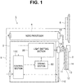
- a reference numeral 1 denotes an endoscope system that includes a scope 2, a light source apparatus 3, a video processor 4, a monitor 5, and a communication cable 6.
- the scope 2 is an endoscope that applies, to an object, light supplied from the light source apparatus 3, thereby enabling various kinds of observation and treatment to be performed.
- the scope 2 is connected to the light source apparatus 3 through a light guide connector 15, and is connected to the video processor 4 through a video connector 16.
- a proximal end of a light guide 11 that is inserted into the scope 2 is connected to the light guide connector 15, and a distal end of the light guide 11 is extended up to a distal end of an insertion portion of the scope 2.
- the light guide connector 15 is connected to the light source apparatus 3
- light from the light source apparatus 3 enters an incident end surface of the proximal end of the light guide 11, and light is outputted from an exit surface of the distal end of the light guide 11 at the distal end of the scope 2.
- a lens 12 is disposed in an optical path of the exit light at the distal end of the scope 2.
- the light that has been supplied from the light source apparatus 3 and has been transmitted inside the light guide 11 is applied to the object from the distal end of the insertion portion of the scope 2 through the lens 12.
- An optical image of the object that is irradiated with the light is taken through an unillustrated objective lens that is disposed at the distal end of the insertion portion of the scope 2, and the optical image is formed on an image pickup device 13 that converts the optical image into an electric signal.
- the image pickup device 13 is a solid-state image pickup device such as a CMOS and a CCD, and is configured as a color image pickup device in which a color filter array and the like are disposed, or a monochromatic image pickup device that receives frame-sequential illumination light.
- the image pickup device 13 converts the optical image of the object into an electric image pickup signal, and transmits, through a signal line 14, the image pickup signal to the video processor 4 to which the video connector 16 is connected.
- the video processor 4 processes the image pickup signal received from the image pickup device 13, to generate an image signal for display on a monitor 5. For example, the video processor 4 synchronizes the image pickup signals of respective colors provided from the image pickup device 13 to generate a color image signal. After performing image processing such as color balance adjustment, gamma conversion, and color conversion on the generated image signal, the video processor 4 converts the processed image signal into a signal of a format for display on the monitor 5, and outputs the converted signal to the monitor 5. As a result, the image of the object is displayed on the monitor 5.
- the video processor 4 extracts, for example, a luminance signal from the received image pickup signal, and generates brightness information based on the extracted luminance signal.
- the brightness information thus generated by the video processor 4 is transmitted to the light source apparatus 3 through the communication cable 6 that connects the video processor 4 to the light source apparatus 3.
- the light source apparatus 3 includes, as a main part, a light emitting section 20, a driving section 50, a control section 100, and an operation panel 110.
- the light source apparatus 3 can adjust intensity of the light to be supplied to the scope 2, and can supply light that is stable to environmental changes and individual variation.
- the light emitting section 20 includes, as a light source portion, a single or a plurality of light sources each generating light to be applied to the object, and supplies the generated light to the scope 2 through the light guide connector 15.
- a light source generating light for example, a light emitting device such as a xenon lamp and an LED is used.
- the light emitting section 20 includes an optical sensor 25 (see Fig. 2 ) that detects intensity of the light emitted by the light source.
- the driving section 50 includes a driving circuit that drives the light source of the light emitting section 20, a power supply circuit that supplies stabilized power of a predetermined voltage, and the like.
- the driving section 50 drives the light emitting device serving as the light source with a predetermined current, voltage, or frequency, thereby causing the light emitting device to generate a predetermined quantity of light. Operation of the driving section 50 is controlled by a control signal provided from the control section 100.
- the control section 100 controls the current, the voltage, or the frequency that is supplied to the light source of the light emitting section 20 through the driving section 50, thereby adjusting the intensity of the generated light. For example, the control section 100 varies the current to be supplied to the light source through PWM control, thereby adjusting light emission intensity of the light source.
- the light intensity adjustment is performed, based on input from the optical sensor 25, based on the brightness information of the object that is acquired in communication with the video processor 4 through the communication cable 6, or based on brightness setting of the illumination light by a user through the operation panel 110.
- the operation panel 110 allows the user to perform operation for the light source apparatus 3, and allows for operation such as power on/off of the light source apparatus 3, setting of an observation mode, and the brightness setting of the emission light.
- the set observation mode is transmitted to the video processor 4 through the control section 100 and the communication cable 6, and image processing corresponding to the observation mode is performed by the video processor 4.
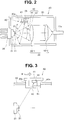
- Fig. 2 illustrates a configuration of the light emitting section 20.
- the light source portion that generates light to be applied to the object is configured of an LED 21.
- a lens system 22 for light guiding and light condensing is disposed in an optical path of the light emitted from the LED 21.
- the lens system 22 is an optical portion that receives a portion of the light emitted by the LED 21 and guides the received light, thereby forming an optical path to apply the light to the object.
- Fig. 2 illustrates an example in which light that has been received by a front lens 22-1 and has been converted into parallel light is condensed by a rear lens 22-2, and the condensed light enters a proximal end of a light guide 11a connected to the light guide connector 15.
- the LED 21 and the lens system 22 are housed in an optical case 30 serving as a dustproof first housing.
- An LED substrate 31 on which the LED 21 is mounted is disposed inside the optical case 30, and a heatsink 35 is in thermal contact with the LED substrate 31.
- the heatsink 35 is a heat dissipation member to dissipate, to the outside of the optical case 30, heat that is generated in light emission of the LED 21.
- the optical sensor 25 serving as a detection portion that detects intensity of the light, is disposed at a position that allows the optical sensor 25 to receive light other than the light entering the lens system 22 out of the light emitted by the LED 21, inside the optical case 30, in order to detect the intensity of the light without inhibiting the quantity of light emitted from the light source.
- the optical sensor 25 is housed in a dedicated photometric case 40 serving as a second housing.
- a light guide portion 42 that takes in the light emitted from the LED 21 is provided in the photometric case 40.
- the optical sensor 25 is attached on a sensor substrate 41 that forms a bottom surface surrounded by a side wall part 40a of the photometric case 40.
- the light guide portion 42 that takes in the light emitted from the LED 21 is provided on opening side of the side wall part 40a. The light guide portion 42 causes direct light from the LED 21 to enter the optical sensor 25, and inhibits scattered light and disturbance light from entering the optical sensor 25.
- the light guide portion 42 includes a transmission part 43 and a shielding part 44.
- the transmission part 43 is disposed in an optical path of the light that directly travels from the LED 21 to the optical sensor 25, out of the light emitted by the LED 21 at an angle between a maximum incident angle ⁇ i of the light to the lens system 22 and a maximum distribution angle ⁇ L of the light of the LED 21, and allows transmission of the light.
- the shielding part 44 prevents indirect light that is reflected or scattered inside the optical case 30, out of the light emitted by the LED 21, from entering the optical sensor 25.
- the side wall part 40a of the photometric case 40 forms a portion of the shielding part 44, and three-dimensionally surrounds the optical sensor 25.
- the shielding part 44 is made of a material that does not allow transmission of light, such as a metal material, and the transmission part 43 is formed as an opening hole surrounded by the shielding part 44.
- the opening part of the photometric case 40 is covered with a transparent member such as glass or a resin material, and the transparent member may be coated with a material that absorbs or reflects light, or the like. Then, the uncoated part may serve as the transmission part 43, and the coated part may serve as the shielding part 44.
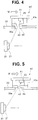
- the optical sensor 25 may be disposed as illustrated in Fig. 3 to Fig. 5 , with respect to the optical case 30.
- Fig. 3 to Fig. 5 each exemplify layout to suppress temperature increase of a peripheral portion of the optical sensor 25 caused by heat from the LED 21.
- the sensor substrate 41 on which the optical sensor 25 is mounted is used as a heat transfer portion that can transfer the heat of the optical sensor 25, and is disposed outside the optical case 30. More specifically, an opening part 30a is provided in the optical path of the direct light to the optical sensor 25 of the optical case 30, and the heat transfer portion of the optical sensor 25 is disposed outside the optical case 30 by fitting the side wall part 40a of the photometric case 40 to the opening part 30a to fix the photometric case 40 to the optical case 30.
- Such a layout makes it possible to secure a light entering path of the direct light from the LED 21 to the optical sensor 25 while preventing air and dust outside the optical case 30 from flowing into the optical case 30 and the photometric case 40 through the opening part 30a. Further, it is possible to effectively dissipate heat in the periphery of the optical sensor 25 from the sensor substrate 41, by cooling air W outside the optical case 30. As a result, it is possible to prevent deterioration of detection accuracy caused by temperature increase of the optical sensor 25, and to accurately adjust the intensity of the light emitted by the LED 21.
- Fig. 4 illustrates a layout example 2 in which a main body portion of a photometric case 40' is disposed outside the optical case 30.
- the photometric case 40' is changed in shape of the shielding part 44 of the photometric case 40.
- the photometric case 40' includes a shielding part 44' that projects forward, in contrast to the shielding part 44 of the photometric case 40.
- a projecting part of the shielding part 44' is fitted and fixed to the opening part 30a provided in the optical case 30 to dispose the main body portion of the photometric case 40' outside the optical case 30.
- Fig. 5 illustrates a layout example 3 in which the entire photometric case 40 is disposed outside the optical case 30.
- the light shielding part 44 of the photometric case 40 is brought into contact with and fixed to the optical case 30 so as to surround a peripheral edge of the opening part 30a provided in the optical case 30.
- Fig. 3 similarly to Fig. 3 , it is possible to prevent outside air and dust from entering the optical case 30 and the photometric case 40, and to secure the light entering path of the direct light from the LED 21 to the optical sensor 25, which allows for effective dissipation of the heat in the periphery of the optical sensor 25 by the cooling air W.
- the side wall part 40a and the shielding part 44 (44') may be configured as a heat insulation part made of a heat insulation member such as a resin material. This makes it possible to block heat transfer from the optical case 30 and the periphery of the optical case 30 to the optical sensor 25, and to accordingly prevent deterioration of detection accuracy caused by temperature increase of the optical sensor 25.
- the optical sensor 25 is disposed, as a positional condition, at a position between the maximum incident angle of the light to the lens system 22 and the maximum distribution angle of the light of the light source so as not to inhibit the emission quantity of the light from the light source.
- the lens system 22 guides and condenses the light from the light source.
- the optical sensor 25 may be provided at any position as long as satisfying the above-described positional condition.
- transmission parts 25A, 25B, and 25C that are provided to detect the light emission intensity of the respective light sources are disposed in respective regions illustrated by hatching in the drawing.
- the transmission parts 25A, 25B, and 25C are disposed in the respective regions between the maximum incident angles ⁇ iA, ⁇ iB, and ⁇ iC of light of the detection-objective light sources to respective lens systems 22A, 22B, and 22C and the maximum distribution angles ⁇ LA, ⁇ LB, and ⁇ LC of light of the respective detection-objective light sources, outside the maximum distribution angle of the adjacent detection-nonobjective light source. Deterioration of the detection accuracy of the transmission parts 25A, 25B, and 25C caused by the influence of the light from the adjacent light source is accordingly prevented.
- the transmission parts 25A, 25B, and 25C for the respective light sources are disposed such that the transmission part corresponding to the light source having low light emission intensity is adjacent to the transmission part corresponding to the light source having the high light emission intensity, even in the hatching region of Fig. 6 , the sensor for the light source having the low light emission intensity is influenced by the disturbance light of the light source having the high light emission intensity, and the detection accuracy of the sensor is accordingly deteriorated.
- the sensor is largely influenced by the detection-nonobjective light source in a case where the light source having the low light emission intensity and the light source having the high light emission intensity are adjacent to each other. Therefore, the sensor that detects the light source having the relatively low light emission intensity is provided at a position that is within the hatched region of Fig. 6 and is apart from the light source having the high light emission intensity, which prevents deterioration of the detection accuracy.
- the transmission part 25A that is provided to detect the light emission intensity of the LED 21A is disposed at a position apart from the LED 21B
- the transmission part 25C that is provided to detect the light emission intensity of the LED 21C is disposed at a position apart from the LED 21B, with respect to the transmission part 25B that is provided to detect the light emission intensity of the LED 21B. This allows each of the transmission part 25A that is provided to detect the light emission intensity of the LED 21A and the transmission part 25C that is provided to detect the light emission intensity of the LED 21C, to avoid influence of the LED 21B.
- the detection accuracy may be improved by providing light shielding plates 26A, 26B, and 26C among the adjacent LEDs 21A, 21B, and 21C.
- the light shielding plates 26A, 26B, and 26C may be integrally provided in the lens holding frames that respectively hold the lens systems 22A, 22B, and 22C, or may be added as separate components.
- the light shielding plates 26A, 26B, and 26C (hereinafter, collectively referred to as the light shielding plates 26) are provided as the separate components, a protrusion 27a or the like is provided on the lens holding frame 27 and the protrusion 27a is overlapped with each of the light shielding plates 26, which makes it possible to effectively prevent light leakage from a gap between the lens holding frame 27 and each of the light shielding plates 26.
- the light quantity of the LED 21 used as the light source of the light source apparatus 3 is typically adjusted through PWM control with a large current. To perform accurate control without disturbance in a PWM waveform, it is necessary to connect the driving circuit to the LED 21 with low resistance, and the driving circuit board is disposed near the LED 21. In addition, the optical sensor 25 that detects the light emission state of the LED 21 is disposed near the LED 21 for light detection.
- the pattern of the driving circuit board and the driving device become high temperature, and heat flows into the optical sensor 25 located in the vicinity, which may deteriorate the light detection accuracy. Accordingly, in the second embodiment, deterioration of the light detection accuracy is prevented by reducing heat inflow from the driving circuit board driving the LED 21 to the photometric case 40 housing the optical sensor 25 to maintain the optical sensor 25 at a given temperature or lower.
- the photometric case 40 is disposed outside the optical case 30 similarly to Fig. 5 , and the driving circuit board 51 that supplies a current to the LED 21 is disposed above the photometric case 40.
- the driving circuit board 51 is fixed to the outside of the optical case 30 through a substrate support 52, and is disposed with a predetermined interval from the sensor substrate 41 on which the optical sensor 25 is mounted.
- the driving circuit board 51 is connected, through a terminal portion 59 with low contact resistance, to the LED substrate 31 on which the LED 21 is mounted, and the LED 21 is driven by the driving device 55 on the driving circuit board 51.
- the heat generated when the driving device 55 drives the LED 21 is transferred and radiated from the substrate support 52 to the optical case 30 and is dissipated, through a path illustrated by a thick arrow in Fig. 10 . This prevents the heat from flowing into the photometric case 40. This makes it possible to suppress temperature increase of the optical sensor 25 and to prevent deterioration of the detection accuracy of the optical sensor 25.
- the sensor substrate 41 of the optical sensor 25 and the driving circuit board 51 may be configured as one circuit board 51A as illustrated in Fig. 11 in order to reduce an attachment space, improve assembling workability, and the like.
- Fig 11 illustrates an example in which the circuit board 51A is connected to the LED substrate 31 through an electric cable 33; however, the circuit board 51A may be connected to the LED substrate 31 through the terminal portion 59.
- a heat conduction prevention portion 56 that prevents heat conduction from the driving device 55 side to the optical sensor 25 side, is provided between the driving device 55 and the optical sensor 25 of the circuit board 51A.
- the heat conduction prevention portion 56 is formed of an elongated heat insulation member, an air layer of a slit, or the like provided between the driving device 55 and the optical sensor 25 of the circuit board 51A.
- the heat conduction prevention portion 56 blocks the heat conduction path from the driving device 55 to the optical sensor 25, thereby preventing deterioration of the detection accuracy of the optical sensor 25.
- a heat transfer component 57 serving as a heat path may be disposed in every heat conduction path from the driving device 55 to the optical sensor 25, to bring the heat transfer component 57 into thermal contact with a peripheral component 58. This makes it possible to dissipate heat from the driving device 55 to the peripheral component without forming the heat transfer path to the optical sensor 25 side, as illustrated by arrows in Fig. 13 , and to accordingly prevent deterioration of the detection accuracy of the optical sensor 25.
- the second embodiment it is possible to thermally shield the driving device 55 that is the driving heat generation device disposed near the LED 21 and the optical sensor 25 for light detection from each other, and to maintain the temperature of the optical sensor 25 to the given temperature or lower to secure light detection accuracy. As a result, it is possible to accurately adjust the intensity of the light emitted by the LED 21 to maintain a proper light emission state.
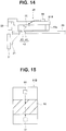
- the sensor substrate 41 on which the optical sensor 25 is mounted and the driving circuit board 51 also serve as one circuit board 51B, and the circuit board 51B forms a bottom surface part of a photometric case 45 housing the optical sensor 25, as illustrated in Fig. 14 .
- the circuit board 51B of the photometric case 45 is held by a side wall part 45a surrounding the optical sensor 25, and the light guide portion 42 to take in the light from the LED 21 is provided on opening side of the side wall part 45a.
- the light guide portion 42 includes the transmission part 43 and the shielding part 44, similarly to the photometric case 40.
- the transmission part 43 allows transmission of the direct light that directly enters the optical sensor 25 from the LED 21, and the shielding part 44 blocks indirect light that is reflected or scattered inside the optical case 30, from entering the optical sensor 25.
- the LED substrate 31 and the circuit board 51B are detachably connected to each other through the terminal portion 59 with low contact resistance.
- a surface ground layer 60 for common potential connection is formed on a board surface of the circuit board 51B on the driving device 55 side so as to traverse the heat conduction path between the driving device 55 and the optical sensor 25.
- the surface ground layer 60 functions as a heat dissipation layer that dissipates heat transferred from the driving device 55 to the surrounding atmosphere.
- the surface ground layer 60 is disposed over a board width between the driving device 55 and the optical sensor 25.
- the surface ground layer 60 may be formed as a surface ground layer 60A that is so disposed as to surround the driving device 55 in two directions inside the circuit board 51B.
- the surface ground layer 60 may be formed as a surface ground layer 60B that is so disposed as to surround the driving device 55 from four directions.
- the heat generated by the driving device 55 is transferred to the surface ground layer 60 (60A, or 60B) as illustrated by a solid arrow in Fig. 15 to Fig. 17 , and is dissipated to the surrounding atmosphere. Accordingly, movement of the heat to the optical sensor 25 side as illustrated by a dashed arrow in each of Fig. 15 to Fig. 17 is suppressed, which makes it possible to maintain the optical sensor 25 at the given temperature or lower to secure the light detection accuracy.
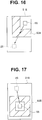
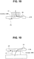
- a heat dissipation component 61 made of a heat conduction member or a heat diffusion member may be brought into thermal contact with the surface ground layer 60 (60A, or 60B), as illustrated in Fig. 18 and Fig. 19 .
- Fig. 18 illustrates an example in which the heat dissipation component 61 is brought into thermal contact with the surface ground layer 60 on the driving device 55 side of the circuit board 51B
- Fig. 19 illustrates an example in which the surface ground layer 60 is provided on the optical sensor 25 side of the circuit board 51B and the heat dissipation component 61 is brought into thermal contact with the surface ground layer 60.
- the heat dissipation component 61 is brought into thermal contact with the surface ground layer 60 (60A, or 60B), which allows for expansion of a heat dissipation area.
- the heat is dissipated from the heat dissipation component 61 to the surrounding components or the atmosphere, and the movement of the heat to the optical sensor 25 side is suppressed as well, which makes it possible to secure the light detection accuracy of the optical sensor 25.
- the third embodiment it is possible to thermally shield the driving device 55 and the optical sensor 25 that are disposed near the LED 21, to maintain the temperature of the optical sensor 25 to the predetermined temperature or lower to secure detection accuracy, and to maintain the proper light emission state of the LED 21, similarly to the second embodiment.
- connection between the LED substrate 31 on which the LED 21 is mounted and the driving circuit board 51 is described.
- the LED substrate 31 and the driving circuit board 51 are connected to each other through a substrate-mounted terminal in order to reduce electric resistance and to secure quality of a current waveform of the LED 21.
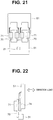
- a flat tab terminal (a male terminal) 70 is mounted as the substrate-mounted terminal on the LED substrate 31, and a female terminal 71 that is fitted to the flat tab terminal 70 of the LED substrate 31 is mounted on the driving circuit board 51. Further, the male terminal 70 and the female terminal 71 are fitted to each other, for example, in a direction as illustrated by an arrow in Fig. 20 , and the LED substrate 31 and the driving circuit board 51 are accordingly electrically connected to each other.
- the LED substrate 31 and the driving circuit board 51 that are electrically connected to each other through fitting of the terminals 70 and 71 are fixed to and supported by a predetermined portion outside the optical case 30 inside the light source apparatus 3.
- the LED substrate 31 is fixed to a first base 72 and is brought into thermal contact with a heatsink 35, and the driving circuit board 51 is fixed to a second base 73.
- contact resistance of the terminals 70 and 71 may be increased.
- a vibration load is applied in a direction substantially orthogonal to the fitting direction of the terminals 70 and 71
- damage is caused by small slip on a contact surface between the male terminal 70 of the LED substrate 31 and the female terminal 71 of the driving circuit board 51, and an oxide 74 is generated by so-called fretting corrosion.
- the oxide 74 may increase the contact resistance of the terminals 70 and 71 and may cause failure in the light emission of the LED 21 in some cases.
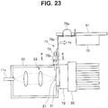
- the female terminal 75 includes a mounting part 75a, a fitting part 75b, and a coupling part 75c.
- the mounting part 75a is fixed to the driving circuit board 51.
- the fitting part 75b is fitted to the male terminal 70 of the LED substrate 31.
- the coupling part 75c couples the mounting part 75a with the fitting part 75b.
- the mounting part 75a includes a plurality of plate-like protrusion pieces 75al that are fitted to the driving circuit board 51.
- the mounting part 75a is fixed to the driving circuit board 51 through soldering or the like after the protrusion pieces 75al are fitted into the driving circuit board 51.
- the coupling part 75c that couples the mounting part 75a with the fitting part 75b is formed in a flat plate shape, is extended from the fitting part 75b in the same direction as the fitting direction, and is coupled to the mounting part 75a so as to be substantially orthogonal to the driving circuit board 51.
- the fitting part 75b that is coupled to the mounting part 75a through such a plate-like coupling part 75c has a shape to sandwich a flat surface part of the male terminal 70 from both sides as illustrated in Fig. 25 .
- the fitting part 75b is set in relationship that pressing force Fh that sandwiches and holds the flat surface part of the male terminal 70 becomes larger than force Fd applied to the coupling part 75c when receiving the vibration load (Fh>Fd).
- the coupling part 75c is deformed and displaced with smaller force prior to the fitting part 75b, and displacement and abrasion between the male terminal 70 and the female terminal 71 on the surface of the fitting part are reduced, which makes it possible to prevent increase of the contact resistance caused by corrosion of the contact surface even in a case where the first base 72 to which the LED substrate 31 is fixed and the second base 73 to which the driving circuit board 51 is fixed are relatively swung by the vibration load.
Landscapes
- Health & Medical Sciences (AREA)
- Life Sciences & Earth Sciences (AREA)
- Physics & Mathematics (AREA)
- Surgery (AREA)
- Optics & Photonics (AREA)
- Engineering & Computer Science (AREA)
- Biomedical Technology (AREA)
- Veterinary Medicine (AREA)
- Pathology (AREA)
- Radiology & Medical Imaging (AREA)
- Biophysics (AREA)
- Nuclear Medicine, Radiotherapy & Molecular Imaging (AREA)
- Public Health (AREA)
- Heart & Thoracic Surgery (AREA)
- Medical Informatics (AREA)
- Molecular Biology (AREA)
- Animal Behavior & Ethology (AREA)
- General Health & Medical Sciences (AREA)
- General Physics & Mathematics (AREA)
- Astronomy & Astrophysics (AREA)
- Microelectronics & Electronic Packaging (AREA)
- Endoscopes (AREA)
- Investigating Or Analysing Materials By Optical Means (AREA)
- Instruments For Viewing The Inside Of Hollow Bodies (AREA)
Abstract
Description
- The present invention relates to a light source apparatus that detects emission intensity of light emitted by a light source while applying the light to an object.
- Some of existing light source apparatuses that supply, to an endoscope and the like, light applied to an object adopt a system that measures a quantity of light emitted by a light source in order to adjust the quantity of the light of the light source, and the measured light quantity is fed back to a control section to control the light quantity to an appropriate amount.
- For example, Japanese Patent No.
5393935 - Further, Japanese Patent Application Laid-Open Publication No.
2015-19695 - In the existing light source apparatuses as disclosed in Japanese Patent No.
5393935 2015-19695 - The present invention is made in consideration of the above-described circumstances, and an object of the present invention is to provide a light source apparatus that makes it possible to accurately detect only light in a direct optical path from a light source, out of light emitted by a light source.
- A light source apparatus according to an aspect of the present invention includes: a light source portion configured to emit light applied to an object; an optical portion configured to receive a portion of the light emitted by the light source portion, and to form an optical path to apply the received light to the object; a detection portion that is disposed at a position allowing the detection portion to receive light other than the light received by the optical portion, out of the light emitted by the light source portion, and is configured to detect intensity of the received light; a transmission part that is disposed in an optical path of light that directly travels from the light source portion to the detection portion out of the light emitted by the light source portion, and is configured to allow transmission of the light; and a shielding part configured to block indirect light that is generated by reflection or scattering of the light emitted by the light source portion, from entering the detection portion.
-
-
Fig. 1 is a configuration diagram of an endoscope system according to a first embodiment of the present invention; -
Fig. 2 is an explanatory diagram illustrating a configuration of a light emitting section according to the first embodiment of the present invention; -
Fig. 3 is an explanatory diagram illustrating a layout example 1 of an optical sensor according to the first embodiment of the present invention; -
Fig. 4 is an explanatory diagram illustrating a layout example 2 of the optical sensor according to the first embodiment of the present invention; -
Fig. 5 is an explanatory diagram illustrating a layout example 3 of the optical sensor according to the first embodiment of the present invention; -
Fig. 6 is an explanatory diagram illustrating a layout example 1 of a transmission part for each light source according to the first embodiment of the present invention; -
Fig. 7 is an explanatory diagram illustrating a layout example 2 of the transmission part for each light source according to the first embodiment of the present invention; -
Fig. 8 is an explanatory diagram illustrating an example in which a light shielding plate is provided between the light sources according to the first embodiment of the present invention; -
Fig. 9 is an explanatory diagram illustrating the light shielding plate and a lens holding frame according to the first embodiment of the present invention; -
Fig. 10 is an explanatory diagram illustrating layout of a photometric case and a driving circuit board according to a second embodiment of the present invention; -
Fig. 11 is an explanatory diagram illustrating an example in which a sensor substrate and the driving circuit board are integrated according to the second embodiment of the present invention; -
Fig. 12 is a plan view of the circuit board according to the second embodiment of the present invention; -
Fig. 13 is an explanatory diagram illustrating a heat conduction path from a driving device according to the second embodiment of the present invention; -
Fig. 14 is an explanatory diagram of a photometric case according to a third embodiment of the present invention; -
Fig. 15 is an explanatory diagram illustrating an example of a surface ground layer of a circuit board according to the third embodiment of the present invention; -
Fig. 16 is an explanatory diagram illustrating another example of the surface ground layer of the circuit board according to the third embodiment of the present invention; -
Fig. 17 is an explanatory diagram illustrating still another example of the surface ground layer of the circuit board according to the third embodiment of the present invention; -
Fig. 18 is an explanatory diagram illustrating an example in which a heat dissipation component is brought into thermal contact with the surface ground layer on driving device side according to the third embodiment of the present invention; -
Fig. 19 is an explanatory diagram illustrating an example in which a heat dissipation component is brought into thermal contact with the surface ground layer on optical sensor side according to the third embodiment of the present invention; -
Fig. 20 is an explanatory diagram illustrating connection between an LED substrate and the driving circuit board according to the third embodiment of the present invention; -
Fig. 21 is a front view of the LED substrate and the driving circuit board according to the third embodiment of the present invention; -
Fig. 22 is an explanatory diagram illustrating an oxide that is generated on a terminal contact surface by vibration according to the third embodiment of the present invention; -
Fig. 23 is an explanatory diagram illustrating connection between the LED substrate and the driving circuit board that copes with vibration load according to the third embodiment of the present invention; -
Fig. 24 is an explanatory diagram illustrating a mounting part of a female terminal fixed to the driving circuit board according to the third embodiment of the present invention; and -
Fig. 25 is a cross-sectional diagram taken along line A-A inFig. 23 according to the third embodiment of the present invention. - Embodiments of the present invention are described below with reference to drawings.
- In
Fig. 1 , areference numeral 1 denotes an endoscope system that includes ascope 2, alight source apparatus 3, avideo processor 4, amonitor 5, and acommunication cable 6. Thescope 2 is an endoscope that applies, to an object, light supplied from thelight source apparatus 3, thereby enabling various kinds of observation and treatment to be performed. Thescope 2 is connected to thelight source apparatus 3 through alight guide connector 15, and is connected to thevideo processor 4 through avideo connector 16. - A proximal end of a
light guide 11 that is inserted into thescope 2 is connected to thelight guide connector 15, and a distal end of thelight guide 11 is extended up to a distal end of an insertion portion of thescope 2. When thelight guide connector 15 is connected to thelight source apparatus 3, light from thelight source apparatus 3 enters an incident end surface of the proximal end of thelight guide 11, and light is outputted from an exit surface of the distal end of thelight guide 11 at the distal end of thescope 2. - A
lens 12 is disposed in an optical path of the exit light at the distal end of thescope 2. The light that has been supplied from thelight source apparatus 3 and has been transmitted inside thelight guide 11 is applied to the object from the distal end of the insertion portion of thescope 2 through thelens 12. An optical image of the object that is irradiated with the light is taken through an unillustrated objective lens that is disposed at the distal end of the insertion portion of thescope 2, and the optical image is formed on animage pickup device 13 that converts the optical image into an electric signal. - The
image pickup device 13 is a solid-state image pickup device such as a CMOS and a CCD, and is configured as a color image pickup device in which a color filter array and the like are disposed, or a monochromatic image pickup device that receives frame-sequential illumination light. Theimage pickup device 13 converts the optical image of the object into an electric image pickup signal, and transmits, through asignal line 14, the image pickup signal to thevideo processor 4 to which thevideo connector 16 is connected. - The
video processor 4 processes the image pickup signal received from theimage pickup device 13, to generate an image signal for display on amonitor 5. For example, thevideo processor 4 synchronizes the image pickup signals of respective colors provided from theimage pickup device 13 to generate a color image signal. After performing image processing such as color balance adjustment, gamma conversion, and color conversion on the generated image signal, thevideo processor 4 converts the processed image signal into a signal of a format for display on themonitor 5, and outputs the converted signal to themonitor 5. As a result, the image of the object is displayed on themonitor 5. - Further, the
video processor 4 extracts, for example, a luminance signal from the received image pickup signal, and generates brightness information based on the extracted luminance signal. The brightness information thus generated by thevideo processor 4 is transmitted to thelight source apparatus 3 through thecommunication cable 6 that connects thevideo processor 4 to thelight source apparatus 3. - Next, an internal configuration of the
light source apparatus 3 is described. Thelight source apparatus 3 includes, as a main part, alight emitting section 20, adriving section 50, acontrol section 100, and anoperation panel 110. Thelight source apparatus 3 can adjust intensity of the light to be supplied to thescope 2, and can supply light that is stable to environmental changes and individual variation. - The
light emitting section 20 includes, as a light source portion, a single or a plurality of light sources each generating light to be applied to the object, and supplies the generated light to thescope 2 through thelight guide connector 15. As the light source generating light, for example, a light emitting device such as a xenon lamp and an LED is used. As described later, thelight emitting section 20 includes an optical sensor 25 (seeFig. 2 ) that detects intensity of the light emitted by the light source. - The
driving section 50 includes a driving circuit that drives the light source of thelight emitting section 20, a power supply circuit that supplies stabilized power of a predetermined voltage, and the like. Thedriving section 50 drives the light emitting device serving as the light source with a predetermined current, voltage, or frequency, thereby causing the light emitting device to generate a predetermined quantity of light. Operation of thedriving section 50 is controlled by a control signal provided from thecontrol section 100. - The
control section 100 controls the current, the voltage, or the frequency that is supplied to the light source of thelight emitting section 20 through the drivingsection 50, thereby adjusting the intensity of the generated light. For example, thecontrol section 100 varies the current to be supplied to the light source through PWM control, thereby adjusting light emission intensity of the light source. The light intensity adjustment is performed, based on input from theoptical sensor 25, based on the brightness information of the object that is acquired in communication with thevideo processor 4 through thecommunication cable 6, or based on brightness setting of the illumination light by a user through theoperation panel 110. - The
operation panel 110 allows the user to perform operation for thelight source apparatus 3, and allows for operation such as power on/off of thelight source apparatus 3, setting of an observation mode, and the brightness setting of the emission light. When the user operates theoperation panel 110 to set a desired observation mode, the set observation mode is transmitted to thevideo processor 4 through thecontrol section 100 and thecommunication cable 6, and image processing corresponding to the observation mode is performed by thevideo processor 4. -
Fig. 2 illustrates a configuration of thelight emitting section 20. In the present embodiment, the light source portion that generates light to be applied to the object is configured of anLED 21. Alens system 22 for light guiding and light condensing is disposed in an optical path of the light emitted from theLED 21. Thelens system 22 is an optical portion that receives a portion of the light emitted by theLED 21 and guides the received light, thereby forming an optical path to apply the light to the object.Fig. 2 illustrates an example in which light that has been received by a front lens 22-1 and has been converted into parallel light is condensed by a rear lens 22-2, and the condensed light enters a proximal end of alight guide 11a connected to thelight guide connector 15. - The
LED 21 and thelens system 22 are housed in anoptical case 30 serving as a dustproof first housing. AnLED substrate 31 on which theLED 21 is mounted is disposed inside theoptical case 30, and aheatsink 35 is in thermal contact with theLED substrate 31. Theheatsink 35 is a heat dissipation member to dissipate, to the outside of theoptical case 30, heat that is generated in light emission of theLED 21. - Further, the
optical sensor 25 serving as a detection portion that detects intensity of the light, is disposed at a position that allows theoptical sensor 25 to receive light other than the light entering thelens system 22 out of the light emitted by theLED 21, inside theoptical case 30, in order to detect the intensity of the light without inhibiting the quantity of light emitted from the light source. Theoptical sensor 25 is housed in a dedicatedphotometric case 40 serving as a second housing. Alight guide portion 42 that takes in the light emitted from theLED 21 is provided in thephotometric case 40. - More specifically, the
optical sensor 25 is attached on asensor substrate 41 that forms a bottom surface surrounded by aside wall part 40a of thephotometric case 40. Thelight guide portion 42 that takes in the light emitted from theLED 21 is provided on opening side of theside wall part 40a. Thelight guide portion 42 causes direct light from theLED 21 to enter theoptical sensor 25, and inhibits scattered light and disturbance light from entering theoptical sensor 25. - More specifically, the
light guide portion 42 includes atransmission part 43 and a shieldingpart 44. Thetransmission part 43 is disposed in an optical path of the light that directly travels from theLED 21 to theoptical sensor 25, out of the light emitted by theLED 21 at an angle between a maximum incident angle θi of the light to thelens system 22 and a maximum distribution angle θL of the light of theLED 21, and allows transmission of the light. The shieldingpart 44 prevents indirect light that is reflected or scattered inside theoptical case 30, out of the light emitted by theLED 21, from entering theoptical sensor 25. Theside wall part 40a of thephotometric case 40 forms a portion of the shieldingpart 44, and three-dimensionally surrounds theoptical sensor 25. As a result, it is possible to remove the indirect light that is varied by influence of environmental change such as ambient temperature, and individual variation for each apparatus, and to accurately detect only the direct light from theLED 21, thereby measuring the light quantity stably and accurately. - In the present embodiment, the shielding
part 44 is made of a material that does not allow transmission of light, such as a metal material, and thetransmission part 43 is formed as an opening hole surrounded by the shieldingpart 44. Note that the opening part of thephotometric case 40 is covered with a transparent member such as glass or a resin material, and the transparent member may be coated with a material that absorbs or reflects light, or the like. Then, the uncoated part may serve as thetransmission part 43, and the coated part may serve as the shieldingpart 44. - Here, the
optical sensor 25 may be disposed as illustrated inFig. 3 to Fig. 5 , with respect to theoptical case 30.Fig. 3 to Fig. 5 each exemplify layout to suppress temperature increase of a peripheral portion of theoptical sensor 25 caused by heat from theLED 21. - In a layout example 1 of the
optical sensor 25 illustrated inFig. 3 , thesensor substrate 41 on which theoptical sensor 25 is mounted is used as a heat transfer portion that can transfer the heat of theoptical sensor 25, and is disposed outside theoptical case 30. More specifically, anopening part 30a is provided in the optical path of the direct light to theoptical sensor 25 of theoptical case 30, and the heat transfer portion of theoptical sensor 25 is disposed outside theoptical case 30 by fitting theside wall part 40a of thephotometric case 40 to theopening part 30a to fix thephotometric case 40 to theoptical case 30. - Such a layout makes it possible to secure a light entering path of the direct light from the
LED 21 to theoptical sensor 25 while preventing air and dust outside theoptical case 30 from flowing into theoptical case 30 and thephotometric case 40 through theopening part 30a. Further, it is possible to effectively dissipate heat in the periphery of theoptical sensor 25 from thesensor substrate 41, by cooling air W outside theoptical case 30. As a result, it is possible to prevent deterioration of detection accuracy caused by temperature increase of theoptical sensor 25, and to accurately adjust the intensity of the light emitted by theLED 21. - Further,
Fig. 4 illustrates a layout example 2 in which a main body portion of a photometric case 40' is disposed outside theoptical case 30. The photometric case 40' is changed in shape of the shieldingpart 44 of thephotometric case 40. The photometric case 40' includes a shielding part 44' that projects forward, in contrast to the shieldingpart 44 of thephotometric case 40. A projecting part of the shielding part 44' is fitted and fixed to theopening part 30a provided in theoptical case 30 to dispose the main body portion of the photometric case 40' outside theoptical case 30. - As a result, similarly to
Fig. 3 , it is possible to prevent outside air and dust from entering theoptical case 30 and thephotometric case 40, and to secure the light entering path of the direct light from theLED 21 to theoptical sensor 25, which allows for effective dissipation of the heat in the periphery of theoptical sensor 25 by the cooling air W. -
Fig. 5 illustrates a layout example 3 in which the entirephotometric case 40 is disposed outside theoptical case 30. Thelight shielding part 44 of thephotometric case 40 is brought into contact with and fixed to theoptical case 30 so as to surround a peripheral edge of theopening part 30a provided in theoptical case 30. As a result, similarly toFig. 3 , it is possible to prevent outside air and dust from entering theoptical case 30 and thephotometric case 40, and to secure the light entering path of the direct light from theLED 21 to theoptical sensor 25, which allows for effective dissipation of the heat in the periphery of theoptical sensor 25 by the cooling air W. - In addition, in the photometric case 40 (40'), the
side wall part 40a and the shielding part 44 (44') may be configured as a heat insulation part made of a heat insulation member such as a resin material. This makes it possible to block heat transfer from theoptical case 30 and the periphery of theoptical case 30 to theoptical sensor 25, and to accordingly prevent deterioration of detection accuracy caused by temperature increase of theoptical sensor 25. - Next, in a case where a plurality of light sources are adjacently disposed in the
optical case 30, layout of theoptical sensors 25 provided correspondingly to the plurality of light sources is described. - As described above, the
optical sensor 25 is disposed, as a positional condition, at a position between the maximum incident angle of the light to thelens system 22 and the maximum distribution angle of the light of the light source so as not to inhibit the emission quantity of the light from the light source. Thelens system 22 guides and condenses the light from the light source. In a case of a single light source, theoptical sensor 25 may be provided at any position as long as satisfying the above-described positional condition. In contrast, in a case where the plurality of light sources are adjacently arranged, it is necessary to consider influence of light from the adjacent light source, in theoptical sensors 25 that are provided correspondingly to the respective light sources. - For example, as illustrated in
Fig. 6 , in a case where threeLEDs transmission parts - In other words, the
transmission parts respective lens systems transmission parts - Further, in a case where influence of feeble scattering light and the like that is present outside the maximum distribution angle of the detection-nonobjective light source is not ignorable, improvement of the detection accuracy is achieved by providing the
transmission parts - For example, in a case where the light emission intensity of the
respective LEDs transmission parts Fig. 6 , the sensor for the light source having the low light emission intensity is influenced by the disturbance light of the light source having the high light emission intensity, and the detection accuracy of the sensor is accordingly deteriorated. - The sensor is largely influenced by the detection-nonobjective light source in a case where the light source having the low light emission intensity and the light source having the high light emission intensity are adjacent to each other. Therefore, the sensor that detects the light source having the relatively low light emission intensity is provided at a position that is within the hatched region of
Fig. 6 and is apart from the light source having the high light emission intensity, which prevents deterioration of the detection accuracy. - For example, in a case where the
LED 21B has the highest light emission intensity among theLEDs Fig. 7 , thetransmission part 25A that is provided to detect the light emission intensity of theLED 21A is disposed at a position apart from theLED 21B, and thetransmission part 25C that is provided to detect the light emission intensity of theLED 21C is disposed at a position apart from theLED 21B, with respect to thetransmission part 25B that is provided to detect the light emission intensity of theLED 21B. This allows each of thetransmission part 25A that is provided to detect the light emission intensity of theLED 21A and thetransmission part 25C that is provided to detect the light emission intensity of theLED 21C, to avoid influence of theLED 21B. - In this case, as illustrated in
Fig. 8 , the detection accuracy may be improved by providinglight shielding plates adjacent LEDs light shielding plates lens systems - In a case where the
light shielding plates protrusion 27a or the like is provided on thelens holding frame 27 and theprotrusion 27a is overlapped with each of the light shielding plates 26, which makes it possible to effectively prevent light leakage from a gap between thelens holding frame 27 and each of the light shielding plates 26. - Next, a second embodiment of the present invention is described. The light quantity of the
LED 21 used as the light source of thelight source apparatus 3 is typically adjusted through PWM control with a large current. To perform accurate control without disturbance in a PWM waveform, it is necessary to connect the driving circuit to theLED 21 with low resistance, and the driving circuit board is disposed near theLED 21. In addition, theoptical sensor 25 that detects the light emission state of theLED 21 is disposed near theLED 21 for light detection. - When a large current is applied to the
LED 21 in such layout, the pattern of the driving circuit board and the driving device become high temperature, and heat flows into theoptical sensor 25 located in the vicinity, which may deteriorate the light detection accuracy. Accordingly, in the second embodiment, deterioration of the light detection accuracy is prevented by reducing heat inflow from the driving circuit board driving theLED 21 to thephotometric case 40 housing theoptical sensor 25 to maintain theoptical sensor 25 at a given temperature or lower. - As illustrated in
Fig. 10 , thephotometric case 40 is disposed outside theoptical case 30 similarly toFig. 5 , and the drivingcircuit board 51 that supplies a current to theLED 21 is disposed above thephotometric case 40. The drivingcircuit board 51 is fixed to the outside of theoptical case 30 through asubstrate support 52, and is disposed with a predetermined interval from thesensor substrate 41 on which theoptical sensor 25 is mounted. - The driving
circuit board 51 is connected, through aterminal portion 59 with low contact resistance, to theLED substrate 31 on which theLED 21 is mounted, and theLED 21 is driven by the drivingdevice 55 on the drivingcircuit board 51. The heat generated when the drivingdevice 55 drives theLED 21 is transferred and radiated from thesubstrate support 52 to theoptical case 30 and is dissipated, through a path illustrated by a thick arrow inFig. 10 . This prevents the heat from flowing into thephotometric case 40. This makes it possible to suppress temperature increase of theoptical sensor 25 and to prevent deterioration of the detection accuracy of theoptical sensor 25. - Note that the
sensor substrate 41 of theoptical sensor 25 and the drivingcircuit board 51 may be configured as onecircuit board 51A as illustrated inFig. 11 in order to reduce an attachment space, improve assembling workability, and the like.Fig 11 illustrates an example in which thecircuit board 51A is connected to theLED substrate 31 through anelectric cable 33; however, thecircuit board 51A may be connected to theLED substrate 31 through theterminal portion 59. - In this case, as illustrated in
Fig. 12 , a heatconduction prevention portion 56 that prevents heat conduction from the drivingdevice 55 side to theoptical sensor 25 side, is provided between the drivingdevice 55 and theoptical sensor 25 of thecircuit board 51A. The heatconduction prevention portion 56 is formed of an elongated heat insulation member, an air layer of a slit, or the like provided between the drivingdevice 55 and theoptical sensor 25 of thecircuit board 51A. The heatconduction prevention portion 56 blocks the heat conduction path from the drivingdevice 55 to theoptical sensor 25, thereby preventing deterioration of the detection accuracy of theoptical sensor 25. - Further, as illustrated in
Fig. 13 , aheat transfer component 57 serving as a heat path may be disposed in every heat conduction path from the drivingdevice 55 to theoptical sensor 25, to bring theheat transfer component 57 into thermal contact with aperipheral component 58. This makes it possible to dissipate heat from the drivingdevice 55 to the peripheral component without forming the heat transfer path to theoptical sensor 25 side, as illustrated by arrows inFig. 13 , and to accordingly prevent deterioration of the detection accuracy of theoptical sensor 25. - In the second embodiment, it is possible to thermally shield the driving
device 55 that is the driving heat generation device disposed near theLED 21 and theoptical sensor 25 for light detection from each other, and to maintain the temperature of theoptical sensor 25 to the given temperature or lower to secure light detection accuracy. As a result, it is possible to accurately adjust the intensity of the light emitted by theLED 21 to maintain a proper light emission state. - Next, a third embodiment of the present invention is described. In contrast to the second embodiment, in the third embodiment, the
sensor substrate 41 on which theoptical sensor 25 is mounted and the drivingcircuit board 51 also serve as onecircuit board 51B, and thecircuit board 51B forms a bottom surface part of aphotometric case 45 housing theoptical sensor 25, as illustrated inFig. 14 . - More specifically, the
circuit board 51B of thephotometric case 45 according to the third embodiment is held by aside wall part 45a surrounding theoptical sensor 25, and thelight guide portion 42 to take in the light from theLED 21 is provided on opening side of theside wall part 45a. Thelight guide portion 42 includes thetransmission part 43 and the shieldingpart 44, similarly to thephotometric case 40. Thetransmission part 43 allows transmission of the direct light that directly enters theoptical sensor 25 from theLED 21, and the shieldingpart 44 blocks indirect light that is reflected or scattered inside theoptical case 30, from entering theoptical sensor 25. TheLED substrate 31 and thecircuit board 51B are detachably connected to each other through theterminal portion 59 with low contact resistance. - As illustrated in
Fig. 15 , asurface ground layer 60 for common potential connection is formed on a board surface of thecircuit board 51B on the drivingdevice 55 side so as to traverse the heat conduction path between the drivingdevice 55 and theoptical sensor 25. Thesurface ground layer 60 functions as a heat dissipation layer that dissipates heat transferred from the drivingdevice 55 to the surrounding atmosphere. InFig. 15 , thesurface ground layer 60 is disposed over a board width between the drivingdevice 55 and theoptical sensor 25. - Further, as illustrated in
Fig. 16 , thesurface ground layer 60 may be formed as asurface ground layer 60A that is so disposed as to surround the drivingdevice 55 in two directions inside thecircuit board 51B. Moreover, as illustrated inFig. 17 , thesurface ground layer 60 may be formed as asurface ground layer 60B that is so disposed as to surround the drivingdevice 55 from four directions. - When the surface ground layer 60 (60A, or 60B) is provided, the heat generated by the driving
device 55 is transferred to the surface ground layer 60 (60A, or 60B) as illustrated by a solid arrow inFig. 15 to Fig. 17 , and is dissipated to the surrounding atmosphere. Accordingly, movement of the heat to theoptical sensor 25 side as illustrated by a dashed arrow in each ofFig. 15 to Fig. 17 is suppressed, which makes it possible to maintain theoptical sensor 25 at the given temperature or lower to secure the light detection accuracy. - In this case, to further promote heat dissipation from the surface ground layer 60 (60A, or 60B), a
heat dissipation component 61 made of a heat conduction member or a heat diffusion member may be brought into thermal contact with the surface ground layer 60 (60A, or 60B), as illustrated inFig. 18 and Fig. 19 . - Note that
Fig. 18 illustrates an example in which theheat dissipation component 61 is brought into thermal contact with thesurface ground layer 60 on the drivingdevice 55 side of thecircuit board 51B, andFig. 19 illustrates an example in which thesurface ground layer 60 is provided on theoptical sensor 25 side of thecircuit board 51B and theheat dissipation component 61 is brought into thermal contact with thesurface ground layer 60. - As described above, the
heat dissipation component 61 is brought into thermal contact with the surface ground layer 60 (60A, or 60B), which allows for expansion of a heat dissipation area. The heat is dissipated from theheat dissipation component 61 to the surrounding components or the atmosphere, and the movement of the heat to theoptical sensor 25 side is suppressed as well, which makes it possible to secure the light detection accuracy of theoptical sensor 25. - Also in the third embodiment, it is possible to thermally shield the driving
device 55 and theoptical sensor 25 that are disposed near theLED 21, to maintain the temperature of theoptical sensor 25 to the predetermined temperature or lower to secure detection accuracy, and to maintain the proper light emission state of theLED 21, similarly to the second embodiment. - Here, connection between the
LED substrate 31 on which theLED 21 is mounted and the drivingcircuit board 51 is described. TheLED substrate 31 and the drivingcircuit board 51 are connected to each other through a substrate-mounted terminal in order to reduce electric resistance and to secure quality of a current waveform of theLED 21. - For example, as illustrated in
Fig. 20 andFig. 21 , a flat tab terminal (a male terminal) 70 is mounted as the substrate-mounted terminal on theLED substrate 31, and afemale terminal 71 that is fitted to theflat tab terminal 70 of theLED substrate 31 is mounted on the drivingcircuit board 51. Further, themale terminal 70 and thefemale terminal 71 are fitted to each other, for example, in a direction as illustrated by an arrow inFig. 20 , and theLED substrate 31 and the drivingcircuit board 51 are accordingly electrically connected to each other. - The
LED substrate 31 and the drivingcircuit board 51 that are electrically connected to each other through fitting of theterminals optical case 30 inside thelight source apparatus 3. TheLED substrate 31 is fixed to afirst base 72 and is brought into thermal contact with aheatsink 35, and the drivingcircuit board 51 is fixed to asecond base 73. - When a vibration load is applied to the entire
light source apparatus 3 during transportation or the like, however, contact resistance of theterminals Fig. 22 , when a vibration load is applied in a direction substantially orthogonal to the fitting direction of theterminals male terminal 70 of theLED substrate 31 and thefemale terminal 71 of the drivingcircuit board 51, and anoxide 74 is generated by so-called fretting corrosion. Theoxide 74 may increase the contact resistance of theterminals LED 21 in some cases. - In contrast, connecting the
female terminal 71 of the drivingcircuit board 51 as afemale terminal 75 having a shape illustrated inFig. 23 to themale terminal 70 of theLED substrate 31 makes it possible to prevent increase of the contact resistance at the contact caused by the vibration load. Thefemale terminal 75 includes a mountingpart 75a, afitting part 75b, and acoupling part 75c. The mountingpart 75a is fixed to the drivingcircuit board 51. Thefitting part 75b is fitted to themale terminal 70 of theLED substrate 31. Thecoupling part 75c couples the mountingpart 75a with thefitting part 75b. - As illustrated in
Fig. 24 , the mountingpart 75a includes a plurality of plate-like protrusion pieces 75al that are fitted to the drivingcircuit board 51. The mountingpart 75a is fixed to the drivingcircuit board 51 through soldering or the like after the protrusion pieces 75al are fitted into the drivingcircuit board 51. Thecoupling part 75c that couples the mountingpart 75a with thefitting part 75b is formed in a flat plate shape, is extended from thefitting part 75b in the same direction as the fitting direction, and is coupled to the mountingpart 75a so as to be substantially orthogonal to the drivingcircuit board 51. - The
fitting part 75b that is coupled to the mountingpart 75a through such a plate-like coupling part 75c has a shape to sandwich a flat surface part of the male terminal 70 from both sides as illustrated inFig. 25 . Thefitting part 75b is set in relationship that pressing force Fh that sandwiches and holds the flat surface part of themale terminal 70 becomes larger than force Fd applied to thecoupling part 75c when receiving the vibration load (Fh>Fd). - When the
fitting part 75b is set in such relationship, thecoupling part 75c is deformed and displaced with smaller force prior to thefitting part 75b, and displacement and abrasion between themale terminal 70 and thefemale terminal 71 on the surface of the fitting part are reduced, which makes it possible to prevent increase of the contact resistance caused by corrosion of the contact surface even in a case where thefirst base 72 to which theLED substrate 31 is fixed and thesecond base 73 to which thedriving circuit board 51 is fixed are relatively swung by the vibration load. - As a result, it is possible to prevent lighting failure of the
LED 21 even if the vibration load is applied to the electrical connection part between theLED substrate 31 and the drivingcircuit board 51. Further, setting the fitting direction of thefemale terminal 71 connected to themale terminal 70 of theLED substrate 31 to the direction perpendicular to the drivingcircuit board 51 allows for arrangement of the drivingcircuit board 51 in the direction along theoptical case 30, which makes it possible to downsize the entire apparatus. - The present application is based upon and claims the benefit of priority of the Japanese Patent Application No.
2015-089708
Claims (10)
- A light source apparatus, comprising:a light source portion configured to emit light applied to an object;an optical portion configured to receive a portion of the light emitted by the light source portion, and to form an optical path to apply the received light to the object;a detection portion that is disposed at a position allowing the detection portion to receive light other than the light received by the optical portion, out of the light emitted by the light source portion, and is configured to detect intensity of the received light;a transmission part that is disposed in an optical path of light that directly travels from the light source portion to the detection portion out of the light emitted by the light source portion, and is configured to allow transmission of the light; anda shielding part configured to block indirect light from entering the detection portion, the indirect light being generated by reflection or scattering of the light emitted by the light source portion.
- The light source apparatus according to claim 1, wherein
the light source portion includes a plurality of light sources that are disposed adjacently to one another, and
the transmission part that is provided correspondingly to each of the plurality of light sources is disposed in a region between a maximum incident angle of light of a detection-objective light source to the optical portion and a maximum distribution angle of the light of the detection-objective light source, outside a maximum distribution angle of light of an adjacent detection-nonobjective light source. - The light source apparatus according to claim 2, wherein
the light source portion includes a first light source and a second light source that is higher in light emission intensity than the first light source, and
the transmission part provided correspondingly to the first light source is provided at a position apart from the second light source with respect to the first light source. - The light source apparatus according to claim 1, wherein the shielding part is configured to three-dimensionally surround the detection portion.
- The light source apparatus according to claim 1, further comprising:a housing in which the light source portion and the optical portion are disposed; anda heat transfer portion configured to transfer heat of the detection portion, whereinthe heat transfer section is disposed outside the housing.
- The light source apparatus according to claim 4, wherein
the detection portion is provided outside the housing,
the housing includes an opening in the optical path of the direct light, and
the shielding part is provided to surround the opening to prevent air outside the housing from flowing into inside of the housing through the opening. - The light source apparatus according to claim 4, wherein
the detection portion is provided outside the housing,
the housing includes an opening in the optical path of the direct light, and
the shielding part is provided to be fitted to the opening, to prevent air outside the housing from flowing into inside of the housing through the opening. - The light source apparatus according to claim 1, wherein
the detection portion and a driving device that drives the light source portion are disposed on a same substrate, and
a heat dissipation layer that traverses a heat conduction path between the driving device and the detection portion, is formed on the substrate. - The light source apparatus according to claim 8, wherein a heat dissipation component made of a heat conduction member or a heat diffusion member is brought into thermal contact with the heat dissipation layer.
- The light source apparatus according to claim 1, wherein
a substrate on which the detection portion is mounted and a substrate on which a driving device driving the light source portion is mounted are electrically connected to each other through fitting of terminals of the respective substrates, and
one of the terminals of the respective substrates includes a fitting part, a mounting part, and a coupling part, the fitting part being fitted to another terminal, the mounting part being mounted on the substrate, and the coupling part coupling the fitting part with the mounting part and being displaced with smaller force than force of the fitting part by vibration load.
Applications Claiming Priority (2)
| Application Number | Priority Date | Filing Date | Title |
|---|---|---|---|
| JP2015089708 | 2015-04-24 | ||
| PCT/JP2016/053904 WO2016170823A1 (en) | 2015-04-24 | 2016-02-10 | Light source device |
Publications (1)
| Publication Number | Publication Date |
|---|---|
| EP3272273A1 true EP3272273A1 (en) | 2018-01-24 |
Family
ID=57144551
Family Applications (1)
| Application Number | Title | Priority Date | Filing Date |
|---|---|---|---|
| EP16782845.8A Withdrawn EP3272273A1 (en) | 2015-04-24 | 2016-02-10 | Light source device |
Country Status (5)
| Country | Link |
|---|---|
| US (1) | US10725283B2 (en) |
| EP (1) | EP3272273A1 (en) |
| JP (1) | JP6203436B2 (en) |
| CN (1) | CN107529977B (en) |
| WO (1) | WO2016170823A1 (en) |
Families Citing this family (10)
| Publication number | Priority date | Publication date | Assignee | Title |
|---|---|---|---|---|
| JP7091453B2 (en) * | 2018-06-11 | 2022-06-27 | オリンパス株式会社 | Optical connection module for endoscopes, endoscopes, and endoscope systems |
| CN112203574B (en) * | 2018-06-27 | 2024-09-24 | 奥林巴斯株式会社 | Endoscope system, endoscope light source device, and endoscope |
| CN109124548B (en) * | 2018-07-09 | 2024-07-09 | 卓外(上海)医疗电子科技有限公司 | Electronic endoscope with good heat treatment |
| JP6994574B2 (en) * | 2018-07-09 | 2022-01-14 | オリンパス株式会社 | Light source device for endoscopes, endoscopes, and endoscope systems |
| CN109199317A (en) * | 2018-10-29 | 2019-01-15 | 冯文龙 | A kind of vaginal speculum |
| CN113164028B (en) * | 2018-12-18 | 2024-05-28 | 奥林巴斯株式会社 | Endoscope light source device, endoscope, and heat dissipation method |
| CN111766585B (en) * | 2019-03-13 | 2023-07-21 | 探维科技(北京)有限公司 | lidar |
| WO2020217541A1 (en) * | 2019-04-26 | 2020-10-29 | オリンパス株式会社 | Light source unit |
| JP6867533B1 (en) * | 2020-05-20 | 2021-04-28 | 株式会社アルス | Light source device |
| JP2025099093A (en) * | 2023-12-21 | 2025-07-03 | Hoya株式会社 | Light source device and electronic endoscope system |
Family Cites Families (3)
| Publication number | Priority date | Publication date | Assignee | Title |
|---|---|---|---|---|
| CN103619234B (en) * | 2012-04-04 | 2017-03-01 | 奥林巴斯株式会社 | Light supply apparatuses |
| WO2015005277A1 (en) * | 2013-07-11 | 2015-01-15 | オリンパスメディカルシステムズ株式会社 | Light source device |
| JP6192403B2 (en) * | 2013-07-16 | 2017-09-06 | オリンパス株式会社 | Light source device |
-
2016
- 2016-02-10 JP JP2016575593A patent/JP6203436B2/en active Active
- 2016-02-10 EP EP16782845.8A patent/EP3272273A1/en not_active Withdrawn
- 2016-02-10 CN CN201680023489.1A patent/CN107529977B/en active Active
- 2016-02-10 WO PCT/JP2016/053904 patent/WO2016170823A1/en not_active Ceased
-
2017
- 2017-10-18 US US15/786,731 patent/US10725283B2/en active Active
Also Published As
| Publication number | Publication date |
|---|---|
| CN107529977B (en) | 2019-07-09 |
| US20180136454A1 (en) | 2018-05-17 |
| CN107529977A (en) | 2018-01-02 |
| JP6203436B2 (en) | 2017-09-27 |
| WO2016170823A1 (en) | 2016-10-27 |
| JPWO2016170823A1 (en) | 2017-04-27 |
| US10725283B2 (en) | 2020-07-28 |
Similar Documents
| Publication | Publication Date | Title |
|---|---|---|
| US10725283B2 (en) | Light source apparatus | |
| US9462933B2 (en) | Image pickup unit for endoscope | |
| CN103185960B (en) | Image mechanism and endoscope apparatus | |
| CN101227855B (en) | Light emitting unit | |
| CN103648354B (en) | Fujinon electronic video endoscope | |
| US20150190039A1 (en) | Imaging module and endoscope device | |
| US20180070803A1 (en) | Imaging device and endoscope system | |
| US20160028926A1 (en) | Endoscope apparatus | |
| US20160206186A1 (en) | Imaging module and endoscope apparatus | |
| US20150358519A1 (en) | Camera head, connecting method of camera head and endoscope apparatus | |
| US8797397B2 (en) | Electronic part recognition apparatus and chip mounter having the same | |
| JP5738645B2 (en) | Endoscope | |
| EP2975457A1 (en) | Optical module and projection image display device | |
| US9451215B2 (en) | Control circuit apparatus and endoscope apparatus | |
| US20150291080A1 (en) | Indicator Unit For A System For Indirect Vision Of A Vehicle And System For Indirect Vision Comprising An Indicator Unit | |
| JP2008237916A (en) | Solid-state imaging device and endoscope unit with it | |
| JP2008237914A (en) | Imaging apparatus | |
| JP6736377B2 (en) | Electronic endoscopic device | |
| WO2017187621A1 (en) | Cable connection structure, imaging device, and endoscope | |
| JP2011078566A (en) | Endoscope apparatus | |
| JP2022142206A (en) | Imaging module | |
| JP2016131709A (en) | Electronic endoscope apparatus | |
| JP2019016671A (en) | Substrate support structure for electronic device | |
| JP2022166635A (en) | endoscope camera head | |
| JP5704964B2 (en) | Display device and heat dissipation method thereof |
Legal Events
| Date | Code | Title | Description |
|---|---|---|---|
| STAA | Information on the status of an ep patent application or granted ep patent |
Free format text: STATUS: THE INTERNATIONAL PUBLICATION HAS BEEN MADE |
|
| PUAI | Public reference made under article 153(3) epc to a published international application that has entered the european phase |
Free format text: ORIGINAL CODE: 0009012 |
|
| STAA | Information on the status of an ep patent application or granted ep patent |
Free format text: STATUS: REQUEST FOR EXAMINATION WAS MADE |
|
| 17P | Request for examination filed |
Effective date: 20171020 |
|
| AK | Designated contracting states |
Kind code of ref document: A1 Designated state(s): AL AT BE BG CH CY CZ DE DK EE ES FI FR GB GR HR HU IE IS IT LI LT LU LV MC MK MT NL NO PL PT RO RS SE SI SK SM TR |
|
| AX | Request for extension of the european patent |
Extension state: BA ME |
|
| DAV | Request for validation of the european patent (deleted) | ||
| DAX | Request for extension of the european patent (deleted) | ||
| STAA | Information on the status of an ep patent application or granted ep patent |
Free format text: STATUS: THE APPLICATION IS DEEMED TO BE WITHDRAWN |
|
| 18D | Application deemed to be withdrawn |
Effective date: 20180901 |