EP3270443A1 - Embedded dry film battery module and method of manufacturing thereof - Google Patents
Embedded dry film battery module and method of manufacturing thereof Download PDFInfo
- Publication number
- EP3270443A1 EP3270443A1 EP17174808.0A EP17174808A EP3270443A1 EP 3270443 A1 EP3270443 A1 EP 3270443A1 EP 17174808 A EP17174808 A EP 17174808A EP 3270443 A1 EP3270443 A1 EP 3270443A1
- Authority
- EP
- European Patent Office
- Prior art keywords
- dielectric layer
- dry film
- film battery
- battery
- electronic components
- Prior art date
- Legal status (The legal status is an assumption and is not a legal conclusion. Google has not performed a legal analysis and makes no representation as to the accuracy of the status listed.)
- Withdrawn
Links
Images




Classifications
-
- H—ELECTRICITY
- H05—ELECTRIC TECHNIQUES NOT OTHERWISE PROVIDED FOR
- H05K—PRINTED CIRCUITS; CASINGS OR CONSTRUCTIONAL DETAILS OF ELECTRIC APPARATUS; MANUFACTURE OF ASSEMBLAGES OF ELECTRICAL COMPONENTS
- H05K1/00—Printed circuits
- H05K1/18—Printed circuits structurally associated with non-printed electric components
- H05K1/182—Printed circuits structurally associated with non-printed electric components associated with components mounted in printed circuit boards [PCB], e.g. insert-mounted components [IMC]
- H05K1/185—Printed circuits structurally associated with non-printed electric components associated with components mounted in printed circuit boards [PCB], e.g. insert-mounted components [IMC] associated with components encapsulated in the insulating substrate of the PCBs; associated with components incorporated in internal layers of multilayer circuit boards
-
- H—ELECTRICITY
- H01—ELECTRIC ELEMENTS
- H01M—PROCESSES OR MEANS, e.g. BATTERIES, FOR THE DIRECT CONVERSION OF CHEMICAL ENERGY INTO ELECTRICAL ENERGY
- H01M10/00—Secondary cells; Manufacture thereof
- H01M10/04—Construction or manufacture in general
- H01M10/0436—Small-sized flat cells or batteries for portable equipment
-
- H—ELECTRICITY
- H01—ELECTRIC ELEMENTS
- H01M—PROCESSES OR MEANS, e.g. BATTERIES, FOR THE DIRECT CONVERSION OF CHEMICAL ENERGY INTO ELECTRICAL ENERGY
- H01M10/00—Secondary cells; Manufacture thereof
- H01M10/05—Accumulators with non-aqueous electrolyte
- H01M10/058—Construction or manufacture
- H01M10/0585—Construction or manufacture of accumulators having only flat construction elements, i.e. flat positive electrodes, flat negative electrodes and flat separators
-
- H—ELECTRICITY
- H01—ELECTRIC ELEMENTS
- H01M—PROCESSES OR MEANS, e.g. BATTERIES, FOR THE DIRECT CONVERSION OF CHEMICAL ENERGY INTO ELECTRICAL ENERGY
- H01M10/00—Secondary cells; Manufacture thereof
- H01M10/42—Methods or arrangements for servicing or maintenance of secondary cells or secondary half-cells
- H01M10/425—Structural combination with electronic components, e.g. electronic circuits integrated to the outside of the casing
-
- H—ELECTRICITY
- H01—ELECTRIC ELEMENTS
- H01M—PROCESSES OR MEANS, e.g. BATTERIES, FOR THE DIRECT CONVERSION OF CHEMICAL ENERGY INTO ELECTRICAL ENERGY
- H01M50/00—Constructional details or processes of manufacture of the non-active parts of electrochemical cells other than fuel cells, e.g. hybrid cells
- H01M50/10—Primary casings; Jackets or wrappings
- H01M50/102—Primary casings; Jackets or wrappings characterised by their shape or physical structure
- H01M50/11—Primary casings; Jackets or wrappings characterised by their shape or physical structure having a chip structure, e.g. micro-sized batteries integrated on chips
-
- H—ELECTRICITY
- H01—ELECTRIC ELEMENTS
- H01M—PROCESSES OR MEANS, e.g. BATTERIES, FOR THE DIRECT CONVERSION OF CHEMICAL ENERGY INTO ELECTRICAL ENERGY
- H01M50/00—Constructional details or processes of manufacture of the non-active parts of electrochemical cells other than fuel cells, e.g. hybrid cells
- H01M50/20—Mountings; Secondary casings or frames; Racks, modules or packs; Suspension devices; Shock absorbers; Transport or carrying devices; Holders
- H01M50/204—Racks, modules or packs for multiple batteries or multiple cells
- H01M50/207—Racks, modules or packs for multiple batteries or multiple cells characterised by their shape
-
- H—ELECTRICITY
- H01—ELECTRIC ELEMENTS
- H01M—PROCESSES OR MEANS, e.g. BATTERIES, FOR THE DIRECT CONVERSION OF CHEMICAL ENERGY INTO ELECTRICAL ENERGY
- H01M50/00—Constructional details or processes of manufacture of the non-active parts of electrochemical cells other than fuel cells, e.g. hybrid cells
- H01M50/20—Mountings; Secondary casings or frames; Racks, modules or packs; Suspension devices; Shock absorbers; Transport or carrying devices; Holders
- H01M50/247—Mountings; Secondary casings or frames; Racks, modules or packs; Suspension devices; Shock absorbers; Transport or carrying devices; Holders specially adapted for portable devices, e.g. mobile phones, computers, hand tools or pacemakers
-
- H—ELECTRICITY
- H01—ELECTRIC ELEMENTS
- H01M—PROCESSES OR MEANS, e.g. BATTERIES, FOR THE DIRECT CONVERSION OF CHEMICAL ENERGY INTO ELECTRICAL ENERGY
- H01M50/00—Constructional details or processes of manufacture of the non-active parts of electrochemical cells other than fuel cells, e.g. hybrid cells
- H01M50/50—Current conducting connections for cells or batteries
-
- H—ELECTRICITY
- H01—ELECTRIC ELEMENTS
- H01M—PROCESSES OR MEANS, e.g. BATTERIES, FOR THE DIRECT CONVERSION OF CHEMICAL ENERGY INTO ELECTRICAL ENERGY
- H01M50/00—Constructional details or processes of manufacture of the non-active parts of electrochemical cells other than fuel cells, e.g. hybrid cells
- H01M50/50—Current conducting connections for cells or batteries
- H01M50/569—Constructional details of current conducting connections for detecting conditions inside cells or batteries, e.g. details of voltage sensing terminals
-
- H—ELECTRICITY
- H04—ELECTRIC COMMUNICATION TECHNIQUE
- H04L—TRANSMISSION OF DIGITAL INFORMATION, e.g. TELEGRAPHIC COMMUNICATION
- H04L67/00—Network arrangements or protocols for supporting network services or applications
- H04L67/01—Protocols
- H04L67/12—Protocols specially adapted for proprietary or special-purpose networking environments, e.g. medical networks, sensor networks, networks in vehicles or remote metering networks
-
- H—ELECTRICITY
- H05—ELECTRIC TECHNIQUES NOT OTHERWISE PROVIDED FOR
- H05K—PRINTED CIRCUITS; CASINGS OR CONSTRUCTIONAL DETAILS OF ELECTRIC APPARATUS; MANUFACTURE OF ASSEMBLAGES OF ELECTRICAL COMPONENTS
- H05K1/00—Printed circuits
- H05K1/02—Details
- H05K1/0296—Conductive pattern lay-out details not covered by sub groups H05K1/02 - H05K1/0295
- H05K1/0298—Multilayer circuits
-
- H—ELECTRICITY
- H05—ELECTRIC TECHNIQUES NOT OTHERWISE PROVIDED FOR
- H05K—PRINTED CIRCUITS; CASINGS OR CONSTRUCTIONAL DETAILS OF ELECTRIC APPARATUS; MANUFACTURE OF ASSEMBLAGES OF ELECTRICAL COMPONENTS
- H05K1/00—Printed circuits
- H05K1/02—Details
- H05K1/11—Printed elements for providing electric connections to or between printed circuits
- H05K1/115—Via connections; Lands around holes or via connections
-
- H—ELECTRICITY
- H05—ELECTRIC TECHNIQUES NOT OTHERWISE PROVIDED FOR
- H05K—PRINTED CIRCUITS; CASINGS OR CONSTRUCTIONAL DETAILS OF ELECTRIC APPARATUS; MANUFACTURE OF ASSEMBLAGES OF ELECTRICAL COMPONENTS
- H05K3/00—Apparatus or processes for manufacturing printed circuits
- H05K3/30—Assembling printed circuits with electric components, e.g. with resistors
- H05K3/32—Assembling printed circuits with electric components, e.g. with resistors electrically connecting electric components or wires to printed circuits
-
- H—ELECTRICITY
- H05—ELECTRIC TECHNIQUES NOT OTHERWISE PROVIDED FOR
- H05K—PRINTED CIRCUITS; CASINGS OR CONSTRUCTIONAL DETAILS OF ELECTRIC APPARATUS; MANUFACTURE OF ASSEMBLAGES OF ELECTRICAL COMPONENTS
- H05K3/00—Apparatus or processes for manufacturing printed circuits
- H05K3/40—Forming printed elements for providing electric connections to or between printed circuits
- H05K3/4038—Through-connections; Vertical interconnect access [VIA] connections
-
- H—ELECTRICITY
- H10—SEMICONDUCTOR DEVICES; ELECTRIC SOLID-STATE DEVICES NOT OTHERWISE PROVIDED FOR
- H10W—GENERIC PACKAGES, INTERCONNECTIONS, CONNECTORS OR OTHER CONSTRUCTIONAL DETAILS OF DEVICES COVERED BY CLASS H10
- H10W42/00—Arrangements for protection of devices
-
- H—ELECTRICITY
- H10—SEMICONDUCTOR DEVICES; ELECTRIC SOLID-STATE DEVICES NOT OTHERWISE PROVIDED FOR
- H10W—GENERIC PACKAGES, INTERCONNECTIONS, CONNECTORS OR OTHER CONSTRUCTIONAL DETAILS OF DEVICES COVERED BY CLASS H10
- H10W44/00—Electrical arrangements for controlling or matching impedance
- H10W44/20—Electrical arrangements for controlling or matching impedance at high-frequency [HF] or radio frequency [RF]
-
- H—ELECTRICITY
- H10—SEMICONDUCTOR DEVICES; ELECTRIC SOLID-STATE DEVICES NOT OTHERWISE PROVIDED FOR
- H10W—GENERIC PACKAGES, INTERCONNECTIONS, CONNECTORS OR OTHER CONSTRUCTIONAL DETAILS OF DEVICES COVERED BY CLASS H10
- H10W70/00—Package substrates; Interposers; Redistribution layers [RDL]
- H10W70/01—Manufacture or treatment
- H10W70/05—Manufacture or treatment of insulating or insulated package substrates, or of interposers, or of redistribution layers
- H10W70/08—Manufacture or treatment of insulating or insulated package substrates, or of interposers, or of redistribution layers by depositing layers on the chip or wafer, e.g. "chip-first" RDLs
- H10W70/09—Manufacture or treatment of insulating or insulated package substrates, or of interposers, or of redistribution layers by depositing layers on the chip or wafer, e.g. "chip-first" RDLs extending onto an encapsulation that laterally surrounds the chip or wafer, e.g. fan-out wafer level package [FOWLP] RDLs
-
- H—ELECTRICITY
- H10—SEMICONDUCTOR DEVICES; ELECTRIC SOLID-STATE DEVICES NOT OTHERWISE PROVIDED FOR
- H10W—GENERIC PACKAGES, INTERCONNECTIONS, CONNECTORS OR OTHER CONSTRUCTIONAL DETAILS OF DEVICES COVERED BY CLASS H10
- H10W70/00—Package substrates; Interposers; Redistribution layers [RDL]
- H10W70/01—Manufacture or treatment
- H10W70/05—Manufacture or treatment of insulating or insulated package substrates, or of interposers, or of redistribution layers
- H10W70/095—Manufacture or treatment of insulating or insulated package substrates, or of interposers, or of redistribution layers of vias therein
-
- H—ELECTRICITY
- H10—SEMICONDUCTOR DEVICES; ELECTRIC SOLID-STATE DEVICES NOT OTHERWISE PROVIDED FOR
- H10W—GENERIC PACKAGES, INTERCONNECTIONS, CONNECTORS OR OTHER CONSTRUCTIONAL DETAILS OF DEVICES COVERED BY CLASS H10
- H10W70/00—Package substrates; Interposers; Redistribution layers [RDL]
- H10W70/60—Insulating or insulated package substrates; Interposers; Redistribution layers
-
- H—ELECTRICITY
- H10—SEMICONDUCTOR DEVICES; ELECTRIC SOLID-STATE DEVICES NOT OTHERWISE PROVIDED FOR
- H10W—GENERIC PACKAGES, INTERCONNECTIONS, CONNECTORS OR OTHER CONSTRUCTIONAL DETAILS OF DEVICES COVERED BY CLASS H10
- H10W70/00—Package substrates; Interposers; Redistribution layers [RDL]
- H10W70/60—Insulating or insulated package substrates; Interposers; Redistribution layers
- H10W70/611—Insulating or insulated package substrates; Interposers; Redistribution layers for connecting multiple chips together
-
- H—ELECTRICITY
- H10—SEMICONDUCTOR DEVICES; ELECTRIC SOLID-STATE DEVICES NOT OTHERWISE PROVIDED FOR
- H10W—GENERIC PACKAGES, INTERCONNECTIONS, CONNECTORS OR OTHER CONSTRUCTIONAL DETAILS OF DEVICES COVERED BY CLASS H10
- H10W70/00—Package substrates; Interposers; Redistribution layers [RDL]
- H10W70/60—Insulating or insulated package substrates; Interposers; Redistribution layers
- H10W70/611—Insulating or insulated package substrates; Interposers; Redistribution layers for connecting multiple chips together
- H10W70/614—Insulating or insulated package substrates; Interposers; Redistribution layers for connecting multiple chips together the multiple chips being integrally enclosed
-
- H—ELECTRICITY
- H10—SEMICONDUCTOR DEVICES; ELECTRIC SOLID-STATE DEVICES NOT OTHERWISE PROVIDED FOR
- H10W—GENERIC PACKAGES, INTERCONNECTIONS, CONNECTORS OR OTHER CONSTRUCTIONAL DETAILS OF DEVICES COVERED BY CLASS H10
- H10W70/00—Package substrates; Interposers; Redistribution layers [RDL]
- H10W70/60—Insulating or insulated package substrates; Interposers; Redistribution layers
- H10W70/62—Insulating or insulated package substrates; Interposers; Redistribution layers characterised by their interconnections
- H10W70/63—Vias, e.g. via plugs
- H10W70/635—Through-vias
-
- H—ELECTRICITY
- H10—SEMICONDUCTOR DEVICES; ELECTRIC SOLID-STATE DEVICES NOT OTHERWISE PROVIDED FOR
- H10W—GENERIC PACKAGES, INTERCONNECTIONS, CONNECTORS OR OTHER CONSTRUCTIONAL DETAILS OF DEVICES COVERED BY CLASS H10
- H10W70/00—Package substrates; Interposers; Redistribution layers [RDL]
- H10W70/60—Insulating or insulated package substrates; Interposers; Redistribution layers
- H10W70/67—Insulating or insulated package substrates; Interposers; Redistribution layers characterised by their insulating layers or insulating parts
- H10W70/68—Shapes or dispositions thereof
- H10W70/685—Shapes or dispositions thereof comprising multiple insulating layers
-
- H—ELECTRICITY
- H10—SEMICONDUCTOR DEVICES; ELECTRIC SOLID-STATE DEVICES NOT OTHERWISE PROVIDED FOR
- H10W—GENERIC PACKAGES, INTERCONNECTIONS, CONNECTORS OR OTHER CONSTRUCTIONAL DETAILS OF DEVICES COVERED BY CLASS H10
- H10W72/00—Interconnections or connectors in packages
-
- H—ELECTRICITY
- H10—SEMICONDUCTOR DEVICES; ELECTRIC SOLID-STATE DEVICES NOT OTHERWISE PROVIDED FOR
- H10W—GENERIC PACKAGES, INTERCONNECTIONS, CONNECTORS OR OTHER CONSTRUCTIONAL DETAILS OF DEVICES COVERED BY CLASS H10
- H10W72/00—Interconnections or connectors in packages
- H10W72/30—Die-attach connectors
-
- H—ELECTRICITY
- H10—SEMICONDUCTOR DEVICES; ELECTRIC SOLID-STATE DEVICES NOT OTHERWISE PROVIDED FOR
- H10W—GENERIC PACKAGES, INTERCONNECTIONS, CONNECTORS OR OTHER CONSTRUCTIONAL DETAILS OF DEVICES COVERED BY CLASS H10
- H10W74/00—Encapsulations, e.g. protective coatings
- H10W74/01—Manufacture or treatment
- H10W74/016—Manufacture or treatment using moulds
-
- H—ELECTRICITY
- H10—SEMICONDUCTOR DEVICES; ELECTRIC SOLID-STATE DEVICES NOT OTHERWISE PROVIDED FOR
- H10W—GENERIC PACKAGES, INTERCONNECTIONS, CONNECTORS OR OTHER CONSTRUCTIONAL DETAILS OF DEVICES COVERED BY CLASS H10
- H10W74/00—Encapsulations, e.g. protective coatings
- H10W74/10—Encapsulations, e.g. protective coatings characterised by their shape or disposition
- H10W74/111—Encapsulations, e.g. protective coatings characterised by their shape or disposition the semiconductor body being completely enclosed
- H10W74/114—Encapsulations, e.g. protective coatings characterised by their shape or disposition the semiconductor body being completely enclosed by a substrate and the encapsulations
-
- B—PERFORMING OPERATIONS; TRANSPORTING
- B81—MICROSTRUCTURAL TECHNOLOGY
- B81B—MICROSTRUCTURAL DEVICES OR SYSTEMS, e.g. MICROMECHANICAL DEVICES
- B81B2201/00—Specific applications of microelectromechanical systems
- B81B2201/02—Sensors
-
- H—ELECTRICITY
- H01—ELECTRIC ELEMENTS
- H01M—PROCESSES OR MEANS, e.g. BATTERIES, FOR THE DIRECT CONVERSION OF CHEMICAL ENERGY INTO ELECTRICAL ENERGY
- H01M10/00—Secondary cells; Manufacture thereof
- H01M10/05—Accumulators with non-aqueous electrolyte
- H01M10/052—Li-accumulators
-
- H—ELECTRICITY
- H01—ELECTRIC ELEMENTS
- H01M—PROCESSES OR MEANS, e.g. BATTERIES, FOR THE DIRECT CONVERSION OF CHEMICAL ENERGY INTO ELECTRICAL ENERGY
- H01M10/00—Secondary cells; Manufacture thereof
- H01M10/05—Accumulators with non-aqueous electrolyte
- H01M10/056—Accumulators with non-aqueous electrolyte characterised by the materials used as electrolytes, e.g. mixed inorganic/organic electrolytes
- H01M10/0561—Accumulators with non-aqueous electrolyte characterised by the materials used as electrolytes, e.g. mixed inorganic/organic electrolytes the electrolyte being constituted of inorganic materials only
- H01M10/0562—Solid materials
-
- H—ELECTRICITY
- H01—ELECTRIC ELEMENTS
- H01M—PROCESSES OR MEANS, e.g. BATTERIES, FOR THE DIRECT CONVERSION OF CHEMICAL ENERGY INTO ELECTRICAL ENERGY
- H01M10/00—Secondary cells; Manufacture thereof
- H01M10/05—Accumulators with non-aqueous electrolyte
- H01M10/058—Construction or manufacture
- H01M10/0587—Construction or manufacture of accumulators having only wound construction elements, i.e. wound positive electrodes, wound negative electrodes and wound separators
-
- H—ELECTRICITY
- H01—ELECTRIC ELEMENTS
- H01M—PROCESSES OR MEANS, e.g. BATTERIES, FOR THE DIRECT CONVERSION OF CHEMICAL ENERGY INTO ELECTRICAL ENERGY
- H01M2220/00—Batteries for particular applications
- H01M2220/30—Batteries in portable systems, e.g. mobile phone, laptop
-
- H—ELECTRICITY
- H01—ELECTRIC ELEMENTS
- H01M—PROCESSES OR MEANS, e.g. BATTERIES, FOR THE DIRECT CONVERSION OF CHEMICAL ENERGY INTO ELECTRICAL ENERGY
- H01M6/00—Primary cells; Manufacture thereof
- H01M6/40—Printed batteries, e.g. thin film batteries
-
- H—ELECTRICITY
- H05—ELECTRIC TECHNIQUES NOT OTHERWISE PROVIDED FOR
- H05K—PRINTED CIRCUITS; CASINGS OR CONSTRUCTIONAL DETAILS OF ELECTRIC APPARATUS; MANUFACTURE OF ASSEMBLAGES OF ELECTRICAL COMPONENTS
- H05K2201/00—Indexing scheme relating to printed circuits covered by H05K1/00
- H05K2201/10—Details of components or other objects attached to or integrated in a printed circuit board
- H05K2201/10007—Types of components
- H05K2201/10037—Printed or non-printed battery
-
- H—ELECTRICITY
- H05—ELECTRIC TECHNIQUES NOT OTHERWISE PROVIDED FOR
- H05K—PRINTED CIRCUITS; CASINGS OR CONSTRUCTIONAL DETAILS OF ELECTRIC APPARATUS; MANUFACTURE OF ASSEMBLAGES OF ELECTRICAL COMPONENTS
- H05K2201/00—Indexing scheme relating to printed circuits covered by H05K1/00
- H05K2201/10—Details of components or other objects attached to or integrated in a printed circuit board
- H05K2201/10007—Types of components
- H05K2201/10098—Components for radio transmission, e.g. radio frequency identification [RFID] tag, printed or non-printed antennas
-
- H—ELECTRICITY
- H05—ELECTRIC TECHNIQUES NOT OTHERWISE PROVIDED FOR
- H05K—PRINTED CIRCUITS; CASINGS OR CONSTRUCTIONAL DETAILS OF ELECTRIC APPARATUS; MANUFACTURE OF ASSEMBLAGES OF ELECTRICAL COMPONENTS
- H05K2201/00—Indexing scheme relating to printed circuits covered by H05K1/00
- H05K2201/10—Details of components or other objects attached to or integrated in a printed circuit board
- H05K2201/10007—Types of components
- H05K2201/10151—Sensor
-
- H—ELECTRICITY
- H05—ELECTRIC TECHNIQUES NOT OTHERWISE PROVIDED FOR
- H05K—PRINTED CIRCUITS; CASINGS OR CONSTRUCTIONAL DETAILS OF ELECTRIC APPARATUS; MANUFACTURE OF ASSEMBLAGES OF ELECTRICAL COMPONENTS
- H05K2203/00—Indexing scheme relating to apparatus or processes for manufacturing printed circuits covered by H05K3/00
- H05K2203/13—Moulding and encapsulation; Deposition techniques; Protective layers
- H05K2203/1305—Moulding and encapsulation
- H05K2203/1316—Moulded encapsulation of mounted components
-
- H—ELECTRICITY
- H05—ELECTRIC TECHNIQUES NOT OTHERWISE PROVIDED FOR
- H05K—PRINTED CIRCUITS; CASINGS OR CONSTRUCTIONAL DETAILS OF ELECTRIC APPARATUS; MANUFACTURE OF ASSEMBLAGES OF ELECTRICAL COMPONENTS
- H05K2203/00—Indexing scheme relating to apparatus or processes for manufacturing printed circuits covered by H05K3/00
- H05K2203/13—Moulding and encapsulation; Deposition techniques; Protective layers
- H05K2203/1305—Moulding and encapsulation
- H05K2203/1327—Moulding over PCB locally or completely
-
- H—ELECTRICITY
- H10—SEMICONDUCTOR DEVICES; ELECTRIC SOLID-STATE DEVICES NOT OTHERWISE PROVIDED FOR
- H10W—GENERIC PACKAGES, INTERCONNECTIONS, CONNECTORS OR OTHER CONSTRUCTIONAL DETAILS OF DEVICES COVERED BY CLASS H10
- H10W44/00—Electrical arrangements for controlling or matching impedance
- H10W44/20—Electrical arrangements for controlling or matching impedance at high-frequency [HF] or radio frequency [RF]
- H10W44/241—Electrical arrangements for controlling or matching impedance at high-frequency [HF] or radio frequency [RF] for passive devices or passive elements
- H10W44/248—Electrical arrangements for controlling or matching impedance at high-frequency [HF] or radio frequency [RF] for passive devices or passive elements for antennas
-
- H—ELECTRICITY
- H10—SEMICONDUCTOR DEVICES; ELECTRIC SOLID-STATE DEVICES NOT OTHERWISE PROVIDED FOR
- H10W—GENERIC PACKAGES, INTERCONNECTIONS, CONNECTORS OR OTHER CONSTRUCTIONAL DETAILS OF DEVICES COVERED BY CLASS H10
- H10W70/00—Package substrates; Interposers; Redistribution layers [RDL]
- H10W70/01—Manufacture or treatment
- H10W70/05—Manufacture or treatment of insulating or insulated package substrates, or of interposers, or of redistribution layers
- H10W70/093—Connecting or disconnecting other interconnections thereto or therefrom, e.g. connecting bond wires or bumps
-
- H—ELECTRICITY
- H10—SEMICONDUCTOR DEVICES; ELECTRIC SOLID-STATE DEVICES NOT OTHERWISE PROVIDED FOR
- H10W—GENERIC PACKAGES, INTERCONNECTIONS, CONNECTORS OR OTHER CONSTRUCTIONAL DETAILS OF DEVICES COVERED BY CLASS H10
- H10W72/00—Interconnections or connectors in packages
- H10W72/071—Connecting or disconnecting
- H10W72/073—Connecting or disconnecting of die-attach connectors
-
- H—ELECTRICITY
- H10—SEMICONDUCTOR DEVICES; ELECTRIC SOLID-STATE DEVICES NOT OTHERWISE PROVIDED FOR
- H10W—GENERIC PACKAGES, INTERCONNECTIONS, CONNECTORS OR OTHER CONSTRUCTIONAL DETAILS OF DEVICES COVERED BY CLASS H10
- H10W72/00—Interconnections or connectors in packages
- H10W72/90—Bond pads, in general
- H10W72/941—Dispositions of bond pads
- H10W72/9413—Dispositions of bond pads on encapsulations
-
- H—ELECTRICITY
- H10—SEMICONDUCTOR DEVICES; ELECTRIC SOLID-STATE DEVICES NOT OTHERWISE PROVIDED FOR
- H10W—GENERIC PACKAGES, INTERCONNECTIONS, CONNECTORS OR OTHER CONSTRUCTIONAL DETAILS OF DEVICES COVERED BY CLASS H10
- H10W90/00—Package configurations
-
- H—ELECTRICITY
- H10—SEMICONDUCTOR DEVICES; ELECTRIC SOLID-STATE DEVICES NOT OTHERWISE PROVIDED FOR
- H10W—GENERIC PACKAGES, INTERCONNECTIONS, CONNECTORS OR OTHER CONSTRUCTIONAL DETAILS OF DEVICES COVERED BY CLASS H10
- H10W90/00—Package configurations
- H10W90/10—Configurations of laterally-adjacent chips
-
- H—ELECTRICITY
- H10—SEMICONDUCTOR DEVICES; ELECTRIC SOLID-STATE DEVICES NOT OTHERWISE PROVIDED FOR
- H10W—GENERIC PACKAGES, INTERCONNECTIONS, CONNECTORS OR OTHER CONSTRUCTIONAL DETAILS OF DEVICES COVERED BY CLASS H10
- H10W90/00—Package configurations
- H10W90/701—Package configurations characterised by the relative positions of pads or connectors relative to package parts
- H10W90/731—Package configurations characterised by the relative positions of pads or connectors relative to package parts of die-attach connectors
- H10W90/734—Package configurations characterised by the relative positions of pads or connectors relative to package parts of die-attach connectors between a chip and a stacked insulating package substrate, interposer or RDL
-
- Y—GENERAL TAGGING OF NEW TECHNOLOGICAL DEVELOPMENTS; GENERAL TAGGING OF CROSS-SECTIONAL TECHNOLOGIES SPANNING OVER SEVERAL SECTIONS OF THE IPC; TECHNICAL SUBJECTS COVERED BY FORMER USPC CROSS-REFERENCE ART COLLECTIONS [XRACs] AND DIGESTS
- Y02—TECHNOLOGIES OR APPLICATIONS FOR MITIGATION OR ADAPTATION AGAINST CLIMATE CHANGE
- Y02E—REDUCTION OF GREENHOUSE GAS [GHG] EMISSIONS, RELATED TO ENERGY GENERATION, TRANSMISSION OR DISTRIBUTION
- Y02E60/00—Enabling technologies; Technologies with a potential or indirect contribution to GHG emissions mitigation
- Y02E60/10—Energy storage using batteries
-
- Y—GENERAL TAGGING OF NEW TECHNOLOGICAL DEVELOPMENTS; GENERAL TAGGING OF CROSS-SECTIONAL TECHNOLOGIES SPANNING OVER SEVERAL SECTIONS OF THE IPC; TECHNICAL SUBJECTS COVERED BY FORMER USPC CROSS-REFERENCE ART COLLECTIONS [XRACs] AND DIGESTS
- Y02—TECHNOLOGIES OR APPLICATIONS FOR MITIGATION OR ADAPTATION AGAINST CLIMATE CHANGE
- Y02P—CLIMATE CHANGE MITIGATION TECHNOLOGIES IN THE PRODUCTION OR PROCESSING OF GOODS
- Y02P70/00—Climate change mitigation technologies in the production process for final industrial or consumer products
- Y02P70/50—Manufacturing or production processes characterised by the final manufactured product
Definitions
- Embodiments of the invention relate generally to structures and methods for packaging electrical components such as semiconductor devices, sensors and communications devices and, more particularly, to an embedded package structure having a dry film battery incorporated therein so as to form a self-powered module.
- Electronics packaging is a method for constructing electronic circuits packages or modules in which one or more semiconductor devices and passive devices are incorporated within a package structure that provides electrical connections and protection to the devices - such that a "multi-chip module” (MCM) might be provided, for example.
- MCM multi-chip module
- the package structure then enables connection of the package/module to the surface of printed circuit boards (PCBs) or other similar external circuits, for example.
- the technique for packaging semiconductor devices and passive devices typically begins with placement of one or more semiconductor or passive devices onto a dielectric layer by way of an adhesive, with the dielectric layer covering the active side of each device. Metal interconnects are then electroplated onto the dielectric layer to form a direct metallic connection to the device(s).
- the interconnects may be routed through additional laminate re-distribution layers, if desired, and an input/output system is provided to enable surface mounting of the package onto the PCB or external circuit.
- An embedding compound may then be applied about the device(s) to encapsulate the device(s) therein.
- the system enabler is an IC device which may provide at least three functions: a sensing capability, a digital and signal processing capability, and communication capability.
- the sensing capability may include a region or regions, layer or layers within the IC device which may include, for example, a microelectromechanical system (MEMS) accelerometer (single or multi-axis), gas sensor, electric or magnetic field sensor, resonant structures, cantilever structures, ultrasonic transducers (capacitive & piezoelectric), etc.
- MEMS microelectromechanical system
- Digital and signal processing capability may include a region or regions, layer or layers within the IC device which may include, for example, a microprocessor, digital signal processor, microcontroller, FPGA, and other digital and/or analog logic circuits, devices, and subsystems.
- Communication capability such as communication from at least one IC of an IoT system to another, or to a host controller/nexus node, may include a region or regions, layer or layers within the IC device which may include, for example, an RF circuit and antenna or antennas for wireless communication which might utilize standard wireless communication protocols such as G4, WiFi or Bluetooth, I/O buffers and either mechanical bond pads/wires and/or optical devices/transistors for optical communication, transmitters, receivers, codecs, DACs, digital or analog filters, modulators.
- a stand-alone battery or other external power source is utilized to provide power to the IoT electronics package or other MCM, with the battery being mounted to a PCB or external device and being wired to the package/module to provide power thereof. Connection of such a stand-alone battery to the package/module thus makes achieving a small form factor very challenging and may limit the environments/applications in which the package/module might be employed.
- an electronics package or module having a battery incorporated therein so as to provide a self-powered module having a small form factor. It would further be desirable for such an electronics package or module to be manufactured within and as part of the overall package build-up process in a panel format and at low cost.
- a packaged electronics module includes a first dielectric layer, at least one electronic component attached to or embedded in the first dielectric layer, a dry film battery formed on the first dielectric layer, and metal interconnects mechanically and electrically coupled to the at least one electronic component and the dry film battery to form electrical interconnections thereto.
- a method of manufacturing a packaged electronics module includes providing a first dielectric layer, forming a dry film battery directly onto the first dielectric layer, attaching one or more electronic components to the first dielectric layer, forming a plurality of vias through the first dielectric layer, and forming metal interconnects in the plurality of vias formed through the first dielectric layer, the metal interconnects forming electrical interconnections to the one or more electronic components and to the dry film battery.
- a packaged electronics module includes a dielectric layer having a first surface and a second surface and a plurality of electronic components attached to the dielectric layer on the first surface, the plurality of electronic components including a MEMS type sensor and a communications chip set including a semiconductor device and a communications device.
- the packaged electronics module also includes a dry film battery attached to the dielectric layer on the first surface and metal interconnects formed in a plurality of vias formed through the dielectric layer and out onto the second surface of the dielectric layer, the metal interconnects being mechanically and electrically coupled to the MEMS type sensor the communications chip set.
- the packaged electronics module further includes an electrically insulating substrate applied onto the first surface of the dielectric layer and over the MEMS type sensor the communications chip set, so as to embed the MEMS type sensor the communications chip set therein.
- Embodiments of the invention provide for an embedded dry film battery module having a battery formed therein directly on a dielectric substrate via a dry film sputtering and evaporating technique.
- the packaged modules 10 include a number of electronic components 12, 14, 16 therein, as well as a dry film battery 18.
- the components 12, 14, 16 are in the form of a microelectromechanical system (MEMS) type sensor 12 and a semiconductor device 14 and communications device 16 that collectively form a means for wireless data communication.
- MEMS sensor 12 may be any type of sensing device that is suitable for an intended use of the packaged module 10, with a MEMS accelerometer, gas sensor, or electric/magnetic field sensor being examples of such sensors.
- the semiconductor device 14 may be in the form of a die, chip, application specific integrated circuit (ASIC), or processor, for example, and the communications device 16 may be in the form of an RF circuit and antenna(s) that might utilize standard wireless communication protocols such as G4, WiFi or Bluetooth, for example.
- standard wireless communication protocols such as G4, WiFi or Bluetooth
- the semiconductor device 14 and communications device 16 might collectively form a Bluetooth wireless chip set. While a specific arrangement of electronic components 12, 14, 16 is shown in FIG. 1 , it is recognized that additional semiconductor devices or electronic components could be included in the packaged module 10, and thus embodiments of the invention are not limited to the specific embodiments illustrated in FIGS. 1A and 1B .
- the dry film battery 18 and each of electronic components 12, 14, 16 are formed/provided on a dielectric layer 20 of the packaged module 10.
- the dielectric layer 20 is provided in the form of a lamination or film and is formed of a material that is chosen to provide mechanical and temperature stability to vias during use and frame processing, as well as provide suitable dielectric properties and voltage breakdown strength and processability for via formation and power overly (POL) processing.
- the dielectric layer 20 may be formed of one a plurality of dielectric materials, such as Kapton®, Ultem®, polytetrafluoroethylene (PTFE), Upilex®, polysulfone materials (e.g., Udel®, Radel®), or another polymer film, such as a liquid crystal polymer (LCP) or a polyimide material, according to embodiments of the invention.
- dielectric materials such as Kapton®, Ultem®, polytetrafluoroethylene (PTFE), Upilex®, polysulfone materials (e.g., Udel®, Radel®), or another polymer film, such as a liquid crystal polymer (LCP) or a polyimide material, according to embodiments of the invention.
- dry film battery 18 is provided directly onto dielectric layer 20.
- the dry film battery 18 is formed directly onto the dielectric layer 20 via a fabrication process described herebelow; however, it is recognized that other embodiments of the invention may be directed to packages where an already fabricated battery 18 is placed onto dielectric layer 20.
- an anode electrode 22 of the battery 18 is first deposited and defined on the dielectric layer 20 via a sputtering and evaporating technique, a dry film electrolyte structure 24 is then deposited onto the anode 22, and a cathode electrode 26 is then deposited and defined over the dry film electrolyte structure 24.
- the battery 18 is in the form of a thin film lithium microbattery, and thus fabrication of the battery 18 includes steps of depositing/defining a lithium anode electrode 22 onto the dielectric layer 20, applying a base layer of lithium 28 onto the anode 22, depositing dry film electrolytes of LiPON 30 and LiCoO 2 32 onto the base layer of lithium 28, and depositing/defining a lithium cathode electrode 26 over the stacked layers of dry film electrolytes 24.
- battery 18 may be another suitable type of dry film battery besides a lithium battery, and thus embodiments of the invention are not limited only to thin film lithium batteries.
- an adhesive material 34 (i.e., an "attachment adhesive") is included on the dielectric layer 20 - with the electronic components 12, 14, 16 being attached face down onto the adhesive 34.
- the adhesive material 34 is also applied over the dry film battery 18 to serve as a protective coating or encapsulant for the battery.
- An electrically insulating substrate 36 is also provided in packaged module 10 and is formed so as to surround the electronic components 12, 14, 16 and battery 18, so as to provide protection thereto and provide additional structural integrity to the packaged module 10.
- the electrically insulating substrate 36 is provided in the form of a dielectric "overmold" encapsulant, such as a polymeric encapsulant or epoxy.
- the electrically insulating substrate 36 could instead be provided in other alternative forms, such as being provided as a multi-layer dielectric construction (i.e., a stack of dielectric layers) applied and formed around the components 12, 14, 16 and battery 18, as shown in FIG. 1B , with it being recognized that such a multi-layer dielectric construction would also allow for other routing layers to be formed in such layers and provide an electrical path to the other/back side of the packaged module 10.
- a multi-layer dielectric construction i.e., a stack of dielectric layers
- the electrically insulating substrate 36 is formed to present a level or planar back surface for the packaged module 10, and an outer adhesive layer 37 may be applied onto the back side of the electrically insulating substrate 36 to enable "peel and stick” applications for the packaged module 10 onto a desired device with which the packaged module 10 is to be employed.
- a plurality of vias 38 and patterned metal interconnects 40 are formed in and on the dielectric layer 20.
- the vias 38 are formed through dielectric layer 20 down to a front/active surface of the electronic components 12, 14, 16 and to the anode 22 and cathode 26 (i.e., terminals) of dry film battery 18.
- Metal interconnects 40 are subsequently formed in the packaged module 10 to provide electrical connections therein, with the interconnects 40 being formed in the vias 38 and out onto a surface of dielectric layer 20.
- the metal interconnects 40 comprise "POL interconnects" that are formed as robust electroplated copper interconnects that form direct electrical connections in the device 12.
- a sputtered adhesion layer (titanium, chromium, etc.) is provided along with a sputtered copper seed layer on which copper can be plated.
- the metal interconnects 40 are patterned and etched to a desired shape, such as to provide for electrical connections to packaged module 10.
- an additional dielectric layer 42 is applied to dielectric layer 20 (by way of an adhesive layer 44).
- additional dielectric layer 42 is added to dielectric layer 20.
- Vias 38 are then subsequently drilled in the added dielectric layer 42, with metal interconnects 40 being plated in the vias 38 and patterned on an outer surface of the layer 42.
- the dielectric layers 20, 42 serve as redistribution layers that serve to route electrical connections within the packaged module 10. While not shown in FIGS.
- - package I/Os can be provided on the topmost redistribution layer (i.e., layer 42), such as in the form of a ball grid array (BGA), to provide a second level connection to a printed circuit board (PCB) or other external device.
- layer 42 such as in the form of a ball grid array (BGA)
- BGA ball grid array
- PCB printed circuit board
- vias 38 and metal interconnects 40 may be formed in/on the stack of dielectric layers 43 that form the electrically insulating substrate 36 in the same fashion as described above for the vias 38 and interconnects 40 formed in dielectric layers 20, 42.
- the interconnects 40 could provide an electrical path to the back side of the packaged module 10.
- antenna structures can be formed and routed in the redistribution layers 20, 42 (and/or in dielectric layers 43).
- the antenna structures can provide enhanced signal reception and transmission from the communications device 16 included in packaged module 10.
- a packaged module 10 is thus provided having a battery 18 integrated therein that is formed on a common substrate (i.e., dielectric layer 20) along with other electronic components 12, 14, 16.
- the packaged module 10 is thus in the form of a self-powered module with very low losses and a thin profile.
- the packaged module 10 can be designed to provide a number of functions or sensing applications, such as for IoT applications where the module includes integrated wireless/blue tooth components and antennas for sending real time data/analytics.
- FIGS. 2-10 detailed views of the process steps for a technique of manufacturing a packaged module 10 are provided, according to an embodiment of the invention.
- the technique illustrated in FIGS. 2-10 is shown and described for manufacturing a packaged module 10 as shown in FIG. 1 (i.e., including a sensor 12, wireless chip set 14, 16, and dry film battery 18), however, it is recognized that the described process is applicable to manufacturing packaged modules that embed sensors, semiconductor devices, and/or communications devices of various configurations.
- the build-up process of packaged module 10 begins with the placement and attachment of a dielectric layer 20 onto a frame structure 46, with the frame structure 46 being bonded to either side of the dielectric layer, in a roll-to-roll (e.g., "35 mm" strip format with tracks or keep out areas for handling) or frame format, in a manner known in the art.
- the dielectric layer 20 is in the form of a lamination or film and is placed on frame structure 46 to provide stability during the build-up process of the packaged module 10.
- the dielectric layer 20 may be formed of one a plurality of dielectric materials, such as Kapton®, Ultem®, polytetrafluoroethylene (PTFE), Upilex®, polysulfone materials (e.g., Udel®, Radel®), or another polymer film, such as a liquid crystal polymer (LCP) or a polyimide material.
- dielectric materials such as Kapton®, Ultem®, polytetrafluoroethylene (PTFE), Upilex®, polysulfone materials (e.g., Udel®, Radel®), or another polymer film, such as a liquid crystal polymer (LCP) or a polyimide material.
- a dry film battery 18 is provided on dielectric layer 20.
- the dry film battery 18 is formed/fabricated directly onto the dielectric layer 20 however, it is recognized that other embodiments of the invention may be directed to packages where an already fabricated battery 18 is placed onto dielectric layer 20.
- a lithium anode electrode 22 is initially deposited onto the dielectric layer 20, such as via a sputtering application.
- a build-up application of various battery layers is next applied onto the anode 22 - with the build-up application including depositing (e.g., sputtering) of a base layer of lithium 28 , depositing of a dry film electrolyte of LiPON 30, and depositing of a dry film electrolyte of LiCoO 2 32.
- a lithium cathode electrode 26 is then deposited and defined over the stacked layers of dry film electrolytes, with the cathode 26 also extending down a side of the stacked layers 28, 30, 32 and onto the dielectric layer 20. It is recognized that the fabrication of battery 18 described above may not constitute the full fabrication process and that additional process steps may be required, as would be recognized by one skilled in the art.
- an adhesive material 34 is applied onto the dielectric layer 20 on a same side thereof as which dry film battery 18 was formed on.
- the adhesive material 34 is also applied over the dry film battery 18 to serve as a protective layer or encapsulant for the battery 18, although it is recognized that adhesive material 34 need not be applied over the protection (i.e., may rely only on electrically insulating substrate 36 for battery protection).
- electronic components such as MEMS type sensor 12, semiconductor device 14 and communications device 16 are then placed and attached face down (i.e., active side down) onto the adhesive 34 to secure the components onto dielectric layer 20, as shown in FIG. 5 .
- a curing step is then performed to cure the adhesive 34 and secure the electronic components 12, 14, 16 to the adhesive 34 and to the dielectric layer 20.
- an electrically insulating substrate 36 is applied so as to surround the electronic components 12, 14, 16 and battery 18.
- the electrically insulating substrate 36 is applied as a dielectric "overmold" encapsulant, such as a polymeric encapsulant or epoxy.
- the electrically insulating substrate 36 could instead be provided/formed as a stack of dielectric layers.
- the electrically insulating substrate36 is formed to present a level or planar back surface for the packaged module 10 that enables mounting of the module to a desired device, as will be explained in more detail below.
- a plurality of vias 38 is formed through the dielectric layer 20 (and adhesive layer 34) to the terminals 22, 26 of battery 18 and to I/O pads of the electronic components 12, 14, 16.
- the vias 38 are blind vias formed down to the terminals and I/Os of the battery 18 and electronic components 12, 14, 16 for forming an electrical connection thereto, such as by using an alignment drilling to see the components/battery.
- the vias 38 may be formed by way of a laser ablation or laser drilling process, plasma etching, photo-definition, or mechanical drilling processes. While the formation of vias 38 through dielectric layer 20 is shown in FIG.
- vias 38 could be performed prior to placement of components 12, 14, 16 and formation of battery 18 onto dielectric layer 20 (i.e., onto adhesive layer 34). That is, depending on constraints imposed by via size, vias 38 could first be formed in dielectric layer 20 prior to attachment of electronic components 12, 14, 16 and formation of dry film battery 18 on dielectric layer 20, with the vias 38 being formed at locations corresponding to a plurality of terminals and/or connection pads formed on the electronic components 12, 14, 16 and battery 18. Furthermore, a combination of pre- and post- drilled vias could be employed as needed.
- metal interconnects 40 are then formed in the packaged module 10, as shown in FIG. 8 .
- the metal interconnects 40 may be formed through a combination of sputtering and electroplating applications, although it is recognized that other methods of metal deposition (e.g., electroless or electrolytic plating) could also be used.
- a titanium , TiW or palladium adhesion layer and copper seed layer may first be applied in vias 38 by way of a sputtering or electroless plating process, followed by an electroplating process that fills the vias 38 and increases a thickness of (i.e., "plating up") the copper to a desired level.
- a patterning and etching is then subsequently performed on the applied copper to form interconnects 40 having a desired shape. While application of a continuous copper layer and subsequent patterning and etching of the continuous copper layer is described here for forming interconnects 40, it is recognized that patterning and plating of the interconnects 40 via a semi-additive plating process could instead be employed to form the interconnects 40.
- additional routing layers can be applied to packaged module 10 in a next step of the build-up process. That is, upon forming of the metal interconnects 40 in packaged module 10, one or more additional dielectric layers - such as dielectric layer 42 in FIG. 9 - may be added to the packaged module 10, with an adhesive 44 being used to attached dielectric layer 42 to dielectric layer 20. As shown in phantom in FIG. 9 , it is recognized that each additional dielectric layer 42 would be mounted on a frame before being added to the previous layer.
- the dielectric layer 42 is formed of a material identical to that of dielectric layer 20, and thus layer may be one a plurality of dielectric materials, such as Kapton®, Ultem®, polytetrafluoroethylene (PTFE), Upilex®, polysulfone materials (e.g., Udel®, Radel®), or another polymer film, such as a liquid crystal polymer (LCP) or a polyimide material.
- Vias 38 and metal interconnects 40 are then subsequently formed in/on the added dielectric layer 42 by way of the via formation and metal interconnect plating/patterning processes described in detail above.
- the electrically insulating substrate 36 is provided/formed as a stack of dielectric layers (i.e., dielectric layers 43 in FIG. 1B ), it is recognized that vias 38 and metal interconnects 40 could formed in/on the added dielectric layers by way of the via formation and metal interconnect plating/patterning processes previously described.
- the packaged module 10 is removed from the processing frame or panel 46, and a final step of the module fabrication process may be performed by applying an outer adhesive layer 37 onto the back side of the electrically insulating substrate 36, as shown in FIG. 10 .
- Addition of the adhesive layer 37 enables the packaged module 10 to be used in "peel and stick" applications - where the packaged module 10 may be applied onto a desired device with which the packaged module 10 is to be employed. While FIG. 10 , illustrates application of the adhesive layer 37 onto the back side of the packaged module 10, it is recognized that an adhesive layer could additionally/alternatively be applied onto a side surface of the packaged module 10 or the front surface of the packaged module 10.
- FIGS. 1A and 1B and FIGS. 2-10 show and describe a packaged module 10 where a dry film battery 18 is formed/provided in a selected location on dielectric substrate 20 and supported thereby, it is recognized that an alternative embodiment of a packaged module may be formed where a dry film battery is formed as part of an overall substrate of the module.
- FIG. 11 a packaged module 50 is illustrated according to another embodiment. In the embodiment of FIG. 11 , it can be seen that a dry film battery 52 is provided in packaged module 50 that forms part of the package substrate.
- a dry film battery 52 having a stacked construction similar to previously described - e.g., stacked layers of lithium 54, LiPON 56 and LiCoO 2 58, with lithium anode and cathode electrodes 60, 62 - is formed between a pair of dielectric substrate layers 64, 66 that provide support, protection, and connection redistribution for the packaged module 50, with the dry film battery 52 being formed so as to fill an entirety of an area/volume between the pair of dielectric substrate layers 64, 66 and cover a surface of each of the dielectric substrate layers 64, 66. While a lithium dry cell battery 52 is illustrated in FIG. 11 , it is recognized that other thin film battery materials and layers could be substituted for the specific battery materials/layers illustrated in FIG. 11 , according to additional embodiments of the invention.
- each of the dielectric layers is formed of a material that is chosen to provide mechanical and temperature stability to vias during use and frame processing, as well as provide suitable dielectric properties and voltage breakdown strength and processability for via formation and power overly (POL) processing.
- the dielectric substrate layers 64, 66 may be formed of one a plurality of dielectric materials, such as Kapton®, Ultem®, polytetrafluoroethylene (PTFE), Upilex®, polysulfone materials (e.g., Udel®, Radel®), mylar, or another polymer film, such as a liquid crystal polymer (LCP) or a polyimide material, according to embodiments of the invention.
- Dielectric substrate layers 64, 66 may include one or more electronic components mounted thereon, such as two components 68, 70 on layer 66, as shown in FIG. 11 .
- the electronic components 68, 70 may be in the form of MEMS type sensors, semiconductor devices and/or communications devices that, according to one embodiment, may along with dry film battery 52 form a self-powered packaged electronics module 50 that provides a number of functions or sensing applications (e.g., IoT applications).
- each of electronic components 68, 70 is electrically connected to I/O connections 76 formed on an outer facing surface of dielectric substrate layer 64.
- I/O connections 76 formed on an outer facing surface of dielectric substrate layer 64.
- such electrical connections between the components 68, 70 and the I/Os 76 are provided by way of metal interconnects 78 formed within vias 80 that extend through the dry film battery 52 and through dielectric substrate layer 64.
- vias 80 and metal interconnects 78 formed through dry film battery 52 and dielectric substrate layer 64 it is recognized that such vias 80 must be formed to electrically isolate/insulate the metal interconnects 78 therein from the battery 52.
- the vias include a passivation layer 86 formed along a surface thereof, with the metal interconnects 78 filling-in the vias 80 within passivation layer 86 such that the metal interconnects 78 are electrically isolated/insulated from the battery 52 While not shown in FIG. 11 , it is recognized that, in one embodiment, vias and corresponding interconnects may also be formed down to the battery 52 to provide for charging the battery, such that packaged module 50 may be in the form of a self-sustaining powered module or sensor.
- additional metal interconnects 88, 90 are formed to electrically couple the electronic components 68, 70 to the anode and cathode electrodes 60, 62 of dry film battery 52, such that battery 52 may provide power to these components 68, 70 (i.e., components are power consuming devices, such as semiconductor devices, for example).
- the metal interconnects 88 that electrically couple the electronic components 68, 70 to the anode 60 such interconnects 88 extend through vias 92 formed in/through the dry film battery 52 (i.e., through cathode 62 and layers 54, 56, 58).
- vias 92 must be formed to electrically isolate/insulate the metal interconnects 88 therein from the battery 52 and thus vias 92 also include a passivation layer 86 formed along a surface thereof, with the metal interconnects 88 filling-in the vias 92 within passivation layer 86 such that the metal interconnects 88 are electrically isolated/insulated from the cathode 62 and layers 54, 56, 58.
- a packaged module 50 is thus provided having a battery 52 integrated therein that is formed as part of an overall substrate of the packaged module 50.
- the packaged module 50 is thus in the form of a self-powered module with very low losses and a thin profile.
- the packaged module 50 can be designed to provide a number of functions or sensing applications, such as for IoT applications where the module includes integrated wireless/blue tooth components and antennas for sending real time data/analytics.
- the integrated battery 18 provides the function of a substrate and can "fill in" all inactive spaces in the package, with it being possible to integrate electronic components on both sides of the battery 18.
- embodiments of the invention thus provide a packaged electronics module having a dry film battery incorporated therein.
- a self-powered module is provided that eliminates the need to connect to an externally mounted battery. Incorporation of the battery thus lowers power losses associated with operating the module and provides a thin module having a small form factor.
- the self-powered packaged electronics module can be manufactured within and as part of the overall package build-up process in a panel format, so as to reduce fabrication costs of the battery and associated module.
- the self-powered packaged electronics module may provide a number of functions or sensing applications for IoT applications, including the module integrating wireless/Bluetooth components and antennas for sending real time data/analytics, for example.
- High temperature applications, RF high frequency operation, a flexible/conformal structure, and "peel and stick” applications are still additional benefits provided by the self-powered packaged electronics module.
- Other envisioned benefits include embodiments of the invention incorporating energy harvesting devices into the packaged electronics module to provide for recharging of the dry film battery so as to provide a self-sustaining powered sensor, such as might be useful in non-serviceable or remote areas.
- a packaged electronics module includes a first dielectric layer, at least one electronic component attached to or embedded in the first dielectric layer, a dry film battery formed on the first dielectric layer, and metal interconnects mechanically and electrically coupled to the at least one electronic component and the dry film battery to form electrical interconnections thereto.
- a method of manufacturing a packaged electronics module includes providing a first dielectric layer, forming a dry film battery directly onto the first dielectric layer, attaching one or more electronic components to the first dielectric layer, forming a plurality of vias through the first dielectric layer, and forming metal interconnects in the plurality of vias formed through the first dielectric layer, the metal interconnects forming electrical interconnections to the one or more electronic components and to the dry film battery.
- a packaged electronics module includes a dielectric layer having a first surface and a second surface and a plurality of electronic components attached to the dielectric layer on the first surface, the plurality of electronic components including a MEMS type sensor and a communications chip set including a semiconductor device and a communications device.
- the packaged electronics module also includes a dry film battery attached to the dielectric layer on the first surface and metal interconnects formed in a plurality of vias formed through the dielectric layer and out onto the second surface of the dielectric layer, the metal interconnects being mechanically and electrically coupled to the MEMS type sensor the communications chip set.
- the packaged electronics module further includes an electrically insulating substrate applied onto the first surface of the dielectric layer and over the MEMS type sensor the communications chip set, so as to embed the MEMS type sensor the communications chip set therein.
Landscapes
- Engineering & Computer Science (AREA)
- Chemical & Material Sciences (AREA)
- Chemical Kinetics & Catalysis (AREA)
- Electrochemistry (AREA)
- General Chemical & Material Sciences (AREA)
- Manufacturing & Machinery (AREA)
- Microelectronics & Electronic Packaging (AREA)
- Computer Networks & Wireless Communication (AREA)
- Medical Informatics (AREA)
- Signal Processing (AREA)
- General Health & Medical Sciences (AREA)
- Health & Medical Sciences (AREA)
- Computing Systems (AREA)
- Inorganic Chemistry (AREA)
- Condensed Matter Physics & Semiconductors (AREA)
- Physics & Mathematics (AREA)
- General Physics & Mathematics (AREA)
- Life Sciences & Earth Sciences (AREA)
- Biophysics (AREA)
- Computer Hardware Design (AREA)
- Battery Mounting, Suspending (AREA)
- Micromachines (AREA)
- Production Of Multi-Layered Print Wiring Board (AREA)
Abstract
Description
- Embodiments of the invention relate generally to structures and methods for packaging electrical components such as semiconductor devices, sensors and communications devices and, more particularly, to an embedded package structure having a dry film battery incorporated therein so as to form a self-powered module.
- Electronics packaging is a method for constructing electronic circuits packages or modules in which one or more semiconductor devices and passive devices are incorporated within a package structure that provides electrical connections and protection to the devices - such that a "multi-chip module" (MCM) might be provided, for example. The package structure then enables connection of the package/module to the surface of printed circuit boards (PCBs) or other similar external circuits, for example. The technique for packaging semiconductor devices and passive devices typically begins with placement of one or more semiconductor or passive devices onto a dielectric layer by way of an adhesive, with the dielectric layer covering the active side of each device. Metal interconnects are then electroplated onto the dielectric layer to form a direct metallic connection to the device(s). The interconnects may be routed through additional laminate re-distribution layers, if desired, and an input/output system is provided to enable surface mounting of the package onto the PCB or external circuit. An embedding compound may then be applied about the device(s) to encapsulate the device(s) therein.
- More recently, it has been recognized that electronics packages/modules as described above might be utilized in building systems where multiple packaged sensors communicate with each other. These systems may be called "Internet of Things", or IoT, systems, wherein the system enabler is an IC device which may provide at least three functions: a sensing capability, a digital and signal processing capability, and communication capability. For example, the sensing capability may include a region or regions, layer or layers within the IC device which may include, for example, a microelectromechanical system (MEMS) accelerometer (single or multi-axis), gas sensor, electric or magnetic field sensor, resonant structures, cantilever structures, ultrasonic transducers (capacitive & piezoelectric), etc. Digital and signal processing capability may include a region or regions, layer or layers within the IC device which may include, for example, a microprocessor, digital signal processor, microcontroller, FPGA, and other digital and/or analog logic circuits, devices, and subsystems. Communication capability, such as communication from at least one IC of an IoT system to another, or to a host controller/nexus node, may include a region or regions, layer or layers within the IC device which may include, for example, an RF circuit and antenna or antennas for wireless communication which might utilize standard wireless communication protocols such as G4, WiFi or Bluetooth, I/O buffers and either mechanical bond pads/wires and/or optical devices/transistors for optical communication, transmitters, receivers, codecs, DACs, digital or analog filters, modulators.
- It is recognized that electronics packages of an IoT systems - and more specifically the sensors, processors/dies, and communication devices therein - require power in order to operate. Typically, a stand-alone battery or other external power source is utilized to provide power to the IoT electronics package or other MCM, with the battery being mounted to a PCB or external device and being wired to the package/module to provide power thereof. Connection of such a stand-alone battery to the package/module thus makes achieving a small form factor very challenging and may limit the environments/applications in which the package/module might be employed.
- Therefore, it would be desirable to provide an electronics package or module having a battery incorporated therein, so as to provide a self-powered module having a small form factor. It would further be desirable for such an electronics package or module to be manufactured within and as part of the overall package build-up process in a panel format and at low cost.
- Embodiments of the invention are directed to an embedded package structure having a dry film battery incorporated therein and method of fabrication thereof
- In accordance with one aspect of the invention, a packaged electronics module includes a first dielectric layer, at least one electronic component attached to or embedded in the first dielectric layer, a dry film battery formed on the first dielectric layer, and metal interconnects mechanically and electrically coupled to the at least one electronic component and the dry film battery to form electrical interconnections thereto.
- In accordance with another aspect of the invention, a method of manufacturing a packaged electronics module includes providing a first dielectric layer, forming a dry film battery directly onto the first dielectric layer, attaching one or more electronic components to the first dielectric layer, forming a plurality of vias through the first dielectric layer, and forming metal interconnects in the plurality of vias formed through the first dielectric layer, the metal interconnects forming electrical interconnections to the one or more electronic components and to the dry film battery.
- In accordance with yet another aspect of the invention, a packaged electronics module includes a dielectric layer having a first surface and a second surface and a plurality of electronic components attached to the dielectric layer on the first surface, the plurality of electronic components including a MEMS type sensor and a communications chip set including a semiconductor device and a communications device. The packaged electronics module also includes a dry film battery attached to the dielectric layer on the first surface and metal interconnects formed in a plurality of vias formed through the dielectric layer and out onto the second surface of the dielectric layer, the metal interconnects being mechanically and electrically coupled to the MEMS type sensor the communications chip set. The packaged electronics module further includes an electrically insulating substrate applied onto the first surface of the dielectric layer and over the MEMS type sensor the communications chip set, so as to embed the MEMS type sensor the communications chip set therein.
- These and other advantages and features will be more readily understood from the following detailed description of preferred embodiments of the invention that is provided in connection with the accompanying drawings.
- The drawings illustrate embodiments presently contemplated for carrying out the invention.
- In the drawings:
-
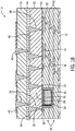
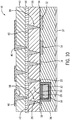
FIGS. 1A and1B are schematic cross-sectional side views of a packaged module according to embodiments of the invention. -
FIGS. 2-10 are schematic cross-sectional side views of a packaged module during various stages of a manufacturing/build-up process according to an embodiment of the invention. -
FIG. 11 is a schematic cross-sectional side view of a packaged module according to another embodiment of the invention. - Embodiments of the invention provide for an embedded dry film battery module having a battery formed therein directly on a dielectric substrate via a dry film sputtering and evaporating technique.
- Referring to
FIGS. 1A and1B , a packagedelectronics module 10 are shown according to embodiments of the invention. The packagedmodules 10 include a number ofelectronic components dry film battery 18. In the illustrated embodiments, thecomponents type sensor 12 and asemiconductor device 14 andcommunications device 16 that collectively form a means for wireless data communication. TheMEMS sensor 12 may be any type of sensing device that is suitable for an intended use of the packagedmodule 10, with a MEMS accelerometer, gas sensor, or electric/magnetic field sensor being examples of such sensors. Thesemiconductor device 14 may be in the form of a die, chip, application specific integrated circuit (ASIC), or processor, for example, and thecommunications device 16 may be in the form of an RF circuit and antenna(s) that might utilize standard wireless communication protocols such as G4, WiFi or Bluetooth, for example. Thus, in one embodiment, thesemiconductor device 14 andcommunications device 16 might collectively form a Bluetooth wireless chip set. While a specific arrangement ofelectronic components FIG. 1 , it is recognized that additional semiconductor devices or electronic components could be included in the packagedmodule 10, and thus embodiments of the invention are not limited to the specific embodiments illustrated inFIGS. 1A and1B . - As shown in
FIGS. 1A and1B , thedry film battery 18 and each ofelectronic components dielectric layer 20 of the packagedmodule 10. According to an exemplary embodiment, thedielectric layer 20 is provided in the form of a lamination or film and is formed of a material that is chosen to provide mechanical and temperature stability to vias during use and frame processing, as well as provide suitable dielectric properties and voltage breakdown strength and processability for via formation and power overly (POL) processing. Accordingly, thedielectric layer 20 may be formed of one a plurality of dielectric materials, such as Kapton®, Ultem®, polytetrafluoroethylene (PTFE), Upilex®, polysulfone materials (e.g., Udel®, Radel®), or another polymer film, such as a liquid crystal polymer (LCP) or a polyimide material, according to embodiments of the invention. - In
FIGS. 1A and1B , it can be seen thatdry film battery 18 is provided directly ontodielectric layer 20. In an exemplary embodiment, thedry film battery 18 is formed directly onto thedielectric layer 20 via a fabrication process described herebelow; however, it is recognized that other embodiments of the invention may be directed to packages where an already fabricatedbattery 18 is placed ontodielectric layer 20. In an embodiment where thedry film battery 18 is formed directly onto thedielectric layer 20, ananode electrode 22 of thebattery 18 is first deposited and defined on thedielectric layer 20 via a sputtering and evaporating technique, a dryfilm electrolyte structure 24 is then deposited onto theanode 22, and acathode electrode 26 is then deposited and defined over the dryfilm electrolyte structure 24. In an exemplary embodiment, thebattery 18 is in the form of a thin film lithium microbattery, and thus fabrication of thebattery 18 includes steps of depositing/defining alithium anode electrode 22 onto thedielectric layer 20, applying a base layer oflithium 28 onto theanode 22, depositing dry film electrolytes of LiPON 30 and LiCoO2 32 onto the base layer oflithium 28, and depositing/defining alithium cathode electrode 26 over the stacked layers ofdry film electrolytes 24. It is recognized, however, thatbattery 18 may be another suitable type of dry film battery besides a lithium battery, and thus embodiments of the invention are not limited only to thin film lithium batteries. - For securing
electronic components dielectric layer 20, an adhesive material 34 (i.e., an "attachment adhesive") is included on the dielectric layer 20 - with theelectronic components adhesive material 34 is also applied over thedry film battery 18 to serve as a protective coating or encapsulant for the battery. An electrically insulatingsubstrate 36 is also provided in packagedmodule 10 and is formed so as to surround theelectronic components battery 18, so as to provide protection thereto and provide additional structural integrity to the packagedmodule 10. In the embodiment illustrated inFIG. 1A , the electricallyinsulating substrate 36 is provided in the form of a dielectric "overmold" encapsulant, such as a polymeric encapsulant or epoxy. However, it is recognized that the electrically insulatingsubstrate 36 could instead be provided in other alternative forms, such as being provided as a multi-layer dielectric construction (i.e., a stack of dielectric layers) applied and formed around thecomponents battery 18, as shown inFIG. 1B , with it being recognized that such a multi-layer dielectric construction would also allow for other routing layers to be formed in such layers and provide an electrical path to the other/back side of the packagedmodule 10. In either embodiment, the electrically insulatingsubstrate 36 is formed to present a level or planar back surface for the packagedmodule 10, and an outeradhesive layer 37 may be applied onto the back side of the electrically insulatingsubstrate 36 to enable "peel and stick" applications for the packagedmodule 10 onto a desired device with which the packagedmodule 10 is to be employed. - As shown in
FIGS. 1A and1B , a plurality ofvias 38 and patternedmetal interconnects 40 are formed in and on thedielectric layer 20. Thevias 38 are formed throughdielectric layer 20 down to a front/active surface of theelectronic components anode 22 and cathode 26 (i.e., terminals) ofdry film battery 18. Metal interconnects 40 are subsequently formed in the packagedmodule 10 to provide electrical connections therein, with theinterconnects 40 being formed in thevias 38 and out onto a surface ofdielectric layer 20. According to embodiments of the invention, the metal interconnects 40 comprise "POL interconnects" that are formed as robust electroplated copper interconnects that form direct electrical connections in thedevice 12. Depending on the metallization on the device, in some embodiments, a sputtered adhesion layer (titanium, chromium, etc.) is provided along with a sputtered copper seed layer on which copper can be plated. As shown inFIG. 1 , the metal interconnects 40 are patterned and etched to a desired shape, such as to provide for electrical connections to packagedmodule 10. - According to one embodiment, an
additional dielectric layer 42 is applied to dielectric layer 20 (by way of an adhesive layer 44). Thus, upon forming of the metal interconnects 40 in/on dielectric layer,additional dielectric layer 42 is added todielectric layer 20.Vias 38 are then subsequently drilled in the addeddielectric layer 42, withmetal interconnects 40 being plated in thevias 38 and patterned on an outer surface of thelayer 42. The dielectric layers 20, 42 serve as redistribution layers that serve to route electrical connections within the packagedmodule 10. While not shown inFIGS. 1A and1B , it is recognized that - in some embodiments - package I/Os can be provided on the topmost redistribution layer (i.e., layer 42), such as in the form of a ball grid array (BGA), to provide a second level connection to a printed circuit board (PCB) or other external device. - In the embodiment, of
FIG. 1B , it is recognized thatvias 38 andmetal interconnects 40 may be formed in/on the stack ofdielectric layers 43 that form the electrically insulatingsubstrate 36 in the same fashion as described above for thevias 38 and interconnects 40 formed indielectric layers interconnects 40 could provide an electrical path to the back side of the packagedmodule 10. - According to one embodiment, antenna structures (not shown) can be formed and routed in the redistribution layers 20, 42 (and/or in dielectric layers 43). The antenna structures can provide enhanced signal reception and transmission from the
communications device 16 included in packagedmodule 10. - A packaged
module 10 is thus provided having abattery 18 integrated therein that is formed on a common substrate (i.e., dielectric layer 20) along with otherelectronic components module 10 is thus in the form of a self-powered module with very low losses and a thin profile. The packagedmodule 10 can be designed to provide a number of functions or sensing applications, such as for IoT applications where the module includes integrated wireless/blue tooth components and antennas for sending real time data/analytics. - Referring now to
FIGS. 2-10 , detailed views of the process steps for a technique of manufacturing a packagedmodule 10 are provided, according to an embodiment of the invention. The technique illustrated inFIGS. 2-10 is shown and described for manufacturing a packagedmodule 10 as shown inFIG. 1 (i.e., including asensor 12, wireless chip set 14, 16, and dry film battery 18), however, it is recognized that the described process is applicable to manufacturing packaged modules that embed sensors, semiconductor devices, and/or communications devices of various configurations. - Referring to
FIG. 2 , the build-up process of packagedmodule 10 begins with the placement and attachment of adielectric layer 20 onto aframe structure 46, with theframe structure 46 being bonded to either side of the dielectric layer, in a roll-to-roll (e.g., "35 mm" strip format with tracks or keep out areas for handling) or frame format, in a manner known in the art. Thedielectric layer 20 is in the form of a lamination or film and is placed onframe structure 46 to provide stability during the build-up process of the packagedmodule 10. According to embodiments of the invention, thedielectric layer 20 may be formed of one a plurality of dielectric materials, such as Kapton®, Ultem®, polytetrafluoroethylene (PTFE), Upilex®, polysulfone materials (e.g., Udel®, Radel®), or another polymer film, such as a liquid crystal polymer (LCP) or a polyimide material. - As shown in
FIG. 3 , upon securing ofdielectric layer 20 to framestructure 46, adry film battery 18 is provided ondielectric layer 20. In an exemplary embodiment, thedry film battery 18 is formed/fabricated directly onto thedielectric layer 20 however, it is recognized that other embodiments of the invention may be directed to packages where an already fabricatedbattery 18 is placed ontodielectric layer 20. In fabricating thebattery 18, in an embodiment where thebattery 18 is in the form of a thin film lithium microbattery, alithium anode electrode 22 is initially deposited onto thedielectric layer 20, such as via a sputtering application. Upon depositing of theanode 22 ontodielectric layer 20, a build-up application of various battery layers is next applied onto the anode 22 - with the build-up application including depositing (e.g., sputtering) of a base layer oflithium 28 , depositing of a dry film electrolyte ofLiPON 30, and depositing of a dry film electrolyte ofLiCoO 2 32. Upon depositing of this described stack of battery layers 28, 30, 32, alithium cathode electrode 26 is then deposited and defined over the stacked layers of dry film electrolytes, with thecathode 26 also extending down a side of thestacked layers dielectric layer 20. It is recognized that the fabrication ofbattery 18 described above may not constitute the full fabrication process and that additional process steps may be required, as would be recognized by one skilled in the art. - Subsequent to forming of the
battery 18 ondielectric layer 20, and as shown inFIG. 4 , anadhesive material 34 is applied onto thedielectric layer 20 on a same side thereof as which dryfilm battery 18 was formed on. In one embodiment, theadhesive material 34 is also applied over thedry film battery 18 to serve as a protective layer or encapsulant for thebattery 18, although it is recognized thatadhesive material 34 need not be applied over the protection (i.e., may rely only on electrically insulatingsubstrate 36 for battery protection). Upon application of the adhesive 34, electronic components, such asMEMS type sensor 12,semiconductor device 14 andcommunications device 16, are then placed and attached face down (i.e., active side down) onto the adhesive 34 to secure the components ontodielectric layer 20, as shown inFIG. 5 . A curing step is then performed to cure the adhesive 34 and secure theelectronic components dielectric layer 20. - In a next step of the build-up process, and as shown in
FIG. 6 , an electrically insulatingsubstrate 36 is applied so as to surround theelectronic components battery 18. In the embodiment illustrated inFIG. 6 , the electrically insulatingsubstrate 36 is applied as a dielectric "overmold" encapsulant, such as a polymeric encapsulant or epoxy. However, as previously explained, the electrically insulatingsubstrate 36 could instead be provided/formed as a stack of dielectric layers. In either embodiment, the electrically insulating substrate36 is formed to present a level or planar back surface for the packagedmodule 10 that enables mounting of the module to a desired device, as will be explained in more detail below. - Referring now to
FIG. 7 , upon over molding and encapsulating theelectronic components battery 18, a plurality ofvias 38 is formed through the dielectric layer 20 (and adhesive layer 34) to theterminals battery 18 and to I/O pads of theelectronic components vias 38 are blind vias formed down to the terminals and I/Os of thebattery 18 andelectronic components vias 38 may be formed by way of a laser ablation or laser drilling process, plasma etching, photo-definition, or mechanical drilling processes. While the formation ofvias 38 throughdielectric layer 20 is shown inFIG. 7 as being performed after attachment ofelectronic components dry film battery 18 ondielectric layer 20, it is recognized that the formation ofvias 38 could be performed prior to placement ofcomponents battery 18 onto dielectric layer 20 (i.e., onto adhesive layer 34). That is, depending on constraints imposed by via size, vias 38 could first be formed indielectric layer 20 prior to attachment ofelectronic components dry film battery 18 ondielectric layer 20, with thevias 38 being formed at locations corresponding to a plurality of terminals and/or connection pads formed on theelectronic components battery 18. Furthermore, a combination of pre- and post- drilled vias could be employed as needed. - Once the
vias 38 have been formed down toterminals battery 18 and to I/O pads of theelectronic components module 10, as shown inFIG. 8 . According to one embodiment, the metal interconnects 40 may be formed through a combination of sputtering and electroplating applications, although it is recognized that other methods of metal deposition (e.g., electroless or electrolytic plating) could also be used. For example, a titanium , TiW or palladium adhesion layer and copper seed layer may first be applied invias 38 by way of a sputtering or electroless plating process, followed by an electroplating process that fills thevias 38 and increases a thickness of (i.e., "plating up") the copper to a desired level. In one embodiment, a patterning and etching is then subsequently performed on the applied copper to forminterconnects 40 having a desired shape. While application of a continuous copper layer and subsequent patterning and etching of the continuous copper layer is described here for forminginterconnects 40, it is recognized that patterning and plating of theinterconnects 40 via a semi-additive plating process could instead be employed to form theinterconnects 40. - According to one embodiment, and as shown in
FIG. 9 , additional routing layers can be applied to packagedmodule 10 in a next step of the build-up process. That is, upon forming of the metal interconnects 40 in packagedmodule 10, one or more additional dielectric layers - such asdielectric layer 42 inFIG. 9 - may be added to the packagedmodule 10, with an adhesive 44 being used to attacheddielectric layer 42 todielectric layer 20. As shown in phantom inFIG. 9 , it is recognized that eachadditional dielectric layer 42 would be mounted on a frame before being added to the previous layer. In one embodiment, thedielectric layer 42 is formed of a material identical to that ofdielectric layer 20, and thus layer may be one a plurality of dielectric materials, such as Kapton®, Ultem®, polytetrafluoroethylene (PTFE), Upilex®, polysulfone materials (e.g., Udel®, Radel®), or another polymer film, such as a liquid crystal polymer (LCP) or a polyimide material.Vias 38 andmetal interconnects 40 are then subsequently formed in/on the addeddielectric layer 42 by way of the via formation and metal interconnect plating/patterning processes described in detail above. Additionally, in an embodiment where the electrically insulatingsubstrate 36 is provided/formed as a stack of dielectric layers (i.e.,dielectric layers 43 inFIG. 1B ), it is recognized thatvias 38 andmetal interconnects 40 could formed in/on the added dielectric layers by way of the via formation and metal interconnect plating/patterning processes previously described. - Upon the addition of any desired additional dielectric layer(s) 42 (and/or layers 43) and the subsequent formation of
vias 38 andmetal interconnects 40 in/on the dielectric layer(s) 42, the packagedmodule 10 is removed from the processing frame orpanel 46, and a final step of the module fabrication process may be performed by applying an outeradhesive layer 37 onto the back side of the electrically insulatingsubstrate 36, as shown inFIG. 10 . Addition of theadhesive layer 37 enables the packagedmodule 10 to be used in "peel and stick" applications - where the packagedmodule 10 may be applied onto a desired device with which the packagedmodule 10 is to be employed. WhileFIG. 10 , illustrates application of theadhesive layer 37 onto the back side of the packagedmodule 10, it is recognized that an adhesive layer could additionally/alternatively be applied onto a side surface of the packagedmodule 10 or the front surface of the packagedmodule 10. - While
FIGS. 1A and1B andFIGS. 2-10 show and describe a packagedmodule 10 where adry film battery 18 is formed/provided in a selected location ondielectric substrate 20 and supported thereby, it is recognized that an alternative embodiment of a packaged module may be formed where a dry film battery is formed as part of an overall substrate of the module. Referring now toFIG. 11 , a packagedmodule 50 is illustrated according to another embodiment. In the embodiment ofFIG. 11 , it can be seen that adry film battery 52 is provided in packagedmodule 50 that forms part of the package substrate. More specifically, adry film battery 52 having a stacked construction similar to previously described - e.g., stacked layers oflithium 54,LiPON 56 andLiCoO 2 58, with lithium anode andcathode electrodes 60, 62 - is formed between a pair of dielectric substrate layers 64, 66 that provide support, protection, and connection redistribution for the packagedmodule 50, with thedry film battery 52 being formed so as to fill an entirety of an area/volume between the pair of dielectric substrate layers 64, 66 and cover a surface of each of the dielectric substrate layers 64, 66. While a lithiumdry cell battery 52 is illustrated inFIG. 11 , it is recognized that other thin film battery materials and layers could be substituted for the specific battery materials/layers illustrated inFIG. 11 , according to additional embodiments of the invention. - With regard to dielectric substrate layers 64, 66, each of the dielectric layers is formed of a material that is chosen to provide mechanical and temperature stability to vias during use and frame processing, as well as provide suitable dielectric properties and voltage breakdown strength and processability for via formation and power overly (POL) processing. Accordingly, the dielectric substrate layers 64, 66 may be formed of one a plurality of dielectric materials, such as Kapton®, Ultem®, polytetrafluoroethylene (PTFE), Upilex®, polysulfone materials (e.g., Udel®, Radel®), mylar, or another polymer film, such as a liquid crystal polymer (LCP) or a polyimide material, according to embodiments of the invention.
- Dielectric substrate layers 64, 66 may include one or more electronic components mounted thereon, such as two
components layer 66, as shown inFIG. 11 . Theelectronic components dry film battery 52 form a self-powered packagedelectronics module 50 that provides a number of functions or sensing applications (e.g., IoT applications). - As shown in
FIG. 11 , each ofelectronic components O connections 76 formed on an outer facing surface ofdielectric substrate layer 64. Forelectronic components components Os 76 are provided by way ofmetal interconnects 78 formed withinvias 80 that extend through thedry film battery 52 and throughdielectric substrate layer 64. With respect to thevias 80 andmetal interconnects 78 formed throughdry film battery 52 anddielectric substrate layer 64, it is recognized thatsuch vias 80 must be formed to electrically isolate/insulate the metal interconnects 78 therein from thebattery 52. Accordingly, the vias include apassivation layer 86 formed along a surface thereof, with the metal interconnects 78 filling-in thevias 80 withinpassivation layer 86 such that the metal interconnects 78 are electrically isolated/insulated from thebattery 52 While not shown inFIG. 11 , it is recognized that, in one embodiment, vias and corresponding interconnects may also be formed down to thebattery 52 to provide for charging the battery, such that packagedmodule 50 may be in the form of a self-sustaining powered module or sensor. - As also shown in
FIG. 11 ,additional metal interconnects 88, 90 are formed to electrically couple theelectronic components cathode electrodes dry film battery 52, such thatbattery 52 may provide power to thesecomponents 68, 70 (i.e., components are power consuming devices, such as semiconductor devices, for example). For the metal interconnects 88 that electrically couple theelectronic components anode 60, such interconnects 88 extend throughvias 92 formed in/through the dry film battery 52 (i.e., throughcathode 62 and layers 54, 56, 58). It is again recognized thatvias 92 must be formed to electrically isolate/insulate the metal interconnects 88 therein from thebattery 52 and thus vias 92 also include apassivation layer 86 formed along a surface thereof, with the metal interconnects 88 filling-in thevias 92 withinpassivation layer 86 such that the metal interconnects 88 are electrically isolated/insulated from thecathode 62 and layers 54, 56, 58. - A packaged
module 50 is thus provided having abattery 52 integrated therein that is formed as part of an overall substrate of the packagedmodule 50. The packagedmodule 50 is thus in the form of a self-powered module with very low losses and a thin profile. The packagedmodule 50 can be designed to provide a number of functions or sensing applications, such as for IoT applications where the module includes integrated wireless/blue tooth components and antennas for sending real time data/analytics. The integratedbattery 18 provides the function of a substrate and can "fill in" all inactive spaces in the package, with it being possible to integrate electronic components on both sides of thebattery 18. - Beneficially, embodiments of the invention thus provide a packaged electronics module having a dry film battery incorporated therein. By incorporating of the battery into the packaged module, a self-powered module is provided that eliminates the need to connect to an externally mounted battery. Incorporation of the battery thus lowers power losses associated with operating the module and provides a thin module having a small form factor. The self-powered packaged electronics module can be manufactured within and as part of the overall package build-up process in a panel format, so as to reduce fabrication costs of the battery and associated module. The self-powered packaged electronics module may provide a number of functions or sensing applications for IoT applications, including the module integrating wireless/Bluetooth components and antennas for sending real time data/analytics, for example. High temperature applications, RF high frequency operation, a flexible/conformal structure, and "peel and stick" applications are still additional benefits provided by the self-powered packaged electronics module. Other envisioned benefits include embodiments of the invention incorporating energy harvesting devices into the packaged electronics module to provide for recharging of the dry film battery so as to provide a self-sustaining powered sensor, such as might be useful in non-serviceable or remote areas.
- Therefore, according to one embodiment of the invention, a packaged electronics module includes a first dielectric layer, at least one electronic component attached to or embedded in the first dielectric layer, a dry film battery formed on the first dielectric layer, and metal interconnects mechanically and electrically coupled to the at least one electronic component and the dry film battery to form electrical interconnections thereto.
- According to another embodiment of the invention, a method of manufacturing a packaged electronics module includes providing a first dielectric layer, forming a dry film battery directly onto the first dielectric layer, attaching one or more electronic components to the first dielectric layer, forming a plurality of vias through the first dielectric layer, and forming metal interconnects in the plurality of vias formed through the first dielectric layer, the metal interconnects forming electrical interconnections to the one or more electronic components and to the dry film battery.
- According to yet another embodiment of the invention, a packaged electronics module includes a dielectric layer having a first surface and a second surface and a plurality of electronic components attached to the dielectric layer on the first surface, the plurality of electronic components including a MEMS type sensor and a communications chip set including a semiconductor device and a communications device. The packaged electronics module also includes a dry film battery attached to the dielectric layer on the first surface and metal interconnects formed in a plurality of vias formed through the dielectric layer and out onto the second surface of the dielectric layer, the metal interconnects being mechanically and electrically coupled to the MEMS type sensor the communications chip set. The packaged electronics module further includes an electrically insulating substrate applied onto the first surface of the dielectric layer and over the MEMS type sensor the communications chip set, so as to embed the MEMS type sensor the communications chip set therein.
- While the invention has been described in detail in connection with only a limited number of embodiments, it should be readily understood that the invention is not limited to such disclosed embodiments. Rather, the invention can be modified to incorporate any number of variations, alterations, substitutions or equivalent arrangements not heretofore described, but which are commensurate with the spirit and scope of the invention. Additionally, while various embodiments of the invention have been described, it is to be understood that aspects of the invention may include only some of the described embodiments. Accordingly, the invention is not to be seen as limited by the foregoing description, but is only limited by the scope of the appended claims.
Claims (15)
- A packaged electronics module (10) comprising:a first dielectric layer (20);at least one electronic component (12, 14, 16) attached to or embedded in the first dielectric layer (20);a dry film battery (18) provided on the first dielectric layer (20); andmetal interconnects (40) mechanically and electrically coupled to the at least one electronic component (12, 14, 16) and the dry film battery (18) to form electrical interconnections thereto.
- The packaged electronics module (10) of claim 1, further comprising an adhesive layer (34) applied onto the first dielectric layer (20) such that the at least one electronic component (12, 14, 16) is attached to the first dielectric layer (20) via the adhesive layer (34).
- The packaged electronics module (10) of claim 2, wherein the adhesive layer (34) is applied over the dry film battery (18) so as to substantially surround the dry film battery (18) and provide a protective coating thereabout.
- The packaged electronics module (10) of any of claims 1 to 3 further comprising an electrically insulating substrate (36) formed over the at least one electronic component (12, 14, 16) and the dry film battery (18) on a first surface of the first dielectric layer (20).
- The packaged electronics module (10) of claim 4, wherein the electrically insulating substrate (36) comprises one of a dielectric overmold encapsulant and a stack of dielectric layers.
- The packaged electronics module (10) of claim 5, further comprising an outer adhesive layer (37) applied onto a back surface of the electrically insulating substrate (36) that is opposite the first dielectric layer (20), the back surface of the electrically insulating substrate (36) comprising a level or planar surface onto which the outer adhesive layer (37) is applied.
- The packaged electronics module (10) of any preceding claim, wherein the dry film battery (18) comprises:an anode (22) formed directly onto the first dielectric layer (20);a stack of battery material layers (24) formed onto the anode (22); anda cathode (26) formed over the stack of battery material layers (24);wherein metal interconnects (40) form electrical interconnections to the anode (22) and the cathode (26).
- The packaged electronics module (10) of any preceding claim, further comprising a plurality of vias (38) formed through the first dielectric layer (20) to the at least one electronic component (12, 14, 16) and the dry film battery (18), the metal interconnects (40) formed in the plurality of vias (38) and out onto a surface of the first dielectric layer (20).
- The packaged electronics module (10) of any preceding claim, wherein the at least one electronic component (12, 14, 16) comprises a plurality of electronic components, the plurality of electronic components including:a microelectromechanical system (MEMS) type sensor (12);a semiconductor device (14); anda communications device (16);wherein the MEMS type sensor (12), semiconductor device (14), and communications device (16) collectively form a means for parameter sensing and wireless data communication.
- The packaged electronics module (10) of any preceding claim, further comprising an antenna structure formed in or on the first dielectric layer (20).
- The packaged electronics module (10) of any preceding claim, further comprising a second dielectric layer (64) positioned such that the dry film battery (52) is sandwiched between the first dielectric layer (66) and the second dielectric layer (64), the dry film battery (52) filling an entirety of a volume between the first and second dielectric layers (66, 64);
wherein a plurality of vias (38) is formed through the dry film battery (18) and the second dielectric layer (42); and
wherein a portion of the metal interconnects (78) is formed in the plurality of vias (80) that extend through the dry film battery (18) and the second dielectric layer (64), with a passivation layer (86) being coated within the plurality of vias (80) to electrically insulate this portion of the metal interconnects (78) from the dry film battery (52). - A method of manufacturing a packaged electronics module (10) comprising:providing a first dielectric layer (20);providing a dry film battery (18) directly on the first dielectric layer (20);attaching one or more electronic components (12, 14, 16) to the first dielectric layer (20);forming a plurality of vias (38) through the first dielectric layer (20); andforming metal interconnects (40) in the plurality of vias (38) formed through the first dielectric layer (20), the metal interconnects (40) forming electrical interconnections to the one or more electronic components (12, 14, 16) and to the dry film battery (18).
- The method of claim 12 further comprising:embedding the one or more electronic components (12, 14, 16) and the dry film battery (18) within an electrically insulating substrate (36), the embedding of the one or more electronic components (12, 14, 16) and the dry film battery (18) comprising one of:over molding the one or more electronic components (12, 14, 16) and the dry film battery (18) with a dielectric encapsulant material; orapplying a stack of dielectric layers over the one or more electronic components (12, 14, 16) and the dry film battery (18); andapplying an outer adhesive layer (37) onto the electrically insulating substrate (36), the outer adhesive layer (37) being applied to a planar back surface of the electrically insulating substrate (36) to provide for a peel and stick application of the packaged electronics module (10) to an external device.
- The method of claim 12, wherein providing the dry film battery (18) comprises forming the dry film battery (18) directly on the first dielectric layer (20), wherein forming the dry film battery (18) further comprises:depositing an anode (22) electrode directly onto the first dielectric layer (20);applying a stack of battery material layers (24) formed onto the anode (22); anddepositing a cathode (26) over the stack of battery material layers (24) and down onto the first dielectric layer (20).
- The method of claim 12 or 13, wherein attaching the one or more electronic components (12, 14, 16) comprises attaching a plurality of electronic components (12, 14, 16), the plurality of electronic components (12, 14, 16) including:a microelectromechanical system (MEMS) type sensor (12);a semiconductor device (14); anda communications device (16);wherein the MEMS type sensor (12), semiconductor device (14), and communications device (16) collectively form an internet of things (IoT) compatible device configured to provide parameter sensing and wireless data communication.
Applications Claiming Priority (1)
| Application Number | Priority Date | Filing Date | Title |
|---|---|---|---|
| US15/209,244 US10660208B2 (en) | 2016-07-13 | 2016-07-13 | Embedded dry film battery module and method of manufacturing thereof |
Publications (1)
| Publication Number | Publication Date |
|---|---|
| EP3270443A1 true EP3270443A1 (en) | 2018-01-17 |
Family
ID=59239766
Family Applications (1)
| Application Number | Title | Priority Date | Filing Date |
|---|---|---|---|
| EP17174808.0A Withdrawn EP3270443A1 (en) | 2016-07-13 | 2017-06-07 | Embedded dry film battery module and method of manufacturing thereof |
Country Status (6)
| Country | Link |
|---|---|
| US (1) | US10660208B2 (en) |
| EP (1) | EP3270443A1 (en) |
| JP (1) | JP7109139B2 (en) |
| KR (1) | KR102353065B1 (en) |
| CN (1) | CN107622988A (en) |
| TW (1) | TWI720218B (en) |
Cited By (1)
| Publication number | Priority date | Publication date | Assignee | Title |
|---|---|---|---|---|
| CN119835865A (en) * | 2023-10-12 | 2025-04-15 | 强茂股份有限公司 | Package element capable of reducing bubble generation and manufacturing method thereof |
Families Citing this family (5)
| Publication number | Priority date | Publication date | Assignee | Title |
|---|---|---|---|---|
| US10044009B2 (en) * | 2016-09-08 | 2018-08-07 | Stmicroelectronics (Tours) Sas | Encapsulated microbattery having terminal connected to active layer through a via |
| WO2018224119A1 (en) * | 2017-06-05 | 2018-12-13 | Telefonaktiebolaget Lm Ericsson (Publ) | Beam mangement systems and methods |
| US20200176377A1 (en) * | 2018-11-30 | 2020-06-04 | Nanya Technology Corporation | Electronic device and method of manufacturing the same |
| CN110060983B (en) * | 2019-05-23 | 2024-06-25 | 盛合晶微半导体(江阴)有限公司 | Antenna packaging structure and packaging method |
| KR102767531B1 (en) * | 2022-08-18 | 2025-02-17 | 오병준 | Formwork panel for easy installation of elbow for water supply pipe and elbow installation method for water supply pipe using the same |
Citations (3)
| Publication number | Priority date | Publication date | Assignee | Title |
|---|---|---|---|---|
| US20100019370A1 (en) * | 2008-07-24 | 2010-01-28 | Infineon Technologies Ag | Semiconductor device and manufacturing method |
| US20150084157A1 (en) * | 2013-09-26 | 2015-03-26 | Infineon Technologies Ag | Electronic structure, a battery structure, and a method for manufacturing an electronic structure |
| EP2916354A2 (en) * | 2014-03-04 | 2015-09-09 | General Electric Company | Ultra-thin embedded semiconductor device package and method of manufacturing thereof |
Family Cites Families (33)
| Publication number | Priority date | Publication date | Assignee | Title |
|---|---|---|---|---|
| JPH01124248A (en) * | 1987-11-09 | 1989-05-17 | Matsushita Electric Ind Co Ltd | Electronic component |
| JPH0364385A (en) * | 1989-08-02 | 1991-03-19 | Kanzaki Paper Mfg Co Ltd | Repeelable pressure-sensitive adhesive sheet |
| US6077106A (en) | 1997-06-05 | 2000-06-20 | Micron Communications, Inc. | Thin profile battery mounting contact for printed circuit boards |
| JPH11354690A (en) * | 1998-06-05 | 1999-12-24 | Mitsubishi Electric Corp | Semiconductor device |
| CN1107356C (en) | 1998-07-08 | 2003-04-30 | 武汉大学 | Method for manufacturing lithium ion battery of plastic film |
| JP4129667B2 (en) | 2000-04-21 | 2008-08-06 | 富士フイルム株式会社 | Battery built-in board |
| WO2002057921A1 (en) | 2001-01-19 | 2002-07-25 | Hitachi,Ltd | Electronic circuit device |
| US8394522B2 (en) | 2002-08-09 | 2013-03-12 | Infinite Power Solutions, Inc. | Robust metal film encapsulation |
| JP4471926B2 (en) * | 2003-05-30 | 2010-06-02 | 株式会社ルネサステクノロジ | Semiconductor device |
| US6986199B2 (en) * | 2003-06-11 | 2006-01-17 | The United States Of America As Represented By The Secretary Of The Navy | Laser-based technique for producing and embedding electrochemical cells and electronic components directly into circuit board materials |
| TWI266445B (en) * | 2004-05-19 | 2006-11-11 | Antig Tech Co Ltd | Battery with embedded electronic circuit |
| US8766435B2 (en) | 2004-06-30 | 2014-07-01 | Stmicroelectronics, Inc. | Integrated circuit package including embedded thin-film battery |
| WO2007131227A2 (en) * | 2006-05-05 | 2007-11-15 | Advanced Cerametrics, Inc. | Self-powered portable electronic device |
| KR20110041964A (en) | 2008-03-21 | 2011-04-22 | 오컴 포트폴리오 엘엘씨 | Solderless electronic assembly and manufacturing method thereof |
| WO2010036784A1 (en) * | 2008-09-26 | 2010-04-01 | Parker Hannifin Corporation | Thermally conductive gel packs |
| IT1392321B1 (en) | 2008-12-15 | 2012-02-24 | St Microelectronics Srl | SENSOR / ACTUATOR SYSTEM ENTIRELY IN ORGANIC MATERIAL |
| TWI423414B (en) * | 2009-02-20 | 2014-01-11 | 國家半導體公司 | Integrated circuit micromodule |
| US8187920B2 (en) * | 2009-02-20 | 2012-05-29 | Texas Instruments Incorporated | Integrated circuit micro-module |
| US7843056B2 (en) * | 2009-02-20 | 2010-11-30 | National Semiconductor Corporation | Integrated circuit micro-module |
| CN102576828B (en) | 2009-09-01 | 2016-04-20 | 萨普拉斯特研究有限责任公司 | Printed circuit board with integrated thin-film battery |
| EP2362421A1 (en) | 2010-02-26 | 2011-08-31 | STMicroelectronics S.r.l. | Tailorable flexible sheet of monolithically fabricated array of separable cells each comprising a wholly organic, integrated circuit adapted to perform a specific function |
| US9224664B2 (en) * | 2012-06-06 | 2015-12-29 | The Charles Stark Draper Laboratory, Inc. | Bio-implantable hermetic integrated ultra high density device |
| JP2014086330A (en) | 2012-10-25 | 2014-05-12 | Fujitsu Ltd | Small-sized power supply module and semiconductor module |
| US9496211B2 (en) | 2012-11-21 | 2016-11-15 | Intel Corporation | Logic die and other components embedded in build-up layers |
| JP2014116368A (en) | 2012-12-06 | 2014-06-26 | Panasonic Corp | Electronic component module and manufacturing method therefor |
| JP6144058B2 (en) * | 2013-01-31 | 2017-06-07 | 新光電気工業株式会社 | Wiring board and method of manufacturing wiring board |
| CN105474406A (en) * | 2013-04-13 | 2016-04-06 | 速力斯公司 | Smart photovoltaic cells and modules |
| US9209151B2 (en) * | 2013-09-26 | 2015-12-08 | General Electric Company | Embedded semiconductor device package and method of manufacturing thereof |
| JP6386746B2 (en) | 2014-02-26 | 2018-09-05 | 株式会社ジェイデバイス | Semiconductor device |
| JP6163702B2 (en) | 2014-12-09 | 2017-07-19 | インテル・コーポレーション | Method for manufacturing package substrate or device |
| FR3039005A1 (en) * | 2015-07-13 | 2017-01-20 | St Microelectronics Tours Sas | AUTOSUPPORTED THIN-FILM BATTERY AND METHOD OF MANUFACTURING SUCH BATTERY |
| US10014710B2 (en) * | 2015-12-09 | 2018-07-03 | Intel Corporation | Foldable fabric-based packaging solution |
| US10044009B2 (en) * | 2016-09-08 | 2018-08-07 | Stmicroelectronics (Tours) Sas | Encapsulated microbattery having terminal connected to active layer through a via |
-
2016
- 2016-07-13 US US15/209,244 patent/US10660208B2/en active Active
-
2017
- 2017-06-07 EP EP17174808.0A patent/EP3270443A1/en not_active Withdrawn
- 2017-06-27 JP JP2017124715A patent/JP7109139B2/en not_active Expired - Fee Related
- 2017-06-29 TW TW106121824A patent/TWI720218B/en active
- 2017-07-13 KR KR1020170089208A patent/KR102353065B1/en active Active
- 2017-07-13 CN CN201710570572.7A patent/CN107622988A/en active Pending
Patent Citations (3)
| Publication number | Priority date | Publication date | Assignee | Title |
|---|---|---|---|---|
| US20100019370A1 (en) * | 2008-07-24 | 2010-01-28 | Infineon Technologies Ag | Semiconductor device and manufacturing method |
| US20150084157A1 (en) * | 2013-09-26 | 2015-03-26 | Infineon Technologies Ag | Electronic structure, a battery structure, and a method for manufacturing an electronic structure |
| EP2916354A2 (en) * | 2014-03-04 | 2015-09-09 | General Electric Company | Ultra-thin embedded semiconductor device package and method of manufacturing thereof |
Cited By (2)
| Publication number | Priority date | Publication date | Assignee | Title |
|---|---|---|---|---|
| CN119835865A (en) * | 2023-10-12 | 2025-04-15 | 强茂股份有限公司 | Package element capable of reducing bubble generation and manufacturing method thereof |
| CN119835865B (en) * | 2023-10-12 | 2025-11-04 | 强茂股份有限公司 | Encapsulated components and their manufacturing methods that can reduce bubble formation |
Also Published As
| Publication number | Publication date |
|---|---|
| TWI720218B (en) | 2021-03-01 |
| JP7109139B2 (en) | 2022-07-29 |
| JP2018011052A (en) | 2018-01-18 |
| KR20180007701A (en) | 2018-01-23 |
| US10660208B2 (en) | 2020-05-19 |
| US20180020548A1 (en) | 2018-01-18 |
| KR102353065B1 (en) | 2022-01-19 |
| TW201816960A (en) | 2018-05-01 |
| CN107622988A (en) | 2018-01-23 |
Similar Documents
| Publication | Publication Date | Title |
|---|---|---|
| EP3270443A1 (en) | Embedded dry film battery module and method of manufacturing thereof | |
| US9056760B2 (en) | Miniaturized electrical component comprising an MEMS and an ASIC and production method | |
| US11178772B2 (en) | Component carrier connected with a separate tilted component carrier for short electric connection | |
| JP6342120B2 (en) | Ultra-thin buried die module and manufacturing method thereof | |
| EP3582593B1 (en) | Method of manufacturing a component carrier with a stepped cavity and a stepped component assembly being embedded within the stepped cavity | |
| US11058007B2 (en) | Component carrier with two component carrier portions and a component being embedded in a blind opening of one of the component carrier portions | |
| EP3384529B1 (en) | Electronic device with a plurality of component carrier packages being electrically and mechanically connected electronic device having an integral electromagnetic shielding structure entirely surrounding the electronic device for providing hermetic shielding | |
| US8163596B2 (en) | Stackable electronic package and method of making same | |
| CN107786183A (en) | Embedded RF filter packages structure and its manufacture method | |
| JP2013243345A5 (en) | ||
| US20100244225A1 (en) | Stackable electronic pagkage and method of fabricating same | |
| EP4170712A2 (en) | Electronic assembly and electronic system with impedance matched interconnect structures | |
| CN113013125A (en) | Component carrier with embedded insert laterally between electrically conductive structures of a stack | |
| CN110391194A (en) | Encapsulation integrated circuit with interpolation functions and the method for manufacturing this encapsulation integrated circuit | |
| JP6144058B2 (en) | Wiring board and method of manufacturing wiring board | |
| KR20170002830A (en) | Electronic component module and manufacturing method threrof | |
| US10249859B2 (en) | Battery built-in board and method for manufacturing the same | |
| CN106658967B (en) | Component carrier with alternating vertically stacked layer structure of different charge density | |
| US11410965B2 (en) | Electronic device with embedded component carrier | |
| CN205755064U (en) | Component carrier | |
| CN205356811U (en) | Electronic device | |
| TWI550792B (en) | Semiconductor device, semiconductor laminated module structure, laminated module structure, and manufacturing method thereof |
Legal Events
| Date | Code | Title | Description |
|---|---|---|---|
| PUAI | Public reference made under article 153(3) epc to a published international application that has entered the european phase |
Free format text: ORIGINAL CODE: 0009012 |
|
| AK | Designated contracting states |
Kind code of ref document: A1 Designated state(s): AL AT BE BG CH CY CZ DE DK EE ES FI FR GB GR HR HU IE IS IT LI LT LU LV MC MK MT NL NO PL PT RO RS SE SI SK SM TR |
|
| AX | Request for extension of the european patent |
Extension state: BA ME |
|
| 17P | Request for examination filed |
Effective date: 20180717 |
|
| RBV | Designated contracting states (corrected) |
Designated state(s): AL AT BE BG CH CY CZ DE DK EE ES FI FR GB GR HR HU IE IS IT LI LT LU LV MC MK MT NL NO PL PT RO RS SE SI SK SM TR |
|
| 17Q | First examination report despatched |
Effective date: 20190131 |
|
| STAA | Information on the status of an ep patent application or granted ep patent |
Free format text: STATUS: THE APPLICATION IS DEEMED TO BE WITHDRAWN |
|
| 18D | Application deemed to be withdrawn |
Effective date: 20191015 |