EP3270256A1 - Noise reduction circuit and associated delta-sigma modulator - Google Patents
Noise reduction circuit and associated delta-sigma modulator Download PDFInfo
- Publication number
- EP3270256A1 EP3270256A1 EP17178615.5A EP17178615A EP3270256A1 EP 3270256 A1 EP3270256 A1 EP 3270256A1 EP 17178615 A EP17178615 A EP 17178615A EP 3270256 A1 EP3270256 A1 EP 3270256A1
- Authority
- EP
- European Patent Office
- Prior art keywords
- circuit
- signal
- transistor
- coupled
- type transistor
- Prior art date
- Legal status (The legal status is an assumption and is not a legal conclusion. Google has not performed a legal analysis and makes no representation as to the accuracy of the status listed.)
- Granted
Links
Images




Classifications
-
- G—PHYSICS
- G05—CONTROLLING; REGULATING
- G05F—SYSTEMS FOR REGULATING ELECTRIC OR MAGNETIC VARIABLES
- G05F3/00—Non-retroactive systems for regulating electric variables by using an uncontrolled element, or an uncontrolled combination of elements, such element or such combination having self-regulating properties
- G05F3/02—Regulating voltage or current
- G05F3/08—Regulating voltage or current wherein the variable is DC
- G05F3/10—Regulating voltage or current wherein the variable is DC using uncontrolled devices with non-linear characteristics
- G05F3/16—Regulating voltage or current wherein the variable is DC using uncontrolled devices with non-linear characteristics being semiconductor devices
- G05F3/20—Regulating voltage or current wherein the variable is DC using uncontrolled devices with non-linear characteristics being semiconductor devices using diode- transistor combinations
- G05F3/26—Current mirrors
- G05F3/262—Current mirrors using field-effect transistors only
-
- H—ELECTRICITY
- H03—ELECTRONIC CIRCUITRY
- H03M—CODING; DECODING; CODE CONVERSION IN GENERAL
- H03M3/00—Conversion of analogue values to or from differential modulation
- H03M3/30—Delta-sigma modulation
- H03M3/322—Continuously compensating for, or preventing, undesired influence of physical parameters
-
- H—ELECTRICITY
- H03—ELECTRONIC CIRCUITRY
- H03F—AMPLIFIERS
- H03F1/00—Details of amplifiers with only discharge tubes, only semiconductor devices or only unspecified devices as amplifying elements
- H03F1/26—Modifications of amplifiers to reduce influence of noise generated by amplifying elements
-
- H—ELECTRICITY
- H03—ELECTRONIC CIRCUITRY
- H03F—AMPLIFIERS
- H03F3/00—Amplifiers with only discharge tubes or only semiconductor devices as amplifying elements
- H03F3/189—High-frequency amplifiers, e.g. radio frequency amplifiers
- H03F3/19—High-frequency amplifiers, e.g. radio frequency amplifiers with semiconductor devices only
- H03F3/193—High-frequency amplifiers, e.g. radio frequency amplifiers with semiconductor devices only with field-effect devices
-
- H—ELECTRICITY
- H03—ELECTRONIC CIRCUITRY
- H03M—CODING; DECODING; CODE CONVERSION IN GENERAL
- H03M3/00—Conversion of analogue values to or from differential modulation
- H03M3/30—Delta-sigma modulation
- H03M3/322—Continuously compensating for, or preventing, undesired influence of physical parameters
- H03M3/368—Continuously compensating for, or preventing, undesired influence of physical parameters of noise other than the quantisation noise already being shaped inherently by delta-sigma modulators
-
- H—ELECTRICITY
- H03—ELECTRONIC CIRCUITRY
- H03M—CODING; DECODING; CODE CONVERSION IN GENERAL
- H03M3/00—Conversion of analogue values to or from differential modulation
- H03M3/30—Delta-sigma modulation
- H03M3/50—Digital/analogue converters using delta-sigma modulation as an intermediate step
-
- H—ELECTRICITY
- H03—ELECTRONIC CIRCUITRY
- H03F—AMPLIFIERS
- H03F2200/00—Indexing scheme relating to amplifiers
- H03F2200/498—A resistor being added in the source circuit of a transistor amplifier stage as degenerating element
-
- H—ELECTRICITY
- H03—ELECTRONIC CIRCUITRY
- H03M—CODING; DECODING; CODE CONVERSION IN GENERAL
- H03M1/00—Analogue/digital conversion; Digital/analogue conversion
-
- H—ELECTRICITY
- H03—ELECTRONIC CIRCUITRY
- H03M—CODING; DECODING; CODE CONVERSION IN GENERAL
- H03M1/00—Analogue/digital conversion; Digital/analogue conversion
- H03M1/12—Analogue/digital converters
-
- H—ELECTRICITY
- H03—ELECTRONIC CIRCUITRY
- H03M—CODING; DECODING; CODE CONVERSION IN GENERAL
- H03M3/00—Conversion of analogue values to or from differential modulation
- H03M3/30—Delta-sigma modulation
-
- H—ELECTRICITY
- H03—ELECTRONIC CIRCUITRY
- H03M—CODING; DECODING; CODE CONVERSION IN GENERAL
- H03M3/00—Conversion of analogue values to or from differential modulation
- H03M3/30—Delta-sigma modulation
- H03M3/39—Structural details of delta-sigma modulators, e.g. incremental delta-sigma modulators
- H03M3/412—Structural details of delta-sigma modulators, e.g. incremental delta-sigma modulators characterised by the number of quantisers and their type and resolution
- H03M3/422—Structural details of delta-sigma modulators, e.g. incremental delta-sigma modulators characterised by the number of quantisers and their type and resolution having one quantiser only
Definitions
- a delta-sigma modulator generally suffers a quantization noise and a digital-to-analog converter (DAC) noise that may worsen the signal quality and circuit efficiency.
- the quantization noise can be reduced by increasing an over-sampling ratio (OSR), quantization bit number or loop filter order.
- OSR over-sampling ratio
- the DAC noise from a bias source cannot be easily cancelled while a large swing input is applied.
- One solution to cancel the DAC noise is to add a bulky resistor-capacitor low-pass filter in the bias path.
- the bulky resistor-capacitor low-pass filter may occupy large chip area and increase the manufacturing cost.
- a circuit includes a transistor, a signal generating circuit and a noise sensing circuit.
- the signal generating circuit is arranged to provide an input signal.
- the noise sensing circuit is coupled to the transistor and the signal generating circuit, and the noise sensing circuit is arranged for receiving the input signal provided by the signal generating circuit to generate an output signal to the transistor, wherein a signal component of the output signal generated by the noise sensing circuit cancels out a signal component of the input signal provided by the signal generating circuit, and the output signal and the input signal have opposite polarities.
- a delta-sigma modulator comprises a receiving circuit, a loop filter, a quantizer and a digital to analog converter.
- the receiving circuit is arranged for receiving a feedback signal and an input signal to generate a summation signal.
- the loop filter comprises a plurality of amplifying stages connected in series and arranged to receive the summation signal to generate a filtered summation signal.
- the quantizer is coupled to the loop filter, and is arranged for generating a digital output signal according to the filtered summation signal.
- the digital to analog converter is coupled to the quantizer and the receiving circuit, and is arranged for performing a digital to analog converting operation upon a signal derived from the digital output signal to generate the feedback signal to the receiving circuit.
- the digital to analog converter comprises a circuit, and the circuit comprises a transistor, a noise sensing circuit and a current mirror.
- the noise sensing circuit is coupled to the transistor and a signal generating circuit, and the noise sensing circuit is arranged for receiving an input signal provided by the signal generating circuit to generate an output signal to the transistor, wherein a signal component of the output signal generated by the noise sensing circuit cancels out a signal component of the input signal provided by the signal generating circuit, and the output signal and the input signal have opposite polarities; and the current mirror is arranged for mirroring a current from the transistor to generate a mirrored current to the receiving circuit.
- FIG. 1 is a diagram illustrating a circuit 100 according to one embodiment of the present invention.
- the circuit 100 comprises a noise sensing circuit 110, a signal generating circuit (in this embodiment, the signal generating circuit is represented by a noisy block 120), a plurality of main circuits 130_1-130_N, a plurality of transistors (PMOS) M0-MN, and a plurality of resistors R0-RN.
- the circuit 100 is used to cancel the noise contributed from the previous stages (e.g. the noisy block 120) and to provide noise-cancelled signals to the following stages (e.g. the main circuits 130_1-130_N).
- the noisy block 120 can be any voltage source or current source with signals and noises, for example, the noisy block 120 may be a bandgap reference voltage generator or a reference current generator.
- the diode-connected transistor M0 is used to receive an input signal (e.g. an input current lin shown in FIG. 1 ), and the transistors M1-MN serve as current mirrors to mirror the input current lin to generate mirrored currents lout1-loutN to the main circuits 130_1-130_N, respectively. Because the input current lin is noisy, the mirrored currents lout1-loutN may also be noisy.
- the noise sensing circuit 110 is arranged to sense the noise component of the input current lin at an input terminal Nin to generate an output signal Vout at an output terminal Nout to a gate electrode of the transistor M0, to cancel or reduce the noise contributed by the noise component of the input current lin.
- the noise at the gate electrode of the transistor M0 can be reduced, thereby the current mirrors (i.e. the transistors M1-MN) can generate the noise-cancelled mirrored currents lout1-loutN, respectively.
- the main circuits 130_1-130_N can be any circuit required to use a current generated according to the input current lin.
- the main circuit 130_1 may be a continuous time delta-sigma modulator, and the mirrored current lout1 flows into an input node of the continuous time delta-sigma modulator.
- the input current lin may be a DC current provided by the noisy block 120, and when the input current lin suddenly has a noise component, the gate electrode of the transistor M0 will directly suffers this noise component. Meanwhile, the noise sensing circuit 110 generates the output signal Vout that has opposite polarity to the noise component of the input current lin (i.e. the phases of the output signal Vout and the noise component are inverted) to the gate electrode of the transistor M0, to cancel the noise component provided by the input current lin.
- the noise sensing circuit 110 can immediately generate an inverted noise component to the gate electrode of the transistor M0, thus the inverted noise component generated by the noise sensing circuit 110 cancels out the noise component provided by the noisy block 120. Therefore, a voltage level of the gate electrodes of the transistors M0-MN may be more stable, without being affected by the noise component of the input signal lin.
- a low-pass filter may not be needed between the current mirrors (i.e. the transistors M1-MN) and the transistor M0, and thus a capacitor connected to the gate electrode of the transistors M0 may not be needed and the chip area can be reduced.
- FIG. 2 is a diagram illustrating the noise sensing circuit 110 according to one embodiment of the present invention.
- the noise sensing circuit 110 comprises a PMOS MP1, an NMOS MN1 and two resistors R NS1 , and R NS2 .
- a gate electrode of the NMOS MN1 serves as the input terminal Nin to receive an input signal Vin (e.g. a voltage-type noise component of input current lin)
- a source electrode of the NMOS MN1 is coupled to a ground voltage via the resistor R NS1
- a drain electrode of the NMOS MN1 serves as the output terminal Nout to generate the output signal Vout.
- a source electrode of the PMOS MP1 is connected to a supply voltage VDD via the resistor R NS2 , and both the gate electrode and the drain electrode of the PMOS MP1 are connected to the drain electrode of the NMOS MN1.
- a ratio between the resistances of the resistors R NS1 and R NS2 can be design to determine a gain of the noise sensing circuit 110. Therefore, the gain can be robust to process, voltage and temperature (PVT) variation.
- the output signal Vout and the input signal Vin have opposite polarities (i.e. the phases are inverted).
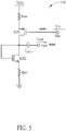
- a capacitor C HPF1 may be positioned between the output terminal Nout and the drain electrode of the NMOS MN1 as shown in FIG. 3 . Hence, the mentioned effect can be eliminated.
- FIG. 4 is a diagram illustrating the noise sensing circuit 110 according to another embodiment of the present invention.
- the noise sensing circuit 110 comprises a PMOS MP2, an NMOS MN2 and two resistors R NS3 and R NS4 .
- a gate electrode of the PMOS MP2 serves as the input terminal Nin to receive the input signal Vin (e.g. a voltage-type noise component of input current lin)
- a source electrode of the PMOS MP2 is coupled to the supply voltage ground voltage via the resistor R NS4
- a drain electrode of the PMOS MP2 serves as the output terminal Nout to generate the output signal Vout.
- a source electrode of the NMOS MN2 is coupled to the ground voltage VDD via the resistor R NS3 , and both the gate electrode and the drain electrode of the NMOS MN2 are coupled to the drain electrode of the PMOS MP2.
- a ratio between the resistances of the resistors R NS3 and R NS4 can be design to determine a gain of the noise sensing circuit 110. Therefore, the gain can be robust to PVT variation.
- the output signal Vout and the input signal Vin have opposite polarities (i.e. the phases are inverted).
- a capacitor C HPF2 may be positioned between the output terminal Nout and the drain electrode of the PMOS MP2 as shown in FIG. 5 . Hence, the mentioned effect can be eliminated.
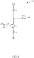
- FIG. 6 is a diagram illustrating the noise sensing circuit 110 according to another embodiment of the present invention.
- the noise sensing circuit 110 comprises an NMOS MN3 and two resistors R NS5 and R NS6 .
- a gate electrode of the NMOS MN3 serves as the input terminal Nin to receive the input signal Vin (e.g. a voltage-type noise component of input current lin)
- a drain electrode of the NMOS MN3 serves as the output terminal Nout to generate the output signal Vout
- a source electrode of the NMOS MN3 is coupled to the ground voltage via the resistor R NS5
- the drain electrode of the NMOS MN3 is coupled to the supply voltage VDD via the resistor R NS6 .
- a resistance of the resistor R NS6 can be designed to make a current flowing through the resistor R NS6 close to the input current lin provided by the noisy block 120 (i.e. the current value of the resistor R NS6 is close to the current value of the input current lin), to prevent the current within the noise sensing circuit 110 from flowing to the external circuit.
- FIG. 7 is a diagram illustrating the noise sensing circuit 110 according to another embodiment of the present invention.
- the noise sensing circuit 110 comprises a PMOS MP3 and two resistors R NS7 and R NS8 .
- a gate electrode of the PMOS MP3 serves as the input terminal Nin to receive the input signal Vin (e.g. a voltage-type noise component of input current lin)
- a drain electrode of the PMOS MP3 serves as the output terminal Nout to generate the output signal Vout
- a source electrode of the PMOS MP3 is coupled to the supply voltage VDD via the resistor R NS8
- the drain electrode of the PMOS MP3 is coupled to the ground voltage via the resistor R NS7 .
- a resistance of the resistor R NS7 can be designed to make a current flowing through the resistor R NS7 close to the input current lin provided by the noisy block 120 (i.e. the current value of the resistor R NS7 is close to the current value of the input current lin), to prevent the current within the noise sensing circuit 110 from flowing to the external circuit.
- the noise sensing circuit 110 is implemented by a single stage amplifier. In other embodiments, however, the noise sensing circuit 110 can be implemented by a multi-stage amplifier, and each stage may be implemented by any one of the embodiments shown in FIGs. 2-7 . This alternative design shall fall within the scope of the present invention.
- FIG. 8 shows a diagram illustrating a circuit 800 according to another embodiment of the present invention.
- the circuit 800 comprises a noise sensing circuit 810, a noisy block 820, a plurality of main circuits 830_1-830_N, a plurality of transistors (NMOS) M0-MN, and a plurality of resistors R0-RN .
- the circuit 800 is used to cancel the noise contributed from the previous stages (e.g. the noisy block 820) and to provide noise-cancelled signals to the following stages (e.g. the main circuits 830_1-830_N).
- FIG. 8 is similar to the embodiment shown in FIG. 1 but the implementations of the transistors M0-MN. That is the operations of the noise sensing circuit 810, the noisy block 820, and main circuits 830_1-830_N are substantially the same as the operations of the noise sensing circuit 110, the noisy block 120, and main circuits 130_1-130_N, respectively. Therefore, further descriptions about the circuit 800 are omitted here.
- FIG. 9 is a diagram illustrating a continuous time delta-sigma modulator 900 according to one embodiment of the present invention.
- the continuous time delta-sigma modulator 900 comprises a receiving circuit 910, a loop filter 920, a quantizer 930, a phase delay/adjusting circuit 940 and a DAC 950.
- the receiving circuit 910 receives an input signal Vi(t) and a feedback signal V FB , and calculates a difference by subtracting the feedback signal V FB by the input signal Vi(t) to generate a summation signal.
- the loop filter 920 is arranged to filter the summation signal to generate a filtered summation signal.
- the quantizer 930 is arranged to generate a digital output Dout according to the filtered residual signal. Then, the digital output Dout is processed by the phase delay/adjusting circuit 940, and the DAC 950 performs a digital-to-analog converting operation upon the signals outputted from the phase delay/adjusting circuit 940 to generate the feedback signal V FB to the receiving circuit 910.
- the DAC 950 comprises a plurality of cells 952, a bias generator 954 and a noise sensing circuit 110/810, where the bias generator 954 receives the input current lin generated from the noisy block 120/820 to generate bias currents to the cells 952 respectively.
- the bias generator 954 may corresponds to the transistors M0-MN shown in FIG. 1 , and each of the cells 952 generates an analog output current or an analog output voltage according to the bias current provided by one of the transistors M1-MN and the digital data outputted by the phase delay/adjusting circuit 940, where a summation of the analog output currents or the analog output voltages of the cells 952 is represented by the feedback signal V FB shown in FIG. 9 .
- V FB shown in FIG. 9 .
- the DAC 950 comprises the noise sensing circuits 110/810 that are applied to the bias generator 954 within the DAC 950 to cancel the noise component of the input current lin provided by the noisy block 120/820 the feedback signal V FB may be cleaner because the noise component contributed by the noisy block 120/820 is cancelled within the DAC 950, that is the DAC noise can be greatly improved.
- a noise reduction loop provided by the noise sensing circuit is applied to cancel the noise from a noisy block, to make the following stages able to receive noise-cancelled signals.
- the noise reduction technique can be applied to a DAC of a delta-sigma modulator to reduce the DAC noise.
Landscapes
- Engineering & Computer Science (AREA)
- Theoretical Computer Science (AREA)
- Microelectronics & Electronic Packaging (AREA)
- Physics & Mathematics (AREA)
- Power Engineering (AREA)
- Nonlinear Science (AREA)
- Electromagnetism (AREA)
- General Physics & Mathematics (AREA)
- Radar, Positioning & Navigation (AREA)
- Automation & Control Theory (AREA)
- Compression, Expansion, Code Conversion, And Decoders (AREA)
- Amplifiers (AREA)
Abstract
Description
- A delta-sigma modulator generally suffers a quantization noise and a digital-to-analog converter (DAC) noise that may worsen the signal quality and circuit efficiency. The quantization noise can be reduced by increasing an over-sampling ratio (OSR), quantization bit number or loop filter order. However, the DAC noise from a bias source cannot be easily cancelled while a large swing input is applied. One solution to cancel the DAC noise is to add a bulky resistor-capacitor low-pass filter in the bias path. However, the bulky resistor-capacitor low-pass filter may occupy large chip area and increase the manufacturing cost.
- It is therefore an objective of the present invention to provide a circuit, which can reduce the circuit noise such as DAC noise without using a low-pass filter, to solve the above-mentioned problem.
- This is achieved by a circuit according to
claim 1 and a delta-sigma modulator according to claim 13. The dependent claims pertain to corresponding further developments and improvements. - As will be seen more clearly from the detailed description following below, a circuit includes a transistor, a signal generating circuit and a noise sensing circuit. The signal generating circuit is arranged to provide an input signal. The noise sensing circuit is coupled to the transistor and the signal generating circuit, and the noise sensing circuit is arranged for receiving the input signal provided by the signal generating circuit to generate an output signal to the transistor, wherein a signal component of the output signal generated by the noise sensing circuit cancels out a signal component of the input signal provided by the signal generating circuit, and the output signal and the input signal have opposite polarities.
- As will be seen more clearly from the detailed description following below, a delta-sigma modulator comprises a receiving circuit, a loop filter, a quantizer and a digital to analog converter. The receiving circuit is arranged for receiving a feedback signal and an input signal to generate a summation signal. The loop filter comprises a plurality of amplifying stages connected in series and arranged to receive the summation signal to generate a filtered summation signal. The quantizer is coupled to the loop filter, and is arranged for generating a digital output signal according to the filtered summation signal. The digital to analog converter is coupled to the quantizer and the receiving circuit, and is arranged for performing a digital to analog converting operation upon a signal derived from the digital output signal to generate the feedback signal to the receiving circuit. The digital to analog converter comprises a circuit, and the circuit comprises a transistor, a noise sensing circuit and a current mirror. The noise sensing circuit is coupled to the transistor and a signal generating circuit, and the noise sensing circuit is arranged for receiving an input signal provided by the signal generating circuit to generate an output signal to the transistor, wherein a signal component of the output signal generated by the noise sensing circuit cancels out a signal component of the input signal provided by the signal generating circuit, and the output signal and the input signal have opposite polarities; and the current mirror is arranged for mirroring a current from the transistor to generate a mirrored current to the receiving circuit.
- These and other objectives of the present invention will no doubt become obvious to those of ordinary skill in the art after reading the following detailed description of the preferred embodiment that is illustrated in the various figures and drawings.
-
-
FIG. 1 is a diagram illustrating a circuit according to one embodiment of the present invention. -
FIG. 2 is a diagram illustrating the noise sensing circuit according to a first embodiment of the present invention. -
FIG. 3 is a diagram illustrating the noise sensing circuit according to a second embodiment of the present invention. -
FIG. 4 is a diagram illustrating the noise sensing circuit according to a third embodiment of the present invention. -
FIG. 5 is a diagram illustrating the noise sensing circuit according to a fourth embodiment of the present invention. -
FIG. 6 is a diagram illustrating the noise sensing circuit according to a fifth embodiment of the present invention. -
FIG. 7 is a diagram illustrating the noise sensing circuit according to a sixth embodiment of the present invention. -
FIG. 8 is a diagram illustrating a circuit according to another embodiment of the present invention. -
FIG. 9 is a diagram illustrating a continuous time delta-sigma modulator according to one embodiment of the present invention. - Certain terms are used throughout the following description and claims to refer to particular system components. As one skilled in the art will appreciate, manufacturers may refer to a component by different names. This document does not intend to distinguish between components that differ in name but not function. In the following discussion and in the claims, the terms "including" and "comprising" are used in an open-ended fashion, and thus should be interpreted to mean "including, but not limited to ..." The terms "couple" and "couples" are intended to mean either an indirect or a direct electrical connection. Thus, if a first device couples to a second device, that connection may be through a direct electrical connection, or through an indirect electrical connection via other devices and connections.
- Please refer to
FIG. 1 , which is a diagram illustrating acircuit 100 according to one embodiment of the present invention. As shown inFIG. 1 , thecircuit 100 comprises anoise sensing circuit 110, a signal generating circuit (in this embodiment, the signal generating circuit is represented by a noisy block 120), a plurality of main circuits 130_1-130_N, a plurality of transistors (PMOS) M0-MN, and a plurality of resistors R0-RN. In this embodiment, thecircuit 100 is used to cancel the noise contributed from the previous stages (e.g. the noisy block 120) and to provide noise-cancelled signals to the following stages (e.g. the main circuits 130_1-130_N). - In the embodiment shown in
FIG. 1 , thenoisy block 120 can be any voltage source or current source with signals and noises, for example, thenoisy block 120 may be a bandgap reference voltage generator or a reference current generator. The diode-connected transistor M0 is used to receive an input signal (e.g. an input current lin shown inFIG. 1 ), and the transistors M1-MN serve as current mirrors to mirror the input current lin to generate mirrored currents lout1-loutN to the main circuits 130_1-130_N, respectively. Because the input current lin is noisy, the mirrored currents lout1-loutN may also be noisy. Therefore, thenoise sensing circuit 110 is arranged to sense the noise component of the input current lin at an input terminal Nin to generate an output signal Vout at an output terminal Nout to a gate electrode of the transistor M0, to cancel or reduce the noise contributed by the noise component of the input current lin. By using thenoise sensing circuit 110, the noise at the gate electrode of the transistor M0 can be reduced, thereby the current mirrors (i.e. the transistors M1-MN) can generate the noise-cancelled mirrored currents lout1-loutN, respectively. - In this embodiment, the main circuits 130_1-130_N can be any circuit required to use a current generated according to the input current lin. For example, the main circuit 130_1 may be a continuous time delta-sigma modulator, and the mirrored current lout1 flows into an input node of the continuous time delta-sigma modulator.
- In detail, the input current lin may be a DC current provided by the
noisy block 120, and when the input current lin suddenly has a noise component, the gate electrode of the transistor M0 will directly suffers this noise component. Meanwhile, thenoise sensing circuit 110 generates the output signal Vout that has opposite polarity to the noise component of the input current lin (i.e. the phases of the output signal Vout and the noise component are inverted) to the gate electrode of the transistor M0, to cancel the noise component provided by the input current lin. In other words, when thenoisy block 120 provides a noise component to the gate electrode of the transistor M0, thenoise sensing circuit 110 can immediately generate an inverted noise component to the gate electrode of the transistor M0, thus the inverted noise component generated by thenoise sensing circuit 110 cancels out the noise component provided by thenoisy block 120. Therefore, a voltage level of the gate electrodes of the transistors M0-MN may be more stable, without being affected by the noise component of the input signal lin. - In addition, in the embodiment shown in
FIG. 1 , since thenoise sensing circuit 110 can reduce the noise from the previous stage to the following stages, a low-pass filter may not be needed between the current mirrors (i.e. the transistors M1-MN) and the transistor M0, and thus a capacitor connected to the gate electrode of the transistors M0 may not be needed and the chip area can be reduced. -
FIG. 2 is a diagram illustrating thenoise sensing circuit 110 according to one embodiment of the present invention. As shown inFIG. 2 , thenoise sensing circuit 110 comprises a PMOS MP1, an NMOS MN1 and two resistors RNS1, and RNS2. A gate electrode of the NMOS MN1 serves as the input terminal Nin to receive an input signal Vin (e.g. a voltage-type noise component of input current lin), a source electrode of the NMOS MN1 is coupled to a ground voltage via the resistor RNS1, and a drain electrode of the NMOS MN1 serves as the output terminal Nout to generate the output signal Vout. A source electrode of the PMOS MP1 is connected to a supply voltage VDD via the resistor RNS2, and both the gate electrode and the drain electrode of the PMOS MP1 are connected to the drain electrode of the NMOS MN1. A ratio between the resistances of the resistors RNS1 and RNS2 can be design to determine a gain of thenoise sensing circuit 110. Therefore, the gain can be robust to process, voltage and temperature (PVT) variation. In this embodiment, the output signal Vout and the input signal Vin have opposite polarities (i.e. the phases are inverted). - To avoid an unwanted effect that a DC level of the drain electrode of the NMOS MN1 affects the gate electrode of the transistor M0, a capacitor CHPF1 may be positioned between the output terminal Nout and the drain electrode of the NMOS MN1 as shown in
FIG. 3 . Hence, the mentioned effect can be eliminated. -
FIG. 4 is a diagram illustrating thenoise sensing circuit 110 according to another embodiment of the present invention. As shown inFIG. 4 , thenoise sensing circuit 110 comprises a PMOS MP2, an NMOS MN2 and two resistors RNS3 and RNS4. A gate electrode of the PMOS MP2 serves as the input terminal Nin to receive the input signal Vin (e.g. a voltage-type noise component of input current lin), a source electrode of the PMOS MP2 is coupled to the supply voltage ground voltage via the resistor RNS4, and a drain electrode of the PMOS MP2 serves as the output terminal Nout to generate the output signal Vout. A source electrode of the NMOS MN2 is coupled to the ground voltage VDD via the resistor RNS3, and both the gate electrode and the drain electrode of the NMOS MN2 are coupled to the drain electrode of the PMOS MP2. A ratio between the resistances of the resistors RNS3 and RNS4 can be design to determine a gain of thenoise sensing circuit 110. Therefore, the gain can be robust to PVT variation. In this embodiment, the output signal Vout and the input signal Vin have opposite polarities (i.e. the phases are inverted). - To avoid an unwanted effect that a DC level of the drain electrode of the PMOS MP2 affects the gate electrode of the transistor M0, a capacitor CHPF2 may be positioned between the output terminal Nout and the drain electrode of the PMOS MP2 as shown in
FIG. 5 . Hence, the mentioned effect can be eliminated. -
FIG. 6 is a diagram illustrating thenoise sensing circuit 110 according to another embodiment of the present invention. As shown inFIG. 6 , thenoise sensing circuit 110 comprises an NMOS MN3 and two resistors RNS5 and RNS6. A gate electrode of the NMOS MN3 serves as the input terminal Nin to receive the input signal Vin (e.g. a voltage-type noise component of input current lin), a drain electrode of the NMOS MN3 serves as the output terminal Nout to generate the output signal Vout, a source electrode of the NMOS MN3 is coupled to the ground voltage via the resistor RNS5, and the drain electrode of the NMOS MN3 is coupled to the supply voltage VDD via the resistor RNS6. In addition, a resistance of the resistor RNS6 can be designed to make a current flowing through the resistor RNS6 close to the input current lin provided by the noisy block 120 (i.e. the current value of the resistor RNS6 is close to the current value of the input current lin), to prevent the current within thenoise sensing circuit 110 from flowing to the external circuit. -
FIG. 7 is a diagram illustrating thenoise sensing circuit 110 according to another embodiment of the present invention. As shown inFIG. 7 , thenoise sensing circuit 110 comprises a PMOS MP3 and two resistors RNS7 and RNS8. A gate electrode of the PMOS MP3 serves as the input terminal Nin to receive the input signal Vin (e.g. a voltage-type noise component of input current lin), a drain electrode of the PMOS MP3 serves as the output terminal Nout to generate the output signal Vout, a source electrode of the PMOS MP3 is coupled to the supply voltage VDD via the resistor RNS8, and the drain electrode of the PMOS MP3 is coupled to the ground voltage via the resistor RNS7. In addition, a resistance of the resistor RNS7 can be designed to make a current flowing through the resistor RNS7 close to the input current lin provided by the noisy block 120 (i.e. the current value of the resistor RNS7 is close to the current value of the input current lin), to prevent the current within thenoise sensing circuit 110 from flowing to the external circuit. - In the embodiments shown in
FIGs. 2-7 , thenoise sensing circuit 110 is implemented by a single stage amplifier. In other embodiments, however, thenoise sensing circuit 110 can be implemented by a multi-stage amplifier, and each stage may be implemented by any one of the embodiments shown inFIGs. 2-7 . This alternative design shall fall within the scope of the present invention. - In the
circuit 100 shown inFIG. 1 , each of the transistors M0-MN are implemented by PMOS. However, the transistors M0-MN may be implemented by NMOSs to achieve the same results.FIG. 8 shows a diagram illustrating acircuit 800 according to another embodiment of the present invention. As shown inFIG. 8 , thecircuit 800 comprises anoise sensing circuit 810, anoisy block 820, a plurality of main circuits 830_1-830_N, a plurality of transistors (NMOS) M0-MN, and a plurality of resistors R0-RN. In this embodiment, thecircuit 800 is used to cancel the noise contributed from the previous stages (e.g. the noisy block 820) and to provide noise-cancelled signals to the following stages (e.g. the main circuits 830_1-830_N). - The embodiment shown in
FIG. 8 is similar to the embodiment shown inFIG. 1 but the implementations of the transistors M0-MN. That is the operations of thenoise sensing circuit 810, thenoisy block 820, and main circuits 830_1-830_N are substantially the same as the operations of thenoise sensing circuit 110, thenoisy block 120, and main circuits 130_1-130_N, respectively. Therefore, further descriptions about thecircuit 800 are omitted here. -
FIG. 9 is a diagram illustrating a continuous time delta-sigma modulator 900 according to one embodiment of the present invention. As shown inFIG. 9 , the continuous time delta-sigma modulator 900 comprises a receivingcircuit 910, aloop filter 920, aquantizer 930, a phase delay/adjusting circuit 940 and aDAC 950. The receivingcircuit 910 receives an input signal Vi(t) and a feedback signal VFB, and calculates a difference by subtracting the feedback signal VFB by the input signal Vi(t) to generate a summation signal. Theloop filter 920 is arranged to filter the summation signal to generate a filtered summation signal. Thequantizer 930 is arranged to generate a digital output Dout according to the filtered residual signal. Then, the digital output Dout is processed by the phase delay/adjusting circuit 940, and theDAC 950 performs a digital-to-analog converting operation upon the signals outputted from the phase delay/adjusting circuit 940 to generate the feedback signal VFB to the receivingcircuit 910. - The
DAC 950 comprises a plurality ofcells 952, abias generator 954 and anoise sensing circuit 110/810, where thebias generator 954 receives the input current lin generated from thenoisy block 120/820 to generate bias currents to thecells 952 respectively. In this embodiment, thebias generator 954 may corresponds to the transistors M0-MN shown inFIG. 1 , and each of thecells 952 generates an analog output current or an analog output voltage according to the bias current provided by one of the transistors M1-MN and the digital data outputted by the phase delay/adjusting circuit 940, where a summation of the analog output currents or the analog output voltages of thecells 952 is represented by the feedback signal VFB shown inFIG. 9 . In the embodiment shown inFIG. 9 because theDAC 950 comprises thenoise sensing circuits 110/810 that are applied to thebias generator 954 within theDAC 950 to cancel the noise component of the input current lin provided by thenoisy block 120/820 the feedback signal VFB may be cleaner because the noise component contributed by thenoisy block 120/820 is cancelled within theDAC 950, that is the DAC noise can be greatly improved. - Briefly summarized, in the noise reduction technique of the present invention, a noise reduction loop provided by the noise sensing circuit is applied to cancel the noise from a noisy block, to make the following stages able to receive noise-cancelled signals. In one embodiment, the noise reduction technique can be applied to a DAC of a delta-sigma modulator to reduce the DAC noise.
- Those skilled in the art will readily observe that numerous modifications and alterations of the device and method may be made while retaining the teachings of the invention. Accordingly, the above disclosure should be construed as limited only by the metes and bounds of the appended claims.
Claims (15)
- A circuit (100, 800), characterized by:a transistor (M0);a signal generating circuit (120, 820), coupled to the transistor (M0), for providing an input signal; anda noise sensing circuit (110, 810), coupled to the transistor (M0) and the signal generating circuit (120, 820), for receiving the input signal provided by the signal generating circuit (120, 820) to generate an output signal to the transistor;wherein a signal component of the output signal generated by the noise sensing circuit (110, 810) cancels out a signal component of the input signal provided by the signal generating circuit (120, 820), and the output signal and the input signal have opposite polarities.
- The circuit (100, 800) of claim 1, characterized in that each of the signal component of the output signal and the signal component of the input signal is a noise component.
- The circuit (100, 800) of claim 1, characterized in that a gate electrode and a drain electrode of the transistor (M0) are coupled to each other, the drain electrode of the transistor (M0) is coupled to the signal generating circuit (120, 820) and an input terminal of the noise sensing circuit (110, 810), and the gate electrode of the transistor (M0) is coupled to an output terminal of the noise sensing circuit (110, 810).
- The circuit (100, 800) of claim 1, characterized in that the noise sensing circuit (110, 810) comprises:an N-type transistor (MN1), wherein a gate electrode of the N-type transistor (MN1) serves as an input terminal to receive the input signal from the signal generating circuit (120, 820), and a drain electrode of the N-type transistor (MN1) is coupled to an output terminal for generating the output signal; anda P-type transistor (MP1), wherein the gate electrode and the drain electrode of the P-type transistor (MP1) are coupled to the drain electrode of the N-type transistor (MN2).
- The circuit (100, 800) of claim 4, characterized in that the noise sensing circuit (110, 810) further comprises:a capacitor (CHPF1), coupled between the output terminal and the drain electrode of the N-type transistor (MN1).
- The circuit (100, 800) of claim 1, characterized in that the noise sensing circuit (110, 810) comprises:a P-type transistor (MP2), wherein a gate electrode of the P-type transistor (MP2) serves as an input terminal to receive the input signal from the signal generating circuit (120, 820), and a drain electrode of the P-type transistor (MP2) is coupled to an output terminal for generating the output signal; andan N-type transistor (MN2), wherein the gate electrode and the drain electrode of the N-type transistor (MN2) are coupled to the drain electrode of the P-type transistor (MP2).
- The circuit (100, 800) of claim 6, characterized in that the noise sensing circuit (110, 810) further comprises:a capacitor (CHPF2), coupled between the output terminal and the drain electrode of the P-type transistor (MP2).
- The circuit (100, 800) of claim 1, characterized in that the noise sensing circuit (110, 810) comprises:an N-type transistor (MN3), wherein a gate electrode of the N-type transistor (MN3) serves as an input terminal to receive the input signal from the signal generating circuit (120, 820), and a drain electrode of the N-type transistor (MN3) serves as an output terminal for generating the output signal;a first resistor (RNS5), coupled between a ground voltage and a source electrode of the N-type transistor (MN3); anda second resistor (RNS6), coupled between a supply voltage (VDD) and the drain electrode of the N-type transistor (MN3).
- The circuit (100, 800) of claim 1, characterized in that the noise sensing circuit (110, 810) comprises:a P-type transistor (MP3), wherein a gate electrode of the P-type transistor (MP3) serves as an input terminal to receive the input signal from the signal generating circuit (120, 820), and a drain electrode of the P-type transistor (MP3) serves as an output terminal for generating the output signal;a first resistor (RNS7), coupled between a ground voltage and the drain electrode of the P-type transistor (MP3); anda second resistor (RNS8), coupled between a supply voltage and a source electrode of the P-type transistor (MP3).
- The circuit (100, 800) of claim 1, characterized in that the circuit (100, 800) further comprises:a current mirror (M1-MN), coupled to the transistor (M0), for mirroring a current from the transistor (M0) to generate a mirrored current to a main circuit (900);wherein there is no low-pass filter positioned between the current mirror (M1 -MN) and the transistor (M0).
- The circuit (100, 800) of claim 10, characterized in that the current mirror (M1-MN) comprises another transistor (M1-MN) whose gate electrode is connected to the gate electrode of the transistor (M0), and the noise sensing circuit (110, 810) generates the output signal to the gate electrode of the transistor (110, 810) to cancel or reduce a noise level caused by the input signal provided by the signal generating circuit (120, 820).
- The circuit (100, 800) of claim 10, characterized in that the main circuit (900) is a delta-sigma modulator, and the mirrored current flows into an input terminal of the delta-sigma modulator (900).
- A delta-sigma modulator (900), comprising:a receiving circuit (910), for receiving a feedback signal and an input signal to generate a summation signal;a loop filter (920) comprising a plurality of amplifying stages connected in series and arranged to receive the summation signal to generate a filtered summation signal;a quantizer (930), coupled to the loop filter, for generating a digital output signal according to the filtered summation signal; anda digital to analog converter (950), coupled to the quantizer (930) and the receiving circuit (910), for performing a digital to analog converting operation upon a signal derived from the digital output signal to generate the feedback signal to the receiving circuit (910); andcharacterized by: the digital to analog converter (950) comprises a circuit, and the circuit comprises:a transistor (M0, 954);a noise sensing circuit (110, 810), coupled to the transistor (M0, 954) and a signal generating circuit (120, 820), for receiving an input signal provided by the signal generating circuit (120, 820) to generate an output signal to the transistor (M0, 954), wherein a signal component of the output signal generated by the noise sensing circuit (110, 810) cancels out a signal component of the input signal provided by the signal generating circuit (120, 820), and the output signal and the input signal have opposite polarities; anda current mirror (M1-MN, 954), coupled to the transistor (M0, 954), for mirroring a current from the transistor (M0, 954) to generate a mirrored current to the receiving circuit (910).
- The delta-sigma modulator (900) of claim 13, characterized in that each of the signal component of the output signal and the signal component of the input signal is a noise component.
- The delta-sigma modulator (900) of claim 13, characterized in that a gate electrode and a drain electrode of the transistor (M0) are coupled to each other, the drain electrode of the transistor (M0) is coupled to the signal generating circuit (120, 820) and an input terminal of the noise sensing circuit (110, 810), and the gate electrode of the transistor (M0) is coupled to an output terminal of the noise sensing circuit (110, 810).
Applications Claiming Priority (2)
| Application Number | Priority Date | Filing Date | Title |
|---|---|---|---|
| US201662360986P | 2016-07-12 | 2016-07-12 | |
| US15/629,731 US9831892B1 (en) | 2016-07-12 | 2017-06-21 | Noise reduction circuit and associated delta-sigma modulator |
Publications (2)
| Publication Number | Publication Date |
|---|---|
| EP3270256A1 true EP3270256A1 (en) | 2018-01-17 |
| EP3270256B1 EP3270256B1 (en) | 2021-08-04 |
Family
ID=60408933
Family Applications (1)
| Application Number | Title | Priority Date | Filing Date |
|---|---|---|---|
| EP17178615.5A Active EP3270256B1 (en) | 2016-07-12 | 2017-06-29 | Noise reduction circuit and associated delta-sigma modulator |
Country Status (4)
| Country | Link |
|---|---|
| US (1) | US9831892B1 (en) |
| EP (1) | EP3270256B1 (en) |
| CN (1) | CN107612551B (en) |
| TW (1) | TWI636671B (en) |
Families Citing this family (5)
| Publication number | Priority date | Publication date | Assignee | Title |
|---|---|---|---|---|
| KR102816303B1 (en) | 2020-04-28 | 2025-06-02 | 삼성전자주식회사 | Noise filtering and electric circuit comprising the same |
| CN113328632B (en) * | 2021-05-08 | 2022-05-06 | 南京君海数能科技有限公司 | Method, apparatus and medium for detecting and suppressing AC link DC bias current |
| JP7752996B2 (en) * | 2021-08-20 | 2025-10-14 | キリンホールディングス株式会社 | Taste presentation device |
| KR102920741B1 (en) * | 2021-12-10 | 2026-01-29 | 삼성전자주식회사 | Noise filtering circuit, digital analog converter and electronic device including the same |
| WO2025080347A1 (en) * | 2023-10-12 | 2025-04-17 | Qorvo Us, Inc. | Systems and methods for noise reduction for multi-stage power amplifier chain |
Citations (2)
| Publication number | Priority date | Publication date | Assignee | Title |
|---|---|---|---|---|
| US4866399A (en) * | 1988-10-24 | 1989-09-12 | Delco Electronics Corporation | Noise immune current mirror |
| US20140247035A1 (en) * | 2013-03-04 | 2014-09-04 | Stmicroelectronics International N.V. | Noise canceling current mirror circuit for improved psr |
Family Cites Families (7)
| Publication number | Priority date | Publication date | Assignee | Title |
|---|---|---|---|---|
| US3462698A (en) * | 1967-02-14 | 1969-08-19 | Gen Electric | All npn transistor dc amplifier |
| JP3484050B2 (en) * | 1997-08-28 | 2004-01-06 | 株式会社日立製作所 | Current mirror circuit |
| EP1402640A1 (en) * | 2001-06-20 | 2004-03-31 | Koninklijke Philips Electronics N.V. | Input pad with improved noise immunity and output characteristics |
| CN101364807B (en) * | 2007-08-10 | 2011-08-24 | 晨星半导体股份有限公司 | Delta-sigma modulator and related methods |
| US9231614B2 (en) * | 2014-04-07 | 2016-01-05 | Analog Devices, Inc. | Cancellation of feedback digital-to-analog converter errors in multi-stage delta-sigma analog-to-digital converters |
| US9276792B1 (en) * | 2014-09-20 | 2016-03-01 | Stiching Vour de Technische Wetenschappen | Phase-domain digitizer |
| US10212006B2 (en) | 2016-03-01 | 2019-02-19 | Mediatek Inc. | Feed-forward filtering device and associated method |
-
2017
- 2017-06-21 US US15/629,731 patent/US9831892B1/en active Active
- 2017-06-29 EP EP17178615.5A patent/EP3270256B1/en active Active
- 2017-07-06 CN CN201710545553.9A patent/CN107612551B/en active Active
- 2017-07-11 TW TW106123176A patent/TWI636671B/en not_active IP Right Cessation
Patent Citations (2)
| Publication number | Priority date | Publication date | Assignee | Title |
|---|---|---|---|---|
| US4866399A (en) * | 1988-10-24 | 1989-09-12 | Delco Electronics Corporation | Noise immune current mirror |
| US20140247035A1 (en) * | 2013-03-04 | 2014-09-04 | Stmicroelectronics International N.V. | Noise canceling current mirror circuit for improved psr |
Also Published As
| Publication number | Publication date |
|---|---|
| CN107612551A (en) | 2018-01-19 |
| US9831892B1 (en) | 2017-11-28 |
| EP3270256B1 (en) | 2021-08-04 |
| CN107612551B (en) | 2021-01-22 |
| TWI636671B (en) | 2018-09-21 |
| TW201803275A (en) | 2018-01-16 |
Similar Documents
| Publication | Publication Date | Title |
|---|---|---|
| EP3270256B1 (en) | Noise reduction circuit and associated delta-sigma modulator | |
| US7906976B2 (en) | Switched capacitor measurement circuit for measuring the capacitance of an input capacitor | |
| EP2128633B1 (en) | Current-sense amplifier arrangement and method for measuring a voltage signal | |
| US9847763B2 (en) | Self-regulated reference for switched capacitor circuit | |
| US8854136B2 (en) | Fully differential operational amplifier with common-mode feedback circuit | |
| KR100825769B1 (en) | On-chip reference current generator and reference voltage generator | |
| US7312657B2 (en) | Class D amplifier | |
| CN113765489A (en) | Chopper amplifier with tracking of multiple input offsets | |
| US6538513B2 (en) | Common mode output current control circuit and method | |
| CN107171650B (en) | Variable gain amplifier circuit | |
| EP3214760A2 (en) | Feed-forward filtering device and associated method | |
| JP2017208634A (en) | OP amplifier and electronic circuit | |
| KR100767581B1 (en) | Differential type operational amplifier | |
| JP2004304632A (en) | Power-on detector and power-on reset circuit using the power-on detector | |
| KR101939147B1 (en) | Variable Voltage Reference Generator and Analog-to-Digital Converter using thereof | |
| KR101920936B1 (en) | Differential amplifier and analog/digital converter | |
| US20160241222A1 (en) | Comparison circuit | |
| JP7438694B2 (en) | amplifier circuit | |
| US12489398B2 (en) | Operation point stabilization for VCO-ADC using switched-capacitor frequency-to-current conversion | |
| US12580527B2 (en) | Reducing sampled AZ noise and sampled reset noise in switched capacitor amplifiers | |
| CN113556103B (en) | Comparison circuit and comparison module with hysteresis function | |
| TWI573391B (en) | Variable gain amplifying circuit | |
| JP2018182357A (en) | Current detection amplifier | |
| KR101390303B1 (en) | Apparatus for differential to single ended converter | |
| CN120315512A (en) | Linear Regulators |
Legal Events
| Date | Code | Title | Description |
|---|---|---|---|
| PUAI | Public reference made under article 153(3) epc to a published international application that has entered the european phase |
Free format text: ORIGINAL CODE: 0009012 |
|
| STAA | Information on the status of an ep patent application or granted ep patent |
Free format text: STATUS: THE APPLICATION HAS BEEN PUBLISHED |
|
| AK | Designated contracting states |
Kind code of ref document: A1 Designated state(s): AL AT BE BG CH CY CZ DE DK EE ES FI FR GB GR HR HU IE IS IT LI LT LU LV MC MK MT NL NO PL PT RO RS SE SI SK SM TR |
|
| AX | Request for extension of the european patent |
Extension state: BA ME |
|
| STAA | Information on the status of an ep patent application or granted ep patent |
Free format text: STATUS: REQUEST FOR EXAMINATION WAS MADE |
|
| 17P | Request for examination filed |
Effective date: 20180709 |
|
| RBV | Designated contracting states (corrected) |
Designated state(s): AL AT BE BG CH CY CZ DE DK EE ES FI FR GB GR HR HU IE IS IT LI LT LU LV MC MK MT NL NO PL PT RO RS SE SI SK SM TR |
|
| STAA | Information on the status of an ep patent application or granted ep patent |
Free format text: STATUS: EXAMINATION IS IN PROGRESS |
|
| 17Q | First examination report despatched |
Effective date: 20200430 |
|
| GRAP | Despatch of communication of intention to grant a patent |
Free format text: ORIGINAL CODE: EPIDOSNIGR1 |
|
| STAA | Information on the status of an ep patent application or granted ep patent |
Free format text: STATUS: GRANT OF PATENT IS INTENDED |
|
| INTG | Intention to grant announced |
Effective date: 20210223 |
|
| RIN1 | Information on inventor provided before grant (corrected) |
Inventor name: TSAI, HUNG-CHIEH |
|
| GRAS | Grant fee paid |
Free format text: ORIGINAL CODE: EPIDOSNIGR3 |
|
| GRAA | (expected) grant |
Free format text: ORIGINAL CODE: 0009210 |
|
| STAA | Information on the status of an ep patent application or granted ep patent |
Free format text: STATUS: THE PATENT HAS BEEN GRANTED |
|
| RIN1 | Information on inventor provided before grant (corrected) |
Inventor name: TSAI, HUNG-CHIEH |
|
| AK | Designated contracting states |
Kind code of ref document: B1 Designated state(s): AL AT BE BG CH CY CZ DE DK EE ES FI FR GB GR HR HU IE IS IT LI LT LU LV MC MK MT NL NO PL PT RO RS SE SI SK SM TR |
|
| REG | Reference to a national code |
Ref country code: GB Ref legal event code: FG4D |
|
| REG | Reference to a national code |
Ref country code: AT Ref legal event code: REF Ref document number: 1417630 Country of ref document: AT Kind code of ref document: T Effective date: 20210815 |
|
| REG | Reference to a national code |
Ref country code: CH Ref legal event code: EP |
|
| REG | Reference to a national code |
Ref country code: DE Ref legal event code: R096 Ref document number: 602017043236 Country of ref document: DE |
|
| REG | Reference to a national code |
Ref country code: IE Ref legal event code: FG4D |
|
| REG | Reference to a national code |
Ref country code: LT Ref legal event code: MG9D |
|
| REG | Reference to a national code |
Ref country code: NL Ref legal event code: MP Effective date: 20210804 |
|
| REG | Reference to a national code |
Ref country code: AT Ref legal event code: MK05 Ref document number: 1417630 Country of ref document: AT Kind code of ref document: T Effective date: 20210804 |
|
| PG25 | Lapsed in a contracting state [announced via postgrant information from national office to epo] |
Ref country code: RS Free format text: LAPSE BECAUSE OF FAILURE TO SUBMIT A TRANSLATION OF THE DESCRIPTION OR TO PAY THE FEE WITHIN THE PRESCRIBED TIME-LIMIT Effective date: 20210804 Ref country code: SE Free format text: LAPSE BECAUSE OF FAILURE TO SUBMIT A TRANSLATION OF THE DESCRIPTION OR TO PAY THE FEE WITHIN THE PRESCRIBED TIME-LIMIT Effective date: 20210804 Ref country code: BG Free format text: LAPSE BECAUSE OF FAILURE TO SUBMIT A TRANSLATION OF THE DESCRIPTION OR TO PAY THE FEE WITHIN THE PRESCRIBED TIME-LIMIT Effective date: 20211104 Ref country code: AT Free format text: LAPSE BECAUSE OF FAILURE TO SUBMIT A TRANSLATION OF THE DESCRIPTION OR TO PAY THE FEE WITHIN THE PRESCRIBED TIME-LIMIT Effective date: 20210804 Ref country code: LT Free format text: LAPSE BECAUSE OF FAILURE TO SUBMIT A TRANSLATION OF THE DESCRIPTION OR TO PAY THE FEE WITHIN THE PRESCRIBED TIME-LIMIT Effective date: 20210804 Ref country code: ES Free format text: LAPSE BECAUSE OF FAILURE TO SUBMIT A TRANSLATION OF THE DESCRIPTION OR TO PAY THE FEE WITHIN THE PRESCRIBED TIME-LIMIT Effective date: 20210804 Ref country code: FI Free format text: LAPSE BECAUSE OF FAILURE TO SUBMIT A TRANSLATION OF THE DESCRIPTION OR TO PAY THE FEE WITHIN THE PRESCRIBED TIME-LIMIT Effective date: 20210804 Ref country code: HR Free format text: LAPSE BECAUSE OF FAILURE TO SUBMIT A TRANSLATION OF THE DESCRIPTION OR TO PAY THE FEE WITHIN THE PRESCRIBED TIME-LIMIT Effective date: 20210804 Ref country code: NO Free format text: LAPSE BECAUSE OF FAILURE TO SUBMIT A TRANSLATION OF THE DESCRIPTION OR TO PAY THE FEE WITHIN THE PRESCRIBED TIME-LIMIT Effective date: 20211104 Ref country code: PT Free format text: LAPSE BECAUSE OF FAILURE TO SUBMIT A TRANSLATION OF THE DESCRIPTION OR TO PAY THE FEE WITHIN THE PRESCRIBED TIME-LIMIT Effective date: 20211206 |
|
| PG25 | Lapsed in a contracting state [announced via postgrant information from national office to epo] |
Ref country code: PL Free format text: LAPSE BECAUSE OF FAILURE TO SUBMIT A TRANSLATION OF THE DESCRIPTION OR TO PAY THE FEE WITHIN THE PRESCRIBED TIME-LIMIT Effective date: 20210804 Ref country code: LV Free format text: LAPSE BECAUSE OF FAILURE TO SUBMIT A TRANSLATION OF THE DESCRIPTION OR TO PAY THE FEE WITHIN THE PRESCRIBED TIME-LIMIT Effective date: 20210804 Ref country code: GR Free format text: LAPSE BECAUSE OF FAILURE TO SUBMIT A TRANSLATION OF THE DESCRIPTION OR TO PAY THE FEE WITHIN THE PRESCRIBED TIME-LIMIT Effective date: 20211105 |
|
| PG25 | Lapsed in a contracting state [announced via postgrant information from national office to epo] |
Ref country code: NL Free format text: LAPSE BECAUSE OF FAILURE TO SUBMIT A TRANSLATION OF THE DESCRIPTION OR TO PAY THE FEE WITHIN THE PRESCRIBED TIME-LIMIT Effective date: 20210804 |
|
| PG25 | Lapsed in a contracting state [announced via postgrant information from national office to epo] |
Ref country code: DK Free format text: LAPSE BECAUSE OF FAILURE TO SUBMIT A TRANSLATION OF THE DESCRIPTION OR TO PAY THE FEE WITHIN THE PRESCRIBED TIME-LIMIT Effective date: 20210804 |
|
| REG | Reference to a national code |
Ref country code: DE Ref legal event code: R097 Ref document number: 602017043236 Country of ref document: DE |
|
| PG25 | Lapsed in a contracting state [announced via postgrant information from national office to epo] |
Ref country code: SM Free format text: LAPSE BECAUSE OF FAILURE TO SUBMIT A TRANSLATION OF THE DESCRIPTION OR TO PAY THE FEE WITHIN THE PRESCRIBED TIME-LIMIT Effective date: 20210804 Ref country code: SK Free format text: LAPSE BECAUSE OF FAILURE TO SUBMIT A TRANSLATION OF THE DESCRIPTION OR TO PAY THE FEE WITHIN THE PRESCRIBED TIME-LIMIT Effective date: 20210804 Ref country code: RO Free format text: LAPSE BECAUSE OF FAILURE TO SUBMIT A TRANSLATION OF THE DESCRIPTION OR TO PAY THE FEE WITHIN THE PRESCRIBED TIME-LIMIT Effective date: 20210804 Ref country code: EE Free format text: LAPSE BECAUSE OF FAILURE TO SUBMIT A TRANSLATION OF THE DESCRIPTION OR TO PAY THE FEE WITHIN THE PRESCRIBED TIME-LIMIT Effective date: 20210804 Ref country code: CZ Free format text: LAPSE BECAUSE OF FAILURE TO SUBMIT A TRANSLATION OF THE DESCRIPTION OR TO PAY THE FEE WITHIN THE PRESCRIBED TIME-LIMIT Effective date: 20210804 Ref country code: AL Free format text: LAPSE BECAUSE OF FAILURE TO SUBMIT A TRANSLATION OF THE DESCRIPTION OR TO PAY THE FEE WITHIN THE PRESCRIBED TIME-LIMIT Effective date: 20210804 |
|
| PLBE | No opposition filed within time limit |
Free format text: ORIGINAL CODE: 0009261 |
|
| STAA | Information on the status of an ep patent application or granted ep patent |
Free format text: STATUS: NO OPPOSITION FILED WITHIN TIME LIMIT |
|
| 26N | No opposition filed |
Effective date: 20220506 |
|
| PG25 | Lapsed in a contracting state [announced via postgrant information from national office to epo] |
Ref country code: IT Free format text: LAPSE BECAUSE OF FAILURE TO SUBMIT A TRANSLATION OF THE DESCRIPTION OR TO PAY THE FEE WITHIN THE PRESCRIBED TIME-LIMIT Effective date: 20210804 |
|
| PG25 | Lapsed in a contracting state [announced via postgrant information from national office to epo] |
Ref country code: SI Free format text: LAPSE BECAUSE OF FAILURE TO SUBMIT A TRANSLATION OF THE DESCRIPTION OR TO PAY THE FEE WITHIN THE PRESCRIBED TIME-LIMIT Effective date: 20210804 |
|
| PG25 | Lapsed in a contracting state [announced via postgrant information from national office to epo] |
Ref country code: MC Free format text: LAPSE BECAUSE OF FAILURE TO SUBMIT A TRANSLATION OF THE DESCRIPTION OR TO PAY THE FEE WITHIN THE PRESCRIBED TIME-LIMIT Effective date: 20210804 |
|
| REG | Reference to a national code |
Ref country code: CH Ref legal event code: PL |
|
| REG | Reference to a national code |
Ref country code: BE Ref legal event code: MM Effective date: 20220630 |
|
| PG25 | Lapsed in a contracting state [announced via postgrant information from national office to epo] |
Ref country code: LU Free format text: LAPSE BECAUSE OF NON-PAYMENT OF DUE FEES Effective date: 20220629 Ref country code: LI Free format text: LAPSE BECAUSE OF NON-PAYMENT OF DUE FEES Effective date: 20220630 Ref country code: IE Free format text: LAPSE BECAUSE OF NON-PAYMENT OF DUE FEES Effective date: 20220629 Ref country code: CH Free format text: LAPSE BECAUSE OF NON-PAYMENT OF DUE FEES Effective date: 20220630 |
|
| PG25 | Lapsed in a contracting state [announced via postgrant information from national office to epo] |
Ref country code: BE Free format text: LAPSE BECAUSE OF NON-PAYMENT OF DUE FEES Effective date: 20220630 |
|
| P01 | Opt-out of the competence of the unified patent court (upc) registered |
Effective date: 20230607 |
|
| PG25 | Lapsed in a contracting state [announced via postgrant information from national office to epo] |
Ref country code: HU Free format text: LAPSE BECAUSE OF FAILURE TO SUBMIT A TRANSLATION OF THE DESCRIPTION OR TO PAY THE FEE WITHIN THE PRESCRIBED TIME-LIMIT; INVALID AB INITIO Effective date: 20170629 |
|
| PG25 | Lapsed in a contracting state [announced via postgrant information from national office to epo] |
Ref country code: MK Free format text: LAPSE BECAUSE OF FAILURE TO SUBMIT A TRANSLATION OF THE DESCRIPTION OR TO PAY THE FEE WITHIN THE PRESCRIBED TIME-LIMIT Effective date: 20210804 Ref country code: CY Free format text: LAPSE BECAUSE OF FAILURE TO SUBMIT A TRANSLATION OF THE DESCRIPTION OR TO PAY THE FEE WITHIN THE PRESCRIBED TIME-LIMIT Effective date: 20210804 |
|
| PG25 | Lapsed in a contracting state [announced via postgrant information from national office to epo] |
Ref country code: MT Free format text: LAPSE BECAUSE OF FAILURE TO SUBMIT A TRANSLATION OF THE DESCRIPTION OR TO PAY THE FEE WITHIN THE PRESCRIBED TIME-LIMIT Effective date: 20210804 |
|
| PGFP | Annual fee paid to national office [announced via postgrant information from national office to epo] |
Ref country code: DE Payment date: 20250507 Year of fee payment: 9 |
|
| PGFP | Annual fee paid to national office [announced via postgrant information from national office to epo] |
Ref country code: GB Payment date: 20250508 Year of fee payment: 9 |
|
| PGFP | Annual fee paid to national office [announced via postgrant information from national office to epo] |
Ref country code: FR Payment date: 20250508 Year of fee payment: 9 |
|
| PG25 | Lapsed in a contracting state [announced via postgrant information from national office to epo] |
Ref country code: TR Free format text: LAPSE BECAUSE OF FAILURE TO SUBMIT A TRANSLATION OF THE DESCRIPTION OR TO PAY THE FEE WITHIN THE PRESCRIBED TIME-LIMIT Effective date: 20210804 |