EP3270129B1 - Unreleased thermopile infrared sensor using material transfer method - Google Patents
Unreleased thermopile infrared sensor using material transfer method Download PDFInfo
- Publication number
- EP3270129B1 EP3270129B1 EP17177692.5A EP17177692A EP3270129B1 EP 3270129 B1 EP3270129 B1 EP 3270129B1 EP 17177692 A EP17177692 A EP 17177692A EP 3270129 B1 EP3270129 B1 EP 3270129B1
- Authority
- EP
- European Patent Office
- Prior art keywords
- layer
- substrate
- thermally isolating
- materials
- bonding
- Prior art date
- Legal status (The legal status is an assumption and is not a legal conclusion. Google has not performed a legal analysis and makes no representation as to the accuracy of the status listed.)
- Active
Links
Images



Classifications
-
- G—PHYSICS
- G01—MEASURING; TESTING
- G01J—MEASUREMENT OF INTENSITY, VELOCITY, SPECTRAL CONTENT, POLARISATION, PHASE OR PULSE CHARACTERISTICS OF INFRARED, VISIBLE OR ULTRAVIOLET LIGHT; COLORIMETRY; RADIATION PYROMETRY
- G01J5/00—Radiation pyrometry, e.g. infrared or optical thermometry
- G01J5/10—Radiation pyrometry, e.g. infrared or optical thermometry using electric radiation detectors
- G01J5/12—Radiation pyrometry, e.g. infrared or optical thermometry using electric radiation detectors using thermoelectric elements, e.g. thermocouples
-
- G—PHYSICS
- G01—MEASURING; TESTING
- G01J—MEASUREMENT OF INTENSITY, VELOCITY, SPECTRAL CONTENT, POLARISATION, PHASE OR PULSE CHARACTERISTICS OF INFRARED, VISIBLE OR ULTRAVIOLET LIGHT; COLORIMETRY; RADIATION PYROMETRY
- G01J5/00—Radiation pyrometry, e.g. infrared or optical thermometry
- G01J5/02—Constructional details
- G01J5/0225—Shape of the cavity itself or of elements contained in or suspended over the cavity
- G01J5/024—Special manufacturing steps or sacrificial layers or layer structures
-
- G—PHYSICS
- G01—MEASURING; TESTING
- G01J—MEASUREMENT OF INTENSITY, VELOCITY, SPECTRAL CONTENT, POLARISATION, PHASE OR PULSE CHARACTERISTICS OF INFRARED, VISIBLE OR ULTRAVIOLET LIGHT; COLORIMETRY; RADIATION PYROMETRY
- G01J5/00—Radiation pyrometry, e.g. infrared or optical thermometry
- G01J5/02—Constructional details
- G01J5/04—Casings
- G01J5/046—Materials; Selection of thermal materials
-
- G—PHYSICS
- G01—MEASURING; TESTING
- G01J—MEASUREMENT OF INTENSITY, VELOCITY, SPECTRAL CONTENT, POLARISATION, PHASE OR PULSE CHARACTERISTICS OF INFRARED, VISIBLE OR ULTRAVIOLET LIGHT; COLORIMETRY; RADIATION PYROMETRY
- G01J5/00—Radiation pyrometry, e.g. infrared or optical thermometry
- G01J5/02—Constructional details
- G01J5/06—Arrangements for eliminating effects of disturbing radiation; Arrangements for compensating changes in sensitivity
- G01J5/061—Arrangements for eliminating effects of disturbing radiation; Arrangements for compensating changes in sensitivity by controlling the temperature of the apparatus or parts thereof, e.g. using cooling means or thermostats
-
- H—ELECTRICITY
- H10—SEMICONDUCTOR DEVICES; ELECTRIC SOLID-STATE DEVICES NOT OTHERWISE PROVIDED FOR
- H10F—INORGANIC SEMICONDUCTOR DEVICES SENSITIVE TO INFRARED RADIATION, LIGHT, ELECTROMAGNETIC RADIATION OF SHORTER WAVELENGTH OR CORPUSCULAR RADIATION
- H10F30/00—Individual radiation-sensitive semiconductor devices in which radiation controls the flow of current through the devices, e.g. photodetectors
- H10F30/10—Individual radiation-sensitive semiconductor devices in which radiation controls the flow of current through the devices, e.g. photodetectors the devices being sensitive to infrared radiation, visible or ultraviolet radiation, and having no potential barriers, e.g. photoresistors
-
- H—ELECTRICITY
- H10—SEMICONDUCTOR DEVICES; ELECTRIC SOLID-STATE DEVICES NOT OTHERWISE PROVIDED FOR
- H10F—INORGANIC SEMICONDUCTOR DEVICES SENSITIVE TO INFRARED RADIATION, LIGHT, ELECTROMAGNETIC RADIATION OF SHORTER WAVELENGTH OR CORPUSCULAR RADIATION
- H10F71/00—Manufacture or treatment of devices covered by this subclass
- H10F71/121—The active layers comprising only Group IV materials
-
- H—ELECTRICITY
- H10—SEMICONDUCTOR DEVICES; ELECTRIC SOLID-STATE DEVICES NOT OTHERWISE PROVIDED FOR
- H10F—INORGANIC SEMICONDUCTOR DEVICES SENSITIVE TO INFRARED RADIATION, LIGHT, ELECTROMAGNETIC RADIATION OF SHORTER WAVELENGTH OR CORPUSCULAR RADIATION
- H10F71/00—Manufacture or treatment of devices covered by this subclass
- H10F71/125—The active layers comprising only Group II-VI materials, e.g. CdS, ZnS or CdTe
-
- H—ELECTRICITY
- H10—SEMICONDUCTOR DEVICES; ELECTRIC SOLID-STATE DEVICES NOT OTHERWISE PROVIDED FOR
- H10F—INORGANIC SEMICONDUCTOR DEVICES SENSITIVE TO INFRARED RADIATION, LIGHT, ELECTROMAGNETIC RADIATION OF SHORTER WAVELENGTH OR CORPUSCULAR RADIATION
- H10F71/00—Manufacture or treatment of devices covered by this subclass
- H10F71/127—The active layers comprising only Group III-V materials, e.g. GaAs or InP
- H10F71/1278—The active layers comprising only Group III-V materials, e.g. GaAs or InP comprising nitrides, e.g. GaN
-
- H—ELECTRICITY
- H10—SEMICONDUCTOR DEVICES; ELECTRIC SOLID-STATE DEVICES NOT OTHERWISE PROVIDED FOR
- H10N—ELECTRIC SOLID-STATE DEVICES NOT OTHERWISE PROVIDED FOR
- H10N10/00—Thermoelectric devices comprising a junction of dissimilar materials, i.e. devices exhibiting Seebeck or Peltier effects
- H10N10/01—Manufacture or treatment
-
- H—ELECTRICITY
- H10—SEMICONDUCTOR DEVICES; ELECTRIC SOLID-STATE DEVICES NOT OTHERWISE PROVIDED FOR
- H10N—ELECTRIC SOLID-STATE DEVICES NOT OTHERWISE PROVIDED FOR
- H10N10/00—Thermoelectric devices comprising a junction of dissimilar materials, i.e. devices exhibiting Seebeck or Peltier effects
- H10N10/10—Thermoelectric devices comprising a junction of dissimilar materials, i.e. devices exhibiting Seebeck or Peltier effects operating with only the Peltier or Seebeck effects
- H10N10/17—Thermoelectric devices comprising a junction of dissimilar materials, i.e. devices exhibiting Seebeck or Peltier effects operating with only the Peltier or Seebeck effects characterised by the structure or configuration of the cell or thermocouple forming the device
-
- G—PHYSICS
- G01—MEASURING; TESTING
- G01J—MEASUREMENT OF INTENSITY, VELOCITY, SPECTRAL CONTENT, POLARISATION, PHASE OR PULSE CHARACTERISTICS OF INFRARED, VISIBLE OR ULTRAVIOLET LIGHT; COLORIMETRY; RADIATION PYROMETRY
- G01J5/00—Radiation pyrometry, e.g. infrared or optical thermometry
- G01J5/02—Constructional details
- G01J5/06—Arrangements for eliminating effects of disturbing radiation; Arrangements for compensating changes in sensitivity
- G01J2005/065—Arrangements for eliminating effects of disturbing radiation; Arrangements for compensating changes in sensitivity by shielding
Definitions
- the present invention generally relates to infrared sensors and material transfer methods of fabrication, and more particularly to unreleased thermopile infrared sensors comprising a combination of an ultra-thin material that is deposited at heightened temperatures and new thermally isolating materials.
- thermopile is an infrared radiation (IR) detector commonly used for making non-contact temperature measurements.
- IR infrared radiation
- thermopiles are used in ear thermometers, proximity sensors, heat flux sensors, and the like.
- Thermopiles are made up of a series of electrically connected thermocouple pairs, each pair made up of dissimilar conducting or semi-conducting materials with different Seebeck coefficients.
- N-type poly-silicon and P-type poly-silicon are often used in conventional thermopiles.
- each thermocouple is placed in contact with a membrane operable to collect IR energy while the other end is placed on a supporting substrate.
- the collected IR energy creates a temperature gradient across the thermocouple, causing the thermocouple to generate an output voltage via the Seebeck effect.
- the output voltage may be converted into a temperature value.
- thermocouple since the output voltage of a thermocouple is relatively small, efforts have been made to provide designs and methods that are capable of maximizing the heat trapped within the membrane and therefore enhance the signal. Such efforts have included the use of vacuum packaging, significantly increasing the membrane area, as well as providing a suspended ("released") membrane to provide for thermal isolation.
- LPCVD low-pressure chemical-vapor deposition
- a membrane material e.g., silicon nitride, polycrystalline silicon
- substrate e.g., silicon
- a sacrificial layer e.g., an LPCVD or thermally grown silicon oxide layer
- the sacrificial layer is later removed by wet etching via etch holes to thereby create a cavity over which the sensor is suspended and supported by the membrane.
- This suspension process can also be referred to as "releasing" the membrane.
- a vacuum may be created within the cavity to further reduce heat loss via conduction and convection.
- Non-suspended (“unreleased") thermopile IR sensors have been developed, but they have suffered from a low Figure of Merit (FOM) due to the low temperature budget of the utilized thermally isolating materials which can be used for IR sensing.
- proposed materials that could potentially offer enhanced sensitivity are generally not CMOS compatible due to their instability at the heightened temperatures at which CMOS is carried out. As such, the suspended sensor and membrane structure has generally been the standard in achieving heightened sensitivity.
- thermopile IR sensors It would be desirable to overcome the complexity of the manufacturing process for thermopile IR sensors, thereby reducing manufacturing time and expense and increasing yield. It would further be desirable to provide fabrication methods and sensor designs which allow for more structurally stable configurations that are less prone to damage, while still achieving the necessary enhanced signals.
- DE102010031829 A1 discloses a thermoelectric device useful as a temperature sensor.
- thermopile infrared sensor as defined in claim 1.
- the present invention is directed to a method for fabricating an unreleased thermopile infrared sensor, as defined in claim 7.
- thermopile IR sensor and a fabrication method which makes it possible to eliminate the need for a suspended membrane structure ("released” membrane) while still providing enhanced sensitivity.
- thermopile IR sensors are more durable, and are also less complex, costly, and time consuming to fabricate.
- the thermopile IR sensors of the invention have even been shown to outperform current TP sensor designs based on polycrystalline silicon ("poly-Si").
- thermopile IR sensor is formed by disposing these new thermally isolating materials between an ultra-thin material based sensor and the substrate.
- the "new thermally isolating materials” (which may also be referred to herein as simply “thermally isolating materials” or “thermal isolation materials”) are polymeric materials that possess very low thermal conductivity as compared to conventional materials, particularly thermal conductivities of less than about 1 W/mK, and are further stable at heightened temperatures, particularly temperatures up to about 450 °C (i.e., heightened temperatures that are lower than 450 °C).
- thermally isolating materials include, but are not limited to Parylene (which includes all forms of Parylene, such as Parylene HT, Parylene N, Parylene C, etc., and can collectively be referred to as "Parylene”), benzocyclobutene (BCB), CytopTM (amorphous fluoropolymers which can encompasses primary (RPH2), secondary (R2PH), and tertiary (R3P) alkylphosphines where R is linear, branched, cyclic, or which can also contain functional groups), poly(methyl methacrylate), and SU-8 photo-resists.
- Parylene which includes all forms of Parylene, such as Parylene HT, Parylene N, Parylene C, etc., and can collectively be referred to as "Parylene”
- BCB benzocyclobutene
- CytopTM amorphous fluoropolymers which can encompasses primary (RPH2), secondary (R2PH
- the thermal conductivity of Parylene C is 0.084 W/mK
- the thermal conductivity of Parylene HT is 0.096 W/mK
- the thermal conductivity of Parylene N is 0.126 W/mK.
- the "ultra-thin materials” include any materials having a thickness of less than or equal to 200nm, preferably less than or equal to 100nm. According to embodiments of the present invention, the ultra-thin materials are further characterized in that they are fabricated and deposited at temperatures in excess of 450°C. According to some embodiments, the ultra-thin materials are 2-dimensional (2D) materials. As referred to herein, “2D materials” are generally understood to include materials that have an extremely small thickness in relation to their overall size. More particularly, 2D materials are understood to refer to materials having a thickness of a few nanometers or less, including atomically thin materials which have a thickness of a single atom or a few atoms.
- 2D materials include, but are not limited to, graphene, MoS 2 , tin selenide (SnSe), black phosphorus (BP), thin poly-silicon ( ⁇ 200nm), SiGe (silicon germanium), Ge (germanium), boron nitride (BN), group III-V compound semiconductors (e.g., boron nitride (BN), boron phosphide (BP), boron arsenide (BAs), aluminum nitride (A1N), aluminum phosphide (A1P), aluminum arsenide (AlAs), aluminum antimonide (AlSb), gallium nitride (GaN), gallium phosphide (GaP), gallium arsenide (GaAs), gallium antimonide (GaSb), indium nitride (InN), indium phosphide (InP), indium arsenide (InAs), Indium antimonide (In (In
- thermoelectric properties e.g., as high as 10 5 uVK -1 for MoS 2 .
- conventional materials such as poly-silicon which provides thermoelectric properties of about 10 2 uVK -1 .
- vacuum packaging and complex doping steps can be omitted, thus making the manufacturing process much simpler.
- thermopile IR sensor still requires the use of a suspended ("released") membrane in order to minimize dissipation and increase sensitivity of the sensor.
- the new thermally isolating materials are provided.
- the new thermally isolating materials are disposed between the ultra-thin material based sensor and the substrate, thereby creating thermal isolation of the ultra-thin material based sensor to the substrate.
- thermopile IR sensor that combines both ultra-thin materials and the new thermally isolating materials, such as a combination of 2D materials and Parylene, is extremely difficult and has not been achieved to date.
- Most ultra-thin materials, such as 2D materials are grown using chemical vapor deposition (CVD).
- CVD is a process that must be carried out at temperatures as high as 700°C. This heightened temperature is a serious restriction, due to the temperatures at which Parylene becomes unstable.
- CMOS wafers, printed circuit boards (PCB) and most flexible substrates on which the ultra-thin and 2D materials must be grown in order to form the sensor are likewise limited in their allowable temperature exposure. In particular, such materials generally remain stable up to a maximal temperature exposure of 450°C. As a result, growth of ultra-thin and 2D materials onto such materials is not possible.
- the present invention overcomes these obstacles by providing a wafer transfer technique that allows for the formation of a structure including both ultra-thin materials with heightened temperature restrictions and the new thermally isolating materials. Further, the present techniques make it possible to provide the ultra-thin materials and thermally isolating materials on any desired substrate material, including CMOS wafers, PCBs, flexible substrates, conventional substrate materials, and materials that have heightened temperature limitations.
- the present method deposits the new thermally isolating materials on a desired substrate material (also referred to herein as a substrate wafer), and separately deposits the ultra-thin material on a carrier substrate (also referred to herein as a carrier wafer).
- a desired substrate material also referred to herein as a substrate wafer
- the ultra-thin material can be deposited under the necessary heightened temperatures without exposing the new thermally isolating materials, or the substrate on which the new thermally isolating materials are deposited, to such heightened temperatures.
- the carrier wafer on which the ultra-thin material has been deposited is bonded to the substrate wafer on which the new thermally isolating material has been deposited. According to various embodiments, this bond is formed using Parylene.
- any conventional bonding techniques may be used, including, but not limited to, low temperature direct bonding, fusion, thermo-compression, and various polymer bonding techniques.
- the carrier wafer can be removed using selective etching or any other suitable mechanisms. Thereafter, the sensor material can be structured as needed for the desired end use.
- FIGS. 1A-1G one example of a process for fabricating a thermocouple including a single 2D material layer.
- the thermally isolating material is Parylene
- the ultra-thin material is a 2D material
- the bonding material is Parylene.
- any other thermally isolating materials, ultra-thin materials, and bonding materials could suitably be used in place of Parylene and a 2D material.
- a substrate 1 is provided having a bottom surface 2 and a top surface 3.
- This substrate 1 can be fabricated of any conventional substrate materials, including materials that may become unstable at heightened temperatures, such as the heightened temperatures at which ultra-thin materials such as 2D materials are deposited.
- Some examples of the substrate 1 include, but are not limited to, CMOS wafers, printed circuit boards (PCB), polymer substrates, flexible substrates, and silicon/germanium/quartz-wafers.
- Parylene 4 is deposited on the top surface 3 of the substrate 1. This deposition can be carried out using any conventional method.
- a separate carrier substrate 5 is provided having a bottom surface 6 and a top surface 7.
- a sacrificial layer 8 may first be provided on the top surface 7 of the carrier substrate 5.
- This sacrificial layer 8 is optional, but it may make subsequent removal of the carrier substrate 5 easier, and it may further serve as a protective layer, for example, if another etch technique is used to remove the carrier substrate (e.g. DRIE or other wet etch techniques).
- the 2D material 9 is then grown on the sacrificial layer 8 or directly on the carrier substrate 5 top surface 7 if no sacrificial layer 8 is used.
- an intermediate layer may optionally be provided below the sacrificial layer 8 for better adhesion.
- a protective layer may optionally be provided on top of the sacrificial layer 8 to protect the 2D material against the sacrificial layer etching step.
- the sacrificial layer 8 is labeled as a metal, since in an exemplary embodiment the sacrificial layer 8 is copper, which will be etched away using metal wet etching to remove the carrier substrate 5 of the carrier wafer. In the case of using other etching techniques (e.g.
- the sacrificial layer 8 may be formed as a protective layer, such as SiO2, which acts as an etch stop rather than sacrificial layer. In such embodiments, this layer needs to be removed in a subsequent step to electrically connect the 2D material layer using metal deposition.
- the carrier substrate 5 can be formed of silicon or any other conventional materials that allow for deposition of an ultra-thin material 9 thereon either directly or via a sacrificial layer 8 and/or intermediate layer. As such, the material forming the carrier substrate 5 should be stable at the required conditions at which deposition of these layers is carried out.
- a bonding layer 10 is deposited by any conventional deposition methods on top of the 2D material layer 9 so as to allow for bonding of the two wafer/substrate assemblies of Fig. 1A and Fig. 1C together.
- This bonding layer 10 can be Parylene, any other thermally isolating material, or any other conventional bonding material, including amorphous and polymer based bonding materials. There are not particular limitations to the selection of the material used as the bonding layer 10, provided that the overall Parylene/bonding layer is thick enough to guarantee thermal isolation. In some embodiments, a bonding layer 10 is not provided, and the Parylene 4 layer provided on the substrate 1 of FIG. 1A is utilized as a bonding material.
- the Parylene 4 layer of FIG. 1A and the bonding layer 10 of FIG. 1C are placed in contact with each other and the two wafer stacks are bonded together.
- the carrier wafer assembly in Fig. 1C may be flipped upside down and stacked on top of the substrate wafer assembly of Fig. 1A , as shown in FIG. 1D .
- any other method can be used so as to provide the two wafer assemblies of FIG. 1A and 1C in the stacked arrangement and to allow for them to be bonded together (e.g., the substrate wafer assembly of FIG. 1A can be flipped upside down and stacked on top of the carrier wafer assembly in FIG. 1C , the two wafer assemblies of FIG.
- the Parylene 4 layer of FIG. 1A and the bonding layer 10 of FIG. 1C are placed in contact with each other and bonded together. Such bonding can be carried out under heightened temperature, application of pressure, and/or possibly O 2 plasma treatment. Alternatively, when no bonding layer 10 is provided, the Parylene 4 layer of FIG. 1A and the 2D material 9 layer of FIG. 1C are placed in contact with each other and bonded together by applying pressure.
- the carrier wafer 5 is removed using selective etching or any other conventional process to thereby provide the sensor wafer structure as shown in FIG. 1E .
- this structure includes the substrate 1, the Parylene 4 layer provided on the top surface 3 of the substrate 1, a further Parylene 10 layer as a bonding material (if the bonding layer 10 is provided), followed by the 2D material 9.
- the carrier wafer 5 may be removed by selectively etching the sacrificial layer 8 using, for example, metal, SiO 2 or other selective etching processes. This process removes both the sacrificial layer 8 and the attached carrier wafer 5.
- a wafer grinding process or the like can be performed to remove the bulk of the carrier wafer.
- any other conventional techniques could alternatively be used to remove the carrier wafer 5 and the sacrificial layer 8, if provided.
- thermocouple After removal of the sacrificial layer 8 (if included) and the carrier wafer 5, structuring of the sensor wafer can then be performed. For example, as shown in Fig. IF, Parylene 4, the bonding layer 10 (which is Parylene in this embodiment), and the 2D material 9 are structured, with the 2D material 9 forming the sensor, to provide a thermal connection to the substrate 1. Further, electroplating or metal sputtering is performed to create a thermal stud. In particular, a sputtering process can be carried out so as to connect the thermocouple together and, at the same time, create the thermal contact to the carrier substrate 1. For a single 2D material sensor, the thermocouple can be formed by the 2D material 9 and the sputtered metal 12.
- thermoplating While electroplating may be used, this process requires a seed layer, which might result in short-circuiting the sensor.
- metal sputtering is preferred.
- a cold junction of the sensor can then be achieved by thermally connecting the outer sensor part with the substrate 1 through metallization.
- metal sputtering can be performed to deposit metal 12 which connects the 2D material 9 electrically and forms the thermocouple. At the same time, this establishes thermal contact between the 2D material 9 and the substrate 1, thus forming a cold junction area at the thermopile sensor.
- the metal 12 acts as a Seebeck coefficient material.
- An absorber 13 is further deposited as an upper layer so as to absorb IR radiation.
- the absorber 13 can be fabricated of any conventional materials, including but not limited to, interferometric and organic materials, and can further be sized and configured in accordance with conventional absorbers.
- FIGS. 2A-2G depict another embodiment of the present invention in which the fabrication process is similar to the process depicted in FIGS. 1A-1G .
- the main difference in the embodiment depicted by FIGS. 2A-2G is that a double 2D material layer thermocouple is provided by this embodiment rather than the single 2D material layer thermocouple which is provided by FIGS. 1A-1G .
- a first 2D material 29 and a second 2D material 30 are deposited on the carrier wafer 25 rather than deposition of the single 2D material 9 as shown in FIG. IB.
- the first 2D material 29 and the second 2D material 30 can be, for example, two different 2D or ultrathin materials, wherein "different" 2D or ultrathin materials mean that they possess different Seebeck coefficients.
- the remainder of the process steps in FIG. 2A-2G may be similar to or essentially the same as those described above in connection with FIGS. 1A-1G .
- Parylene 24 is deposited on a top surface 23 of a substrate wafer 20.
- a sacrificial layer 28 may optionally be deposited on a top surface 27 of a carrier wafer 25.
- a first 2D material 29 is subsequently deposited on a portion of the sacrificial layer 28 (or directly onto the carrier wafer 20 if a sacrificial layer 28 is not provided), such as on a left side.
- a second 2D material 30 is, likewise, deposited on another portion of the sacrificial layer (or directly onto the carrier wafer 20 if a sacrificial layer 28 is not provided), such as on a right side.
- a bonding layer 28 (which may be Parylene, a thermally isolating material, or any conventional bonding material), is then optionally deposited on top of the 2D materials 29, 30 as shown in FIG. 2C . Thereafter, the carrier wafer assembly in Fig. 2C is flipped upside down and stacked on top of the substrate wafer assembly formed in Fig. 2A (or, as noted above in connection with FIG. 2D , any other method can be used so as to stack the substrate wafer assembly of FIG. 2A and the carrier wafer assembly of FIG.
- the carrier wafer assembly and the substrate wafer assembly are then bonded together using any variety of bonding techniques to provide the structure of FIG. 2D .
- the carrier wafer 25 is removed using selective etching or any other conventional process to thereby provide the sensor wafer structure as shown in FIG. 2E .
- the sensor wafer structure includes the substrate 20, the Parylene 24 layer provided on the top surface 23 of the substrate 20, a further Parylene 40 layer as a bonding material, followed by the 2D materials 29, 30.
- the bonding layer 40 and the 2D materials 29, 30 are structured, with the 2D materials 29, 30 forming the sensor, to provide a thermal connection to the substrate 1.
- electroplating is performed to create a thermal stud, and a cold junction of the sensor can then be achieved by thermally connecting the outer sensor part with the substrate 20 through metallization.
- metal sputtering can be performed to deposit metal 32 which connects the 2D materials 29, 30 electrically and forms the thermocouple. At the same time, this establishes thermal contact between the 2D materials 29, 30 and the substrate 20, thus forming a cold junction area at the thermopile sensor.
- An absorber 33 is further deposited as an upper layer so as to absorb IR radiation.
- FIG. 3 depicts a top view of a thermopile IR sensor according to an embodiment of the present invention which includes a double 2D material layer 29, 30 as a thermocouple, and Parylene 24 (and optionally Parylene 40 when used as a bonding material) as a thermally isolating material disposed between the 2D material layer 29, 30 and substrate 20.
- the thermopile IR sensor depicted can be fabricated, for example, in accordance with the embodiment shown in FIG. 2A-2G . It is noted that the substrate 20 is not depicted in this view because it is positioned directly below the Parylene layers 24, 40.
- the temperature profile of the structure shown in FIG. 3 is further depicted in FIG. 4 .
- the figure shows the heat distribution within the sensor upon incoming radiation of IR light.
- First the IR-light will be converted into heat by the absorber layer. Afterwards the heat spreads over the entire structure. Depicted is a steady state, and as demonstrated, the heat spread has reached saturation after a curtain time.
- most of the heat is concentrated at the middle of the sensor, and there is a temperature difference between the middle of the sensor and the edge. This temperature difference, together with the Seebeck coefficient difference of the 2D materials is creating a voltage output.
- the larger the temperature difference the better
- thermopile IR sensor can comprise several thermocouples, which are electrically connected in series.
- An array of thermopile sensors can further be built.
- a plurality of thermocouples 100 can be electrically connected to provide a thermopile array 102 such as that shown in FIG. 5 .
- FIG. 5 depicts an array of four thermopile IR sensors, which may be sensors in accordance with the embodiment shown in FIG. 3 , arranged in two rows.
- thermopile array 102 is depicted as comprising four thermopile IR sensors arranged in two rows, one or ordinary skill will appreciate that any number of thermopile IR sensors may be included and arranged in any desired configuration.
- ultra-thin materials can be grown at the requisite temperatures of up to 700°C, while overcoming the thermal instability issues of Parylene and other thermally isolating materials, as well as the allowable temperature budget for fabricating various wafers.
- the present wafer bonding methods can also be used to directly bond a thermopile sensor on any substrate, including but not limited to, silicon wafers, CMOS wafers, a printed circuit boards (PCB) and other desired flexible substrates, which may even have heightened temperature restrictions.
- Some examples of flexible substrates include, but are not limited to polyimide, PEEK (Polyether ether ketone) and transparent conductive polyesters.
- Such methods are beneficial because there is a challenge to integrating a CVD grown material onto a CMOS wafer, PCB or flexible substrate having a maximum allowable temperature of 450°C.
- the present invention makes it possible to fabricate such structures regardless of temperature restrictions by growing the desired material on a first wafer at the requisite heightened temperature, followed by subsequently bonding the grown material to the CMOS wafer, PCB or flexible substrate. Still further, the present materials and methods allow for the use of a thinner substrate and, thus, for applications where mechanical flexibility of the sensor is required, such structures can now be realized.
- the present invention provides for the possibility of thermally isolating the sensor using novel materials, such as Parylene, which makes it unnecessary to suspend/release the membrane in order to achieve a high sensitivity.
- novel materials such as Parylene
- the overall fabrication process is simplified and the resulting structure is very robust for the subsequent handling and packaging steps. This will lead to cost reductions due to a higher yield of products and a simpler manufacturing process.
- thermopile array types especially in small array applications, air conditioning systems, the automotive industry, consumer electronics, presence and motion detection, people counting, and wearable sensors.
Landscapes
- Physics & Mathematics (AREA)
- General Physics & Mathematics (AREA)
- Spectroscopy & Molecular Physics (AREA)
- Engineering & Computer Science (AREA)
- Manufacturing & Machinery (AREA)
- Photometry And Measurement Of Optical Pulse Characteristics (AREA)
- Radiation Pyrometers (AREA)
- Measuring Temperature Or Quantity Of Heat (AREA)
Description
- The present invention generally relates to infrared sensors and material transfer methods of fabrication, and more particularly to unreleased thermopile infrared sensors comprising a combination of an ultra-thin material that is deposited at heightened temperatures and new thermally isolating materials.
- A thermopile is an infrared radiation (IR) detector commonly used for making non-contact temperature measurements. For example, thermopiles are used in ear thermometers, proximity sensors, heat flux sensors, and the like. Thermopiles are made up of a series of electrically connected thermocouple pairs, each pair made up of dissimilar conducting or semi-conducting materials with different Seebeck coefficients. For example, N-type poly-silicon and P-type poly-silicon are often used in conventional thermopiles.
- Generally, one end of each thermocouple is placed in contact with a membrane operable to collect IR energy while the other end is placed on a supporting substrate. The collected IR energy creates a temperature gradient across the thermocouple, causing the thermocouple to generate an output voltage via the Seebeck effect. For a thermocouple having known characteristics, the output voltage may be converted into a temperature value.
- However, since the output voltage of a thermocouple is relatively small, efforts have been made to provide designs and methods that are capable of maximizing the heat trapped within the membrane and therefore enhance the signal. Such efforts have included the use of vacuum packaging, significantly increasing the membrane area, as well as providing a suspended ("released") membrane to provide for thermal isolation. For example, one typical process involves using low-pressure chemical-vapor deposition (LPCVD) methods to deposit a membrane material (e.g., silicon nitride, polycrystalline silicon) onto a substrate (e.g., silicon) after depositing a sacrificial layer (e.g., an LPCVD or thermally grown silicon oxide layer). The sacrificial layer is later removed by wet etching via etch holes to thereby create a cavity over which the sensor is suspended and supported by the membrane. This suspension process can also be referred to as "releasing" the membrane. In addition, because the heat from the membrane can dissipate through the air surrounding the exposed membrane, a vacuum may be created within the cavity to further reduce heat loss via conduction and convection.
- While such sensor designs provide the desired enhanced signals, very extensive process steps are necessary in order to form the suspended membrane, which generally requires eight or more mask layers within a CMOS process. This comes along with a significant decrease of yield and an increase of manufacturing time and costs. In addition, the suspended membrane is fragile and may be prone to tearing and damage due to handling, thus resulting in further decreased yield and increased manufacturing time and costs.
- Non-suspended ("unreleased") thermopile IR sensors have been developed, but they have suffered from a low Figure of Merit (FOM) due to the low temperature budget of the utilized thermally isolating materials which can be used for IR sensing. In addition, proposed materials that could potentially offer enhanced sensitivity are generally not CMOS compatible due to their instability at the heightened temperatures at which CMOS is carried out. As such, the suspended sensor and membrane structure has generally been the standard in achieving heightened sensitivity.
- It would be desirable to overcome the complexity of the manufacturing process for thermopile IR sensors, thereby reducing manufacturing time and expense and increasing yield. It would further be desirable to provide fabrication methods and sensor designs which allow for more structurally stable configurations that are less prone to damage, while still achieving the necessary enhanced signals.
-
DE102010031829 A1 discloses a thermoelectric device useful as a temperature sensor. - Aspects of the present invention are directed to an unreleased thermopile infrared sensor as defined in
claim 1. - Preferred embodiments are defined in dependent claims 2-6.
- According to another aspect, the present invention is directed to a method for fabricating an unreleased thermopile infrared sensor, as defined in
claim 7. - Preferred embodiments are defined in claims 8-15.
- Other aspects, embodiments and advantages of the present invention will become readily apparent to those skilled in the art. As will be realized, the present invention is capable of other and different embodiments without departing from the present invention. Thus the following description as well as any drawings appended hereto shall be regarded as being illustrative in nature and not restrictive.
- The accompanying drawings are included to provide a further understanding of the invention, and are incorporated in and constitute a part of this specification. The drawings illustrate embodiments of the invention and, together with the description, serve to explain the principals of the invention. The components in the drawings are not necessarily to scale, emphasis instead being placed upon clearly illustrating the principles of the present invention. In the drawings, each like component is referenced by a like numeral. For purposes of clarity, every component may not be labeled in every drawing. In the drawings:
-
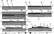
FIGS. 1A-1G illustrate a process for making an IR sensor having a single 2D material based sensor in accordance with one embodiment of the present invention. -
FIGS. 2A-2G illustrate a process for making an IR sensor having a double 2D material based sensor in accordance with another embodiment of the present invention. -
FIG. 3 illustrates a top view of a thermopile IR sensor in accordance with one embodiment of the present invention. -
FIG. 4 illustrates the sensor temperature profile of theFIG. 3 thermopile IR sensor after IR absorption. -
FIG. 5 illustrates a top view of a thermopile array in accordance with one embodiment of the present invention, in which four of theFIG. 3 thermopile IR sensors are provided. - According to the present invention, a thermopile IR sensor and a fabrication method is provided which makes it possible to eliminate the need for a suspended membrane structure ("released" membrane) while still providing enhanced sensitivity. Such thermopile IR sensors are more durable, and are also less complex, costly, and time consuming to fabricate. The thermopile IR sensors of the invention have even been shown to outperform current TP sensor designs based on polycrystalline silicon ("poly-Si").
- The present invention achieves such properties by the use of new thermally isolating materials in combination with ultra-thin materials. In particular, according to embodiments of the invention, a thermopile IR sensor is formed by disposing these new thermally isolating materials between an ultra-thin material based sensor and the substrate.
- According to the present invention, the "new thermally isolating materials" (which may also be referred to herein as simply "thermally isolating materials" or "thermal isolation materials") are polymeric materials that possess very low thermal conductivity as compared to conventional materials, particularly thermal conductivities of less than about 1 W/mK, and are further stable at heightened temperatures, particularly temperatures up to about 450 °C (i.e., heightened temperatures that are lower than 450 °C). Examples of such thermally isolating materials include, but are not limited to Parylene (which includes all forms of Parylene, such as Parylene HT, Parylene N, Parylene C, etc., and can collectively be referred to as "Parylene"), benzocyclobutene (BCB), Cytop™ (amorphous fluoropolymers which can encompasses primary (RPH2), secondary (R2PH), and tertiary (R3P) alkylphosphines where R is linear, branched, cyclic, or which can also contain functional groups), poly(methyl methacrylate), and SU-8 photo-resists.
- For example, the thermal conductivity of Parylene C is 0.084 W/mK, the thermal conductivity of Parylene HT is 0.096 W/mK, and the thermal conductivity of Parylene N is 0.126 W/mK. These values are almost seventeen times lower, almost fifteen times lower and over eleven times lower than SiO2 (1.4 W/mK), respectively. As such, the use of Parylene and other similar thermally isolating materials of the present invention allows for enhanced concentration of heat within the sensor rather than dissipation from the sensor. Further, newly developed forms of Parylene, particularly Parylene HT, are stable at heightened temperatures up to 450°C. This makes the use of Parylene compatible with standard processes in which such heightened temperatures are commonly used. This is in contrast with many conventional materials, which become unstable at heightened temperatures, thus making them unusable with standard processes, such as CMOS processes.
- As referred to herein, the "ultra-thin materials" include any materials having a thickness of less than or equal to 200nm, preferably less than or equal to 100nm. According to embodiments of the present invention, the ultra-thin materials are further characterized in that they are fabricated and deposited at temperatures in excess of 450°C. According to some embodiments, the ultra-thin materials are 2-dimensional (2D) materials. As referred to herein, "2D materials" are generally understood to include materials that have an extremely small thickness in relation to their overall size. More particularly, 2D materials are understood to refer to materials having a thickness of a few nanometers or less, including atomically thin materials which have a thickness of a single atom or a few atoms. Some examples of 2D materials include, but are not limited to, graphene, MoS2, tin selenide (SnSe), black phosphorus (BP), thin poly-silicon (≤ 200nm), SiGe (silicon germanium), Ge (germanium), boron nitride (BN), group III-V compound semiconductors (e.g., boron nitride (BN), boron phosphide (BP), boron arsenide (BAs), aluminum nitride (A1N), aluminum phosphide (A1P), aluminum arsenide (AlAs), aluminum antimonide (AlSb), gallium nitride (GaN), gallium phosphide (GaP), gallium arsenide (GaAs), gallium antimonide (GaSb), indium nitride (InN), indium phosphide (InP), indium arsenide (InAs), Indium antimonide (InSb)), and group II-VI compound semiconductors (e.g., cadmium selenide (CdSe), cadmium sulfide (CdS), cadmium telluride (CdTe), zinc oxide (ZnO), zinc selenide (ZnSe), zinc sulfide (ZnS), and zinc telluride (ZnTe)). The use of such materials beneficially increases the detectivity of the IR sensor.
- Recently, exceptional Seebeck coefficients have been reported for 2D materials. In addition, 2D materials provide outstanding thermoelectric properties (e.g., as high as 105 uVK-1 for MoS2). As such, it is possible to generate more thermoelectric power using 2D materials than with conventional materials, such as poly-silicon which provides thermoelectric properties of about 102 uVK-1. Further, by using 2D material based sensors according to embodiments of the present invention, vacuum packaging and complex doping steps can be omitted, thus making the manufacturing process much simpler.
- However, while the use of ultra-thin and 2D material based sensors provides numerous advantages, such materials still result in rapid dissipation of the absorbed IR light heat into the substrate, thereby not allowing the sensor to heat up sufficiently. Thus, a structure in which 2D materials are used in a thermopile IR sensor still requires the use of a suspended ("released") membrane in order to minimize dissipation and increase sensitivity of the sensor.
- According to the present invention, in addition to using ultra-thin materials, such as 2D materials, the new thermally isolating materials are provided. In particular, the new thermally isolating materials are disposed between the ultra-thin material based sensor and the substrate, thereby creating thermal isolation of the ultra-thin material based sensor to the substrate. By combining the thermally isolating materials, which possess very low thermal conductivity, with the ultra-thin materials, which provide exceptional Seebeck coefficients and outstanding thermoelectric properties, it is possible to provide a thermopile IR sensor in which membrane suspension ("release") is not required in order to prevent fast dissipation of heat into the substrate. As such, the sensor of the present invention is allowed to heat up sufficiently to thereby provide excellent sensitivity.
- The formation of a thermopile IR sensor that combines both ultra-thin materials and the new thermally isolating materials, such as a combination of 2D materials and Parylene, is extremely difficult and has not been achieved to date. Most ultra-thin materials, such as 2D materials, are grown using chemical vapor deposition (CVD). CVD is a process that must be carried out at temperatures as high as 700°C. This heightened temperature is a serious restriction, due to the temperatures at which Parylene becomes unstable. Further, CMOS wafers, printed circuit boards (PCB) and most flexible substrates on which the ultra-thin and 2D materials must be grown in order to form the sensor are likewise limited in their allowable temperature exposure. In particular, such materials generally remain stable up to a maximal temperature exposure of 450°C. As a result, growth of ultra-thin and 2D materials onto such materials is not possible.
- The present invention overcomes these obstacles by providing a wafer transfer technique that allows for the formation of a structure including both ultra-thin materials with heightened temperature restrictions and the new thermally isolating materials. Further, the present techniques make it possible to provide the ultra-thin materials and thermally isolating materials on any desired substrate material, including CMOS wafers, PCBs, flexible substrates, conventional substrate materials, and materials that have heightened temperature limitations.
- In general, the present method deposits the new thermally isolating materials on a desired substrate material (also referred to herein as a substrate wafer), and separately deposits the ultra-thin material on a carrier substrate (also referred to herein as a carrier wafer). As such, the ultra-thin material can be deposited under the necessary heightened temperatures without exposing the new thermally isolating materials, or the substrate on which the new thermally isolating materials are deposited, to such heightened temperatures. Subsequently, the carrier wafer on which the ultra-thin material has been deposited is bonded to the substrate wafer on which the new thermally isolating material has been deposited. According to various embodiments, this bond is formed using Parylene. However, any conventional bonding techniques may be used, including, but not limited to, low temperature direct bonding, fusion, thermo-compression, and various polymer bonding techniques. After bonding, the carrier wafer can be removed using selective etching or any other suitable mechanisms. Thereafter, the sensor material can be structured as needed for the desired end use.
- Referring now to the various figures of the drawing wherein like reference characters refer to like parts, there is shown in
FIGS. 1A-1G , one example of a process for fabricating a thermocouple including a single 2D material layer. In this embodiment, the thermally isolating material is Parylene, the ultra-thin material is a 2D material, and the bonding material is Parylene. However, any other thermally isolating materials, ultra-thin materials, and bonding materials could suitably be used in place of Parylene and a 2D material. - As shown in
FIG. 1A , asubstrate 1 is provided having abottom surface 2 and atop surface 3. Thissubstrate 1 can be fabricated of any conventional substrate materials, including materials that may become unstable at heightened temperatures, such as the heightened temperatures at which ultra-thin materials such as 2D materials are deposited. Some examples of thesubstrate 1 include, but are not limited to, CMOS wafers, printed circuit boards (PCB), polymer substrates, flexible substrates, and silicon/germanium/quartz-wafers. In particular, as shown in the depicted embodiment, inFig. 1A Parylene 4 is deposited on thetop surface 3 of thesubstrate 1. This deposition can be carried out using any conventional method. - As shown in
Fig. 1B , aseparate carrier substrate 5 is provided having a bottom surface 6 and atop surface 7. As depicted, a sacrificial layer 8 may first be provided on thetop surface 7 of thecarrier substrate 5. This sacrificial layer 8 is optional, but it may make subsequent removal of thecarrier substrate 5 easier, and it may further serve as a protective layer, for example, if another etch technique is used to remove the carrier substrate (e.g. DRIE or other wet etch techniques). The2D material 9 is then grown on the sacrificial layer 8 or directly on thecarrier substrate 5top surface 7 if no sacrificial layer 8 is used. In some embodiments, an intermediate layer (not shown) may optionally be provided below the sacrificial layer 8 for better adhesion. In some embodiments, a protective layer (not shown) may optionally be provided on top of the sacrificial layer 8 to protect the 2D material against the sacrificial layer etching step. The sacrificial layer 8 is labeled as a metal, since in an exemplary embodiment the sacrificial layer 8 is copper, which will be etched away using metal wet etching to remove thecarrier substrate 5 of the carrier wafer. In the case of using other etching techniques (e.g. DRIE), the sacrificial layer 8 may be formed as a protective layer, such as SiO2, which acts as an etch stop rather than sacrificial layer. In such embodiments, this layer needs to be removed in a subsequent step to electrically connect the 2D material layer using metal deposition. According to the present invention, thecarrier substrate 5 can be formed of silicon or any other conventional materials that allow for deposition of anultra-thin material 9 thereon either directly or via a sacrificial layer 8 and/or intermediate layer. As such, the material forming thecarrier substrate 5 should be stable at the required conditions at which deposition of these layers is carried out. - Next, as shown in
Fig. 1C , abonding layer 10 is deposited by any conventional deposition methods on top of the2D material layer 9 so as to allow for bonding of the two wafer/substrate assemblies ofFig. 1A and Fig. 1C together. Thisbonding layer 10 can be Parylene, any other thermally isolating material, or any other conventional bonding material, including amorphous and polymer based bonding materials. There are not particular limitations to the selection of the material used as thebonding layer 10, provided that the overall Parylene/bonding layer is thick enough to guarantee thermal isolation. In some embodiments, abonding layer 10 is not provided, and the Parylene 4 layer provided on thesubstrate 1 ofFIG. 1A is utilized as a bonding material. - Next, as shown in
FIG. 1D , the Parylene 4 layer ofFIG. 1A and thebonding layer 10 ofFIG. 1C are placed in contact with each other and the two wafer stacks are bonded together. For example, the carrier wafer assembly inFig. 1C may be flipped upside down and stacked on top of the substrate wafer assembly ofFig. 1A , as shown inFIG. 1D . Of course, any other method can be used so as to provide the two wafer assemblies ofFIG. 1A and 1C in the stacked arrangement and to allow for them to be bonded together (e.g., the substrate wafer assembly ofFIG. 1A can be flipped upside down and stacked on top of the carrier wafer assembly inFIG. 1C , the two wafer assemblies ofFIG. 1A and 1C can be stacked together side by side, etc.). Any variety of bonding techniques can be used, including but not limited to, polymer bonding, low temperature direct bonding, and thermo-compression bonding. As shown in the depicted embodiment, the Parylene 4 layer ofFIG. 1A and thebonding layer 10 ofFIG. 1C are placed in contact with each other and bonded together. Such bonding can be carried out under heightened temperature, application of pressure, and/or possibly O2 plasma treatment. Alternatively, when nobonding layer 10 is provided, the Parylene 4 layer ofFIG. 1A and the2D material 9 layer ofFIG. 1C are placed in contact with each other and bonded together by applying pressure. - After bonding, the
carrier wafer 5 is removed using selective etching or any other conventional process to thereby provide the sensor wafer structure as shown inFIG. 1E . As shown, this structure includes thesubstrate 1, the Parylene 4 layer provided on thetop surface 3 of thesubstrate 1, afurther Parylene 10 layer as a bonding material (if thebonding layer 10 is provided), followed by the2D material 9. For example, in some embodiments, thecarrier wafer 5 may be removed by selectively etching the sacrificial layer 8 using, for example, metal, SiO2 or other selective etching processes. This process removes both the sacrificial layer 8 and the attachedcarrier wafer 5. In some embodiments, prior to the selective etching processes, a wafer grinding process or the like can be performed to remove the bulk of the carrier wafer. Of course, as it would be readily understood by one skilled in the art, any other conventional techniques could alternatively be used to remove thecarrier wafer 5 and the sacrificial layer 8, if provided. - After removal of the sacrificial layer 8 (if included) and the
carrier wafer 5, structuring of the sensor wafer can then be performed. For example, as shown in Fig. IF, Parylene 4, the bonding layer 10 (which is Parylene in this embodiment), and the2D material 9 are structured, with the2D material 9 forming the sensor, to provide a thermal connection to thesubstrate 1. Further, electroplating or metal sputtering is performed to create a thermal stud. In particular, a sputtering process can be carried out so as to connect the thermocouple together and, at the same time, create the thermal contact to thecarrier substrate 1. For a single 2D material sensor, the thermocouple can be formed by the2D material 9 and the sputteredmetal 12. While electroplating may be used, this process requires a seed layer, which might result in short-circuiting the sensor. Thus, metal sputtering is preferred. A cold junction of the sensor can then be achieved by thermally connecting the outer sensor part with thesubstrate 1 through metallization. For example, metal sputtering can be performed to depositmetal 12 which connects the2D material 9 electrically and forms the thermocouple. At the same time, this establishes thermal contact between the2D material 9 and thesubstrate 1, thus forming a cold junction area at the thermopile sensor. - In the resulting structure, the
metal 12 acts as a Seebeck coefficient material. Anabsorber 13 is further deposited as an upper layer so as to absorb IR radiation. Theabsorber 13 can be fabricated of any conventional materials, including but not limited to, interferometric and organic materials, and can further be sized and configured in accordance with conventional absorbers. -
FIGS. 2A-2G depict another embodiment of the present invention in which the fabrication process is similar to the process depicted inFIGS. 1A-1G . The main difference in the embodiment depicted byFIGS. 2A-2G is that a double 2D material layer thermocouple is provided by this embodiment rather than the single 2D material layer thermocouple which is provided byFIGS. 1A-1G . As such, inFIG. 2B , afirst 2D material 29 and asecond 2D material 30 are deposited on thecarrier wafer 25 rather than deposition of thesingle 2D material 9 as shown in FIG. IB. Thefirst 2D material 29 and thesecond 2D material 30 can be, for example, two different 2D or ultrathin materials, wherein "different" 2D or ultrathin materials mean that they possess different Seebeck coefficients. The remainder of the process steps inFIG. 2A-2G may be similar to or essentially the same as those described above in connection withFIGS. 1A-1G . - In particular, in
FIG. 2A ,Parylene 24 is deposited on atop surface 23 of asubstrate wafer 20. InFigure 2B , asacrificial layer 28 may optionally be deposited on atop surface 27 of acarrier wafer 25. Afirst 2D material 29 is subsequently deposited on a portion of the sacrificial layer 28 (or directly onto thecarrier wafer 20 if asacrificial layer 28 is not provided), such as on a left side. Asecond 2D material 30 is, likewise, deposited on another portion of the sacrificial layer (or directly onto thecarrier wafer 20 if asacrificial layer 28 is not provided), such as on a right side. Of course, it will be understood by those skilled in the art that any arrangement of any number of 2D materials (in addition to the structure specifically shown inFIGS. 2A-2G ) could be used and determined based on the desired end structure. A bonding layer 28 (which may be Parylene, a thermally isolating material, or any conventional bonding material), is then optionally deposited on top of the2D materials FIG. 2C . Thereafter, the carrier wafer assembly inFig. 2C is flipped upside down and stacked on top of the substrate wafer assembly formed inFig. 2A (or, as noted above in connection withFIG. 2D , any other method can be used so as to stack the substrate wafer assembly ofFIG. 2A and the carrier wafer assembly ofFIG. 2C together). The carrier wafer assembly and the substrate wafer assembly are then bonded together using any variety of bonding techniques to provide the structure ofFIG. 2D . After bonding, thecarrier wafer 25 is removed using selective etching or any other conventional process to thereby provide the sensor wafer structure as shown inFIG. 2E . As shown, the sensor wafer structure includes thesubstrate 20, theParylene 24 layer provided on thetop surface 23 of thesubstrate 20, afurther Parylene 40 layer as a bonding material, followed by the2D materials - After removal of the sacrificial layer 28 (if included) and the
carrier wafer 25, structuring of the sensor wafer shown inFIG. 2E can then be performed. For example, as shown inFig. 2F ,Parylene 24, thebonding layer 40 and the2D materials 2D materials substrate 1. Further, electroplating is performed to create a thermal stud, and a cold junction of the sensor can then be achieved by thermally connecting the outer sensor part with thesubstrate 20 through metallization. For example, metal sputtering can be performed to depositmetal 32 which connects the2D materials 2D materials substrate 20, thus forming a cold junction area at the thermopile sensor. Anabsorber 33 is further deposited as an upper layer so as to absorb IR radiation. -
FIG. 3 depicts a top view of a thermopile IR sensor according to an embodiment of the present invention which includes a double2D material layer Parylene 40 when used as a bonding material) as a thermally isolating material disposed between the2D material layer substrate 20. The thermopile IR sensor depicted can be fabricated, for example, in accordance with the embodiment shown inFIG. 2A-2G . It is noted that thesubstrate 20 is not depicted in this view because it is positioned directly below the Parylene layers 24, 40. - The temperature profile of the structure shown in
FIG. 3 is further depicted inFIG. 4 . In particular, the figure shows the heat distribution within the sensor upon incoming radiation of IR light. First the IR-light will be converted into heat by the absorber layer. Afterwards the heat spreads over the entire structure. Depicted is a steady state, and as demonstrated, the heat spread has reached saturation after a curtain time. As shown, most of the heat is concentrated at the middle of the sensor, and there is a temperature difference between the middle of the sensor and the edge. This temperature difference, together with the Seebeck coefficient difference of the 2D materials is creating a voltage output. Generally, the larger the temperature difference the better - According to embodiments of the present invention, the thermopile IR sensor can comprise several thermocouples, which are electrically connected in series. An array of thermopile sensors can further be built. For example, a plurality of
thermocouples 100 can be electrically connected to provide athermopile array 102 such as that shown inFIG. 5 . In particular,FIG. 5 depicts an array of four thermopile IR sensors, which may be sensors in accordance with the embodiment shown inFIG. 3 , arranged in two rows. Of course, while thethermopile array 102 is depicted as comprising four thermopile IR sensors arranged in two rows, one or ordinary skill will appreciate that any number of thermopile IR sensors may be included and arranged in any desired configuration. - By using the present wafer/substrate bonding methods, ultra-thin materials can be grown at the requisite temperatures of up to 700°C, while overcoming the thermal instability issues of Parylene and other thermally isolating materials, as well as the allowable temperature budget for fabricating various wafers. The present wafer bonding methods can also be used to directly bond a thermopile sensor on any substrate, including but not limited to, silicon wafers, CMOS wafers, a printed circuit boards (PCB) and other desired flexible substrates, which may even have heightened temperature restrictions. Some examples of flexible substrates include, but are not limited to polyimide, PEEK (Polyether ether ketone) and transparent conductive polyesters. Such methods are beneficial because there is a challenge to integrating a CVD grown material onto a CMOS wafer, PCB or flexible substrate having a maximum allowable temperature of 450°C. The present invention makes it possible to fabricate such structures regardless of temperature restrictions by growing the desired material on a first wafer at the requisite heightened temperature, followed by subsequently bonding the grown material to the CMOS wafer, PCB or flexible substrate. Still further, the present materials and methods allow for the use of a thinner substrate and, thus, for applications where mechanical flexibility of the sensor is required, such structures can now be realized.
- In addition, the present invention provides for the possibility of thermally isolating the sensor using novel materials, such as Parylene, which makes it unnecessary to suspend/release the membrane in order to achieve a high sensitivity. As a result, the overall fabrication process is simplified and the resulting structure is very robust for the subsequent handling and packaging steps. This will lead to cost reductions due to a higher yield of products and a simpler manufacturing process.
- The methods and devices provided by the present invention will find great use in a variety of applications, including all known thermopile array types, especially in small array applications, air conditioning systems, the automotive industry, consumer electronics, presence and motion detection, people counting, and wearable sensors.
- It will be apparent to those skilled in the art that various modifications and variations can be made to the structure of the present invention without departing from the scope of the invention, which is defined by the appended claims.
- In view of the foregoing, it is intended that the present invention cover modifications and variations of this invention provided they fall within the scope of the following claims.
Claims (15)
- An unreleased thermopile infrared sensor comprising:a substrate (1) having a bottom surface and a top surface;a thermally isolating material (4) disposed on at least a portion of the top surface of the substrate, the thermally isolating material having a bottom surface and a top surface; anda 2D material (9, 29) disposed on at least a portion of the top surface of the thermally isolating material, the 2D material having a thickness of a few nanometers or less;wherein the thermally isolating material comprises a polymeric material possessing a thermal conductivity of less than about 1 W/m.K and is stable at temperatures up to 450°C, andwherein the 2D material is configured to be deposited at a temperature greater than 450°C, and, wherein the 2D material is forming one of the two electrical conductors of a thermocouple of the thermopile sensor.
- The unreleased thermopile infrared sensor of claim 1, wherein the thermally isolating material is selected from Parylene,benzocyclobutene (BCB), amorphous fluoropolymers, poly(methyl methacrylate), SU-8 photo-resists, and other polymers.
- The unreleased thermopile infrared sensor of claim 1, wherein the 2D material is one or more materials selected from the group consisting of graphene, MoS2, SnSe, black phosphorus (BP), thin poly-silicon, SiGe (silicon germanium), Ge (germanium), boron nitride (BN), group III-V compound semiconductors, group II-VI compound semiconductors, and combinations thereof.
- The unreleased thermopile infrared sensor of claim 1, further comprising a second 2D material (30) disposed on at least another portion of the top surface of the thermally isolating material, wherein the second 2D material is forming the second electrical conductor of the thermocouple.
- The unreleased thermopile infrared sensor of claim 1, wherein the substrate is selected from a silicon wafer, a CMOS wafer, a printed circuit board, or a flexible substrate that is unstable at temperatures in excess of 450°C.
- The unreleased thermopile infrared sensor of claim 1, wherein the thermally isolating material (4) is Parylene, and the substrate is preferably selected from a silicon wafer, a CMOS wafer, a printed circuit board, or a flexible substrate that is unstable at temperatures in excess of 450°C.
- A method for fabricating an unreleased thermopile infrared sensor comprising:(a) forming a substrate assembly by providing a substrate layer (1) having a bottom surface and a top surface, and depositing a thermally isolating material layer (4) on at least a portion of the top surface of the substrate layer, wherein the thermally isolating material layer comprises a polymeric material possessing a thermal conductivity of less than about 1 W/mk;(b) forming a carrier assembly by providing a carrier layer (25) having a bottom surface and a top surface, optionally depositing a sacrificial layer (28) on at least a portion of the top surface of the carrier layer, depositing an ultra-thin material layer (9, 29, 30) on at least a portion of the sacrificial layer or on at least a portion of the top surface of the carrier layer, and optionally depositing a bonding layer on the ultra-thin material;(c) stacking the carrier assembly on top of the substrate assembly by placing the ultra-thin material layer or bonding layer of the carrier assembly into contact with the thermally isolating material layer of the substrate assembly;(d) bonding the carrier assembly to the substrate assembly to provide a bonded stack;(e) removing the carrier layer and optional sacrificial layer from the bonded stack to provide a sensor wafer, the sensor wafer comprising the substrate layer, the thermally isolating material layer on the top surface of the substrate layer, the optional bonding layer on the thermally isolating material layer, and the ultra-thin material layer on the optional bonding layer or on the thermally isolating material layer; and(f) structuring the sensor wafer to provide the unreleased thermopile infrared sensor,
wherein the thermally isolating material layer is stable at temperatures up to 450°C, and the ultra-thin material layer is fabricated of one or more materials having a thickness of less than or equal to 200 nm and is deposited by methods requiring a heightened temperature of greater than 450°C. - The method of claim 7, wherein the substrate layer comprises one or more materials that are unstable at temperatures greater than 450°C, a CMOS wafer, a printed circuit board (PCB), or a flexible substrate that is unstable at temperatures greater than 450°C.
- The method of claim 7, wherein the carrier substrate is fabricated of silicon, or any other material that is stable under conditions at which the ultra-thin material layer is deposited.
- The method of claim 7, wherein the thermally isolating material layer is fabricated of one or more materials selected from the group consisting of Parylene, benzocyclobutene (BCB), amorphous fluoropolymers, poly(methyl methacrylate), SU-8 photo-resists, and other polymers.
- The method of claim 7, wherein the ultra-thin material layer is fabricated of one or more 2D materials, preferably one or more materials selected from the group consisting of graphene, MoS2, SnSe, black phosphorus (BP), thin poly-silicon, SiGe (silicon germanium), Ge (germanium), boron nitride (BN), group III-V compound semiconductors, and group II-VI compound semiconductors.
- The method of claim 7, wherein the optional bonding layer is fabricated of one or more polymeric materials that are stable at temperatures up to 450°C.
- The method of claim 7, wherein the step of bonding the carrier assembly to the substrate assembly is carried out using polymer bonding, low temperature direct bonding, fusion bonding, and/or thermo-compression bonding.
- The method of claim 7, wherein the carrier layer and sacrificial layer are removed from the bonded stack by selective etching of the sacrificial layer, and preferably wherein prior to selective etching, a wafer grinding process is performed to remove a bulk of the carrier wafer.
- A method as claimed in claim 7, wherein the thermally isolating material (4) is Parylene, and the ultra-thin material is a 2D material.
Applications Claiming Priority (1)
| Application Number | Priority Date | Filing Date | Title |
|---|---|---|---|
| US15/194,753 US9915567B2 (en) | 2016-06-28 | 2016-06-28 | Unreleased thermopile infrared sensor using material transfer method |
Publications (2)
| Publication Number | Publication Date |
|---|---|
| EP3270129A1 EP3270129A1 (en) | 2018-01-17 |
| EP3270129B1 true EP3270129B1 (en) | 2021-01-06 |
Family
ID=59215609
Family Applications (1)
| Application Number | Title | Priority Date | Filing Date |
|---|---|---|---|
| EP17177692.5A Active EP3270129B1 (en) | 2016-06-28 | 2017-06-23 | Unreleased thermopile infrared sensor using material transfer method |
Country Status (4)
| Country | Link |
|---|---|
| US (1) | US9915567B2 (en) |
| EP (1) | EP3270129B1 (en) |
| JP (1) | JP6982414B2 (en) |
| CN (1) | CN107543619B (en) |
Families Citing this family (7)
| Publication number | Priority date | Publication date | Assignee | Title |
|---|---|---|---|---|
| US10326044B2 (en) | 2017-08-18 | 2019-06-18 | Micron Technology, Inc. | Method and apparatus for processing semiconductor device structures |
| CN108550640B (en) * | 2018-04-17 | 2020-02-28 | 张晗 | Broadband black phosphorus photodetector composited with cadmium telluride nanocrystals and preparation method thereof |
| WO2020086004A1 (en) * | 2018-10-26 | 2020-04-30 | National University Of Singapore | Thermocouple, thermopile and devices |
| DE102019211468A1 (en) | 2019-07-31 | 2021-02-04 | Fraunhofer-Gesellschaft zur Förderung der angewandten Forschung e.V. | VERTICAL CONNECTING SEMI-CONDUCTOR STRUCTURE AND METHOD OF MAKING THE SAME |
| CN112113669B (en) * | 2020-08-28 | 2021-08-13 | 哈尔滨工业大学 | A kind of fish-scale hollow SnSe nanotube self-powered infrared detector and preparation method thereof |
| WO2024048473A1 (en) * | 2022-08-31 | 2024-03-07 | パナソニックIpマネジメント株式会社 | Thermoelectric conversion element and method for manufacturing thermoelectric conversion element |
| US12540855B2 (en) * | 2023-08-07 | 2026-02-03 | City University Of Hong Kong | Wide-band photodetectors using thermoelectric materials |
Family Cites Families (24)
| Publication number | Priority date | Publication date | Assignee | Title |
|---|---|---|---|---|
| US4935345A (en) * | 1987-04-07 | 1990-06-19 | Arizona Board Of Regents | Implantable microelectronic biochemical sensor incorporating thin film thermopile |
| EP0867701A1 (en) * | 1997-03-28 | 1998-09-30 | Interuniversitair Microelektronica Centrum Vzw | Method of fabrication of an infrared radiation detector and more particularly an infrared sensitive bolometer |
| SE0000148D0 (en) * | 2000-01-17 | 2000-01-17 | Forskarpatent I Syd Ab | Manufacturing method for IR detector matrices |
| WO2004023087A1 (en) * | 2002-09-09 | 2004-03-18 | Rosemount Aerospace, Inc. | Method for making an infrared detector and infrared detector |
| CN100562725C (en) * | 2003-09-29 | 2009-11-25 | 中国科学院上海微系统与信息技术研究所 | Micromechanical thermopile infrared detector and manufacturing method thereof |
| JP2006071601A (en) | 2004-09-06 | 2006-03-16 | Denso Corp | Infrared sensor, infrared gas detector, and infrared light source |
| CN101071842A (en) * | 2006-05-09 | 2007-11-14 | 中国科学院电子学研究所 | Self-test micromechanical thermoelectric pile bioreaction heat detector and its preparing method |
| US8071487B2 (en) * | 2006-08-15 | 2011-12-06 | United Microelectronics Corp. | Patterning method using stacked structure |
| CN101575083B (en) * | 2009-06-15 | 2011-11-09 | 中北大学 | Micromachined thermopile infrared detector |
| US8587083B2 (en) | 2009-06-17 | 2013-11-19 | Gunnar Malm | Microbolometer semiconductor material |
| DE102010031829B4 (en) | 2009-07-21 | 2021-11-11 | Novaled Gmbh | Thermoelectric components with thin layers |
| JP2013524541A (en) * | 2010-04-14 | 2013-06-17 | エクセリタス カナダ,インコーポレイテッド | Laminated thermopile |
| WO2011136203A1 (en) * | 2010-04-26 | 2011-11-03 | 株式会社エッチ.エム.イー. | Temperature sensor device and radiation thermometer using same, method for producing temperature sensor device, multilayered thin film thermopile using photoresist film and radiation thermometer using same, and method for producing multilayered thin film thermopile |
| CN102918369A (en) * | 2010-05-20 | 2013-02-06 | 日本电气株式会社 | Bolometer and method for manufacturing the same |
| WO2012082801A2 (en) | 2010-12-13 | 2012-06-21 | The Board Of Regents For Oklahoma State University | Nanowire thermoelectric infrared detector |
| DE102011103818A1 (en) * | 2011-06-01 | 2012-12-06 | Meas Deutschland Gmbh | Infrared sensor arrangement and its use |
| US8758650B2 (en) * | 2011-07-05 | 2014-06-24 | Excelitas Technologies Singapore Pte. Ltd. | Graphene-based thermopile |
| CN102798474B (en) * | 2012-08-23 | 2014-02-19 | 江苏物联网研究发展中心 | A high-performance MEMS thermopile infrared detector structure and its preparation method |
| KR101910575B1 (en) * | 2013-01-10 | 2018-10-22 | 삼성전자주식회사 | Infrared detector and infrared image sensor |
| KR102093441B1 (en) * | 2013-03-11 | 2020-03-25 | 삼성전자주식회사 | A method for preparing grapheme |
| US20160097681A1 (en) * | 2013-03-14 | 2016-04-07 | Qualcomm Mems Technologies, Inc. | Microbolometer supported by glass substrate |
| ITTO20130502A1 (en) * | 2013-06-18 | 2014-12-19 | St Microelectronics Asia | ELECTRONIC DEVICE WITH INTEGRATED TEMPERATURE SENSOR AND ITS MANUFACTURING METHOD |
| US20160079306A1 (en) * | 2014-09-12 | 2016-03-17 | Excelitas Technologies Singapore Pte. Ltd. | Surface Micro-Machined Infrared Sensor Using Highly Temperature Stable Interferometric Absorber |
| US9917242B2 (en) * | 2015-03-27 | 2018-03-13 | Maxim Integrated Products, Inc. | Thermopile temperature sensor field of view narrowing using integrated light blocking layer and lens |
-
2016
- 2016-06-28 US US15/194,753 patent/US9915567B2/en active Active
-
2017
- 2017-06-21 JP JP2017121290A patent/JP6982414B2/en active Active
- 2017-06-23 EP EP17177692.5A patent/EP3270129B1/en active Active
- 2017-06-27 CN CN201710501183.9A patent/CN107543619B/en active Active
Non-Patent Citations (1)
| Title |
|---|
| None * |
Also Published As
| Publication number | Publication date |
|---|---|
| JP6982414B2 (en) | 2021-12-17 |
| US9915567B2 (en) | 2018-03-13 |
| CN107543619A (en) | 2018-01-05 |
| EP3270129A1 (en) | 2018-01-17 |
| JP2018013473A (en) | 2018-01-25 |
| US20170370779A1 (en) | 2017-12-28 |
| CN107543619B (en) | 2020-09-29 |
Similar Documents
| Publication | Publication Date | Title |
|---|---|---|
| US9915567B2 (en) | Unreleased thermopile infrared sensor using material transfer method | |
| US9472588B1 (en) | Monolithic visible-infrared focal plane array on silicon | |
| EP1443568B1 (en) | Micro-fabricated device with thermoelectric device and method of making | |
| EP2995916B1 (en) | Surface micro-machined infrared sensor using highly temperature stable interferometric absorber | |
| US11381761B2 (en) | Phononically-enhanced imager (PEI) pixel | |
| WO2014105233A2 (en) | Processes for multi-layer devices utilizing layer transfer | |
| US7785002B2 (en) | P-N junction based thermal detector | |
| US7777229B2 (en) | Method and apparatus for reducing smear in back-illuminated imaging sensors | |
| US20150340542A1 (en) | Pixelated silicon cells or integrated circuits | |
| US12484444B2 (en) | Integrated thermal sensor and manufacturing process thereof | |
| US20170358702A1 (en) | Substrate-free thin-film flexible photovoltaic device and fabrication method | |
| EP3533085B1 (en) | Integrated thermoelectric generator and related method of fabrication | |
| US10096736B1 (en) | P-Type chalcogenide and n-type silicon heterojunction infared photodiodes and method of manufacturing thereof | |
| US9929333B1 (en) | IR thermopile sensor with temperature reference formed in front-end process | |
| KR101072290B1 (en) | thermoelectric sensor using Ge material | |
| JP7448957B2 (en) | Integrated circuit device and its manufacturing method | |
| US20240276882A1 (en) | Multistage Thermoelectric Cooler with Phononic Structure | |
| EP4339568A1 (en) | Infrared sensor, and method for manufacturing infrared sensor | |
| US20220028907A1 (en) | Composite substrate for fabricating iii-v photodetector arrays | |
| US20160322419A1 (en) | Photodetector and methods of manufacture | |
| KR100704378B1 (en) | Semiconductor device and manufacturing method thereof | |
| JP3235361B2 (en) | Infrared detector | |
| CN121692984A (en) | Infrared thermopile sensor and preparation method thereof |
Legal Events
| Date | Code | Title | Description |
|---|---|---|---|
| PUAI | Public reference made under article 153(3) epc to a published international application that has entered the european phase |
Free format text: ORIGINAL CODE: 0009012 |
|
| STAA | Information on the status of an ep patent application or granted ep patent |
Free format text: STATUS: THE APPLICATION HAS BEEN PUBLISHED |
|
| AK | Designated contracting states |
Kind code of ref document: A1 Designated state(s): AL AT BE BG CH CY CZ DE DK EE ES FI FR GB GR HR HU IE IS IT LI LT LU LV MC MK MT NL NO PL PT RO RS SE SI SK SM TR |
|
| AX | Request for extension of the european patent |
Extension state: BA ME |
|
| STAA | Information on the status of an ep patent application or granted ep patent |
Free format text: STATUS: REQUEST FOR EXAMINATION WAS MADE |
|
| 17P | Request for examination filed |
Effective date: 20180716 |
|
| RBV | Designated contracting states (corrected) |
Designated state(s): AL AT BE BG CH CY CZ DE DK EE ES FI FR GB GR HR HU IE IS IT LI LT LU LV MC MK MT NL NO PL PT RO RS SE SI SK SM TR |
|
| STAA | Information on the status of an ep patent application or granted ep patent |
Free format text: STATUS: EXAMINATION IS IN PROGRESS |
|
| 17Q | First examination report despatched |
Effective date: 20191104 |
|
| GRAP | Despatch of communication of intention to grant a patent |
Free format text: ORIGINAL CODE: EPIDOSNIGR1 |
|
| STAA | Information on the status of an ep patent application or granted ep patent |
Free format text: STATUS: GRANT OF PATENT IS INTENDED |
|
| INTG | Intention to grant announced |
Effective date: 20200812 |
|
| GRAS | Grant fee paid |
Free format text: ORIGINAL CODE: EPIDOSNIGR3 |
|
| GRAA | (expected) grant |
Free format text: ORIGINAL CODE: 0009210 |
|
| STAA | Information on the status of an ep patent application or granted ep patent |
Free format text: STATUS: THE PATENT HAS BEEN GRANTED |
|
| AK | Designated contracting states |
Kind code of ref document: B1 Designated state(s): AL AT BE BG CH CY CZ DE DK EE ES FI FR GB GR HR HU IE IS IT LI LT LU LV MC MK MT NL NO PL PT RO RS SE SI SK SM TR |
|
| REG | Reference to a national code |
Ref country code: GB Ref legal event code: FG4D |
|
| REG | Reference to a national code |
Ref country code: AT Ref legal event code: REF Ref document number: 1352874 Country of ref document: AT Kind code of ref document: T Effective date: 20210115 Ref country code: CH Ref legal event code: EP |
|
| REG | Reference to a national code |
Ref country code: DE Ref legal event code: R096 Ref document number: 602017030790 Country of ref document: DE |
|
| REG | Reference to a national code |
Ref country code: IE Ref legal event code: FG4D |
|
| REG | Reference to a national code |
Ref country code: NL Ref legal event code: MP Effective date: 20210106 |
|
| REG | Reference to a national code |
Ref country code: AT Ref legal event code: MK05 Ref document number: 1352874 Country of ref document: AT Kind code of ref document: T Effective date: 20210106 |
|
| REG | Reference to a national code |
Ref country code: LT Ref legal event code: MG9D |
|
| PG25 | Lapsed in a contracting state [announced via postgrant information from national office to epo] |
Ref country code: BG Free format text: LAPSE BECAUSE OF FAILURE TO SUBMIT A TRANSLATION OF THE DESCRIPTION OR TO PAY THE FEE WITHIN THE PRESCRIBED TIME-LIMIT Effective date: 20210406 Ref country code: LT Free format text: LAPSE BECAUSE OF FAILURE TO SUBMIT A TRANSLATION OF THE DESCRIPTION OR TO PAY THE FEE WITHIN THE PRESCRIBED TIME-LIMIT Effective date: 20210106 Ref country code: GR Free format text: LAPSE BECAUSE OF FAILURE TO SUBMIT A TRANSLATION OF THE DESCRIPTION OR TO PAY THE FEE WITHIN THE PRESCRIBED TIME-LIMIT Effective date: 20210407 Ref country code: FI Free format text: LAPSE BECAUSE OF FAILURE TO SUBMIT A TRANSLATION OF THE DESCRIPTION OR TO PAY THE FEE WITHIN THE PRESCRIBED TIME-LIMIT Effective date: 20210106 Ref country code: HR Free format text: LAPSE BECAUSE OF FAILURE TO SUBMIT A TRANSLATION OF THE DESCRIPTION OR TO PAY THE FEE WITHIN THE PRESCRIBED TIME-LIMIT Effective date: 20210106 Ref country code: PT Free format text: LAPSE BECAUSE OF FAILURE TO SUBMIT A TRANSLATION OF THE DESCRIPTION OR TO PAY THE FEE WITHIN THE PRESCRIBED TIME-LIMIT Effective date: 20210506 Ref country code: NO Free format text: LAPSE BECAUSE OF FAILURE TO SUBMIT A TRANSLATION OF THE DESCRIPTION OR TO PAY THE FEE WITHIN THE PRESCRIBED TIME-LIMIT Effective date: 20210406 |
|
| PG25 | Lapsed in a contracting state [announced via postgrant information from national office to epo] |
Ref country code: SE Free format text: LAPSE BECAUSE OF FAILURE TO SUBMIT A TRANSLATION OF THE DESCRIPTION OR TO PAY THE FEE WITHIN THE PRESCRIBED TIME-LIMIT Effective date: 20210106 Ref country code: AT Free format text: LAPSE BECAUSE OF FAILURE TO SUBMIT A TRANSLATION OF THE DESCRIPTION OR TO PAY THE FEE WITHIN THE PRESCRIBED TIME-LIMIT Effective date: 20210106 Ref country code: RS Free format text: LAPSE BECAUSE OF FAILURE TO SUBMIT A TRANSLATION OF THE DESCRIPTION OR TO PAY THE FEE WITHIN THE PRESCRIBED TIME-LIMIT Effective date: 20210106 Ref country code: PL Free format text: LAPSE BECAUSE OF FAILURE TO SUBMIT A TRANSLATION OF THE DESCRIPTION OR TO PAY THE FEE WITHIN THE PRESCRIBED TIME-LIMIT Effective date: 20210106 Ref country code: LV Free format text: LAPSE BECAUSE OF FAILURE TO SUBMIT A TRANSLATION OF THE DESCRIPTION OR TO PAY THE FEE WITHIN THE PRESCRIBED TIME-LIMIT Effective date: 20210106 |
|
| PG25 | Lapsed in a contracting state [announced via postgrant information from national office to epo] |
Ref country code: IS Free format text: LAPSE BECAUSE OF FAILURE TO SUBMIT A TRANSLATION OF THE DESCRIPTION OR TO PAY THE FEE WITHIN THE PRESCRIBED TIME-LIMIT Effective date: 20210506 |
|
| REG | Reference to a national code |
Ref country code: DE Ref legal event code: R097 Ref document number: 602017030790 Country of ref document: DE |
|
| PG25 | Lapsed in a contracting state [announced via postgrant information from national office to epo] |
Ref country code: CZ Free format text: LAPSE BECAUSE OF FAILURE TO SUBMIT A TRANSLATION OF THE DESCRIPTION OR TO PAY THE FEE WITHIN THE PRESCRIBED TIME-LIMIT Effective date: 20210106 Ref country code: EE Free format text: LAPSE BECAUSE OF FAILURE TO SUBMIT A TRANSLATION OF THE DESCRIPTION OR TO PAY THE FEE WITHIN THE PRESCRIBED TIME-LIMIT Effective date: 20210106 Ref country code: SM Free format text: LAPSE BECAUSE OF FAILURE TO SUBMIT A TRANSLATION OF THE DESCRIPTION OR TO PAY THE FEE WITHIN THE PRESCRIBED TIME-LIMIT Effective date: 20210106 |
|
| PLBE | No opposition filed within time limit |
Free format text: ORIGINAL CODE: 0009261 |
|
| STAA | Information on the status of an ep patent application or granted ep patent |
Free format text: STATUS: NO OPPOSITION FILED WITHIN TIME LIMIT |
|
| PG25 | Lapsed in a contracting state [announced via postgrant information from national office to epo] |
Ref country code: RO Free format text: LAPSE BECAUSE OF FAILURE TO SUBMIT A TRANSLATION OF THE DESCRIPTION OR TO PAY THE FEE WITHIN THE PRESCRIBED TIME-LIMIT Effective date: 20210106 Ref country code: SK Free format text: LAPSE BECAUSE OF FAILURE TO SUBMIT A TRANSLATION OF THE DESCRIPTION OR TO PAY THE FEE WITHIN THE PRESCRIBED TIME-LIMIT Effective date: 20210106 Ref country code: DK Free format text: LAPSE BECAUSE OF FAILURE TO SUBMIT A TRANSLATION OF THE DESCRIPTION OR TO PAY THE FEE WITHIN THE PRESCRIBED TIME-LIMIT Effective date: 20210106 |
|
| 26N | No opposition filed |
Effective date: 20211007 |
|
| PG25 | Lapsed in a contracting state [announced via postgrant information from national office to epo] |
Ref country code: AL Free format text: LAPSE BECAUSE OF FAILURE TO SUBMIT A TRANSLATION OF THE DESCRIPTION OR TO PAY THE FEE WITHIN THE PRESCRIBED TIME-LIMIT Effective date: 20210106 Ref country code: MC Free format text: LAPSE BECAUSE OF FAILURE TO SUBMIT A TRANSLATION OF THE DESCRIPTION OR TO PAY THE FEE WITHIN THE PRESCRIBED TIME-LIMIT Effective date: 20210106 Ref country code: ES Free format text: LAPSE BECAUSE OF FAILURE TO SUBMIT A TRANSLATION OF THE DESCRIPTION OR TO PAY THE FEE WITHIN THE PRESCRIBED TIME-LIMIT Effective date: 20210106 |
|
| REG | Reference to a national code |
Ref country code: CH Ref legal event code: PL |
|
| PG25 | Lapsed in a contracting state [announced via postgrant information from national office to epo] |
Ref country code: SI Free format text: LAPSE BECAUSE OF FAILURE TO SUBMIT A TRANSLATION OF THE DESCRIPTION OR TO PAY THE FEE WITHIN THE PRESCRIBED TIME-LIMIT Effective date: 20210106 |
|
| REG | Reference to a national code |
Ref country code: BE Ref legal event code: MM Effective date: 20210630 |
|
| PG25 | Lapsed in a contracting state [announced via postgrant information from national office to epo] |
Ref country code: LU Free format text: LAPSE BECAUSE OF NON-PAYMENT OF DUE FEES Effective date: 20210623 |
|
| PG25 | Lapsed in a contracting state [announced via postgrant information from national office to epo] |
Ref country code: LI Free format text: LAPSE BECAUSE OF NON-PAYMENT OF DUE FEES Effective date: 20210630 Ref country code: IT Free format text: LAPSE BECAUSE OF FAILURE TO SUBMIT A TRANSLATION OF THE DESCRIPTION OR TO PAY THE FEE WITHIN THE PRESCRIBED TIME-LIMIT Effective date: 20210106 Ref country code: IE Free format text: LAPSE BECAUSE OF NON-PAYMENT OF DUE FEES Effective date: 20210623 Ref country code: CH Free format text: LAPSE BECAUSE OF NON-PAYMENT OF DUE FEES Effective date: 20210630 |
|
| PG25 | Lapsed in a contracting state [announced via postgrant information from national office to epo] |
Ref country code: IS Free format text: LAPSE BECAUSE OF FAILURE TO SUBMIT A TRANSLATION OF THE DESCRIPTION OR TO PAY THE FEE WITHIN THE PRESCRIBED TIME-LIMIT Effective date: 20210506 |
|
| PG25 | Lapsed in a contracting state [announced via postgrant information from national office to epo] |
Ref country code: BE Free format text: LAPSE BECAUSE OF NON-PAYMENT OF DUE FEES Effective date: 20210630 |
|
| PG25 | Lapsed in a contracting state [announced via postgrant information from national office to epo] |
Ref country code: HU Free format text: LAPSE BECAUSE OF FAILURE TO SUBMIT A TRANSLATION OF THE DESCRIPTION OR TO PAY THE FEE WITHIN THE PRESCRIBED TIME-LIMIT; INVALID AB INITIO Effective date: 20170623 |
|
| P01 | Opt-out of the competence of the unified patent court (upc) registered |
Effective date: 20230524 |
|
| PG25 | Lapsed in a contracting state [announced via postgrant information from national office to epo] |
Ref country code: NL Free format text: LAPSE BECAUSE OF NON-PAYMENT OF DUE FEES Effective date: 20210206 Ref country code: CY Free format text: LAPSE BECAUSE OF FAILURE TO SUBMIT A TRANSLATION OF THE DESCRIPTION OR TO PAY THE FEE WITHIN THE PRESCRIBED TIME-LIMIT Effective date: 20210106 |
|
| PG25 | Lapsed in a contracting state [announced via postgrant information from national office to epo] |
Ref country code: MK Free format text: LAPSE BECAUSE OF FAILURE TO SUBMIT A TRANSLATION OF THE DESCRIPTION OR TO PAY THE FEE WITHIN THE PRESCRIBED TIME-LIMIT Effective date: 20210106 |
|
| PG25 | Lapsed in a contracting state [announced via postgrant information from national office to epo] |
Ref country code: TR Free format text: LAPSE BECAUSE OF FAILURE TO SUBMIT A TRANSLATION OF THE DESCRIPTION OR TO PAY THE FEE WITHIN THE PRESCRIBED TIME-LIMIT Effective date: 20210106 |
|
| PG25 | Lapsed in a contracting state [announced via postgrant information from national office to epo] |
Ref country code: MT Free format text: LAPSE BECAUSE OF FAILURE TO SUBMIT A TRANSLATION OF THE DESCRIPTION OR TO PAY THE FEE WITHIN THE PRESCRIBED TIME-LIMIT Effective date: 20210106 |
|
| PGFP | Annual fee paid to national office [announced via postgrant information from national office to epo] |
Ref country code: GB Payment date: 20260629 Year of fee payment: 10 |
|
| PGFP | Annual fee paid to national office [announced via postgrant information from national office to epo] |
Ref country code: DE Payment date: 20260629 Year of fee payment: 10 |
|
| PGFP | Annual fee paid to national office [announced via postgrant information from national office to epo] |
Ref country code: FR Payment date: 20260625 Year of fee payment: 10 |