EP3270053A1 - A housing for lighting devices, corresponding lighting device and method - Google Patents
A housing for lighting devices, corresponding lighting device and method Download PDFInfo
- Publication number
- EP3270053A1 EP3270053A1 EP17180022.0A EP17180022A EP3270053A1 EP 3270053 A1 EP3270053 A1 EP 3270053A1 EP 17180022 A EP17180022 A EP 17180022A EP 3270053 A1 EP3270053 A1 EP 3270053A1
- Authority
- EP
- European Patent Office
- Prior art keywords
- electrically conductive
- housing
- conductive lines
- channel
- light radiation
- Prior art date
- Legal status (The legal status is an assumption and is not a legal conclusion. Google has not performed a legal analysis and makes no representation as to the accuracy of the status listed.)
- Granted
Links
- 238000000034 method Methods 0.000 title claims description 9
- 230000005855 radiation Effects 0.000 claims abstract description 47
- 230000015572 biosynthetic process Effects 0.000 claims abstract description 9
- 238000005755 formation reaction Methods 0.000 claims abstract description 9
- 238000007789 sealing Methods 0.000 claims description 5
- 239000007787 solid Substances 0.000 claims description 4
- 239000000463 material Substances 0.000 description 14
- 239000000243 solution Substances 0.000 description 12
- 230000001681 protective effect Effects 0.000 description 7
- 239000004020 conductor Substances 0.000 description 5
- 238000004519 manufacturing process Methods 0.000 description 5
- 239000011295 pitch Substances 0.000 description 4
- 238000004382 potting Methods 0.000 description 4
- 239000003795 chemical substances by application Substances 0.000 description 3
- 238000002347 injection Methods 0.000 description 3
- 239000007924 injection Substances 0.000 description 3
- 239000011810 insulating material Substances 0.000 description 3
- 239000010410 layer Substances 0.000 description 3
- RYGMFSIKBFXOCR-UHFFFAOYSA-N Copper Chemical compound [Cu] RYGMFSIKBFXOCR-UHFFFAOYSA-N 0.000 description 2
- 239000000853 adhesive Substances 0.000 description 2
- 230000001070 adhesive effect Effects 0.000 description 2
- 230000005540 biological transmission Effects 0.000 description 2
- 229910052802 copper Inorganic materials 0.000 description 2
- 239000010949 copper Substances 0.000 description 2
- 238000010292 electrical insulation Methods 0.000 description 2
- 238000003780 insertion Methods 0.000 description 2
- 230000037431 insertion Effects 0.000 description 2
- 238000009434 installation Methods 0.000 description 2
- 239000002184 metal Substances 0.000 description 2
- 229910052751 metal Inorganic materials 0.000 description 2
- 230000035515 penetration Effects 0.000 description 2
- 229920000642 polymer Polymers 0.000 description 2
- 229920001296 polysiloxane Polymers 0.000 description 2
- 239000012790 adhesive layer Substances 0.000 description 1
- 239000003086 colorant Substances 0.000 description 1
- 230000003247 decreasing effect Effects 0.000 description 1
- 238000009826 distribution Methods 0.000 description 1
- 238000001125 extrusion Methods 0.000 description 1
- 239000003292 glue Substances 0.000 description 1
- 230000001105 regulatory effect Effects 0.000 description 1
- 229920005573 silicon-containing polymer Polymers 0.000 description 1
- 239000000126 substance Substances 0.000 description 1
- 239000012780 transparent material Substances 0.000 description 1
Images



Classifications
-
- F—MECHANICAL ENGINEERING; LIGHTING; HEATING; WEAPONS; BLASTING
- F21—LIGHTING
- F21V—FUNCTIONAL FEATURES OR DETAILS OF LIGHTING DEVICES OR SYSTEMS THEREOF; STRUCTURAL COMBINATIONS OF LIGHTING DEVICES WITH OTHER ARTICLES, NOT OTHERWISE PROVIDED FOR
- F21V21/00—Supporting, suspending, or attaching arrangements for lighting devices; Hand grips
- F21V21/002—Supporting, suspending, or attaching arrangements for lighting devices; Hand grips making direct electrical contact, e.g. by piercing
-
- F—MECHANICAL ENGINEERING; LIGHTING; HEATING; WEAPONS; BLASTING
- F21—LIGHTING
- F21S—NON-PORTABLE LIGHTING DEVICES; SYSTEMS THEREOF; VEHICLE LIGHTING DEVICES SPECIALLY ADAPTED FOR VEHICLE EXTERIORS
- F21S4/00—Lighting devices or systems using a string or strip of light sources
- F21S4/20—Lighting devices or systems using a string or strip of light sources with light sources held by or within elongate supports
- F21S4/22—Lighting devices or systems using a string or strip of light sources with light sources held by or within elongate supports flexible or deformable, e.g. into a curved shape
-
- F—MECHANICAL ENGINEERING; LIGHTING; HEATING; WEAPONS; BLASTING
- F21—LIGHTING
- F21V—FUNCTIONAL FEATURES OR DETAILS OF LIGHTING DEVICES OR SYSTEMS THEREOF; STRUCTURAL COMBINATIONS OF LIGHTING DEVICES WITH OTHER ARTICLES, NOT OTHERWISE PROVIDED FOR
- F21V23/00—Arrangement of electric circuit elements in or on lighting devices
- F21V23/001—Arrangement of electric circuit elements in or on lighting devices the elements being electrical wires or cables
- F21V23/002—Arrangements of cables or conductors inside a lighting device, e.g. means for guiding along parts of the housing or in a pivoting arm
-
- H—ELECTRICITY
- H01—ELECTRIC ELEMENTS
- H01R—ELECTRICALLY-CONDUCTIVE CONNECTIONS; STRUCTURAL ASSOCIATIONS OF A PLURALITY OF MUTUALLY-INSULATED ELECTRICAL CONNECTING ELEMENTS; COUPLING DEVICES; CURRENT COLLECTORS
- H01R12/00—Structural associations of a plurality of mutually-insulated electrical connecting elements, specially adapted for printed circuits, e.g. printed circuit boards [PCB], flat or ribbon cables, or like generally planar structures, e.g. terminal strips, terminal blocks; Coupling devices specially adapted for printed circuits, flat or ribbon cables, or like generally planar structures; Terminals specially adapted for contact with, or insertion into, printed circuits, flat or ribbon cables, or like generally planar structures
- H01R12/50—Fixed connections
- H01R12/59—Fixed connections for flexible printed circuits, flat or ribbon cables or like structures
- H01R12/65—Fixed connections for flexible printed circuits, flat or ribbon cables or like structures characterised by the terminal
- H01R12/67—Fixed connections for flexible printed circuits, flat or ribbon cables or like structures characterised by the terminal insulation penetrating terminals
-
- H—ELECTRICITY
- H01—ELECTRIC ELEMENTS
- H01R—ELECTRICALLY-CONDUCTIVE CONNECTIONS; STRUCTURAL ASSOCIATIONS OF A PLURALITY OF MUTUALLY-INSULATED ELECTRICAL CONNECTING ELEMENTS; COUPLING DEVICES; CURRENT COLLECTORS
- H01R4/00—Electrically-conductive connections between two or more conductive members in direct contact, i.e. touching one another; Means for effecting or maintaining such contact; Electrically-conductive connections having two or more spaced connecting locations for conductors and using contact members penetrating insulation
- H01R4/24—Connections using contact members penetrating or cutting insulation or cable strands
- H01R4/2404—Connections using contact members penetrating or cutting insulation or cable strands the contact members having teeth, prongs, pins or needles penetrating the insulation
-
- H—ELECTRICITY
- H01—ELECTRIC ELEMENTS
- H01R—ELECTRICALLY-CONDUCTIVE CONNECTIONS; STRUCTURAL ASSOCIATIONS OF A PLURALITY OF MUTUALLY-INSULATED ELECTRICAL CONNECTING ELEMENTS; COUPLING DEVICES; CURRENT COLLECTORS
- H01R4/00—Electrically-conductive connections between two or more conductive members in direct contact, i.e. touching one another; Means for effecting or maintaining such contact; Electrically-conductive connections having two or more spaced connecting locations for conductors and using contact members penetrating insulation
- H01R4/24—Connections using contact members penetrating or cutting insulation or cable strands
- H01R4/2404—Connections using contact members penetrating or cutting insulation or cable strands the contact members having teeth, prongs, pins or needles penetrating the insulation
- H01R4/2406—Connections using contact members penetrating or cutting insulation or cable strands the contact members having teeth, prongs, pins or needles penetrating the insulation having needles or pins
-
- H—ELECTRICITY
- H01—ELECTRIC ELEMENTS
- H01R—ELECTRICALLY-CONDUCTIVE CONNECTIONS; STRUCTURAL ASSOCIATIONS OF A PLURALITY OF MUTUALLY-INSULATED ELECTRICAL CONNECTING ELEMENTS; COUPLING DEVICES; CURRENT COLLECTORS
- H01R4/00—Electrically-conductive connections between two or more conductive members in direct contact, i.e. touching one another; Means for effecting or maintaining such contact; Electrically-conductive connections having two or more spaced connecting locations for conductors and using contact members penetrating insulation
- H01R4/24—Connections using contact members penetrating or cutting insulation or cable strands
- H01R4/2416—Connections using contact members penetrating or cutting insulation or cable strands the contact members having insulation-cutting edges, e.g. of tuning fork type
-
- F—MECHANICAL ENGINEERING; LIGHTING; HEATING; WEAPONS; BLASTING
- F21—LIGHTING
- F21V—FUNCTIONAL FEATURES OR DETAILS OF LIGHTING DEVICES OR SYSTEMS THEREOF; STRUCTURAL COMBINATIONS OF LIGHTING DEVICES WITH OTHER ARTICLES, NOT OTHERWISE PROVIDED FOR
- F21V31/00—Gas-tight or water-tight arrangements
- F21V31/04—Provision of filling media
-
- F—MECHANICAL ENGINEERING; LIGHTING; HEATING; WEAPONS; BLASTING
- F21—LIGHTING
- F21Y—INDEXING SCHEME ASSOCIATED WITH SUBCLASSES F21K, F21L, F21S and F21V, RELATING TO THE FORM OR THE KIND OF THE LIGHT SOURCES OR OF THE COLOUR OF THE LIGHT EMITTED
- F21Y2101/00—Point-like light sources
-
- F—MECHANICAL ENGINEERING; LIGHTING; HEATING; WEAPONS; BLASTING
- F21—LIGHTING
- F21Y—INDEXING SCHEME ASSOCIATED WITH SUBCLASSES F21K, F21L, F21S and F21V, RELATING TO THE FORM OR THE KIND OF THE LIGHT SOURCES OR OF THE COLOUR OF THE LIGHT EMITTED
- F21Y2103/00—Elongate light sources, e.g. fluorescent tubes
- F21Y2103/10—Elongate light sources, e.g. fluorescent tubes comprising a linear array of point-like light-generating elements
-
- F—MECHANICAL ENGINEERING; LIGHTING; HEATING; WEAPONS; BLASTING
- F21—LIGHTING
- F21Y—INDEXING SCHEME ASSOCIATED WITH SUBCLASSES F21K, F21L, F21S and F21V, RELATING TO THE FORM OR THE KIND OF THE LIGHT SOURCES OR OF THE COLOUR OF THE LIGHT EMITTED
- F21Y2115/00—Light-generating elements of semiconductor light sources
- F21Y2115/10—Light-emitting diodes [LED]
Definitions
- the description relates to lighting devices.
- One or more embodiments may refer to lighting devices employing electrically-powered light radiation sources, such as solid-state sources, e.g. LED sources.
- electrically-powered light radiation sources such as solid-state sources, e.g. LED sources.
- One or more embodiments may find application in the implementation of LED modules which are protected against the penetration of foreign agents, e.g. having an IP degree protection.
- Lighting devices such as LED modules, e.g. having an elongated (linear) shape and optionally being flexible, may offer a high level of flexibility as regards installation: as a matter of fact, final users may cut, from a continuous reel, strips of desired lengths according to the application and usage needs.
- Desirable features in such modules are a protection against foreign agents (e.g. an IP degree protection) and/or mechanical flexibility, in order to meet different installation needs, as well as flexibility in lumen output.
- foreign agents e.g. an IP degree protection
- mechanical flexibility in order to meet different installation needs, as well as flexibility in lumen output.
- the modules may be initially provided without protection, i.e. without sealing, and may subsequently be treated in different ways according to the protection degree to be achieved.
- such modules may exhibit a satisfactory bendability only in one plane, e.g. perpendicular to the laminar support structure, which may be implemented e.g. as a Flexible Printed Circuit (FPC).
- FPC Flexible Printed Circuit
- the ohmic resistance of the electrically conductive lines may impose limits on the maximum length of the LED module.
- an IP degree protection may be obtained by inserting the system into a protective tube, or covering the electronic components with protective materials.
- a standard flat cable may be used for the mains voltage supply, and a shrinkable sleeve may act as a protective tube.
- a standard flat cable may be used for data transmission, while the protection may be achieved through and injection/covering of protective material.
- document DE 102013203666 A1 describes a multi-wire flat cable, wherein the locations for LEDs and electronic components are obtained by removing insulating material.
- Document US 6 914 194 B2 describes a flat two-wire cable, wherein the locations for LEDs and electronic components are obtained by removing insulating material.
- the IP protection is achieved by insertion into a transparent sheath.
- One or more embodiments aim at overcoming the previously outlined drawbacks.
- said object may be achieved thanks to a housing for lighting devices having the features set forth in the claims that follow.
- One or more embodiments may also concern a corresponding lighting device, as well as a corresponding method.
- One or more embodiments envisage the use of profiled elements of polymeric materials (e.g. silicone or other polymers) having a channel-shaped or U-shaped profile, wherein there are integrated flexible cables or flat conductors adapted to distribute an electrical supply and/or other electrical signals (e.g. for driving the light radiation sources).
- polymeric materials e.g. silicone or other polymers
- flexible cables or flat conductors adapted to distribute an electrical supply and/or other electrical signals (e.g. for driving the light radiation sources).
- PCBs Printed Circuit Boards
- LEDs e.g. of the type Chip on Board (CoB) or the like.
- One or more embodiments may achieve an IP degree protection, e.g. via a sealing or potting mass e.g. of a transparent material.
- Figures 1 to 5 show features of one or more embodiments, adapted to integrate electrically conductive (e.g. metal) rails into the body of a housing 10 of a lighting device adapted to employ electrically-powered light radiation sources L, for example solid-state light radiation sources such as LED sources.
- electrically conductive e.g. metal
- L electrically-powered light radiation sources
- housing 10 may be a channel-shaped housing, i.e. a housing of elongated shape (and virtually of indefinite length, and optionally adapted to be cut to length according to the application and usage needs) having a U-shaped cross section.
- housing 10 may include electrically insulating, optionally flexible material, such as a silicone polymer.
- one or more light radiation sources L may be arranged freely along the lengthwise extension of housing 10, virtually at any position.
- the light radiation source(s) L may include LED modules, e.g. according to the techniques known as Chip-on-Board (CoB) or Pin-Through-Hole.
- LED modules e.g. according to the techniques known as Chip-on-Board (CoB) or Pin-Through-Hole.
- housing 10 may be provided, e.g. at the core or central wall thereof, with electrically conductive lines 12 adapted to have e.g. a flattened shape (see for example Figure 1 ) or a circular section (see e.g. Figure 2 ).
- the electrically conductive lines 12 may either have a solid structure or comprise stranded wires.
- the electrically conductive lines 12 may be integrally embedded into the material of housing 10, or they may be embedded (as exemplified in Figure 3 ) into masses of an electrically conductive material (e.g. a polymer) 120 which emerge at the surface of housing 10, e.g. at the bottom wall, within the channel shape or U shape of housing 10.
- an electrically conductive material e.g. a polymer
- the electrical contact between electrically conductive lines 12 and light radiation sources L may be established according to different solutions (sharp piercing contacts, forkshaped contacts, electrically conductive glue drops, etc.).
- the number of electrically conductive lines 12 may be chosen at will.
- One or more embodiments, as exemplified in Figures 1 to 5 refer to possible solutions having two electrically conductive lines 12 adapted to act, e.g., as lines for distributing a supply voltage (e.g. a direct voltage) to light radiation sources L.
- a supply voltage e.g. a direct voltage
- One or more embodiments may envisage a different number of lines 12, e.g. a higher number such as three lines 12 or more; this may be the case, for instance, if the light radiation sources require a control action (e.g. a dimming function) and/or a feedback function on the temperature reached by the sources in operation.
- a control action e.g. a dimming function
- a feedback function on the temperature reached by the sources in operation.
- the structure of the obtained lighting device (adapted to be comprised e.g. of a so-called flexible or "flex" LED module) may be rounded off with the provision of a potting mass 14 introduced into the cavity of the channel shape of housing 10.
- one or more embodiments may achieve (e.g. through a chemical adhesion to the polymeric material of profiled housing 10) a protection of device 10 against the penetration of foreign agents, e.g. an IP degree protection.
- Figures 6 and 7 show the possibility of establishing the electrical contact between the light radiation source(s) L and the electrically conductive lines 12 by resorting, for mounting the light radiation source(s) L, to a structure including e.g. a support board 18 (substantially similar to a Printed Circuit Board, PCB) which hosts, e.g. on the face of board 18 opposite the face mounting the light radiation source(s) L, sharp electrical contacts 180.
- a support board 18 substantially similar to a Printed Circuit Board, PCB which hosts, e.g. on the face of board 18 opposite the face mounting the light radiation source(s) L, sharp electrical contacts 180.
- contacts 180 when the or each light radiation source L is inserted into the channel-shaped housing 10, contacts 180 (which, through electrically conductive lines provided in support 18, are connected to the light radiation source(s) L) may penetrate through the material (e.g. silicone) of housing 10, so as to establish a contact, optionally exerting a piercing action (see Figure 7 ) on electrically conductive lines 12, which are exemplified herein as flattened rails.
- Figures 8 and 9 exemplify (according to solutions substantially similar to Figures 6 and 7 ) the possibility of providing the electrical contact between the light radiation source(s) L and the electrically conductive lines 12 by resorting to contacts 182 (which may be carried by board 18 which mounts sources L) having a general fork-like shape.
- the forkshaped contacts 182 may penetrate into the material of housing 10 and are adapted, thanks to their fork-like shape, to "surround" the electrically conductive lines 12 (see Figure 9 ) .
- One or more embodiments may make use of electrically conductive lines 12 having an at least approximately circular cross-section, adapted to be surrounded by the fork-like shape of contacts 182.
- the electrically conductive lines 12 may be implemented either in solid form or as stranded conductors.
- Figures 10 and 11 exemplify, once again in the same sequence as Figures 6 and 7 as well as 8 and 9, one or more embodiments wherein the electrically conductive lines 12 are embedded (optionally through a co-extrusion process) into electrically conductive masses (e.g. an electrically conductive polymeric material) extending around the electrically conductive lines 12.
- electrically conductive masses e.g. an electrically conductive polymeric material
- the electrically conductive masses 120 embedding lines 12 may emerge at the bottom or central wall of channel-shaped housing 10.
- the electrical contact with the light radiation source(s) may be obtained via electrical contact lands 184 provided on board 18, e.g. on the face opposite the face which mounts light radiation source(s) L, with masses of electrically conductive (e.g. adhesive) material 184a located between the lands 184 and the electrically conductive masses 120.
- electrically conductive e.g. adhesive
- Material 120 and adhesive 184 may contribute to impart the implemented electrical contact with an ohmic resistance higher than the ohmic resistance which may be obtained through e.g. metal contacts.
- the fact that such a connection originates a certain ohmic resistance (in series) may be considered negligible, because at any rate (e.g. in the case of adhesive layer 184a) it is a thin layer which is sandwiched between conductive materials having a rather large exposed surface.
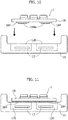
- Figures 12 and 13 exemplify the possibility, already mentioned in the foregoing, of transferring one or more implementation features exemplified herein with reference to one of the annexed Figures to embodiments exemplified in different Figures, while highlighting the possibility of using any number of electrically conductive lines 12.
- Figures 12 and 13 refer to the possibility of using three electrically conductive lines 12, according to a solution which may be used e.g. in the production of lighting devices offering the possibility of varying the colour temperature of a light-coloured (e.g. "white”) lighting radiation, e.g. by implementing a colour regulating function on the radiation emitted by a system which includes single sources emitting radiations with different colours, e.g. according to an RGB pattern.
- a light-coloured e.g. "white”
- the use of a number N>3 of electrically conductive lines 12 leads e.g. to the implementation of a data transmission function to and from the single sources L, e.g. a function of individual selective addressing of each source L.
- Figures 12 and 13 exemplify the possibility, in one or more embodiments, of embedding electrically conductive lines 12 into the channel-shaped body of housing 10, by associating electrically insulating masses 122 to the electrically conductive lines 12, e.g. by originating a sandwich structure which may be arranged in the channel-shaped cavities provided in housing 10, e.g. in the bottom or core wall thereof.
- the electrical contact between sources L and lines 12 may be implemented with contacts 180 which penetrate the insulating layer of the sandwich and reach the conductive layer ("rail") 12.
- Figure 13 shows a source L electrically connected to the two "external" rails 12 among the three rails shown, while the central rail extends below said source and is therefore insulated, i.e. without electrical contact therewith.
- Said central rail may on the other hand be electrically connected to another source L: in this way it is possible to selectively activate the various sources L according to the application needs.
- one and the same channel-shaped housing with a plurality of integrated conductive rails may be used for various supply voltages (e.g. 12 V, 24 V or 48 V) while preserving a satisfactory electrical insulation.
- One or more embodiments may therefore concern a housing (e.g. 10) for lighting devices, the housing including an electrically insulating channel-shaped elongated body, with a plurality of electrically conductive lines (e.g. 12) which extend along the length of said channel-shaped body, said electrically conductive lines being embedded in said channel-shaped body.
- a housing e.g. 10
- the housing including an electrically insulating channel-shaped elongated body, with a plurality of electrically conductive lines (e.g. 12) which extend along the length of said channel-shaped body, said electrically conductive lines being embedded in said channel-shaped body.
- said electrically conductive lines may extend in the central portion of said channel-shaped body.
- said electrically conductive lines may include electrically conductive lines of:
- said electrically conductive lines may have:
- said electrically conductive lines may have an electrically conductive lining (e.g. 120) emerging at the surface of said electrically insulating channel-shaped body.
- a lighting device may include:
- said electrical contact formations may include:
- One or more embodiments may include at least one sealing mass (e.g. 14) sealingly enclosing said at least one light radiation source module in said housing.
- said at least one light radiation source module may include a LED light radiation source.
- a method for making a lighting device may include:
Landscapes
- Engineering & Computer Science (AREA)
- General Engineering & Computer Science (AREA)
- Non-Portable Lighting Devices Or Systems Thereof (AREA)
- Arrangement Of Elements, Cooling, Sealing, Or The Like Of Lighting Devices (AREA)
Abstract
Description
- The description relates to lighting devices.
- One or more embodiments may refer to lighting devices employing electrically-powered light radiation sources, such as solid-state sources, e.g. LED sources.
- One or more embodiments may find application in the implementation of LED modules which are protected against the penetration of foreign agents, e.g. having an IP degree protection.
- Lighting devices such as LED modules, e.g. having an elongated (linear) shape and optionally being flexible, may offer a high level of flexibility as regards installation: as a matter of fact, final users may cut, from a continuous reel, strips of desired lengths according to the application and usage needs.
- Desirable features in such modules are a protection against foreign agents (e.g. an IP degree protection) and/or mechanical flexibility, in order to meet different installation needs, as well as flexibility in lumen output.
- In order to implement protected linear LED modules, the modules may be initially provided without protection, i.e. without sealing, and may subsequently be treated in different ways according to the protection degree to be achieved.
- Exemplary possible solutions are the following:
- a surface lacquering or covering (e.g. via a surface injection of protective material),
- the insertion of LED modules into a protective tube,
- an overall injection around the module, and/or
- the introduction of a potting mass into a protective tube.
- These solutions may be disadvantageous because they may require different layout designs, e.g. when different LEDs are intended to be used and/or different LED pitches must be implemented.
- Moreover, such modules may exhibit a satisfactory bendability only in one plane, e.g. perpendicular to the laminar support structure, which may be implemented e.g. as a Flexible Printed Circuit (FPC).
- In addition, the ohmic resistance of the electrically conductive lines (e.g. copper lines) used for supplying the driving voltage along the LED module may impose limits on the maximum length of the LED module. These electrically conductive lines may have thicknesses limited to standard values (e.g. 35-50 µm: 1 µm = 10-6 m), their width being adapted to be reduced in some points due to design constraints.
- Other solutions have also been proposed based on standard flat cables, as normally used in various electrical devices, whereon there may be arranged mounting locations for LEDs and other electronic components via engravings into the insulating material, the electrical connection between the LEDs and the supply cables being achieved by uncovering the copper wires in certain dedicated areas.
- In such solutions, an IP degree protection may be obtained by inserting the system into a protective tube, or covering the electronic components with protective materials.
- For example, a standard flat cable may be used for the mains voltage supply, and a shrinkable sleeve may act as a protective tube. In other solutions, a standard flat cable may be used for data transmission, while the protection may be achieved through and injection/covering of protective material.
- For example, document
DE 102013203666 A1 describes a multi-wire flat cable, wherein the locations for LEDs and electronic components are obtained by removing insulating material. - Document
US 6 914 194 B2 describes a flat two-wire cable, wherein the locations for LEDs and electronic components are obtained by removing insulating material. The IP protection is achieved by insertion into a transparent sheath. - The main disadvantages of such solutions reside in the implementation complexity as regards manufacturing and costs connected with the production of flat cables, e.g. with CNC machines, as well as in the complexity of the mounting process of the electronic components.
- One or more embodiments aim at overcoming the previously outlined drawbacks.
- According to one or more embodiments, said object may be achieved thanks to a housing for lighting devices having the features set forth in the claims that follow.
- One or more embodiments may also concern a corresponding lighting device, as well as a corresponding method.
- The claims are an integral part of the technical teachings provided herein with reference to the embodiments of the present specification.
- One or more embodiments envisage the use of profiled elements of polymeric materials (e.g. silicone or other polymers) having a channel-shaped or U-shaped profile, wherein there are integrated flexible cables or flat conductors adapted to distribute an electrical supply and/or other electrical signals (e.g. for driving the light radiation sources).
- Along said profiled element it is then possible to arrange, virtually at any position, single light radiation sources, such as Printed Circuit Boards (PCBs) provided with LEDs, e.g. of the type Chip on Board (CoB) or the like.
- In one or more embodiments, it is therefore possible to provide a virtually free spacing pitch of the light radiation sources, with different possible implementations as regards e.g. the establishment of the electrical contact with the conductors integrated in the housing.
- One or more embodiments may achieve an IP degree protection, e.g. via a sealing or potting mass e.g. of a transparent material.
- One or more embodiments may lead to the achievement of one or more of the following advantages:
- for the distribution of the supply voltage along the module it is possible to use electrically conductive rails which are integrated in the module itself; in this way, the module may be cut to a desired length according to the application and usage needs, without relevant limitations as regards higher lengths: the electrical resistance of such electrically conductive rails may actually be lower than that of electrically conductive strips or lines, e.g. made of copper, which may be present e.g. on a flexible printed circuit,
- single light radiation sources (e.g. small LED modules or the like) may be arranged practically at any position in a channel-shaped or U-shaped housing; this leads to the implementation of solutions with a "free" pitch of the light radiation sources, the possibility being given e.g. of changing said pitch along the lengthwise extension of the LED module,
- the portions of a LED module between two adjoining light radiation sources may exhibit high flexibility, which enables e.g. to bend the LED module practically in any direction,
- the LED module may be cut virtually at any position between two adjoining light radiation sources,
- it is possible to use different light radiation sources with the same channel-shaped housing, thus reducing development costs and implementation times of new products,
- it is possible to mix different types of light radiation sources on the same (e.g. LED) module,
- the thermal behaviour is improved with respect to the modules employing a standard FPC circuit treated with a potting mass,
- for specific applications it is possible to add e.g. three or more conductive rails, which leads to the achievement of a LED module having e.g. individually addressable sources, a tunable colour temperature and/or RGB modules, and so on,
- the same channel-shaped housing with integrated conductive rails may be used for various supply voltages (e.g. 12 V, 24 V or 48 V), while preserving a satisfactory electrical insulation level also in the presence of a direct AC supply from the mains,
- the manufacturing costs of LED modules may be decreased, e.g. thanks to the possibility of using standard rigid boards to implement the single light radiation sources,
- the (e.g. IP degree) protection is favoured by the manufacturing process and by the use of connectors and end caps having IP sealing properties, similarly to what is currently used for protected and diffuse LED modules.
- One or more embodiments will now be described, by way of non-limiting example only, with reference to the annexed Figures, wherein:
-
Figures 1 to 3 show housings for lighting devices according to one or more embodiments, -
Figures 4 and 5 show possible usages of housings according to one or more embodiments, -
Figures 6 and 7 exemplify the mounting of light radiation sources onto housings according to one or more embodiments, -
Figures 8 and 9 exemplify the mounting of light radiation sources onto housings according to one or more embodiments, -
Figures 10 and 11 exemplify the mounting of light radiation sources onto housings according to one or more embodiments, and -
Figures 12 and 13 exemplify the mounting of light radiation sources onto housings according to one or more embodiments. - It will be appreciated that, for clarity and simplicity of illustration, the various Figures may not be drawn to the same scale.
- In the following description, various specific details are given to provide a thorough understanding of various exemplary embodiments of the present specification. The embodiments may be practiced without one or several specific details, or with other methods, components, materials, etc. In other instances, well-known structures, materials or operations are not shown or described in detail to avoid obscuring various aspects of the embodiments.
- Reference throughout this specification to "one embodiment" or "an embodiment" means that a particular feature, structure, or characteristic described in connection with the embodiment is included in at least one embodiment. Thus, the possible appearances of the phrases "in one embodiment" or "in an embodiment" in various places throughout this specification are not necessarily all referring to the same embodiment. Furthermore, particular features, structures, or characteristics may be combined in any suitable manner in one or more embodiments.
- The headings provided herein are for convenience only, and therefore do not interpret the extent of protection or scope of the embodiments.
-
Figures 1 to 5 show features of one or more embodiments, adapted to integrate electrically conductive (e.g. metal) rails into the body of ahousing 10 of a lighting device adapted to employ electrically-powered light radiation sources L, for example solid-state light radiation sources such as LED sources. - In this respect, it will be appreciated that one or more implementation features exemplified herein with reference to one of the annexed Figures may be transferred to embodiments shown in different Figures.
- In one or more embodiments,
housing 10 may be a channel-shaped housing, i.e. a housing of elongated shape (and virtually of indefinite length, and optionally adapted to be cut to length according to the application and usage needs) having a U-shaped cross section. - In one or more embodiments,
housing 10 may include electrically insulating, optionally flexible material, such as a silicone polymer. - As better detailed in the following, in one or more embodiments one or more light radiation sources L may be arranged freely along the lengthwise extension of
housing 10, virtually at any position. - In one or more embodiments, the light radiation source(s) L may include LED modules, e.g. according to the techniques known as Chip-on-Board (CoB) or Pin-Through-Hole.
- In one or more embodiments,
housing 10 may be provided, e.g. at the core or central wall thereof, with electricallyconductive lines 12 adapted to have e.g. a flattened shape (see for exampleFigure 1 ) or a circular section (see e.g.Figure 2 ). - In both cases, the electrically
conductive lines 12 may either have a solid structure or comprise stranded wires. - In one or more embodiments, the electrically
conductive lines 12 may be integrally embedded into the material ofhousing 10, or they may be embedded (as exemplified inFigure 3 ) into masses of an electrically conductive material (e.g. a polymer) 120 which emerge at the surface ofhousing 10, e.g. at the bottom wall, within the channel shape or U shape ofhousing 10. - In one or more embodiments (and as further detailed in the following) the electrical contact between electrically
conductive lines 12 and light radiation sources L may be established according to different solutions (sharp piercing contacts, forkshaped contacts, electrically conductive glue drops, etc.). - In one or more embodiments, the number of electrically
conductive lines 12 may be chosen at will. One or more embodiments, as exemplified inFigures 1 to 5 , refer to possible solutions having two electricallyconductive lines 12 adapted to act, e.g., as lines for distributing a supply voltage (e.g. a direct voltage) to light radiation sources L. - One or more embodiments may envisage a different number of
lines 12, e.g. a higher number such as threelines 12 or more; this may be the case, for instance, if the light radiation sources require a control action (e.g. a dimming function) and/or a feedback function on the temperature reached by the sources in operation. - In one or more embodiments, the structure of the obtained lighting device (adapted to be comprised e.g. of a so-called flexible or "flex" LED module) may be rounded off with the provision of a
potting mass 14 introduced into the cavity of the channel shape ofhousing 10. - Therefore, one or more embodiments may achieve (e.g. through a chemical adhesion to the polymeric material of profiled housing 10) a protection of
device 10 against the penetration of foreign agents, e.g. an IP degree protection. -
Figures 6 and 7 show the possibility of establishing the electrical contact between the light radiation source(s) L and the electricallyconductive lines 12 by resorting, for mounting the light radiation source(s) L, to a structure including e.g. a support board 18 (substantially similar to a Printed Circuit Board, PCB) which hosts, e.g. on the face ofboard 18 opposite the face mounting the light radiation source(s) L, sharpelectrical contacts 180. - In one or more embodiments, when the or each light radiation source L is inserted into the channel-shaped
housing 10, contacts 180 (which, through electrically conductive lines provided insupport 18, are connected to the light radiation source(s) L) may penetrate through the material (e.g. silicone) ofhousing 10, so as to establish a contact, optionally exerting a piercing action (seeFigure 7 ) on electricallyconductive lines 12, which are exemplified herein as flattened rails. -
Figures 8 and 9 exemplify (according to solutions substantially similar toFigures 6 and 7 ) the possibility of providing the electrical contact between the light radiation source(s) L and the electricallyconductive lines 12 by resorting to contacts 182 (which may be carried byboard 18 which mounts sources L) having a general fork-like shape. - When the or each light radiation source L is inserted into the channel-shaped
housing 10, theforkshaped contacts 182 may penetrate into the material ofhousing 10 and are adapted, thanks to their fork-like shape, to "surround" the electrically conductive lines 12 (seeFigure 9 ) . - One or more embodiments, as exemplified in
Figures 8 and 9 , may make use of electricallyconductive lines 12 having an at least approximately circular cross-section, adapted to be surrounded by the fork-like shape ofcontacts 182. - Once again it is to be highlighted that, irrespective of the implementation details (e.g. as regards the shape of the cross section) the electrically
conductive lines 12 may be implemented either in solid form or as stranded conductors. -
Figures 10 and 11 exemplify, once again in the same sequence asFigures 6 and 7 as well as 8 and 9, one or more embodiments wherein the electricallyconductive lines 12 are embedded (optionally through a co-extrusion process) into electrically conductive masses (e.g. an electrically conductive polymeric material) extending around the electricallyconductive lines 12. - Moreover, the electrically
conductive masses 120 embeddinglines 12 may emerge at the bottom or central wall of channel-shapedhousing 10. - In this case, the electrical contact with the light radiation source(s) may be obtained via electrical contact lands 184 provided on
board 18, e.g. on the face opposite the face which mounts light radiation source(s) L, with masses of electrically conductive (e.g. adhesive)material 184a located between thelands 184 and the electricallyconductive masses 120. -
Material 120 and adhesive 184 may contribute to impart the implemented electrical contact with an ohmic resistance higher than the ohmic resistance which may be obtained through e.g. metal contacts. The fact that such a connection originates a certain ohmic resistance (in series) may be considered negligible, because at any rate (e.g. in the case ofadhesive layer 184a) it is a thin layer which is sandwiched between conductive materials having a rather large exposed surface. -
Figures 12 and 13 exemplify the possibility, already mentioned in the foregoing, of transferring one or more implementation features exemplified herein with reference to one of the annexed Figures to embodiments exemplified in different Figures, while highlighting the possibility of using any number of electricallyconductive lines 12. - For example,
Figures 12 and 13 refer to the possibility of using three electricallyconductive lines 12, according to a solution which may be used e.g. in the production of lighting devices offering the possibility of varying the colour temperature of a light-coloured (e.g. "white") lighting radiation, e.g. by implementing a colour regulating function on the radiation emitted by a system which includes single sources emitting radiations with different colours, e.g. according to an RGB pattern. - The use of a number N>3 of electrically
conductive lines 12 leads e.g. to the implementation of a data transmission function to and from the single sources L, e.g. a function of individual selective addressing of each source L. -
Figures 12 and 13 exemplify the possibility, in one or more embodiments, of embedding electricallyconductive lines 12 into the channel-shaped body ofhousing 10, by associating electrically insulatingmasses 122 to the electricallyconductive lines 12, e.g. by originating a sandwich structure which may be arranged in the channel-shaped cavities provided inhousing 10, e.g. in the bottom or core wall thereof. - As exemplified in dashed lines in
Figure 13 , the electrical contact between sources L and lines 12 may be implemented withcontacts 180 which penetrate the insulating layer of the sandwich and reach the conductive layer ("rail") 12. - This may take place according to different solutions for the various sources L. For example,
Figure 13 shows a source L electrically connected to the two "external" rails 12 among the three rails shown, while the central rail extends below said source and is therefore insulated, i.e. without electrical contact therewith. - Said central rail may on the other hand be electrically connected to another source L: in this way it is possible to selectively activate the various sources L according to the application needs.
- Moreover, in one or more embodiments, one and the same channel-shaped housing with a plurality of integrated conductive rails may be used for various supply voltages (e.g. 12 V, 24 V or 48 V) while preserving a satisfactory electrical insulation.
- One or more embodiments may therefore concern a housing (e.g. 10) for lighting devices, the housing including an electrically insulating channel-shaped elongated body, with a plurality of electrically conductive lines (e.g. 12) which extend along the length of said channel-shaped body, said electrically conductive lines being embedded in said channel-shaped body.
- In one or more embodiments, said electrically conductive lines may extend in the central portion of said channel-shaped body.
- In one or more embodiments, said electrically conductive lines may include electrically conductive lines of:
- a flat shape, and/or
- a circular shape.
- In one or more embodiments, said electrically conductive lines may have:
- a solid structure, or
- a stranded structure.
- In one or more embodiments, said electrically conductive lines may have an electrically conductive lining (e.g. 120) emerging at the surface of said electrically insulating channel-shaped body.
- In one or more embodiments, a lighting device may include:
- a housing according to one or more embodiments,
- at least one electrically-powered light radiation source module (e.g. L, 18) arranged in said housing, said module being provided with electrical contact formations (e.g. 180, 182, 184) with said electrically conductive lines.
- In one or more embodiments, said electrical contact formations may include:
- sharp contacts (e.g. 180) adapted to penetrate into said channel-shaped body for establishing a contact with said electrically conductive lines, and/or
- fork-like contact formations (e.g. 182) adapted to penetrate into said channel-shaped body for establishing a contact with said electrically conductive lines, by being arranged astride said electrically conductive lines, and/or
- contact lands (e.g. 184) to make contact adhesion (e.g. 184a) with the electrically conductive linings of said electrically conductive lines emerging at the surface of said electrically insulating channel-shaped body.
- One or more embodiments may include at least one sealing mass (e.g. 14) sealingly enclosing said at least one light radiation source module in said housing.
- In one or more embodiments, said at least one light radiation source module may include a LED light radiation source.
- In one or more embodiments, a method for making a lighting device may include:
- providing a housing according to one or more embodiments,
- arranging in said housing at least one electrically-powered light radiation source module; said module being provided with electrical contact formations with said electrically conductive lines and optionally including a LED light radiation source.
- Without prejudice to the basic principles, the details and the embodiments may vary, even appreciably, with respect to what has been described herein by way of non-limiting example only, without departing from the extent of protection.
- The extent of protection is defined by the annexed claims.
Claims (10)
- A housing (10) for lighting devices, the housing (10) including an electrically insulating channel-shaped elongated body, with a plurality of electrically conductive lines (12) which extend along the length of said channel-shaped body (10) said electrically conductive lines (12) embedded in said channel-shaped body.
- The housing (10) of claim 1, wherein said electrically conductive lines (12) extend in the central portion of said channel-shaped body.
- The housing (10) of claim 1 or claim 2, wherein said electrically conductive lines (12) include electrically conductive lines of:- a flat shape, and/or- a circular shape.
- The housing (10) of any of the preceding claims, wherein said electrically conductive lines (12) have:- a solid structure, or- a stranded structure.
- The housing (10) of any of the preceding claims, wherein said electrically conductive lines (12) have an electrically conductive lining (120) emerging at the surface of said electrically insulating channel-shaped body.
- A lighting device, including:- a housing (10) according to any of claims 1 to 5,- at least one electrically-powered light radiation source module (L, 18) arranged in said housing (10), said module (L, 18) being provided with electrical contact formations (180, 182, 184) with said electrically conductive lines (12).
- The lighting device of claim 6, wherein said electrical contact formations include:- sharp contacts (180) to penetrate into said channel-shaped body (10) for making contact with said electrically conductive lines (12), and/or- fork-like contact formations (182) to penetrate into said channel-shaped body (10) for making contact with said electrically conductive lines (12) by being arranged astride said electrically conductive lines (12), and/or- contact lands (184) to make contact adhesion (184a) to electrically conductive linings (120) of said electrically conductive lines (12) emerging at the surface of said electrically insulating channel-shaped body.
- The lighting device of claim 6 or claim 7, including at least one sealing mass (14) sealingly enclosing said at least one light radiation source module (L, 18) in said housing (10).
- The lighting device of any of claims 6 to 8, wherein said at least one light radiation source module (L, 18) includes a LED light radiation source.
- A process for making a lighting device, the method including:- providing a housing (10) according to any of claims 1 to 5,- arranging in said housing (10) at least one electrically-powered light radiation source module (L, 18); said module (L, 18) provided with electrical contact formations (180, 182, 184) with said electrically conductive lines (12) and preferably including a LED radiation source.
Applications Claiming Priority (1)
| Application Number | Priority Date | Filing Date | Title |
|---|---|---|---|
| IT201600072576 | 2016-07-12 |
Publications (2)
| Publication Number | Publication Date |
|---|---|
| EP3270053A1 true EP3270053A1 (en) | 2018-01-17 |
| EP3270053B1 EP3270053B1 (en) | 2019-05-01 |
Family
ID=57796811
Family Applications (1)
| Application Number | Title | Priority Date | Filing Date |
|---|---|---|---|
| EP17180022.0A Not-in-force EP3270053B1 (en) | 2016-07-12 | 2017-07-06 | A housing for lighting devices, corresponding lighting device and method |
Country Status (2)
| Country | Link |
|---|---|
| US (1) | US20180017238A1 (en) |
| EP (1) | EP3270053B1 (en) |
Cited By (2)
| Publication number | Priority date | Publication date | Assignee | Title |
|---|---|---|---|---|
| DE102016012639B4 (en) | 2016-10-24 | 2018-09-20 | Nicola Barthelme | Chainable, fully encapsulated, flexible light emitting diode strip and method for its production |
| EP3561369A1 (en) | 2018-04-24 | 2019-10-30 | CLD Germany GmbH | Fully cast flexible light emitting diode strip for large feed-in stretching and method for producing the same |
Families Citing this family (5)
| Publication number | Priority date | Publication date | Assignee | Title |
|---|---|---|---|---|
| US10738976B1 (en) * | 2017-10-27 | 2020-08-11 | Shanghai Sansi Electronic Engineering Co., Ltd. | Lighting device |
| KR102282199B1 (en) * | 2018-07-17 | 2021-07-27 | 루미리즈 홀딩 비.브이. | Lighting device comprising LEDs and a reflective element |
| CN209084477U (en) * | 2018-07-23 | 2019-07-09 | 上犹县嘉亿灯饰制品有限公司 | Headlamp and ornament lamp |
| CN113739093A (en) * | 2020-05-28 | 2021-12-03 | 漳州立达信光电子科技有限公司 | Bar lamp |
| IT202200024021A1 (en) * | 2022-11-22 | 2024-05-22 | Simes | LIGHTING SYSTEM |
Citations (5)
| Publication number | Priority date | Publication date | Assignee | Title |
|---|---|---|---|---|
| WO2001025681A1 (en) * | 1999-10-04 | 2001-04-12 | Hutchins Nicolas D | Elongated light emitting diode lighting system |
| KR20090012846A (en) * | 2007-07-31 | 2009-02-04 | 박효숙 | LED module |
| DE102009008845A1 (en) * | 2009-02-13 | 2010-08-26 | Osram Gesellschaft mit beschränkter Haftung | Light module and method for producing a light module |
| WO2013094833A1 (en) * | 2011-12-20 | 2013-06-27 | Han Yoon-Hee | Optical led module and method of manufacturing optical led module |
| US20150369459A1 (en) * | 2014-06-18 | 2015-12-24 | General Led, Inc. | Busline LED Module |
Family Cites Families (2)
| Publication number | Priority date | Publication date | Assignee | Title |
|---|---|---|---|---|
| GB9221706D0 (en) * | 1992-10-15 | 1992-12-02 | Raychem Sa Nv | Repair of damaged electrode in impressed current corrosion protection system |
| TWI442000B (en) * | 2011-07-19 | 2014-06-21 | Wistron Corp | Light bar structure and light source device |
-
2017
- 2017-07-05 US US15/641,365 patent/US20180017238A1/en not_active Abandoned
- 2017-07-06 EP EP17180022.0A patent/EP3270053B1/en not_active Not-in-force
Patent Citations (5)
| Publication number | Priority date | Publication date | Assignee | Title |
|---|---|---|---|---|
| WO2001025681A1 (en) * | 1999-10-04 | 2001-04-12 | Hutchins Nicolas D | Elongated light emitting diode lighting system |
| KR20090012846A (en) * | 2007-07-31 | 2009-02-04 | 박효숙 | LED module |
| DE102009008845A1 (en) * | 2009-02-13 | 2010-08-26 | Osram Gesellschaft mit beschränkter Haftung | Light module and method for producing a light module |
| WO2013094833A1 (en) * | 2011-12-20 | 2013-06-27 | Han Yoon-Hee | Optical led module and method of manufacturing optical led module |
| US20150369459A1 (en) * | 2014-06-18 | 2015-12-24 | General Led, Inc. | Busline LED Module |
Cited By (3)
| Publication number | Priority date | Publication date | Assignee | Title |
|---|---|---|---|---|
| DE102016012639B4 (en) | 2016-10-24 | 2018-09-20 | Nicola Barthelme | Chainable, fully encapsulated, flexible light emitting diode strip and method for its production |
| EP3561369A1 (en) | 2018-04-24 | 2019-10-30 | CLD Germany GmbH | Fully cast flexible light emitting diode strip for large feed-in stretching and method for producing the same |
| WO2019206457A1 (en) | 2018-04-24 | 2019-10-31 | Cld Germany Gmbh | Fully potted, flexible light-emitting diode strip for large feed-in lines and method for producing said light-emitting diode strip |
Also Published As
| Publication number | Publication date |
|---|---|
| US20180017238A1 (en) | 2018-01-18 |
| EP3270053B1 (en) | 2019-05-01 |
Similar Documents
| Publication | Publication Date | Title |
|---|---|---|
| EP3270053B1 (en) | A housing for lighting devices, corresponding lighting device and method | |
| EP2716959B1 (en) | Light emitting device | |
| DE102016012639B4 (en) | Chainable, fully encapsulated, flexible light emitting diode strip and method for its production | |
| JP5031011B2 (en) | Flexible light emitting device and manufacturing method thereof | |
| US20020110000A1 (en) | Lighting device | |
| EP1908150B1 (en) | Led string light engine | |
| US9425370B2 (en) | Method for producing a striplight and striplight | |
| EP1965123B1 (en) | Lighting apparatus cable and lighting apparatus using the same | |
| EP2474775B1 (en) | Integrally formed single piece light emitting diode light wire and uses thereof | |
| US9638380B2 (en) | Bendable LED strip | |
| EP3314163B1 (en) | A lighting device and corresponding method | |
| US20050146870A1 (en) | Elongated flexible lighting equipment and fabricating method of same | |
| DE102013203666B4 (en) | Luminous band with band-shaped substrate | |
| US20130034988A1 (en) | Electrical connector for flexible led strip seal | |
| US9324928B2 (en) | Lighting device and corresponding method | |
| HUE029075T2 (en) | Connector for moisture-proof electric plug-in connector | |
| US20160334090A1 (en) | Connector for lighting devices and corresponding method | |
| DE102016121047A1 (en) | LIGHTING DEVICE FOR A VEHICLE AND MANUFACTURING METHOD FOR A LIGHTING DEVICE | |
| WO2007041805A1 (en) | Elongate lighting means | |
| EP3115688B1 (en) | A lighting device and corresponding method | |
| EP3664587A1 (en) | Electronic device and manufacturing method thereof | |
| SE8104399L (en) | ELECTRICAL ELECTRICAL CABLE OF MULTIPLE CONDUCTOR AND SET FOR ITS MANUFACTURING | |
| EP3146255B1 (en) | Illuminant comprising an led | |
| KR20080081538A (en) | Light emitting device | |
| DE202010007036U1 (en) | Carrier profile for a lighting |
Legal Events
| Date | Code | Title | Description |
|---|---|---|---|
| PUAI | Public reference made under article 153(3) epc to a published international application that has entered the european phase |
Free format text: ORIGINAL CODE: 0009012 |
|
| STAA | Information on the status of an ep patent application or granted ep patent |
Free format text: STATUS: THE APPLICATION HAS BEEN PUBLISHED |
|
| AK | Designated contracting states |
Kind code of ref document: A1 Designated state(s): AL AT BE BG CH CY CZ DE DK EE ES FI FR GB GR HR HU IE IS IT LI LT LU LV MC MK MT NL NO PL PT RO RS SE SI SK SM TR |
|
| AX | Request for extension of the european patent |
Extension state: BA ME |
|
| RAP1 | Party data changed (applicant data changed or rights of an application transferred) |
Owner name: OSRAM S.P.A. - SOCIETA' RIUNITE OSRAM EDISON CLERI Owner name: OSRAM GMBH |
|
| STAA | Information on the status of an ep patent application or granted ep patent |
Free format text: STATUS: REQUEST FOR EXAMINATION WAS MADE |
|
| 17P | Request for examination filed |
Effective date: 20180709 |
|
| RBV | Designated contracting states (corrected) |
Designated state(s): AL AT BE BG CH CY CZ DE DK EE ES FI FR GB GR HR HU IE IS IT LI LT LU LV MC MK MT NL NO PL PT RO RS SE SI SK SM TR |
|
| GRAP | Despatch of communication of intention to grant a patent |
Free format text: ORIGINAL CODE: EPIDOSNIGR1 |
|
| STAA | Information on the status of an ep patent application or granted ep patent |
Free format text: STATUS: GRANT OF PATENT IS INTENDED |
|
| RIC1 | Information provided on ipc code assigned before grant |
Ipc: F21Y 103/10 20160101ALN20181023BHEP Ipc: H01R 12/67 20110101ALI20181023BHEP Ipc: F21Y 101/00 20160101ALN20181023BHEP Ipc: H01R 4/2404 20180101ALI20181023BHEP Ipc: F21S 4/22 20160101ALI20181023BHEP Ipc: F21V 31/04 20060101ALN20181023BHEP Ipc: F21Y 115/10 20160101ALN20181023BHEP Ipc: H01R 4/2416 20180101ALI20181023BHEP Ipc: F21V 21/002 20060101AFI20181023BHEP |
|
| INTG | Intention to grant announced |
Effective date: 20181204 |
|
| GRAS | Grant fee paid |
Free format text: ORIGINAL CODE: EPIDOSNIGR3 |
|
| GRAA | (expected) grant |
Free format text: ORIGINAL CODE: 0009210 |
|
| STAA | Information on the status of an ep patent application or granted ep patent |
Free format text: STATUS: THE PATENT HAS BEEN GRANTED |
|
| AK | Designated contracting states |
Kind code of ref document: B1 Designated state(s): AL AT BE BG CH CY CZ DE DK EE ES FI FR GB GR HR HU IE IS IT LI LT LU LV MC MK MT NL NO PL PT RO RS SE SI SK SM TR |
|
| REG | Reference to a national code |
Ref country code: GB Ref legal event code: FG4D |
|
| REG | Reference to a national code |
Ref country code: CH Ref legal event code: EP Ref country code: AT Ref legal event code: REF Ref document number: 1127415 Country of ref document: AT Kind code of ref document: T Effective date: 20190515 |
|
| REG | Reference to a national code |
Ref country code: DE Ref legal event code: R096 Ref document number: 602017003615 Country of ref document: DE |
|
| REG | Reference to a national code |
Ref country code: IE Ref legal event code: FG4D |
|
| REG | Reference to a national code |
Ref country code: NL Ref legal event code: MP Effective date: 20190501 |
|
| REG | Reference to a national code |
Ref country code: LT Ref legal event code: MG4D |
|
| PG25 | Lapsed in a contracting state [announced via postgrant information from national office to epo] |
Ref country code: NL Free format text: LAPSE BECAUSE OF FAILURE TO SUBMIT A TRANSLATION OF THE DESCRIPTION OR TO PAY THE FEE WITHIN THE PRESCRIBED TIME-LIMIT Effective date: 20190501 Ref country code: SE Free format text: LAPSE BECAUSE OF FAILURE TO SUBMIT A TRANSLATION OF THE DESCRIPTION OR TO PAY THE FEE WITHIN THE PRESCRIBED TIME-LIMIT Effective date: 20190501 Ref country code: LT Free format text: LAPSE BECAUSE OF FAILURE TO SUBMIT A TRANSLATION OF THE DESCRIPTION OR TO PAY THE FEE WITHIN THE PRESCRIBED TIME-LIMIT Effective date: 20190501 Ref country code: ES Free format text: LAPSE BECAUSE OF FAILURE TO SUBMIT A TRANSLATION OF THE DESCRIPTION OR TO PAY THE FEE WITHIN THE PRESCRIBED TIME-LIMIT Effective date: 20190501 Ref country code: FI Free format text: LAPSE BECAUSE OF FAILURE TO SUBMIT A TRANSLATION OF THE DESCRIPTION OR TO PAY THE FEE WITHIN THE PRESCRIBED TIME-LIMIT Effective date: 20190501 Ref country code: AL Free format text: LAPSE BECAUSE OF FAILURE TO SUBMIT A TRANSLATION OF THE DESCRIPTION OR TO PAY THE FEE WITHIN THE PRESCRIBED TIME-LIMIT Effective date: 20190501 Ref country code: PT Free format text: LAPSE BECAUSE OF FAILURE TO SUBMIT A TRANSLATION OF THE DESCRIPTION OR TO PAY THE FEE WITHIN THE PRESCRIBED TIME-LIMIT Effective date: 20190901 Ref country code: HR Free format text: LAPSE BECAUSE OF FAILURE TO SUBMIT A TRANSLATION OF THE DESCRIPTION OR TO PAY THE FEE WITHIN THE PRESCRIBED TIME-LIMIT Effective date: 20190501 Ref country code: NO Free format text: LAPSE BECAUSE OF FAILURE TO SUBMIT A TRANSLATION OF THE DESCRIPTION OR TO PAY THE FEE WITHIN THE PRESCRIBED TIME-LIMIT Effective date: 20190801 |
|
| PG25 | Lapsed in a contracting state [announced via postgrant information from national office to epo] |
Ref country code: GR Free format text: LAPSE BECAUSE OF FAILURE TO SUBMIT A TRANSLATION OF THE DESCRIPTION OR TO PAY THE FEE WITHIN THE PRESCRIBED TIME-LIMIT Effective date: 20190802 Ref country code: LV Free format text: LAPSE BECAUSE OF FAILURE TO SUBMIT A TRANSLATION OF THE DESCRIPTION OR TO PAY THE FEE WITHIN THE PRESCRIBED TIME-LIMIT Effective date: 20190501 Ref country code: BG Free format text: LAPSE BECAUSE OF FAILURE TO SUBMIT A TRANSLATION OF THE DESCRIPTION OR TO PAY THE FEE WITHIN THE PRESCRIBED TIME-LIMIT Effective date: 20190801 Ref country code: RS Free format text: LAPSE BECAUSE OF FAILURE TO SUBMIT A TRANSLATION OF THE DESCRIPTION OR TO PAY THE FEE WITHIN THE PRESCRIBED TIME-LIMIT Effective date: 20190501 |
|
| REG | Reference to a national code |
Ref country code: AT Ref legal event code: MK05 Ref document number: 1127415 Country of ref document: AT Kind code of ref document: T Effective date: 20190501 |
|
| PG25 | Lapsed in a contracting state [announced via postgrant information from national office to epo] |
Ref country code: IS Free format text: LAPSE BECAUSE OF FAILURE TO SUBMIT A TRANSLATION OF THE DESCRIPTION OR TO PAY THE FEE WITHIN THE PRESCRIBED TIME-LIMIT Effective date: 20190901 |
|
| PG25 | Lapsed in a contracting state [announced via postgrant information from national office to epo] |
Ref country code: AT Free format text: LAPSE BECAUSE OF FAILURE TO SUBMIT A TRANSLATION OF THE DESCRIPTION OR TO PAY THE FEE WITHIN THE PRESCRIBED TIME-LIMIT Effective date: 20190501 Ref country code: DK Free format text: LAPSE BECAUSE OF FAILURE TO SUBMIT A TRANSLATION OF THE DESCRIPTION OR TO PAY THE FEE WITHIN THE PRESCRIBED TIME-LIMIT Effective date: 20190501 Ref country code: EE Free format text: LAPSE BECAUSE OF FAILURE TO SUBMIT A TRANSLATION OF THE DESCRIPTION OR TO PAY THE FEE WITHIN THE PRESCRIBED TIME-LIMIT Effective date: 20190501 Ref country code: CZ Free format text: LAPSE BECAUSE OF FAILURE TO SUBMIT A TRANSLATION OF THE DESCRIPTION OR TO PAY THE FEE WITHIN THE PRESCRIBED TIME-LIMIT Effective date: 20190501 Ref country code: RO Free format text: LAPSE BECAUSE OF FAILURE TO SUBMIT A TRANSLATION OF THE DESCRIPTION OR TO PAY THE FEE WITHIN THE PRESCRIBED TIME-LIMIT Effective date: 20190501 Ref country code: SK Free format text: LAPSE BECAUSE OF FAILURE TO SUBMIT A TRANSLATION OF THE DESCRIPTION OR TO PAY THE FEE WITHIN THE PRESCRIBED TIME-LIMIT Effective date: 20190501 |
|
| REG | Reference to a national code |
Ref country code: DE Ref legal event code: R097 Ref document number: 602017003615 Country of ref document: DE |
|
| PG25 | Lapsed in a contracting state [announced via postgrant information from national office to epo] |
Ref country code: SM Free format text: LAPSE BECAUSE OF FAILURE TO SUBMIT A TRANSLATION OF THE DESCRIPTION OR TO PAY THE FEE WITHIN THE PRESCRIBED TIME-LIMIT Effective date: 20190501 Ref country code: IT Free format text: LAPSE BECAUSE OF FAILURE TO SUBMIT A TRANSLATION OF THE DESCRIPTION OR TO PAY THE FEE WITHIN THE PRESCRIBED TIME-LIMIT Effective date: 20190501 Ref country code: MC Free format text: LAPSE BECAUSE OF FAILURE TO SUBMIT A TRANSLATION OF THE DESCRIPTION OR TO PAY THE FEE WITHIN THE PRESCRIBED TIME-LIMIT Effective date: 20190501 |
|
| PLBE | No opposition filed within time limit |
Free format text: ORIGINAL CODE: 0009261 |
|
| STAA | Information on the status of an ep patent application or granted ep patent |
Free format text: STATUS: NO OPPOSITION FILED WITHIN TIME LIMIT |
|
| PG25 | Lapsed in a contracting state [announced via postgrant information from national office to epo] |
Ref country code: TR Free format text: LAPSE BECAUSE OF FAILURE TO SUBMIT A TRANSLATION OF THE DESCRIPTION OR TO PAY THE FEE WITHIN THE PRESCRIBED TIME-LIMIT Effective date: 20190501 |
|
| 26N | No opposition filed |
Effective date: 20200204 |
|
| REG | Reference to a national code |
Ref country code: BE Ref legal event code: MM Effective date: 20190731 |
|
| PG25 | Lapsed in a contracting state [announced via postgrant information from national office to epo] |
Ref country code: PL Free format text: LAPSE BECAUSE OF FAILURE TO SUBMIT A TRANSLATION OF THE DESCRIPTION OR TO PAY THE FEE WITHIN THE PRESCRIBED TIME-LIMIT Effective date: 20190501 |
|
| PG25 | Lapsed in a contracting state [announced via postgrant information from national office to epo] |
Ref country code: BE Free format text: LAPSE BECAUSE OF NON-PAYMENT OF DUE FEES Effective date: 20190731 Ref country code: LU Free format text: LAPSE BECAUSE OF NON-PAYMENT OF DUE FEES Effective date: 20190706 Ref country code: SI Free format text: LAPSE BECAUSE OF FAILURE TO SUBMIT A TRANSLATION OF THE DESCRIPTION OR TO PAY THE FEE WITHIN THE PRESCRIBED TIME-LIMIT Effective date: 20190501 |
|
| PG25 | Lapsed in a contracting state [announced via postgrant information from national office to epo] |
Ref country code: FR Free format text: LAPSE BECAUSE OF NON-PAYMENT OF DUE FEES Effective date: 20190731 |
|
| PG25 | Lapsed in a contracting state [announced via postgrant information from national office to epo] |
Ref country code: IE Free format text: LAPSE BECAUSE OF NON-PAYMENT OF DUE FEES Effective date: 20190706 |
|
| REG | Reference to a national code |
Ref country code: CH Ref legal event code: PL |
|
| PG25 | Lapsed in a contracting state [announced via postgrant information from national office to epo] |
Ref country code: LI Free format text: LAPSE BECAUSE OF NON-PAYMENT OF DUE FEES Effective date: 20200731 Ref country code: CH Free format text: LAPSE BECAUSE OF NON-PAYMENT OF DUE FEES Effective date: 20200731 |
|
| PG25 | Lapsed in a contracting state [announced via postgrant information from national office to epo] |
Ref country code: CY Free format text: LAPSE BECAUSE OF FAILURE TO SUBMIT A TRANSLATION OF THE DESCRIPTION OR TO PAY THE FEE WITHIN THE PRESCRIBED TIME-LIMIT Effective date: 20190501 |
|
| PG25 | Lapsed in a contracting state [announced via postgrant information from national office to epo] |
Ref country code: MT Free format text: LAPSE BECAUSE OF FAILURE TO SUBMIT A TRANSLATION OF THE DESCRIPTION OR TO PAY THE FEE WITHIN THE PRESCRIBED TIME-LIMIT Effective date: 20190501 Ref country code: HU Free format text: LAPSE BECAUSE OF FAILURE TO SUBMIT A TRANSLATION OF THE DESCRIPTION OR TO PAY THE FEE WITHIN THE PRESCRIBED TIME-LIMIT; INVALID AB INITIO Effective date: 20170706 |
|
| GBPC | Gb: european patent ceased through non-payment of renewal fee |
Effective date: 20210706 |
|
| PG25 | Lapsed in a contracting state [announced via postgrant information from national office to epo] |
Ref country code: GB Free format text: LAPSE BECAUSE OF NON-PAYMENT OF DUE FEES Effective date: 20210706 |
|
| PG25 | Lapsed in a contracting state [announced via postgrant information from national office to epo] |
Ref country code: MK Free format text: LAPSE BECAUSE OF FAILURE TO SUBMIT A TRANSLATION OF THE DESCRIPTION OR TO PAY THE FEE WITHIN THE PRESCRIBED TIME-LIMIT Effective date: 20190501 |
|
| REG | Reference to a national code |
Ref country code: DE Ref legal event code: R081 Ref document number: 602017003615 Country of ref document: DE Owner name: INVENTRONICS GMBH, DE Free format text: FORMER OWNER: OSRAM GMBH, 80807 MUENCHEN, DE |
|
| REG | Reference to a national code |
Ref country code: DE Ref legal event code: R081 Ref document number: 602017003615 Country of ref document: DE Owner name: INVENTRONICS GMBH, DE Free format text: FORMER OWNER: OPTOTRONIC GMBH, 85748 GARCHING, DE |
|
| PGFP | Annual fee paid to national office [announced via postgrant information from national office to epo] |
Ref country code: DE Payment date: 20230731 Year of fee payment: 7 |
|
| REG | Reference to a national code |
Ref country code: DE Ref legal event code: R119 Ref document number: 602017003615 Country of ref document: DE |
|
| PG25 | Lapsed in a contracting state [announced via postgrant information from national office to epo] |
Ref country code: DE Free format text: LAPSE BECAUSE OF NON-PAYMENT OF DUE FEES Effective date: 20250201 |