EP3267646B1 - Module de correction de défaut iq - Google Patents
Module de correction de défaut iq Download PDFInfo
- Publication number
- EP3267646B1 EP3267646B1 EP16178249.5A EP16178249A EP3267646B1 EP 3267646 B1 EP3267646 B1 EP 3267646B1 EP 16178249 A EP16178249 A EP 16178249A EP 3267646 B1 EP3267646 B1 EP 3267646B1
- Authority
- EP
- European Patent Office
- Prior art keywords
- mismatch
- phase
- amplitude
- signal
- sub
- Prior art date
- Legal status (The legal status is an assumption and is not a legal conclusion. Google has not performed a legal analysis and makes no representation as to the accuracy of the status listed.)
- Active
Links
- 238000012937 correction Methods 0.000 title claims description 80
- 238000001514 detection method Methods 0.000 claims description 87
- 230000009466 transformation Effects 0.000 claims description 42
- 230000006870 function Effects 0.000 claims description 33
- 238000000034 method Methods 0.000 claims description 24
- 238000013213 extrapolation Methods 0.000 claims description 18
- 230000004044 response Effects 0.000 claims description 10
- 238000001914 filtration Methods 0.000 claims description 9
- 230000010354 integration Effects 0.000 claims description 9
- 230000000977 initiatory effect Effects 0.000 claims description 8
- 230000008569 process Effects 0.000 claims description 6
- 230000007423 decrease Effects 0.000 claims description 5
- 238000003860 storage Methods 0.000 claims description 5
- 230000001052 transient effect Effects 0.000 claims description 5
- 230000003321 amplification Effects 0.000 claims description 4
- 238000003199 nucleic acid amplification method Methods 0.000 claims description 4
- 238000004590 computer program Methods 0.000 claims description 3
- 238000012545 processing Methods 0.000 description 14
- 238000012546 transfer Methods 0.000 description 12
- 230000008859 change Effects 0.000 description 10
- 238000010586 diagram Methods 0.000 description 10
- 239000011159 matrix material Substances 0.000 description 10
- 230000002238 attenuated effect Effects 0.000 description 6
- 230000000737 periodic effect Effects 0.000 description 6
- 238000004364 calculation method Methods 0.000 description 5
- 238000006243 chemical reaction Methods 0.000 description 5
- 230000004043 responsiveness Effects 0.000 description 4
- 238000013459 approach Methods 0.000 description 3
- 238000012935 Averaging Methods 0.000 description 2
- 238000013461 design Methods 0.000 description 2
- 230000000694 effects Effects 0.000 description 2
- 238000004519 manufacturing process Methods 0.000 description 2
- 239000000463 material Substances 0.000 description 2
- 238000012986 modification Methods 0.000 description 2
- 230000004048 modification Effects 0.000 description 2
- 238000000844 transformation Methods 0.000 description 2
- 230000000903 blocking effect Effects 0.000 description 1
- 239000000969 carrier Substances 0.000 description 1
- 238000010276 construction Methods 0.000 description 1
- 238000011109 contamination Methods 0.000 description 1
- 230000008878 coupling Effects 0.000 description 1
- 238000010168 coupling process Methods 0.000 description 1
- 238000005859 coupling reaction Methods 0.000 description 1
- 230000003247 decreasing effect Effects 0.000 description 1
- 238000012886 linear function Methods 0.000 description 1
- 238000005457 optimization Methods 0.000 description 1
- 230000010355 oscillation Effects 0.000 description 1
- 230000009467 reduction Effects 0.000 description 1
- 238000000926 separation method Methods 0.000 description 1
- 238000007493 shaping process Methods 0.000 description 1
- 238000006467 substitution reaction Methods 0.000 description 1
- 238000013519 translation Methods 0.000 description 1
Images


Classifications
-
- H—ELECTRICITY
- H04—ELECTRIC COMMUNICATION TECHNIQUE
- H04L—TRANSMISSION OF DIGITAL INFORMATION, e.g. TELEGRAPHIC COMMUNICATION
- H04L27/00—Modulated-carrier systems
- H04L27/32—Carrier systems characterised by combinations of two or more of the types covered by groups H04L27/02, H04L27/10, H04L27/18 or H04L27/26
- H04L27/34—Amplitude- and phase-modulated carrier systems, e.g. quadrature-amplitude modulated carrier systems
- H04L27/36—Modulator circuits; Transmitter circuits
- H04L27/362—Modulation using more than one carrier, e.g. with quadrature carriers, separately amplitude modulated
- H04L27/364—Arrangements for overcoming imperfections in the modulator, e.g. quadrature error or unbalanced I and Q levels
-
- H—ELECTRICITY
- H04—ELECTRIC COMMUNICATION TECHNIQUE
- H04L—TRANSMISSION OF DIGITAL INFORMATION, e.g. TELEGRAPHIC COMMUNICATION
- H04L27/00—Modulated-carrier systems
- H04L27/32—Carrier systems characterised by combinations of two or more of the types covered by groups H04L27/02, H04L27/10, H04L27/18 or H04L27/26
- H04L27/34—Amplitude- and phase-modulated carrier systems, e.g. quadrature-amplitude modulated carrier systems
- H04L27/38—Demodulator circuits; Receiver circuits
- H04L27/3845—Demodulator circuits; Receiver circuits using non - coherent demodulation, i.e. not using a phase synchronous carrier
- H04L27/3854—Demodulator circuits; Receiver circuits using non - coherent demodulation, i.e. not using a phase synchronous carrier using a non - coherent carrier, including systems with baseband correction for phase or frequency offset
- H04L27/3863—Compensation for quadrature error in the received signal
-
- H—ELECTRICITY
- H04—ELECTRIC COMMUNICATION TECHNIQUE
- H04L—TRANSMISSION OF DIGITAL INFORMATION, e.g. TELEGRAPHIC COMMUNICATION
- H04L1/00—Arrangements for detecting or preventing errors in the information received
- H04L1/20—Arrangements for detecting or preventing errors in the information received using signal quality detector
Definitions
- This disclosure relates to in-phase/quadrature (IQ) mismatch detection and correction in radio frequency receivers, and in particular, although not exclusively, to an IQ mismatch correction module for a radio frequency receiver.
- IQ in-phase/quadrature
- Modern radio frequency receivers such as those used for wideband data reception, typically comprise both analogue and digital sections in order to efficiently process signals.
- a difficulty found in conventional radio frequency receivers relates to providing the required image rejection properties in an efficient manner.
- US2007080835 (A1 ) relates to a receiver that aims to reject image signals with higher accuracy over wider frequency band.
- the receiver can be provided as a low IF receiver by inputting a calibration signal of frequency before reception of signals and determining the frequency response of a calibrating filter in a filter mismatch calibrating circuit to make zero amplitude and phase mismatches between the I component and Q component of the quadrature demodulation signal at the frequency.
- an IQ mismatch correction module for a radio receiver, the IQ mismatch correction module comprising:
- the input signal may be a digital domain signal.
- the IQ mismatch correction module may comprise a plurality of bandpass filters. Each of the plurality of bandpass filters may be configured to pass a respective sub-band of the plurality of sub-bands in order to provide the bandpass filtered signals from the plurality of sub-bands.
- the IQ mismatch correction module may comprise a plurality of amplitude and phase mismatch detectors configured to receive, in parallel, the respective bandpass filtered signals. Each of the amplitude and phase detection units may be configured to determine amplitude and phase mismatch coefficients based on the bandpass filtered signals from a respective sub-band of the plurality of sub-bands.
- the one or more bandpass filters may comprise a bandpass filter configured to provide the bandpass filtered signals from the plurality of sub-bands by sequentially passing different respective sub-bands of the plurality of sub-bands.
- the one or more amplitude and phase mismatch detectors may be configured to use determined amplitude and phase mismatch coefficients, or related values, from a previous cycle when determining the amplitude and phase mismatch coefficients for the plurality of sub-band in a current cycle.
- the one or more amplitude and phase mismatch detectors may be configured to start a new cycle in response to determination of the settled amplitude and phase mismatch coefficients.
- the one or more amplitude and phase mismatch detectors may be configured to amplify differences prior to integration.
- the one or more amplitude and phase mismatch detectors may be configured to decrease a gain of the amplification following initiation of an integration cycle.
- the mismatch detection module may be configured to calculate a series of filter coefficients based on the settled mismatch coefficient values from one cycle and the settled mismatch coefficient values from the following cycle.
- the amplitude and phase mismatch detectors may be configured to use determined amplitude and phase mismatch coefficients, or related values, from a previous cycle when determining the amplitude and phase mismatch coefficients for the plurality of sub-band in a current cycle.
- the mismatch detection module may comprise one or more automatic gain controllers that are configured to apply a gain factor to the bandpass filtered signals and to provide gain corrected bandpass filtered signals to the one or more amplitude and phase mismatch detectors.
- the mismatch detection module may comprise an interpolation/extrapolation unit configured to receive the amplitude and phase mismatch coefficients and to determine further amplitude and phase mismatch coefficients by interpolating and/or extrapolating values based on the received amplitude and phase mismatch coefficients.
- the mismatch detection module comprises level detection circuitry or clipping detection circuitry configured to identify positive or negative frequencies associated with a sub-band that contain useful information.
- a method of correcting an IQ mismatch in an input signal comprising:
- non-transient computer-readable storage medium comprising computer program code configured to enable a process to perform the above method.
- Figure 1 illustrates a schematic block diagram of a front end 100 of a Low- or Zero-intermediate frequency (IF) radio receiver.
- the front end 100 comprises a quadrature mixer for separating signals into an in-phase path (I-path) 102 and a quadrature phase path (Q-path) 104.
- I-path in-phase path
- Q-path quadrature phase path
- the in-phase path 102 has an in-phase mixer 106 which receives a radio-frequency input signal 108 and selects in-phase components by mixing them with an in-phase cosinusoidal signal cos( ⁇ r t), where ⁇ (which may also be written as w herein) is the mixer frequency and t is time.
- the in-phase mixer 106 provides an in-phase mixed-signal to an in-phase intermediate frequency filter 110.
- the in-phase intermediate frequency filter 110 provides a filtered signal to an in-phase amplifier 112.
- the in-phase amplifier 112 provides an amplified in-phase signal to an in-phase analogue-to-digital converter 114.
- the in-phase analogue-to-digital converter 114 provides an in-phase digital domain signal.
- the quadrature phase path 104 is provided in parallel with the in-phase path 102.
- the quadrature phase path 104 has a quadrature phase mixer 116 which receives the radio-frequency input signal 108 and selects quadrature phase components by mixing them with a quadrature phase sinusoidal signal sin( ⁇ r t).
- the quadrature phase mixer 116 provides a quadrature phase mixed-signal to a quadrature phase intermediate frequency filter 118.
- the quadrature phase intermediate frequency filter 118 provides a filtered signal to a quadrature phase amplifier 120.
- the quadrature phase amplifier 120 provides an amplified quadrature phase signal to a quadrature phase analogue-to-digital converter 122.
- the quadrature phase analogue-to-digital converter 122 provides a quadrature phase digital domain signal.
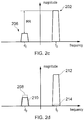
- Figures 2a to 2d illustrate representations of frequency bands that may be obtain by the radio receiver of Figure 1 depending upon its performance characteristics.
- the frequency bands are illustrated in terms of signal magnitude on a vertical axis, against frequency on a horizontal axis.
- the complex digital intermediate frequency signals provided by the front end 100 are such that frequency components do not have any correspondence with opposite, mirror frequency components.
- Figure 2a illustrates an ideal complex IF signal that would be produced by a front end without any IQ amplitude or phase mismatches.
- Such an ideal front end provides a phase difference of exactly 90° ( ⁇ /2) between the in-phase signal and the quadrature signal, and the amplitudes of the in-phase and quadrature signals are exactly the same.
- the ideal output signal of the front end provides a channel 202 at a positive frequency f 0 , and no image 204 of the channel is found at a negative frequency -f 0 .
- Figures 2b and 2c illustrate a non-ideal complex IF signal in which the channel signal 202 is provided at the positive frequency f 0 , and an image 206 of the channel is found at a negative frequency -f 0 .
- an image rejection ratio IRR illustrates the difference between the magnitude of the channel signal 202 and the magnitude of the image 206.
- a result of the IQ mismatch is that if there is a small (wanted) signal 208 to be received at, for example, the negative frequency -f 0 , a strong (blocker) signal 212 that happens to be at the positive frequency +f 0 disturbs or even disables reception of the wanted signal 208.
- the image 210 of the blocker is of a similar magnitude to the small (wanted) signal 208, and so prevents reception at the negative frequency.
- An image 214 is also present at the positive frequency +f 0 due to IQ amplitude and phase mismatches.
- IQ mismatch detection and correction may be employed in the front-end of a radio receiver.
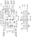
- An implementation of a radio receiver 300 employing a 'one-tap' (single filter notch) IQ correction approach is discussed below with reference to Figures 3a and 3b .
- the receiver 300 has an analogue front end 301 and a digital correction section, which may also be referred to as a compensation system 325.
- the analogue front end 301 has an in-phase path (I path) 302 and a quadrature path (Q path) 304 that are similar to those described previously with reference to Figure 1 .
- I path in-phase path
- Q path quadrature path
- Corresponding series of reference numerals are generally used to describe similar components between the various figures.
- a RF input signal 308 is mixed with intermediate frequency carriers using mixers 306, 316 to generate in-phase (I) and quadrature (Q) components.
- the I and Q components are filtered by filters 310, 318, then amplified by amplifiers 312, 320 and converted to digital signals by analogue-to-digital converters 314, 322.
- the output of the analogue-to-digital converters 314, 322 may contain more than one channel of interest.
- the channels are often located at different frequencies in the signal band that is converted by the converters. Each channel may therefore be considered to be a sub-band of the RF input signal. Further digital processing subsequent to the front end 301 takes care of selecting the wanted channel and suppressing the unwanted channels.
- the compensation system 325 shown in Figure 3a provides a variable gain in the I path 302 to provide relative gain adjustment, as well as an addition of a variable part of the Q path 304 to the I path 302 to provide phase adjustment.
- ADC out A * cos wt + ⁇ + j * A * sin wt
- ADC out A * cos wt * cos ⁇ + sin wt * sin ⁇ + j * A * sin wt
- Cos( ⁇ ) and sin( ⁇ ) are assumed to be constant or very slowly changing, since they represent the phase mismatch of the receiver.
- sin(wt)*sin( ⁇ ) is the error and it can be corrected by subtracting a scaled part the Q path (A*sin(wt)) with coefficient value sin( ⁇ ).
- the amplitude is corrected by the coefficient Amp coef which controls a variable amplifier 328, and the phase is corrected the the coefficient Phase coef which controls the variable amplifier 329.
- An adder 323 adds (or subtracts if the amplification is negative) the amplified Q channel into the I channel.
- the coefficients are derived by a coefficient estimator 327.
- the resulting generated signals I' and Q' have an improved IR performance when the coefficients are set to the correct values. These signals are used by the coefficient estimator, so that a feedback control loop is implemented.
- Figure 3b shows a possible implementation of the coefficient estimator 327.
- the phase coefficient is determined by integrating the correlation between the I' and Q' samples (multiplier 326 for performing the correlation, amplifier 328, integrator 330).
- the amplitude difference is determined by integrating the difference between the absolute sample values of I' and Q' (magnitude units 331, adder 332, amplifier 334, integrator 336).
- phase coefficient and amplitude difference are approximated by the following formulas. For these calculations, symmetrical phase and amplitude errors are applied in the formulas, to simplify the equations.
- IF ADC 1 + ⁇ / 2 * A * cos wt + ⁇ / 2 + j * 1 ⁇ ⁇ / 2 * A * sin wt ⁇ ⁇ / 2
- ⁇ the amplitude difference between the I and Q branch
- ⁇ the phase difference
- A the modulated blocker signal
- w the modulation frequency
- the blocker signal is located at frequency w, and there is an unwanted image at frequency -w.
- the coefficients are obtained by subtracting the absolute values of the I and Q branch for the amplitude estimation, and multiplication of the I and Q branch to obtain the phase information.
- the integrators 330, 336 suppress any high frequency content.
- D 1 + ⁇ / 2 * A * cos wt + ⁇ / 2 ⁇ 1 ⁇ ⁇ / 2 * A * sin wt ⁇ ⁇ / 2
- the average value of the absolute value of a sin or cosine function equals 2/ ⁇ .
- the compensation method usually compensates small amplitude and phase deviation. As such assumption cos( ⁇ /2) ⁇ 1 and sin( ⁇ /2) ⁇ ⁇ /2 can be made to simplify the results.
- Pavg can be estimated by: Pavg ⁇ ⁇ 1 ⁇ 2 * A 2 * ⁇ * 1 ⁇ 1 / 4 ⁇ 2
- Figures 4a and 4b illustrate representations of frequency bands obtained by the front end described with reference to Figures 3a and 3b .
- the form of the representations in Figures 4a and 4b is similar to that described previously with reference to Figure 2 in that signal magnitude is plotted on the vertical axis, against frequency on the horizontal axis.
- Figure 4a illustrates an example in which a relatively narrow bandwidth channel 402 is present at a positive frequency f 0 .
- An image 406 of the channel 402 is present in the output of the analogue front end 301, as described previously with reference to Figure 2b .
- the image signal may be attenuated to provide an attenuated image 407.
- the attenuated image 407 is most reduced in the centre of the bandwidth of the image 406.
- the coefficients are the same as a function of signal frequency, the IR performance is equal for the whole signal band.
- the attenuation of the image obtained by the front end of Figure 3 may therefore be satisfactory for many applications when applied to a narrow bandwidth signal.
- the image rejection (IR) performance of the system described with reference to Figure 3 is optimized for one frequency, and is therefore sub-optimal for the rest of the signal band.
- the receiver may be implemented such that coefficients are optimized for one frequency, while another frequency is of interest. This is a problem for a wide-band system in which multiple frequency sub-bands provide signal content.
- Figure 4b illustrates an example in which a broad bandwidth channel 410 is present at a positive frequency f 0 .
- An image 412 of the channel 410 is present at a corresponding negative frequency -f 0 .
- the IRR peak peak magnitude of the image 412 relative to the magnitude of the channel 410
- the IRR peak is relatively large towards the extremities of the frequency band. Difficulties related to resolving channel interference using the system described with reference to Figure 3 may therefore be encountered in a number of applications despite the good IRR provided at the centre of the frequency band.
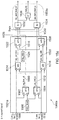
- Figure 5 shows a schematic block diagram of a first example IQ mismatch correction module 500 for providing improved reception of broad bandwidth signals in a radio receiver. That is, for signals with a bandwidth greater than 10 MHz or 25MHz, for example.
- the IQ mismatch correction module 500 comprises an input terminal 502 and an output terminal 504.
- the input terminal 502 is configured to receive an input signal, which may be an intermediate frequency signal.
- the input signal is a time domain signal with a bandwidth.
- the input signal may be provided by a digital domain intermediate frequency signal such as that generated by the front end described previously with reference to Figure 1 .
- the output terminal 504 is configured to provide a corrected output signal from the correction filter.
- the mismatch correction module 500 comprises a mismatch detection module 506 and a filter module 508 provided between the input and output terminals 502, 504.
- the mismatch detection module 506 comprises a bandpass filter unit 510, an amplitude and phase detection unit 512 and a transformation unit 514.
- the bandpass filter unit 510 has a bandpass filter input 520 and a bandpass filter output 522.
- the bandpass filter unit 510 is configured to receive a bandpass input signal at the bandpass filter input 520.
- the bandpass filter unit 510 is configured to select a plurality of n sub-bands by, for each sub-band within the bandwidth, passing the sub-band and blocking, or at least attenuating, other frequencies within the bandwidth that are outside of the sub-band.
- the bandpass filter unit 510 provides bandpass filtered signals for each of the n sub-bands at a bandpass filter output 522.
- the bandpass input signal may be either the input signal from the input terminal 502 or the filtered output signal from the output terminal 504 of the IQ mismatch correction module 500.
- the IQ mismatch correction may be based on a feedforward or feedback signal.
- the input signal may be used as a feedforward signal.
- the bandpass filter signal is the input signal
- the mismatch detection module 506 and the filter module 508 provide separate, parallel signal paths for the input signal within the IQ mismatch correction module 500.
- the amplitude and phase detection unit 512 has an amplitude and phase detection input 524 and an amplitude and phase detection output 526.
- the amplitude and phase detection input 524 is coupled to the bandpass filter output 522.
- the amplitude and phase detection unit 512 is configured to determine amplitude and phase mismatch coefficients [ ⁇ a , ⁇ ⁇ ] n based on the bandpass filtered signals received from the bandpass filter output 522 for the plurality of n sub-bands.
- the amplitude and phase mismatch coefficients [ ⁇ a , ⁇ ⁇ ] n are provided at the amplitude and phase detection output 526.
- the transformation unit 514 has a transformation input 528 and a transformation output 530.
- the transformation input 528 is coupled to the amplitude and phase detection output 526.
- the transformation unit 514 is configured to apply a transformation F([ ⁇ a , ⁇ ⁇ ] n ) to the amplitude and phase mismatch coefficients [ ⁇ a , ⁇ ⁇ ] n to provide filter coefficients for the plurality of n sub-bands at the transformation output 530.
- the transformation F([ ⁇ a , ⁇ ⁇ ] n ) comprise one or more mathematical transformations such as matrix transformations, which could also be an inverse Fourier transformation.
- the transformation unit 514 of the mismatch detection module 506 is configured to generate a set of filter coefficients f 1...n for the plurality of sub-bands, and to provide the generated coefficients f 1...n to the filter module 508 (f 1...n for n/2 bandpass filters, which corresponds to n/2 sub-bands on the positive frequency side and n/2 sub-bands on the negative frequency side).
- the filter module 508 has a signal input 532, a coefficient input 534 and a signal output 536.
- the signal input 532 of the filter module 508 is coupled to the input terminal 502 of the IQ mismatch correction module 500.
- the filter module 508 is configured to filter the input signal from the input terminal 502 in accordance with the filter coefficients [f 1...m ] n received at the coefficient input 534 and to provide the filtered output signal at the signal output 536.
- the signal output 536 is coupled to the output terminal 504 of the IQ mismatch correction module 500.
- the filter 508 may make relatively small amplitude and phase corrections of the order of 1%, and so provides an almost all-pass filter.
- a finite impulse response (FIR) filter may be used to correct frequencies of the input signal in accordance with values of filter coefficients associated with those frequencies in order to provide the output filtered signal.
- the filter module may simultaneously apply the input signal filter coefficients that relate to all of the sub-bands to a single input signal.
- the mismatch detection module 506 may have a sequential processing architecture or a parallel processing architecture.
- a plurality of sub-bands may be obtained by sequentially operating one bandpass filter at different sub-bands or by operating a plurality of bandpass filters in parallel at different sub-bands.
- the bandpass filter unit 510 comprises a plurality of bandpass filters.
- Each of the plurality of bandpass filters is configured to pass a different respective sub-band of the plurality of n sub-bands in order to provide the bandpass filtered signals from the plurality of sub-bands.
- the amplitude and phase detection unit 512 in such examples can comprise a plurality of amplitude and phase mismatch detectors that are configured to receive, in parallel, the respective bandpass filtered signals.
- Each of the amplitude and phase mismatch detectors is configured to determine amplitude and phase mismatch coefficients based on the bandpass filtered signals from a different respective sub-band of the plurality of sub-bands.
- the cut-off frequencies of the passbands and centre frequencies of the parallel bandpass filters may be fixed, or programmable.
- Each of the plurality of bandpass filters (n/2 'double sided', real bandpass filters applied to the complex signal: for n output sub-bands with positive and negative frequencies) may be associated with, and provide a bandpass filtered signal to, one of the plurality of amplitude and phase mismatch detectors.
- the bandpass filter unit 510 may comprise only a single bandpass filter.
- the single bandpass filter is configured to provide the bandpass filtered signals from the plurality of sub-bands by sequentially passing different respective sub-bands of the plurality of sub-bands.
- the sequential operation is not necessarily performed according to a predefined sequence. In the purely sequential case, only one sub-band is analysed by the amplitude and phase detection unit 512 at any one time and so only a single amplitude and phase mismatch detector is required, as described further below with reference to Figure 16 .
- the computational complexity associated with, or hardware footprint e.g.
- bandpass filter unit 510 and the amplitude and phase detection unit 512 are therefore substantially reduced for the sequential processing architecture compared to the parallel processing architecture. Any amount of bandpass filters and amplitude/phase detectors between 1 and number of bands is possible, this depends on the balance power/area and convergence speed required.
- the amplitude and phase mismatch detector 512 in the example of Figure 5 may be implemented, for example, by providing one or more (depending on whether the architecture processes in sequence or parallel) coefficient estimators described with reference to Figure 3b .
- integrators collect amplitude and phase mismatch errors 512 to collect error information and the filter module 508 provides a compensated signal from which the error is deducted (so the filter passes 1 - error).
- the IQ mismatch correction module 500 uses the amplitude and phase mismatch estimates to generate filter coefficients. These coefficients are then implemented by the filter module in a parallel signal path for each of a plurality of sub-bands.
- the IQ mismatch correction module 500 can apply compensation simultaneously in a number of sub-bands, rather than only providing a single filter notch as in the example of Figure 3a .
- signal propagation from the input terminal 502 to the output terminal 504 via the filter module 508 is independent of the signal path from the input terminal 502 or output terminal 504 through the mismatch detection module 506, so the signal transmitted through the filter module 508 is not subject to perturbations introduced by the IQ mismatch correction module 500.
- Figure 6 illustrates a method 600 of correcting an IQ mismatch in an input signal, which may be performed by the module of Figure 5 .
- the method 600 comprises:
- Figure 7 illustrates representations of frequency bands obtained using the module described with reference to Figure 5 or the method described with reference to Figure 6 .
- a broad bandwidth channel 710 is present at a positive frequency f 0 .
- An image 714 of the channel 710 is present at a corresponding negative frequency -f 0 .
- the image of the channel that would be present without compensation is shown as a ghost image 708.
- the compensated image 714 is attenuated with nodes at a plurality of points spaced within the broad bandwidth signal. One node of attenuation is provided for each sub-band of the broad bandwidth signal.
- the magnitude of the image signal is attenuated across the full bandwidth and not only in the centre of the bandwidth.
- the magnitude of the compensated image 714 obtained using the method described with reference to Figure 6 is relatively small towards the extremities of the bandwidth of the signal.
- the interference of the image signal 714 on a desired signal in the same frequency may therefore be reduced compared to the example described previously with reference to Figure 4b .
- the amplitude and phase mismatch detection module may be configured to cyclically generate the amplitude and phase mismatch coefficients by:
- the amplitude and phase mismatch detection module may be further configured to amplify differences prior to integration, as described with reference to Figures 3b and 11a .
- the amplitude and phase mismatch detection module may be configured to decrease a gain of the amplification following initiation of a cycle, as described with reference to Figure 14 . In this way, the settling time of the integration process on an acceptable value may be improved while providing mismatch coefficients with relatively low noise.
- the amplitude and phase mismatch detection module may be further configured to start a new cycle in response to determination of the settled amplitude and phase mismatch coefficients. In this way, the interval of each cycle can be minimized and so the responsiveness of the system can be improved, as described below with reference to Figures 17 and 18 .
- the amplitude and phase mismatch detection module may be configured to use amplitude and phase mismatch coefficients obtained during a previous cycle when determining the amplitude and phase mismatch coefficients for the plurality of sub-bands in a current cycle. In this way, the time taken to generate settled mismatch coefficients may be reduced and so the system responsiveness may be improved.
- the mismatch detection module may be configured to calculate a series of filter coefficients based on the settled mismatch coefficient values from one cycle and the settled mismatch coefficient values from a subsequent cycle in order to avoid sudden substantial changes in the filter coefficients and so avoid distortions in the filter signal. This is described further below with reference to Figures 19 and 20 .
- the mismatch detection module may comprise an interpolation/extrapolation unit as discussed below with reference to Figures 9 , 22 and 23 .
- the interpolation/extrapolation unit may be configured to receive the amplitude and phase mismatch coefficients and to determine further amplitude and phase mismatch coefficients by interpolating and/or extrapolating values based on the received amplitude and phase mismatch coefficients. In this way, the noise level in the filter coefficients may be reduced.
- the mismatch detection module may comprise level detection circuitry as discussed below with reference to Figures 15a , 15b .
- the level detection circuitry may be configured to identify positive or negative frequencies associated with sub-bands that contain useful information.
- the mismatch detection module may generate filter coefficients based on the identified positive or negative frequencies as discussed with reference to Figures 11a and 12 . In this way, the noise level in the filter coefficients may also be reduced.
- Figures 8 and 9 illustrate second and third example IQ mismatch correction modules 800, 900 with parallel processing architecture for processing a plurality of n sub-bands of a broad bandwidth signal. Bandpass filtering and amplitude and phase mismatch detection is performed separately for each sub-band in the parallel processing architecture by respective signal paths 818a-n, 918a-n. Each signal path illustrated in Figures 8 and 9 relates to separate I and Q parts of a signal.
- Both the second and third example IQ mismatch correction modules 800, 900 each comprise a filter module 808, 908 that is similar to that described previously with reference to Figure 5 .
- the bandpass filters 810a-n, 910a-n of the IQ mismatch correction modules 800, 900 in these examples comprise level estimators.
- Level estimation provides an indication of whether a positive or negative frequency in the sub-band includes useful signal information. The calculation of level estimates is discussed further with reference to the example level selectors of Figures 15a and 15b .
- each signal path 818a-n provides a bandpass filter 810a-n and an amplitude and phase error detector 812a-n.
- the functionality of the bandpass filters 810a-n and amplitude and phase mismatch detectors 812a-n is similar to that described previously with reference to Figure 5 .
- Each bandpass filter 810a-n has a bandpass filter input 820a-n and a bandpass filter output 822a-n.
- the bandpass filters 810 are each coupled to a switch 838 that connects the bandpass filter inputs 820a-n to either the input terminal 802 or the output terminal 804 of the IQ mismatch correction module 800.
- Each amplitude and phase mismatch detector 812a-n has an amplitude and phase detection input 824a-n and an amplitude and phase detection output 826a-n.
- the amplitude and phase detection input 824 of a particular amplitude and phase mismatch detector 812a-n is coupled to the bandpass filter output 822a-n of a bandpass filter 810an that is associated with the same signal path 818a-n as that particular amplitude and phase mismatch detector 812a-n.
- the transformation module comprises a polar-to-Cartesian transformation block 840a-n for each signal path 818a-n, and a filter coefficient calculator 846.
- Each polar-to-Cartesian transformation block 840a-n has a Cartesian transformation input 842a-n and a Cartesian transformation output 844a-n.
- the Cartesian transformation input 842a-n of a particular polar-to-Cartesian transformation block 840a-n is coupled to the amplitude and phase detection output 826a-n of an amplitude and phase mismatch detector 812a-n associated with the same signal path 818a-n as that particular polar-to-Cartesian transformation block 840a-n.
- the role of the polar-to-Cartesian transformation block 840a-n is to convert the phase and amplitude mismatch coefficients calculated by the phase and amplitude mismatch detectors 812a-n, which may be represented by polar coordinates, to real and imaginary frequency components that may be represented by Cartesian coordinates and are suitable for use as inputs to a matrix transform.
- the real and imaginary frequency components may therefore be considered as transformed amplitude and phase mismatch coefficients.
- the polar to Cartesian transformation may be performed periodically, rather than in real time, in order to reduce computational requirements in the system. The period computations are not necessarily over a regular or fixed period. The interval between calculation of the polar to Cartesian transformation affects the responsiveness of the system and so may be selected in accordance with expected signal mismatch evolution.
- Each Cartesian transformation output 844a-n is provided as an input of the filter coefficient calculator 846.
- the filter coefficient calculator 846 may be implemented by a matrix transform, as discussed in further detail below with reference to Figure 24 .
- the transformation may comprise an inverse fast Fourier transformation.
- the transformation of the filter coefficient calculator 846 acts on the transformed amplitude and phase mismatch coefficients and provides correction filter coefficients.
- the filter coefficient calculator 846 provides the filter coefficients at a transformation output 830.
- the third example IQ mismatch correction module 900 is generally similar to that described previously with reference to Figure 8 but further comprises a plurality of n automatic gain controllers 916a-n and an interpolation/extrapolation unit 948.
- One automatic gain controller (AGC) 916a-n is provided for each of the plurality of n sub-bands in the respective signal paths 918a-n.
- the automatic gain controllers 916a-n each have an AGC input 950a-n and an AGC output 952a-n.
- the AGC input 950a-n of a particular AGC 916a-n is coupled to a bandpass filter output 922 of a bandpass filter 910a-n that is associated with the same signal path 918a-n as that particular AGC 916a-n.
- the automatic gain controllers 916a-n each receive a bandpass filtered signal from a bandpass filter 910a-n associated with the same signal path 918a-n as that automatic gain controller 916a-n and perform gain control on the bandpass filtered signal.
- the AGC output 952a-n of a particular AGC 916a-n is coupled to the amplitude and phase mismatch detector input 942a-n of the amplitude and phase mismatch detector 912a-n that is associated with the same signal path 918a-n as that particular AGC 916an.
- the bandpass filtered signal is therefore provided by each AGC 916a-n to an amplitude and phase mismatch detector 912a-n associated with that respective automatic gain controller 916a-n. It has been found that use of AGCs results in a faster convergence time for low amplitude sub-band signals, as discussed further below with reference to Figures 13a , 13b and 14 .
- All of the amplitude and phase detection outputs 926a-n are connected to the interpolation/extrapolation unit 948 in order to provide the amplitude and phase mismatch coefficients to the interpolation/extrapolation unit 948.
- the interpolation/extrapolation unit 948 is configured to determine further amplitude and phase mismatch coefficients for sub-bands within the broad bandwidth by interpolating and/or extrapolating values based on the received amplitude and phase mismatch coefficients. Possible implementations of the interpolation/extrapolation unit 948 are discussed further below with reference to Figures 22 and 23 .
- the amplitude and phase mismatch coefficients are provided by the interpolation/extrapolation unit 948 to the transformation module 914.
- the implementation of the transformation module 914 is similar to the example described previously with reference to Figure 8 .
- the arrows representing dataflow to, from and within the transformation module 914 in Figure 9 represent the parallel flow of data the separate signal path associated with the respective sub-bands.
- the automatic gain controllers 916a-n and the interpolation/extrapolation unit 948 may be provided independently of one another in other examples.
- similar automatic gain controllers and/or interpolators may also be used in the first example described previously with reference to Figure 5 .
- Figures 10a to 10f illustrate signals associated with an implementation of the IQ mismatch correction module described previously with respect to Figures 5 , 8 and 9 .
- Figure 10a illustrates example profiles prior to amplitude and phase mismatch correction of phase mismatch 1002 in rad and amplitude mismatch 1004 in fullscale ratio against frequency (in Hz) for an IQ mismatch in an intermediate frequency signal introduced by the analogue reception path.
- the phase mismatch here is roughly linear and has a zero crossing at about -5 MHz. The biggest amplitude mismatch occurs at about 0 Hz, and is smaller at both positive and negative frequencies.
- Arrows show mid frequency positions 1006, 1008, 1010 of first, second and third bandpass filters (filter1, filter2, filer3) operating on three of a plurality of sub-bands.
- Figure 10b illustrates the convergence of the phase and amplitude detector for the first filter (filter1) discussed above with reference to Figure 10a .
- the detected amplitude error 1016 converges to the amplitude error at the mid frequency of the first filter (filter1), as depicted for curve 1004 in figure 10a .
- the detected phase error 1014 converges to the phase error at the mid frequency of the first filter (filter1), as depicted for curve 1002 in figure 10a .
- Figure 10c illustrates the convergence of the phase- and amplitude detector for the second filter (filter2) discussed above with reference to Figure 10a .
- the detected amplitude error 1020 converges to the amplitude error at the mid frequency of the second filter (filter2), as depicted for curve 1004 in figure 10a .
- the detected phase error 1018 converges to the phase error at the mid frequency of the second filter (filter2), as depicted for curve 1002 in figure 10a .
- Figure 10d illustrates the convergence of the phase- and amplitude detector for the third filter (filter3) discussed above with reference to Figure 10a .
- the detected amplitude error 1024 converges to the amplitude error at the mid frequency of the third filter (filter3), as depicted for curve 1004 in figure 10a .
- the detected phase error 1022 converges to the phase error at the mid frequency of the third filter (filter3), as depicted for curve 1002 in figure 10a .
- Figure 10e illustrates the peak image rejection ratio (IRR) in dB against time (in ms) of filtered signals at the output of the IQ mismatch detector.
- the settling time of the system is about 10 ms. During this time, integrators within the amplitude and phase mismatch detectors are converging on a value.
- Figure 10f illustrates the magnitude of various signals against frequency.
- the signals represent a broad bandwidth channel 1032, with a bandwidth of about 10 MHz centred at a negative frequency, and an image 1034 centred at a corresponding positive frequency. Three representations of the image 1034 are shown.
- An uncompensated image 1036 has a high magnitude throughout its bandwidth, as discussed above with reference to Figures 4b and 7 .
- a 'single tap' compensated image 1038 such as that provided by the compensation system described with reference to Figures 3a and 3b , attenuates the image at a node adjacent to the centre of the frequency band, as discussed previously with reference to Figure 4b .
- a 'multi-tap' compensated image 1040 such as that provided by the IQ mismatch correction module described with reference to Figures 5 , 8 or 9 , attenuates the image at a plurality of nodes throughout the frequency band, as discussed previously with reference to Figure 7 .
- Figure 11a illustrates an example amplitude and phase mismatch detector 1112i for use in the IQ mismatch correction module described previously with reference to Figures 5 , 8 and 9 .
- the amplitude and phase mismatch detector 1112i is based on the coefficient estimator described previously with respect to Figure 3b .
- each phase coefficient is determined by integrating a correlation between in-phase and quadrature samples for both the positive and negative frequencies of the sub-band and the desired polarity of frequency is selected for use.
- the amplitude and phase mismatch detector 1112i comprises an in-phase input 1174 and a quadrature input 1176.
- the quadrature and phase input signals are corrected by the current found correction values, in a similar way as for the single tap case like described in figure 3a and 3b .
- the correction signal is selected with multiplexers 1140, 1142.
- the amplitude and phase mismatch detector 1112i can choose to not compensate when no proper signal is present, as determined by signal level selection circuitry discussed below with reference to Figure 15a , or to select the coefficient for the positive band when a 'proper blocker' is present in the positive band, or the coefficient for the negative band when a 'proper blocker' is present in the negative band.
- the amplitude and phase mismatch detector 1112i comprises an in-phase variable gain amplifier 1180 and a quadrature variable gain amplifier 1182.
- the in-phase variable gain amplifier 1180 receives an in-phase input signal from the in-phase input 1174.
- the quadrature variable gain amplifier 1182 receives a quadrature input signal from the quadrature input 1176.
- a first adder 1184 adds signals from the in-phase variable gain amplifier 1180 and the quadrature variable gain amplifier 1182 to provide a compensated in-phase signal.
- the first magnitude determining unit 1131a receives the quadrature input signal from the quadrature input 1176.
- a second magnitude determining unit 1131b receives the compensated in-phase signal from the first adder 1184.
- a second adder 1132 has an addition input connected to an output of the second magnitude determining unit 1131b and a subtraction input connected to an output of the first magnitude determining unit 1131a. The result of the addition performed by the second adder 1132 is provided to a positive band amplitude integrator 1136a and to a negative band amplitude integrator 1136b via respective amplifiers 1134a, 1134b.
- a multiplier 1126 is configured to multiply the in-phase signal from the compensated in-phase signal from the first adder 1184 and the quadrature signal from the quadrature input 1176 to provide a multiplied signal.
- the multiplied signal is provided to a positive phase integrator 1136c and to a negative phase integrator 1136d via respective amplifiers 1134c, 1134d.
- Each of the integrators 1136a-d has an enabling input.
- the positive phase integrator 1136c and the positive amplitude integrator 1136a have a common enabling input.
- the negative phase integrator 1136d and the negative amplitude integrator 1136b also have a common enabling input.
- the amplitude and phase mismatch detector 1112i may be enabled to provide amplitude and phase mismatch coefficients related to either a positive or negative frequency of the sub-band. Operation of the amplitude and phase mismatch detector 1112i is discussed below with reference to Figures 11b and 11c .
- a first multiplexor 1140 has a first selectable input, a second selectable input, a third selectable input, a first multiplexor input, a second multiplex input and an output.
- the first selectable input of the first multiplexor 1140 is connected to the output of the positive amplitude integrator 1136a.
- the second selectable input of the first multiplexor 1140 is connected to the negative amplitude integrator 1136b.
- the third selectable input of the first multiplexor 1140 receives a null input.
- the first multiplexor input of the first multiplexor 1140 provides a common enabling input with the positive phase integrator 1136c and the positive amplitude integrator 1136a.
- the second multiplexor 1140 of the first multiplexor 1140 provides a common enabling input with the negative phase integrator 1136d and the negative amplitude integrator 1136b.
- the output of the first multiplexor 1140 and a unity input are added together by a third adder 1186 and the output of the third adder eliminated 6 controls the in-phase variable gain amplifier 1180.
- a second multiplexor 1142 has a first selectable input, a second selectable input, a third selectable input, a first multiplexor input, a second multiplex input and an output.
- the first selectable input of the second multiplexor 1142 is connected to the output of the positive phase integrator 1136c.
- the second selectable input of the second multiplexor 1142 is connected to the negative phase integrator 1136d.
- the third selectable input of the second multiplexor 1142 receives a null input.
- the first multiplexor input of the second multiplexor 1142 provides a common enabling input with the positive phase integrator 1136c and the positive amplitude integrator 1136a.
- the second multiplexor 1140 of the second multiplexor 1142 provides a common enabling input with the negative phase integrator 1136d and the negative amplitude integrator 1136b.
- the output of the second multiplexor 1142 controls the quadrature phase variable gain amplifier 1182.
- Figure 11b illustrates an example zero-IF signal.
- the zero-IF signal contains four sub-bands containing sets of positive and negative frequencies at either a low magnitude 1154 or a high magnitude 1156.
- a first sub-band contains a first high magnitude signal 1158 at a first positive frequency +f 1 and a first low magnitude signal 1160 at a first negative frequency -f 1 .
- a second sub-band contains a second high magnitude signal 1162 at a second negative frequency -f 2 and a second low magnitude signal 1164 at a second positive frequency +f 2 .
- a third sub-band contains a third high magnitude signal 1166 at a third positive frequency +f 3 and a third low magnitude signal 1168 at a third negative frequency -f 3 .
- a fourth sub-band contains a fourth high magnitude signal 1170 at a fourth negative frequency -f 4 and a fourth low magnitude signal 1172 at a fourth positive frequency +f 4 .
- FIG 11c illustrates four signal paths 1118a-d of a mismatch detector module.
- Each signal path 1118a-d comprises a bandpass filter 1110a-d and an amplitude and phase mismatch detector 1112a-d such as that described previously with reference to Figure 11a .
- Each bandpass filter 1110a-d is configured to select one of the sub-bands discussed previously with respect to Figure 11b .
- Representations of the selected frequencies are also illustrated next to the bandpass filters 1110a-d in Figure 11c .
- the dotted lines on the representations of the selected frequencies illustrate the shaping profiles of the bandpass filters 1110a-d. Circuitry for selecting whether to select the negative frequency of the positive frequency is described above with reference to Figure 11a and further below with reference to Figure 15 .
- Figure 12 illustrates another example signal path 1218 for operating on a sub-band in a mismatch detection module.
- the signal path 1218 comprises a bandpass filter and level estimation unit 1210, an automatic gain controller (AGC) 1216 and an amplitude and phase mismatch detector 1212.
- the bandpass filter and level estimation unit 1210 has a bandpass input 1220 and the bandpass output 1222.
- the bandpass input 1220 is configured to receive a bandpass input signal as described previously with reference to Figure 5 , for example.
- the AGC 1216 has an AGC input 1250 and an AGC output 1252.
- the AGC input 1250 is connected to the bandpass output 1222.
- the amplitude and phase mismatch detector 1212 has a first input 1290 connected to the bandpass output 1222 and a second input 1292 connected to the AGC output 1252.
- the amplitude and phase mismatch detector 1212 also has a disable input 1294.
- a controller 1296 comprising a five input OR gate disables the amplitude and phase mismatch detector 1212 in response to the following conditions:
- Figures 13a and 13b illustrate coefficient profiles of amplitude and phase mismatch coefficients obtained as a function of time after initiation of integrators in an amplitude and phase mismatch detection module, such as those described previously with reference to Figures 3b and 11a .
- the amplifiers in the amplitude and phase mismatch detection module provide a gain, which may also be referred to as loop gain.
- Figure 13a shows an amplitude coefficient profile 1302 and a phase coefficient profile 1304 for a system with 'low' loop gain (of the order of 1 x 10 -4 ).
- Figure 13b shows an amplitude coefficient profile 1306 and a phase coefficient profile 1308 for a system with 'high' loop gain (of the order of 1 x 10 -3 ).
- the convergence speed of the IQ mismatch correction module may be determined by considering the period in which it takes the coefficients 1302, 1304, 1306, 1308 to settle on a stable value.
- the conversion speed for the IQ mismatch correction module with low loop gain is unacceptably slow for many applications because the amplitude coefficient profile 1302 and phase coefficient profile 1304 settle on a stable value after about 60 ms, resulting in poor responsiveness of the system as a whole.
- the conversion speed for the IQ mismatch correction module with high loop gain is acceptable for most applications because the amplitude coefficient profile 1306 and phase coefficient profile 1308 settle on a stable value after about 0.1 ms.
- Figure 14 illustrates an amplitude coefficient profile 1410 and a phase coefficient profile 1412 obtained as a function of time after initiation of integration in an IQ mismatch correction module with variable loopgain 1414.
- the loopgain 1414 is also plotted as a function of time with the amplitude and phase coefficient profiles 1410, 1412.
- the loop gain linearly decreases from a 'high' loop gain of about 1 x 10 -3 to a 'fow' loop gain of about 1 x 10 4 between 0 and 0.4 ms.
- the loop gain By decreasing the loop gain as a function of time following the initiation of integration, the benefits of both low and high loop gain can be obtained.
- the coefficient value At the start of the period when the loop gain is high, the coefficient value rapidly converges, albeit with high noise. Later in the period when the loop gain is reduced, the coefficient values are already near or at a settled value and the reduction in loop gain reduces the noise in the coefficient value.
- the scheme therefore provides a balance between conversion speed and accuracy that are suitable
- variable loop gain within the correction module in Figure 3b still results in a 'noisy' signal for the first part of the convergence-time, which leads to contamination of the compensated output signal because the determined mismatch correction is applied directly to the input signal to provide the compensated output signal.
- the compensating filter is decoupled from the mismatch detection module in that they act on parallel signal paths.
- the mismatch detection module may therefore work on the bandpass filter input signal without directly changing the radio-frequency input signal that is provided at the output. This leaves the signal chain clean and free from coefficient convergence noise.
- the filter module may therefore be configured to only apply filtering when suitably converged mismatch coefficient values are found (using a low loopgain, for example). At that point, the matrix transformation is executed and the compensation filter coefficients are updated. In this way, initially between start up and a first correction coefficient update, there may be no IQ correction applied to the IQC input signal. As such, the IQ-matching may be limited to 'analog IQ matching' until the filter gets a coefficient update. This would lead to an IRR of roughly 50dB in the example discussed above with regard to Figure 10f , but waiting for this 'offline' coefficient searching enables fast coefficient tracking without contaminating the main signal with noise, as shown with figures 13 , 14 .
- Another approach for reducing conversion time is, on initiation of integration within the amplitude and phase mismatch detector for a particular sub-band, to load mismatch coefficient values that were found in a previous active calibration state for that sub-band.
- the settling time may be reduced because the previously found values are more likely to be roughly correct.
- a controller may be provided in a mismatch detection module in order to decrease the loop gain in the mismatch detection module following initiation of determination of the amplitude and phase mismatch coefficients, and so reduce conversion time.
- the controller may also be configured to use previously determined amplitude and phase mismatch coefficients, or related values, when determining the present amplitude and phase mismatch coefficients for the plurality of sub-bands.
- Figure 15a illustrates a level selection circuit 1500a for determining whether to select a positive or negative frequency of sub-band of an intermediate frequency signal.
- Level selection enables the mismatch detection unit to use only positive or negative frequency components of sub-bands that include useful signal information.
- the level selection circuit 1500a comprises a main path 1501a and logic circuitry 1503a.
- the level selection circuit 1500a is configured to receive a negative frequency signal level 1506 and a positive frequency signal level 1510 which may be generated, for example, by averaging the rectified bandpass filtered signals for the respective positive and negative frequencies of the sub-band.
- a first order low pass filter may be used to average the rectified bandpass filtered signals.
- the main path 1501a comprises a first comparison unit 1502 and a second comparison unit 1504.
- the first comparison unit 1502 compares a negative frequency signal level 1506 of a current sub-band with a minimum level 1508 and provides the comparison output (digital one or zero)1509.
- the second comparison unit 1504 compares a positive frequency signal level 1510 and provides the comparison output (digital one or zero)1512.
- the main path 1501a also comprises a first divider 1514 and a second divider 1518.
- the first divider 1514 is configured to divide the negative frequency signal level 1506 by the positive frequency signal level 1510 to provide a negative to positive ratio 1516.
- the second divider 1518 is configured to divide the positive frequency signal level 1510 by the negative frequency signal level 1506 to provide a positive to negative ratio 1520.
- the main path 1501 a also comprises a third comparison unit 1522 and a fourth comparison unit 1528.
- the third comparison unit 1522 is configured to compare the negative to positive ratio 1516 with a minimum ratio 1524 and to provide the third comparison output (digital one or zero) 1526.
- the fourth comparison unit 1528 is configured to compare the positive to negative ratio 1520 with the minimum ratio 1524 and to provide the comparison output (digital one or zero) 1530.
- the logic circuitry 1503a comprises first and second three-input AND gates 1532, 1534 and an OR gate 1536 that is configured to receive output signals from the first and second 3 input AND gates 1532, 1534 and to provide an indication of a valid signal.
- the first three-input AND gate 1532 receives:
- the second three-input AND gate 1534 receives:
- the level detectors supply the IQ error detectors with information on proper signal conditions in the different bands. If the level detection is slow, with large time constants, the detected level is quite stable, but because of the latency, information for fast changing signals constellations could be too old, could lead the IQ error detectors summing up IQ error information for the wrong band or detect inappropriate signals.
- FIG. 15b illustrates a further level selection circuit 1500b.
- the level selection circuit 1500b comprises a second, slow path 1501c in addition to a first, fast path 1501b.
- the slow and fast detection paths 1501b, 1501c are similar to the main path 1501a described previously with reference to Figure 15a , but receive negative and positive frequency signal levels that have been averaged over different time periods.
- the fast negative and positive frequency signal levels have been averaged over a shorter time period than the slow negative and positive frequency signal levels.
- the fast negative and positive frequency signal levels are therefore affected by short bursts or pulses that are effectively filtered from the slow negative and positive frequency signal levels.
- the slow negative and positive frequency signal levels suffer from a delay due to averaging.
- a combination of slow and fast level detection leads to improved level indication signal for IQC error detection.
- the level selection circuit 1500b in Figure 15b comprises logic circuitry 1503b that differs from the logic circuitry 1503a described above with reference to Figure 15a in that the first and second three-input AND gates are replaced by corresponding first and second five-input AND gates 1532b, 1534b.
- the additional terminals of the five-input AND gates 1532b, 1534b are connected to third and fourth comparison outputs 1526c, 1530c of the third and fourth comparators 1522c, 1528c of the second, slow path, 1501c.
- the level selection circuit 1500b supplies the mismatch detectors with information on proper signal conditions in the different bands. If the level detection is slow, with large time constants, the detected level is quite stable, but because of the latency, information for fast changing signals constellations could be too old, could lead the IQ error detectors summing up IQ error information for the wrong band or detect inappropriate signals.
- Figure 16 illustrates a time slicing profile for an IQ mismatch correction module with a sequential processing architecture.
- the sequential processing architecture may be implemented using time division multiplexing in which the bandpass filter input signal is divided into a plurality of up to n slices 1600a-n, which may have different sizes. Each slice 1600a-n is provided to the bandpass filter and to the phase and amplitude mismatch detector in real-time.
- a controller is provided in such an IQ mismatch correction module in order to set the bandpass filter to filter a different sub-band of the bandpass filter input signal for each of the n slices in order that the bandpass filter and phase and amplitude mismatch detector together provide phase and amplitude mismatch coefficients for each of a plurality of n sub-bands.
- Figure 17 illustrates a portion of a controller 1700 for determining when to set a bandpass filter of a mismatch detection module to pass a different sub-band to a current sub-band.
- the portion of a controller 1700 is configured to provide a change sub-band signal in response to the phase mismatch coefficient changing less than a predetermined phase mismatch change value in a predetermined time period and the amplitude mismatch coefficient changing less than a predetermined amplitude mismatch change value in the predetermined time period.
- the portion of the controller 1700 comprises an amplitude difference determining unit 1702, a phase difference determining unit 1704, counting circuitry 1706 and logic circuitry 1708.
- the amplitude difference determining unit 1702 comprises a first register 1708 and a second register 1710. Each register has a data input D, a reset terminal R and an output Q.
- An amplitude maximum signal block 1712 provides the greater of a signal at the output Q of the first register 1708 and the amplitude coefficient from the phase and amplitude mismatch detector to the data input D of the first register 1708.
- An amplitude minimum signal block 1714 provides the lesser of a signal at the output Q of the second register 1710 and the amplitude coefficient from the phase and amplitude mismatch detected to the data input D of the second register 1710.
- a first adder 1716 receives the signal at the output Q of the first register 1708 at an addition input and the output Q of the second register 1710 at a subtraction input.
- a first comparator 1718 receives the result determined by the first adder 1716 at an inverting input. The first comparator 1718 receives an amplitude threshold indicative of a predetermined amplitude mismatch change at a noninvert
- the phase difference determining unit 1704 comprises a third register 1720 and a fourth register 1722. Each register has a data input D, reset terminal R and an output Q.
- a phase maximum signal block 1724 provides the greater of a signal at the output Q of the third register 1720 and the phase coefficient from the amplitude and phase mismatch detector to the data input D of the third register 1720.
- a phase minimum signal block 1726 provides the lesser of a signal at the output Q of the fourth register 1722 and the phase coefficient from the amplitude and phase mismatch detected to the data input D of the fourth register 1722.
- a second adder 1728 receives the signal at the output Q of the third register 1720 at an addition input and the output Q of the fourth register 1722 at a subtraction input.
- a second comparator 1730 receives the result determined by the second adder 1728 at an inverting input. The second comparator 1730 receives a phase threshold indicative of a predetermined phase mismatch change at a noninverting input.
- the counting circuitry 1706 comprises a counter configured to count up to a window size, N. Once the counter reaches the window size N it provides a signal at a counter output and resets itself. The signal at the counter output resets the registers 1708, 1710, 1720, 1722 of the amplitude and phase difference determining units 1702, 1704
- the logic circuitry comprises the equivalent of a three-input AND gate that receives inputs from the output of the counting circuitry 1706, the first comparator 1718 of the amplitude difference determining unit 1702 and the second comparator 1730 of the phase difference determining unit 1704.
- Figure 18 illustrates an amplitude mismatch coefficient 1802 generated by an amplitude mismatch detector as a function of time.
- An amplitude threshold 1804 for use in the controller of Figure 17 is also illustrated in Figure 18 .
- the amplitude threshold 1804 is indicative of a predetermined amplitude mismatch change below which the amplitude mismatch coefficient is considered to have settled on a value.
- the controller of Figure 17 progresses through a number of counter cycles 1806 before the amplitude mismatch coefficient 1802 settles within the amplitude threshold 1804.
- the controller were to set the bandpass filter of the mismatch detection module to filter the next sub-band at the end of the fourth counter cycle 1808, which is the first cycle in which the amplitude mismatch coefficient 1802 is within the amplitude threshold 1804, rather than at a predetermined fixed period 1810, then the iteration time of the IQ mismatch correction module is reduced, and so for a sequentially implemented architecture the module may be more responsive to fast changing signals.
- the separation of the mismatch detection module from the correction filter module means that the coefficients of the filter module are updated periodically, or intermittently, and so errors introduced during the settling time of the mismatch detection module do not affect the filter and perform other filter module.
- filter coefficient interpolation may be performed.
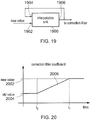
- Figure 19 illustrates a filter coefficient smooth update interpolation unit 1900. This block is not to be confused with interpolation performed by the interpolation/extrapolation unit of the mismatch detection module described previously with reference to Figure 9 , and described further below with reference to Figures 22 and 23 or with the correction filter interpolation matrix.
- the filter coefficient smooth update interpolation unit 1900 has a first input 1902, second input 1904 and an output 1906.
- the first input 1902 is configured to receive new values of the filter coefficients from the transformation module described previously with reference to Figures 5 , 8 and 9 .
- the output 1906 is configured to provide filter coefficients to the filter module described previously with reference to Figures 5 , 8 and 9 .
- the second input 1904 also receives the filter coefficients from the output 1906 in a feedback loop.
- Figure 20 illustrates signals associated with the filter coefficient interpolation unit of Figure 19 for a particular filter coefficient.
- the filter coefficient has a new value 2002 and an old value 2004.
- the new value 2002 is different from the old value 2004.
- the filter coefficient interpolation unit performs linear interpolation between the old value 2004 and the new value 2002.
- the resultant filter coefficient 2006 at the output of the filter coefficient interpolation module increases linearly between the new and old values 2002, 2004 as a function of time.
- Other interpolation functions such as a cosine, may be used instead of a linear function.
- the application of interpolation may reduce the disturbance that would be induced by applying a step change in the filter coefficients directly at the filter module at a calculation time to of the new value 2002. Instead, the new value 2002 is applied at a later time t 1 following a ramping period between the old value 2004 and the new value 2002.
- the interpolation/extrapolation unit of the mismatch detection module described previously with reference to Figure 9 may be configured to select and discard sub-bands in order to provide interpolated or extrapolated coefficients as improved estimates of IQ errors in sub-bands, which do not yet contribute with reasonable signals (e.g. according to figure 15 ).
- Figure 21 illustrates a profile 2100 of filtered signal magnitude against frequency for a broad bandwidth signal comprising four sub-bands, each sub-band having a positive frequency and a negative frequency.
- a first sub-band comprises a first positive frequency signal +f 1 with a substantially higher magnitude than a corresponding negative frequency signal -f 1 .
- a second sub-band comprises a second positive frequency signal +f 2 with a magnitude that is similar to that of a corresponding second negative frequency signal -f 2 .
- a third sub-band comprises a third negative frequency signal -f 3 that is substantially higher than a corresponding third positive frequency signal +f 3 .
- a fourth sub-band comprises fourth positive and negative frequency signals +f 4 ,-f 4 with a low magnitude.
- a mismatch detection module may be configured to base interpolated or extrapolated values on coefficients of positive frequency components in sub-bands in which the negative frequency components are relatively low, or vice versa.
- the mismatch detection module may also be configured to discard the coefficients from sub-bands in which the positive and negative frequency components are of a similar amplitude, or both of a low amplitude.
- Two amplitudes or magnitudes may be considered to be similar to each other when they differ by less than the threshold level.
- An amplitude or magnitude may be considered to be low if it is equal to or less than the threshold level.
- Figure 22 illustrates a profile 2200 of the amplitude mismatch coefficients, determined by an amplitude and phase mismatch detector as previously discussed with reference to Figure 21 , against frequency for a broad bandwidth signal comprising four sub-bands. Each sub-band has a positive frequency and a negative frequency.
- the profile 2200 comprises detected amplitude mismatch coefficients 2202 at a first positive frequency +f 1 and a third negative frequency -f 3 .
- Missing (or discarded) frequencies 2204 within the bandwidth at second, third and fourth positive frequencies f 2 , f 3 , f 4 and first, second and fourth negative frequencies -f 1 , -f 2 , -f 4 can be calculated by applying a curve fit interpolation using an interpolation/extrapolation unit of the mismatch detection module.
- the interpolation/extrapolation unit provides interpolated mismatch coefficients at the second, third and fourth positive frequencies f 2 , f 3 , f 4 and the first, second and fourth negative frequencies -f 1 , -f 2 , -f 4 .
- the interpolation or extrapolation function applied by the interpolation/extrapolation unit may be zero order or first order to reduce computational requirements.
- Figure 23 illustrates a profile of amplitude mismatch coefficients plotted against frequency for a broad bandwidth signal comprising four frequency bands according to figure 21 .
- the profile 2300 comprises detected amplitude mismatch coefficients 2302 at a first positive frequency +f 1 and a third negative frequency -f 3 .
- interpolated mismatch coefficients at third positive frequencies f 3 and first negative frequencies -f 1 are calculated by an interpolation/extrapolation unit substituting missing (or discarded) positive coefficient values 2304 with the corresponding detected negative coefficient values, and vice versa. The effect of the substitution is that the coefficient values are mirrored about the vertical axis.
- the remaining missing mismatch coefficients at second and fourth positive frequencies f 2 , f 4 and second and fourth negative frequencies -f 2 , -f 4 may be interpolated as described for figure 22 .
- Figure 24 illustrates an IQC bandpass filter bank profile 2400.
- the filter bank profile comprises filters for defining a plurality of sub-bands with positive and negative frequencies, including a first sub-band 2402a, 2402b, a second sub-band 2404a, 2404b, a third sub-band 2406a, 2406b and a fourth sub-band 2408a, 2408b.
- the plurality of sub-bands have arbitrary mid frequencies and bandwidths. As such, implementations of the band-pass filters described herein need not have equidistant frequency midpoints and so may afford a high degree of flexibility to the receiver design.
- the first sub-band 2402a, 2402b and fourth sub-band 2408a, 2408b have broader bandwidths than the second sub-band 2404a, 2404b and third sub-band 2406a, 2406b.
- the application of an IDFT is not suitable here, because the IDFT requires equidistant frequency points, which is not given here.
- the construction of the filter coefficients from determined mismatch coefficients requires generation of an FIR filter that has the given transfer at the given frequency positions given a number of transfer coefficients at arbitrary, given frequency positions.
- the mismatch coefficients are assumed to be complex values, and the FIR filter may be likewise a complex filter.
- the transfer coefficients are given at frequency positions, that is, they are given on the unit circle in the z domain.
- the frequency response of the target FIR filter is periodic when viewed as a function of the position on the unit circle.
- the second part of the problem is greatly reduced by choosing a suitable form of interpolation.
- periodic functions may be used as a basis for the interpolation.
- the basis used for interpolation is the doubly infinite sequence: ... e ⁇ 4 ⁇ if / f 0 e ⁇ 2 ⁇ if / f 0 1 e 2 ⁇ if / f 0 e 4 ⁇ if / f 0 ... , where f 0 is the sample rate used.
- the interpolation is done with the Fourier basis of functions, and expressing the interpolation function with respect to this basis is merely a Fourier transform.
- the filter coefficients are equal to the impulse (any filter in the discrete time domain has a periodic transfer) response, which is in turn equal to the Fourier transform of its transfer function.
- the Fourier transform that is necessary to obtain the filter coefficients is automatically executed, and the FIR filter coefficients are simply the main result of the interpolation itself.
- the second part of the problem may be solved by taking the interpolation coefficients, and using them straightforwardly as FIR filter coefficients.
- the complex numbers c k are the interpolation coefficients to be found.
- the inverse matrix A - 1 can be calculated off-line. In that case, the only calculation to be executed by the system is a standard matrix multiplication.
- the matrix multiplication executes a transform between function bases, which effectively combines the operations of interpolation and Fourier transform.
- One freedom of design is the sample rate. If the sample rate is too tight, the transfer function has a steep part around ⁇ 1 ⁇ 2 f 0 , leading to oscillations in the interpolated transfer function similar to the Gibbs phenomenon. In such cases, it may be helpful to increase the sample rate, so as to reduce the steepness around ⁇ 1 ⁇ 2 f 0 .
- the set of instructions/method steps described above are implemented as functional and software instructions embodied as a set of executable instructions which are effected on a computer or machine which is programmed with and controlled by said executable instructions. Such instructions are loaded for execution on a processor (such as one or more CPUs).
- processor includes microprocessors, microcontrollers, processor modules or subsystems (including one or more microprocessors or microcontrollers), or other control or computing devices.
- a processor can refer to a single component or to plural components.
- the set of instructions/methods illustrated herein and data and instructions associated therewith are stored in respective storage devices, which are implemented as one or more non-transient machine or computer-readable or computer-usable storage media or mediums.
- Such computer-readable or computer usable storage medium or media is (are) considered to be part of an article (or article of manufacture).
- An article or article of manufacture can refer to any manufactured single component or multiple components.
- the non-transient machine or computer usable media or mediums as defined herein excludes signals, but such media or mediums may be capable of receiving and processing information from signals and/or other transient mediums.
- Example embodiments of the material discussed in this specification can be implemented in whole or in part through network, computer, or data based devices and/or services. These may include cloud, internet, intranet, mobile, desktop, processor, look-up table, microcontroller, consumer equipment, infrastructure, or other enabling devices and services. As may be used herein and in the claims, the following non-exclusive definitions are provided.
- one or more instructions or steps discussed herein are automated.
- the terms automated or automatically mean controlled operation of an apparatus, system, and/or process using computers and/or mechanical/electrical devices without the necessity of human intervention, observation, effort and/or decision.
- any components said to be coupled may be coupled or connected either directly or indirectly.
- additional components may be located between the two components that are said to be coupled.
Landscapes
- Engineering & Computer Science (AREA)
- Computer Networks & Wireless Communication (AREA)
- Signal Processing (AREA)
- Quality & Reliability (AREA)
- Circuits Of Receivers In General (AREA)
- Digital Transmission Methods That Use Modulated Carrier Waves (AREA)
Claims (15)
- Module de correction de non-concordance IQ (500) destiné à un récepteur radio (100), le module de correction de non-concordance IQ (500) comprenant :un terminal d'entrée (502) configuré pour recevoir un signal d'entrée ;un terminal de sortie (504) configuré pour fournir un signal de sortie filtré ;un module de détection de non-concordance (506) comprenant :un ou plusieurs filtres passe-bande (508) configurés pour recevoir, à partir du terminal d'entrée (502) ou du terminal de sortie (504), un signal d'entrée passe-bande (520) et pour passer une pluralité de sous-bandes du signal d'entrée passe-bande afin de fournir des signaux filtrés passe-bande respectifs ;un ou plusieurs détecteurs de non-concordance de phase et d'amplitude (512) configurés pour générer de manière cyclique des coefficients de non-concordance de phase et d'amplitude sur la base des signaux filtrés passe-bande à partir de la pluralité de sous-bandes en intégrant, pendant chaque cycle, des non-concordances en tant que fonction de temps afin de fournir des coefficients de non-concordance de phase et d'amplitude établis et en commençant un nouveau cycle suite à la détermination des coefficients de non-concordance de phase et d'amplitude établis ;une unité de transformation (514) configurée pour appliquer une transformation aux coefficients de non-concordance de phase et d'amplitude afin de fournir des coefficients de filtre de correction pour la pluralité de sous-bandes ; etun module de filtre (508) configuré pour :être adapté périodiquement sur la base des coefficients de filtres pour la pluralité de sous-bandes sur la base des valeurs de coefficients de non-concordance établis à partir du module de détection de non-concordance (506) ; etfiltrer le signal d'entrée en fonction des coefficients de filtres pour fournir le signal de sortie filtré, dans lequel, dans le cas où le signal de filtre passe-bande est le signal d'entrée, le module de détection de non-concordance (506) et le module de filtre (508) fournissent des trajets de signaux parallèles et séparés pour le signal d'entrée dans le module de correction de non-concordance IQ (500).
- Module de correction de non-concordance IQ (800l 900) selon la revendication 1, comprenant :une pluralité de filtres passe-bande (810a-n ; 910a-n), chacun de la pluralité de filtres passe-bande (810a-n ;910a-n) est configuré pour passer une sous-bande respective parmi la pluralité de sous-bandes afin de fournir les signaux filtrés passe-bande à partir de la pluralité des sous-bandes ;une pluralité de détecteurs de non-concordance de phase et d'amplitude (812a-n ; 912a-n) configurés pour recevoir, en parallèle, les signaux filtrés passe-bande respectifs, chacune des unités de détection de phase et d'amplitude (812a-n ; 912a-n) est configurée pour déterminer des coefficients de non-concordance de phase et d'amplitude sur la base des signaux filtrés passe-bande à partir d'une sous-bande respective parmi la pluralité de sous-bandes.
- Module de correction de non-concordance IQ (500) selon la revendication 1, dans lequel le ou les plusieurs filtres passe-bande (510) comprennent un filtre passe-bande configuré pour fournir les signaux filtrés passe-bande à partir de la pluralité des sous-bandes en passant de manière séquentielle différentes sous-bandes respectives parmi la pluralité de sous-bandes.
- Module de correction de non-concordance IQ (500) selon l'une quelconque des revendications précédentes, dans lequel le ou les plusieurs détecteurs de non-concordance de phase et d'amplitude (510) sont configurés pour commencer un nouveau cycle en réponse à une détermination des coefficients de non-concordance de phase et d'amplitude établis.
- Module de correction de non-concordance IQ (500) selon la revendication 4, dans lequel le ou les plusieurs détecteurs de non-concordance de phase et d'amplitude (510) sont configurés pour amplifier les différences avant l'intégration et le ou les plusieurs détecteurs de non-concordance de phase et d'amplitude sont configurés pour diminuer un gain de l'amplification suite à l'initiation d'un cycle d'intégration.
- Module de correction de non-concordance IQ (500) selon la revendication 4 ou la revendication 5, dans lequel le module de détection de non-concordance (506) est configuré pour calculer une série de coefficients de filtres sur la base des valeurs de coefficients de non-concordance établies à partir d'un cycle et des valeurs de coefficients de non-concordance établies à partir du cycle suivant.
- Module de correction de non-concordance IQ (500) selon l'une quelconque des revendications précédentes, dans lequel les détecteurs de non-concordance de phase et d'amplitude (510) sont configurés pour utiliser des coefficients de non-concordance de phase et d'amplitude déterminés, ou des valeurs relatives, à partir d'un cycle précédent lors de la détermination des coefficients de non-concordance de phase et d'amplitude pour la pluralité de sous-bandes dans un cycle actuel.
- Module de correction de non-concordance IQ (900) selon l'une quelconque des revendications précédentes, dans lequel le module de détection de non-concordance comprend un ou plusieurs contrôleurs de gain automatiques (916a-n) qui sont configurés pour appliquer un facteur de gain aux signaux filtrés passe-bande et pour fournir des signaux filtrés passe-bande à gain corrigé à l'un ou aux plusieurs détecteurs de non-concordance de phase et d'amplitude (912a-n).
- Module de correction de non-concordance IQ (500) selon l'une quelconque des revendications précédentes, dans lequel le module de détection de non-concordance (506) comprend une unité d'interpolation/extrapolation configurée pour recevoir les coefficients de non-concordance de phase et d'amplitude et pour déterminer davantage de coefficients de non-concordance de phase et d'amplitude par l'interpolation et/ou l'extrapolation de valeurs sur la base des coefficients de non-concordance de phase et d'amplitude reçus.
- Module de correction de non-concordance IQ (500) selon l'une quelconque des revendications précédentes, dans lequel :
le module de détection de non-concordance (506) comprend des circuits de détection de niveau ou des circuits de détection d'écrêtage configurés pour identifier des fréquences positives ou négatives associées à une sous-bande qui contient des informations utiles, dans lequel le module de détection de non-concordance (506) génère des coefficients de filtres basés sur des fréquences positives ou négatives identifiées. - Module de correction de non-concordance IQ (500) selon l'une quelconque des revendications précédentes, comprenant un processeur et une mémoire stockant un code de programme informatique exécutable par le processeur pour fournir la fonctionnalité du module de détection de non-concordance (506) et un module de filtre (508).
- Module de correction de non-concordance IQ (500) selon l'une quelconque des revendications précédentes, dans lequel le signal d'entrée est un signal de domaine numérique.
- Récepteur de radiofréquence comprenant :un trajet de phase en quadrature (104) prévu en parallèle à un trajet en phase (102), le trajet en phase (102) comportant un mélangeur en phase (106), un filtre de fréquence intermédiaire en phase (110), un amplificateur en phase (112) et un convertisseur analogique-numérique en phase (114), dans lequel le mélangeur en phase (106) est configuré pour recevoir un signal d'entrée de radiofréquence (108), pour sélectionner des composants en phase en mélangeant le signal d'entrée de radiofréquence (108) à un signal cosinusoïdal en phase, et pour fournir un signal mélangé en phase au filtre de fréquence intermédiaire en phase (110), dans lequel le filtre de fréquence intermédiaire en phase (110) est configuré pour fournir un signal filtré à l'amplificateur en phase (112), dans lequel l'amplificateur en phase (112) est configuré pour fournir un signal en phase amplifié au convertisseur analogique-numérique en phase (114) et le convertisseur analogique-numérique en phase (114) est configuré pour fournir un signal de domaine numérique en phase ;le trajet en quadrature (104) comportant un mélangeur en quadrature (116), un filtre de fréquence intermédiaire en quadrature (118), un amplificateur en quadrature (120) et un convertisseur analogique-numérique en quadrature (122), dans lequel le mélangeur en quadrature (116) est configuré pour recevoir un signal d'entrée de radiofréquence (108), pour sélectionner des composants en quadrature en mélangeant le signal d'entrée de radiofréquence (108) à un signal sinusoïdal en quadrature, et pour fournir un signal mélangé en quadrature au filtre de fréquence intermédiaire en quadrature (118), dans lequel le filtre de fréquence intermédiaire en quadrature (118) est configuré pour fournir un signal filtré à l'amplificateur en quadrature (120), dans lequel l'amplificateur en quadrature (120) est configuré pour fournir un signal en quadrature amplifié au convertisseur analogique-numérique en quadrature (122) et le convertisseur analogique-numérique en quadrature (122) est configuré pour fournir un signal de domaine numérique en quadrature ; etle module de correction de non-concordance (500) selon la revendication 12, dans lequel le signal de domaine numérique comprend les signaux de domaine numérique en quadrature et en phase.
- Procédé (600) de correction d'une non-concordance IQ dans un signal d'entrée, le procédé comprenant :la réception (602) du signal d'entrée ;le filtrage passe-bande (604) de sous-bandes du signal d'entrée ou d'un signal de sortie filtré pour fournir des signaux filtrés passe-bande parmi une pluralité de sous-bandes ;la génération de manière cyclique de coefficients de non-concordance de phase et d'amplitude sur la base des signaux filtrés passe-bande parmi la pluralité de sous-bandes en intégrant, pendant chaque cycle, des non-concordances en tant que fonction de temps pour fournir des coefficients de non-concordance de phase et d'amplitude établis et en commençant un nouveau cycle suite à la détermination des coefficients de non-concordance de phase et d'amplitude établis ;l'application (608) d'une transformation aux coefficients de non-concordance de phase et d'amplitude établis pour fournir des coefficients de filtres pour la pluralité de sous-bandes ;la mise à jour de manière périodique des coefficients de filtres ; etle filtrage (610) du signal d'entrée en fonction des coefficients de filtres pour la pluralité de sous-bandes pour fournir un signal filtré, dans lequel, dans le cas où les signaux de filtres passe-bande proviennent du signal d'entrée, le signal d'entrée est filtré dans un trajet de signal parallèle et séparé par rapport à la détermination des coefficients de non-concordance de phase et d'amplitude basés sur les signaux filtrés passe-bande.
- Support de stockage lisible par ordinateur non transitoire comprenant un code de programme informatique configuré pour permettre à un processus de mettre en œuvre le procédé selon la revendication 14.
Priority Applications (3)
| Application Number | Priority Date | Filing Date | Title |
|---|---|---|---|
| EP16178249.5A EP3267646B1 (fr) | 2016-07-06 | 2016-07-06 | Module de correction de défaut iq |
| US15/619,259 US10447523B2 (en) | 2016-07-06 | 2017-06-09 | IQ mismatch correction module |
| CN201710530468.5A CN107592279B (zh) | 2016-07-06 | 2017-06-30 | Iq失配校正模块 |
Applications Claiming Priority (1)
| Application Number | Priority Date | Filing Date | Title |
|---|---|---|---|
| EP16178249.5A EP3267646B1 (fr) | 2016-07-06 | 2016-07-06 | Module de correction de défaut iq |
Publications (2)
| Publication Number | Publication Date |
|---|---|
| EP3267646A1 EP3267646A1 (fr) | 2018-01-10 |
| EP3267646B1 true EP3267646B1 (fr) | 2021-06-02 |
Family
ID=56571126
Family Applications (1)
| Application Number | Title | Priority Date | Filing Date |
|---|---|---|---|
| EP16178249.5A Active EP3267646B1 (fr) | 2016-07-06 | 2016-07-06 | Module de correction de défaut iq |
Country Status (3)
| Country | Link |
|---|---|
| US (1) | US10447523B2 (fr) |
| EP (1) | EP3267646B1 (fr) |
| CN (1) | CN107592279B (fr) |
Families Citing this family (12)
| Publication number | Priority date | Publication date | Assignee | Title |
|---|---|---|---|---|
| GB201801412D0 (en) * | 2018-01-29 | 2018-03-14 | National Univ Of Ireland | Characterising radio frequency signal processing paths |
| US10484108B1 (en) * | 2018-06-13 | 2019-11-19 | Futurewei Technologies, Inc. | Transmitter image calibration using phase shift estimation |
| US10708114B2 (en) | 2018-09-05 | 2020-07-07 | Nxp B.V. | Quadrature radio receiver with gain-dependent mismatch correction |
| CN111200485B (zh) * | 2018-11-16 | 2022-08-02 | 中兴通讯股份有限公司 | 宽带误差校准参数提取方法、装置及计算机可读存储介质 |
| US10574281B1 (en) * | 2018-12-28 | 2020-02-25 | Nxp B.V. | Baseband automatic gain control for on-off keying protocols without a preamble |
| US20200244509A1 (en) * | 2019-01-28 | 2020-07-30 | Qualcomm Incorporated | In-phase and quadrature-phase estimation and correction using kernel analysis |
| JP2020191578A (ja) * | 2019-05-23 | 2020-11-26 | 日本電気株式会社 | 受信機、受信方法、及び、受信プログラム |
| US11463296B2 (en) * | 2021-02-19 | 2022-10-04 | Ultralogic 6G, Llc | Error correction by merging copies of PAM-modulated 5G/6G messages |
| CN113381761B (zh) * | 2021-06-28 | 2022-11-08 | 合肥工业大学 | 用于相位量化adc的iq不平衡的校准模块及校准方法 |
| TWI779762B (zh) * | 2021-08-05 | 2022-10-01 | 瑞昱半導體股份有限公司 | 通道不匹配補償的控制方法及控制電路 |
| CN113839635B (zh) * | 2021-09-29 | 2023-06-20 | 四川安迪科技实业有限公司 | 基于平滑滤波的抗干扰自适应agc调整方法及装置 |
| CN115955217B (zh) * | 2023-03-15 | 2023-05-16 | 南京沁恒微电子股份有限公司 | 一种低复杂度数字滤波器系数自适应组合编码方法及系统 |
Family Cites Families (18)
| Publication number | Priority date | Publication date | Assignee | Title |
|---|---|---|---|---|
| US7130359B2 (en) * | 2002-03-12 | 2006-10-31 | Motorola Inc. | Self calibrating receive path correction system in a receiver |
| US7158586B2 (en) * | 2002-05-03 | 2007-01-02 | Atheros Communications, Inc. | Systems and methods to provide wideband magnitude and phase imbalance calibration and compensation in quadrature receivers |
| US7187916B2 (en) * | 2003-02-07 | 2007-03-06 | Broadcom Corporation | Method and system for measuring receiver mixer IQ mismatch |
| JP4593430B2 (ja) * | 2005-10-07 | 2010-12-08 | ルネサスエレクトロニクス株式会社 | 受信機 |
| US7962113B2 (en) * | 2005-10-31 | 2011-06-14 | Silicon Laboratories Inc. | Receiver with multi-tone wideband I/Q mismatch calibration and method therefor |
| WO2008026178A2 (fr) * | 2006-08-31 | 2008-03-06 | Nxp B.V. | Estimation d'un déséquilibre i/q dépendant de la fréquence |
| US8280314B2 (en) | 2009-06-30 | 2012-10-02 | Alcatel Lucent | Method and apparatus for compensating for transceiver impairments |
| US8331506B2 (en) * | 2010-03-12 | 2012-12-11 | Telefonaktiebolaget L M Ericsson (Publ) | Frequency-dependent IQ imbalance estimation |
| JP5526901B2 (ja) | 2010-03-19 | 2014-06-18 | 富士通株式会社 | 直交変復調機能を含む無線通信装置におけるiq不平衡補正方法 |
| US9203682B2 (en) * | 2010-09-07 | 2015-12-01 | Alcatel Lucent | Frequency-dependent I/Q-signal imbalance correction coherent optical transceivers |
| FR2969804A1 (fr) * | 2010-12-23 | 2012-06-29 | France Telecom | Filtrage perfectionne dans le domaine transforme. |
| US8588353B2 (en) | 2011-04-01 | 2013-11-19 | Texas Instruments Incorporated | Frequency selective IQ correction |
| US10050744B2 (en) | 2012-03-16 | 2018-08-14 | Analog Devices, Inc. | Real-time I/Q imbalance correction for wide-band RF receiver |
| CN102724838A (zh) * | 2012-06-29 | 2012-10-10 | 鸿富锦精密工业(深圳)有限公司 | 滑动连接装置 |
| US8976914B2 (en) | 2012-07-27 | 2015-03-10 | Texas Instruments Incorporated | Multi-tap IQ imbalance estimation and correction circuit and method |
| US8811538B1 (en) | 2013-03-15 | 2014-08-19 | Blackberry Limited | IQ error correction |
| US9264281B2 (en) * | 2013-10-31 | 2016-02-16 | Mstar Semiconductor, Inc. | Wireless communication receiver with I/Q imbalance estimation and correction techniques |
| EP2894823B1 (fr) * | 2014-01-10 | 2016-04-06 | Nxp B.V. | Estimation du coefficient d'étalonnage du QI numérique |
-
2016
- 2016-07-06 EP EP16178249.5A patent/EP3267646B1/fr active Active
-
2017
- 2017-06-09 US US15/619,259 patent/US10447523B2/en active Active
- 2017-06-30 CN CN201710530468.5A patent/CN107592279B/zh active Active
Also Published As
| Publication number | Publication date |
|---|---|
| CN107592279A (zh) | 2018-01-16 |
| EP3267646A1 (fr) | 2018-01-10 |
| US10447523B2 (en) | 2019-10-15 |
| CN107592279B (zh) | 2021-12-03 |
| US20180013604A1 (en) | 2018-01-11 |
Similar Documents
| Publication | Publication Date | Title |
|---|---|---|
| EP3267646B1 (fr) | Module de correction de défaut iq | |
| US9893924B2 (en) | Module for a radio receiver | |
| KR101599083B1 (ko) | 수신기의 2차 상호변조 보정 시스템 및 방법 | |
| US9680674B2 (en) | I/Q calibration techniques | |
| EP2060081B1 (fr) | Estimation d'un déséquilibre I/Q dépendant de la fréquence | |
| CN106656902B (zh) | 用于频率相关iq不平衡补偿的方法和设备 | |
| US9431962B2 (en) | Coefficient estimation for digital IQ calibration | |
| US9780891B2 (en) | Method and device for calibrating IQ imbalance and DC offset of RF tranceiver | |
| US8976914B2 (en) | Multi-tap IQ imbalance estimation and correction circuit and method | |
| WO2011085027A1 (fr) | Architecture radio à gamme dynamique élevée avec suppression de la fréquence image améliorée | |
| EP2830227B1 (fr) | Détection et correction d'erreur de quadrature à large bande | |
| WO2013138267A1 (fr) | Correction en temps réel du déséquilibre i/q pour les récepteurs rf à large bande | |
| EP2896147A1 (fr) | Procédé et appareil conférant une architecture améliorée de récepteur à fréquence intermédiaire nulle à un système de communication sans fil | |
| US20120177151A1 (en) | Apparatus and method for adaptive i/q imbalance compensation | |
| WO2014145350A1 (fr) | Détection et correction d'erreurs de quadrature | |
| EP3300250B1 (fr) | Compensationiq et étalonnage à touches multiples | |
| US7672655B1 (en) | Frequency-selective and adaptive I/Q mismatch digital compensation | |
| EP3840318A1 (fr) | Compensation de rejet d'image pour la conversion descendante i/q | |
| GB2534603B (en) | System for analysing the frequency of a signal, a method thereof and a system for measuring the relative phase between two input signals | |
| CN108476181A (zh) | 差分信号补偿方法和装置 | |
| CN107800656B (zh) | 一种对于iq不平衡进行补偿的方法及设备 | |
| CN113676156B (zh) | 一种基于lms的任意幅频响应fir滤波器设计方法 | |
| KR101818656B1 (ko) | 2 이상의 샘플링 채널을 사용하여 신호의 복소 샘플링을 수행하고 이들 채널들 간에 시간지연을 계산하기 위한 방법 및 시스템 | |
| KR100394999B1 (ko) | 아이 및 큐 노이즈 테스트 시그날을 이용한 아이 및 큐 시그날 에러 정정 회로 | |
| US20200145277A1 (en) | Enhanced iq mismatch correction function generator |
Legal Events
| Date | Code | Title | Description |
|---|---|---|---|
| PUAI | Public reference made under article 153(3) epc to a published international application that has entered the european phase |
Free format text: ORIGINAL CODE: 0009012 |
|
| STAA | Information on the status of an ep patent application or granted ep patent |
Free format text: STATUS: THE APPLICATION HAS BEEN PUBLISHED |
|
| AK | Designated contracting states |
Kind code of ref document: A1 Designated state(s): AL AT BE BG CH CY CZ DE DK EE ES FI FR GB GR HR HU IE IS IT LI LT LU LV MC MK MT NL NO PL PT RO RS SE SI SK SM TR |
|
| AX | Request for extension of the european patent |
Extension state: BA ME |
|
| STAA | Information on the status of an ep patent application or granted ep patent |
Free format text: STATUS: REQUEST FOR EXAMINATION WAS MADE |
|
| 17P | Request for examination filed |
Effective date: 20180710 |
|
| RBV | Designated contracting states (corrected) |
Designated state(s): AL AT BE BG CH CY CZ DE DK EE ES FI FR GB GR HR HU IE IS IT LI LT LU LV MC MK MT NL NO PL PT RO RS SE SI SK SM TR |
|
| GRAP | Despatch of communication of intention to grant a patent |
Free format text: ORIGINAL CODE: EPIDOSNIGR1 |
|
| STAA | Information on the status of an ep patent application or granted ep patent |
Free format text: STATUS: GRANT OF PATENT IS INTENDED |
|
| INTG | Intention to grant announced |
Effective date: 20210303 |
|
| GRAS | Grant fee paid |
Free format text: ORIGINAL CODE: EPIDOSNIGR3 |
|
| GRAA | (expected) grant |
Free format text: ORIGINAL CODE: 0009210 |
|
| STAA | Information on the status of an ep patent application or granted ep patent |
Free format text: STATUS: THE PATENT HAS BEEN GRANTED |
|
| REG | Reference to a national code |
Ref country code: CH Ref legal event code: EP |
|
| AK | Designated contracting states |
Kind code of ref document: B1 Designated state(s): AL AT BE BG CH CY CZ DE DK EE ES FI FR GB GR HR HU IE IS IT LI LT LU LV MC MK MT NL NO PL PT RO RS SE SI SK SM TR |
|
| REG | Reference to a national code |
Ref country code: GB Ref legal event code: FG4D |
|
| REG | Reference to a national code |
Ref country code: AT Ref legal event code: REF Ref document number: 1399508 Country of ref document: AT Kind code of ref document: T Effective date: 20210615 |
|
| REG | Reference to a national code |
Ref country code: IE Ref legal event code: FG4D |
|
| REG | Reference to a national code |
Ref country code: DE Ref legal event code: R096 Ref document number: 602016058725 Country of ref document: DE |
|
| REG | Reference to a national code |
Ref country code: LT Ref legal event code: MG9D |
|
| PG25 | Lapsed in a contracting state [announced via postgrant information from national office to epo] |
Ref country code: BG Free format text: LAPSE BECAUSE OF FAILURE TO SUBMIT A TRANSLATION OF THE DESCRIPTION OR TO PAY THE FEE WITHIN THE PRESCRIBED TIME-LIMIT Effective date: 20210902 Ref country code: HR Free format text: LAPSE BECAUSE OF FAILURE TO SUBMIT A TRANSLATION OF THE DESCRIPTION OR TO PAY THE FEE WITHIN THE PRESCRIBED TIME-LIMIT Effective date: 20210602 Ref country code: FI Free format text: LAPSE BECAUSE OF FAILURE TO SUBMIT A TRANSLATION OF THE DESCRIPTION OR TO PAY THE FEE WITHIN THE PRESCRIBED TIME-LIMIT Effective date: 20210602 Ref country code: LT Free format text: LAPSE BECAUSE OF FAILURE TO SUBMIT A TRANSLATION OF THE DESCRIPTION OR TO PAY THE FEE WITHIN THE PRESCRIBED TIME-LIMIT Effective date: 20210602 |
|
| REG | Reference to a national code |
Ref country code: NL Ref legal event code: MP Effective date: 20210602 |
|
| REG | Reference to a national code |
Ref country code: AT Ref legal event code: MK05 Ref document number: 1399508 Country of ref document: AT Kind code of ref document: T Effective date: 20210602 |
|
| PG25 | Lapsed in a contracting state [announced via postgrant information from national office to epo] |
Ref country code: NO Free format text: LAPSE BECAUSE OF FAILURE TO SUBMIT A TRANSLATION OF THE DESCRIPTION OR TO PAY THE FEE WITHIN THE PRESCRIBED TIME-LIMIT Effective date: 20210902 Ref country code: PL Free format text: LAPSE BECAUSE OF FAILURE TO SUBMIT A TRANSLATION OF THE DESCRIPTION OR TO PAY THE FEE WITHIN THE PRESCRIBED TIME-LIMIT Effective date: 20210602 Ref country code: SE Free format text: LAPSE BECAUSE OF FAILURE TO SUBMIT A TRANSLATION OF THE DESCRIPTION OR TO PAY THE FEE WITHIN THE PRESCRIBED TIME-LIMIT Effective date: 20210602 Ref country code: RS Free format text: LAPSE BECAUSE OF FAILURE TO SUBMIT A TRANSLATION OF THE DESCRIPTION OR TO PAY THE FEE WITHIN THE PRESCRIBED TIME-LIMIT Effective date: 20210602 Ref country code: GR Free format text: LAPSE BECAUSE OF FAILURE TO SUBMIT A TRANSLATION OF THE DESCRIPTION OR TO PAY THE FEE WITHIN THE PRESCRIBED TIME-LIMIT Effective date: 20210903 Ref country code: LV Free format text: LAPSE BECAUSE OF FAILURE TO SUBMIT A TRANSLATION OF THE DESCRIPTION OR TO PAY THE FEE WITHIN THE PRESCRIBED TIME-LIMIT Effective date: 20210602 |
|
| PG25 | Lapsed in a contracting state [announced via postgrant information from national office to epo] |
Ref country code: SK Free format text: LAPSE BECAUSE OF FAILURE TO SUBMIT A TRANSLATION OF THE DESCRIPTION OR TO PAY THE FEE WITHIN THE PRESCRIBED TIME-LIMIT Effective date: 20210602 Ref country code: SM Free format text: LAPSE BECAUSE OF FAILURE TO SUBMIT A TRANSLATION OF THE DESCRIPTION OR TO PAY THE FEE WITHIN THE PRESCRIBED TIME-LIMIT Effective date: 20210602 Ref country code: CZ Free format text: LAPSE BECAUSE OF FAILURE TO SUBMIT A TRANSLATION OF THE DESCRIPTION OR TO PAY THE FEE WITHIN THE PRESCRIBED TIME-LIMIT Effective date: 20210602 Ref country code: EE Free format text: LAPSE BECAUSE OF FAILURE TO SUBMIT A TRANSLATION OF THE DESCRIPTION OR TO PAY THE FEE WITHIN THE PRESCRIBED TIME-LIMIT Effective date: 20210602 Ref country code: ES Free format text: LAPSE BECAUSE OF FAILURE TO SUBMIT A TRANSLATION OF THE DESCRIPTION OR TO PAY THE FEE WITHIN THE PRESCRIBED TIME-LIMIT Effective date: 20210602 Ref country code: NL Free format text: LAPSE BECAUSE OF FAILURE TO SUBMIT A TRANSLATION OF THE DESCRIPTION OR TO PAY THE FEE WITHIN THE PRESCRIBED TIME-LIMIT Effective date: 20210602 Ref country code: RO Free format text: LAPSE BECAUSE OF FAILURE TO SUBMIT A TRANSLATION OF THE DESCRIPTION OR TO PAY THE FEE WITHIN THE PRESCRIBED TIME-LIMIT Effective date: 20210602 Ref country code: PT Free format text: LAPSE BECAUSE OF FAILURE TO SUBMIT A TRANSLATION OF THE DESCRIPTION OR TO PAY THE FEE WITHIN THE PRESCRIBED TIME-LIMIT Effective date: 20211004 Ref country code: AT Free format text: LAPSE BECAUSE OF FAILURE TO SUBMIT A TRANSLATION OF THE DESCRIPTION OR TO PAY THE FEE WITHIN THE PRESCRIBED TIME-LIMIT Effective date: 20210602 |
|
| REG | Reference to a national code |
Ref country code: CH Ref legal event code: PL |
|
| REG | Reference to a national code |
Ref country code: DE Ref legal event code: R097 Ref document number: 602016058725 Country of ref document: DE |
|
| PG25 | Lapsed in a contracting state [announced via postgrant information from national office to epo] |
Ref country code: MC Free format text: LAPSE BECAUSE OF FAILURE TO SUBMIT A TRANSLATION OF THE DESCRIPTION OR TO PAY THE FEE WITHIN THE PRESCRIBED TIME-LIMIT Effective date: 20210602 |
|
| REG | Reference to a national code |
Ref country code: BE Ref legal event code: MM Effective date: 20210731 |
|
| PLBE | No opposition filed within time limit |
Free format text: ORIGINAL CODE: 0009261 |
|
| STAA | Information on the status of an ep patent application or granted ep patent |
Free format text: STATUS: NO OPPOSITION FILED WITHIN TIME LIMIT |
|
| PG25 | Lapsed in a contracting state [announced via postgrant information from national office to epo] |
Ref country code: LI Free format text: LAPSE BECAUSE OF NON-PAYMENT OF DUE FEES Effective date: 20210731 Ref country code: DK Free format text: LAPSE BECAUSE OF FAILURE TO SUBMIT A TRANSLATION OF THE DESCRIPTION OR TO PAY THE FEE WITHIN THE PRESCRIBED TIME-LIMIT Effective date: 20210602 Ref country code: CH Free format text: LAPSE BECAUSE OF NON-PAYMENT OF DUE FEES Effective date: 20210731 |
|
| 26N | No opposition filed |
Effective date: 20220303 |
|
| PG25 | Lapsed in a contracting state [announced via postgrant information from national office to epo] |
Ref country code: LU Free format text: LAPSE BECAUSE OF NON-PAYMENT OF DUE FEES Effective date: 20210706 Ref country code: AL Free format text: LAPSE BECAUSE OF FAILURE TO SUBMIT A TRANSLATION OF THE DESCRIPTION OR TO PAY THE FEE WITHIN THE PRESCRIBED TIME-LIMIT Effective date: 20210602 |
|
| PG25 | Lapsed in a contracting state [announced via postgrant information from national office to epo] |
Ref country code: IT Free format text: LAPSE BECAUSE OF FAILURE TO SUBMIT A TRANSLATION OF THE DESCRIPTION OR TO PAY THE FEE WITHIN THE PRESCRIBED TIME-LIMIT Effective date: 20210602 Ref country code: IE Free format text: LAPSE BECAUSE OF NON-PAYMENT OF DUE FEES Effective date: 20210706 Ref country code: BE Free format text: LAPSE BECAUSE OF NON-PAYMENT OF DUE FEES Effective date: 20210731 |
|
| PG25 | Lapsed in a contracting state [announced via postgrant information from national office to epo] |
Ref country code: HU Free format text: LAPSE BECAUSE OF FAILURE TO SUBMIT A TRANSLATION OF THE DESCRIPTION OR TO PAY THE FEE WITHIN THE PRESCRIBED TIME-LIMIT; INVALID AB INITIO Effective date: 20160706 |
|
| PG25 | Lapsed in a contracting state [announced via postgrant information from national office to epo] |
Ref country code: CY Free format text: LAPSE BECAUSE OF FAILURE TO SUBMIT A TRANSLATION OF THE DESCRIPTION OR TO PAY THE FEE WITHIN THE PRESCRIBED TIME-LIMIT Effective date: 20210602 |
|
| PGFP | Annual fee paid to national office [announced via postgrant information from national office to epo] |
Ref country code: FR Payment date: 20230621 Year of fee payment: 8 |
|
| P01 | Opt-out of the competence of the unified patent court (upc) registered |
Effective date: 20230725 |
|
| PGFP | Annual fee paid to national office [announced via postgrant information from national office to epo] |
Ref country code: GB Payment date: 20230620 Year of fee payment: 8 |
|
| PGFP | Annual fee paid to national office [announced via postgrant information from national office to epo] |
Ref country code: DE Payment date: 20230620 Year of fee payment: 8 |
|
| PG25 | Lapsed in a contracting state [announced via postgrant information from national office to epo] |
Ref country code: MK Free format text: LAPSE BECAUSE OF FAILURE TO SUBMIT A TRANSLATION OF THE DESCRIPTION OR TO PAY THE FEE WITHIN THE PRESCRIBED TIME-LIMIT Effective date: 20210602 |