EP3267476A1 - Semiconductor structure and fabrication method thereof - Google Patents
Semiconductor structure and fabrication method thereof Download PDFInfo
- Publication number
- EP3267476A1 EP3267476A1 EP17179929.9A EP17179929A EP3267476A1 EP 3267476 A1 EP3267476 A1 EP 3267476A1 EP 17179929 A EP17179929 A EP 17179929A EP 3267476 A1 EP3267476 A1 EP 3267476A1
- Authority
- EP
- European Patent Office
- Prior art keywords
- punch
- ions
- layer
- fins
- diffusion
- Prior art date
- Legal status (The legal status is an assumption and is not a legal conclusion. Google has not performed a legal analysis and makes no representation as to the accuracy of the status listed.)
- Withdrawn
Links
Images


Classifications
-
- H—ELECTRICITY
- H10—SEMICONDUCTOR DEVICES; ELECTRIC SOLID-STATE DEVICES NOT OTHERWISE PROVIDED FOR
- H10D—INORGANIC ELECTRIC SEMICONDUCTOR DEVICES
- H10D30/00—Field-effect transistors [FET]
- H10D30/01—Manufacture or treatment
- H10D30/021—Manufacture or treatment of FETs having insulated gates [IGFET]
- H10D30/024—Manufacture or treatment of FETs having insulated gates [IGFET] of fin field-effect transistors [FinFET]
-
- H—ELECTRICITY
- H10—SEMICONDUCTOR DEVICES; ELECTRIC SOLID-STATE DEVICES NOT OTHERWISE PROVIDED FOR
- H10D—INORGANIC ELECTRIC SEMICONDUCTOR DEVICES
- H10D30/00—Field-effect transistors [FET]
- H10D30/01—Manufacture or treatment
- H10D30/021—Manufacture or treatment of FETs having insulated gates [IGFET]
- H10D30/024—Manufacture or treatment of FETs having insulated gates [IGFET] of fin field-effect transistors [FinFET]
- H10D30/0241—Manufacture or treatment of FETs having insulated gates [IGFET] of fin field-effect transistors [FinFET] doping of vertical sidewalls, e.g. using tilted or multi-angled implants
-
- H—ELECTRICITY
- H10—SEMICONDUCTOR DEVICES; ELECTRIC SOLID-STATE DEVICES NOT OTHERWISE PROVIDED FOR
- H10D—INORGANIC ELECTRIC SEMICONDUCTOR DEVICES
- H10D30/00—Field-effect transistors [FET]
- H10D30/60—Insulated-gate field-effect transistors [IGFET]
- H10D30/62—Fin field-effect transistors [FinFET]
-
- H—ELECTRICITY
- H10—SEMICONDUCTOR DEVICES; ELECTRIC SOLID-STATE DEVICES NOT OTHERWISE PROVIDED FOR
- H10D—INORGANIC ELECTRIC SEMICONDUCTOR DEVICES
- H10D62/00—Semiconductor bodies, or regions thereof, of devices having potential barriers
- H10D62/10—Shapes, relative sizes or dispositions of the regions of the semiconductor bodies; Shapes of the semiconductor bodies
- H10D62/102—Constructional design considerations for preventing surface leakage or controlling electric field concentration
-
- H—ELECTRICITY
- H10—SEMICONDUCTOR DEVICES; ELECTRIC SOLID-STATE DEVICES NOT OTHERWISE PROVIDED FOR
- H10D—INORGANIC ELECTRIC SEMICONDUCTOR DEVICES
- H10D62/00—Semiconductor bodies, or regions thereof, of devices having potential barriers
- H10D62/10—Shapes, relative sizes or dispositions of the regions of the semiconductor bodies; Shapes of the semiconductor bodies
- H10D62/113—Isolations within a component, i.e. internal isolations
- H10D62/115—Dielectric isolations, e.g. air gaps
-
- H—ELECTRICITY
- H10—SEMICONDUCTOR DEVICES; ELECTRIC SOLID-STATE DEVICES NOT OTHERWISE PROVIDED FOR
- H10D—INORGANIC ELECTRIC SEMICONDUCTOR DEVICES
- H10D84/00—Integrated devices formed in or on semiconductor substrates that comprise only semiconducting layers, e.g. on Si wafers or on GaAs-on-Si wafers
- H10D84/01—Manufacture or treatment
- H10D84/0123—Integrating together multiple components covered by H10D12/00 or H10D30/00, e.g. integrating multiple IGBTs
- H10D84/0126—Integrating together multiple components covered by H10D12/00 or H10D30/00, e.g. integrating multiple IGBTs the components including insulated gates, e.g. IGFETs
- H10D84/0165—Integrating together multiple components covered by H10D12/00 or H10D30/00, e.g. integrating multiple IGBTs the components including insulated gates, e.g. IGFETs the components including complementary IGFETs, e.g. CMOS devices
- H10D84/0191—Manufacturing their doped wells
-
- H—ELECTRICITY
- H10—SEMICONDUCTOR DEVICES; ELECTRIC SOLID-STATE DEVICES NOT OTHERWISE PROVIDED FOR
- H10D—INORGANIC ELECTRIC SEMICONDUCTOR DEVICES
- H10D84/00—Integrated devices formed in or on semiconductor substrates that comprise only semiconducting layers, e.g. on Si wafers or on GaAs-on-Si wafers
- H10D84/01—Manufacture or treatment
- H10D84/0123—Integrating together multiple components covered by H10D12/00 or H10D30/00, e.g. integrating multiple IGBTs
- H10D84/0126—Integrating together multiple components covered by H10D12/00 or H10D30/00, e.g. integrating multiple IGBTs the components including insulated gates, e.g. IGFETs
- H10D84/0165—Integrating together multiple components covered by H10D12/00 or H10D30/00, e.g. integrating multiple IGBTs the components including insulated gates, e.g. IGFETs the components including complementary IGFETs, e.g. CMOS devices
- H10D84/0193—Integrating together multiple components covered by H10D12/00 or H10D30/00, e.g. integrating multiple IGBTs the components including insulated gates, e.g. IGFETs the components including complementary IGFETs, e.g. CMOS devices the components including FinFETs
-
- H—ELECTRICITY
- H10—SEMICONDUCTOR DEVICES; ELECTRIC SOLID-STATE DEVICES NOT OTHERWISE PROVIDED FOR
- H10D—INORGANIC ELECTRIC SEMICONDUCTOR DEVICES
- H10D84/00—Integrated devices formed in or on semiconductor substrates that comprise only semiconducting layers, e.g. on Si wafers or on GaAs-on-Si wafers
- H10D84/01—Manufacture or treatment
- H10D84/02—Manufacture or treatment characterised by using material-based technologies
- H10D84/03—Manufacture or treatment characterised by using material-based technologies using Group IV technology, e.g. silicon technology or silicon-carbide [SiC] technology
- H10D84/038—Manufacture or treatment characterised by using material-based technologies using Group IV technology, e.g. silicon technology or silicon-carbide [SiC] technology using silicon technology, e.g. SiGe
-
- H—ELECTRICITY
- H10—SEMICONDUCTOR DEVICES; ELECTRIC SOLID-STATE DEVICES NOT OTHERWISE PROVIDED FOR
- H10P—GENERIC PROCESSES OR APPARATUS FOR THE MANUFACTURE OR TREATMENT OF DEVICES COVERED BY CLASS H10
- H10P30/00—Ion implantation into wafers, substrates or parts of devices
- H10P30/20—Ion implantation into wafers, substrates or parts of devices into semiconductor materials, e.g. for doping
- H10P30/208—Ion implantation into wafers, substrates or parts of devices into semiconductor materials, e.g. for doping of electrically inactive species
- H10P30/209—Ion implantation into wafers, substrates or parts of devices into semiconductor materials, e.g. for doping of electrically inactive species in silicon to make buried insulating layers
-
- H—ELECTRICITY
- H10—SEMICONDUCTOR DEVICES; ELECTRIC SOLID-STATE DEVICES NOT OTHERWISE PROVIDED FOR
- H10W—GENERIC PACKAGES, INTERCONNECTIONS, CONNECTORS OR OTHER CONSTRUCTIONAL DETAILS OF DEVICES COVERED BY CLASS H10
- H10W10/00—Isolation regions in semiconductor bodies between components of integrated devices
- H10W10/01—Manufacture or treatment
- H10W10/011—Manufacture or treatment of isolation regions comprising dielectric materials
- H10W10/014—Manufacture or treatment of isolation regions comprising dielectric materials using trench refilling with dielectric materials, e.g. shallow trench isolations
-
- H—ELECTRICITY
- H10—SEMICONDUCTOR DEVICES; ELECTRIC SOLID-STATE DEVICES NOT OTHERWISE PROVIDED FOR
- H10W—GENERIC PACKAGES, INTERCONNECTIONS, CONNECTORS OR OTHER CONSTRUCTIONAL DETAILS OF DEVICES COVERED BY CLASS H10
- H10W10/00—Isolation regions in semiconductor bodies between components of integrated devices
- H10W10/10—Isolation regions comprising dielectric materials
- H10W10/17—Isolation regions comprising dielectric materials formed using trench refilling with dielectric materials, e.g. shallow trench isolations
-
- H—ELECTRICITY
- H10—SEMICONDUCTOR DEVICES; ELECTRIC SOLID-STATE DEVICES NOT OTHERWISE PROVIDED FOR
- H10D—INORGANIC ELECTRIC SEMICONDUCTOR DEVICES
- H10D84/00—Integrated devices formed in or on semiconductor substrates that comprise only semiconducting layers, e.g. on Si wafers or on GaAs-on-Si wafers
- H10D84/80—Integrated devices formed in or on semiconductor substrates that comprise only semiconducting layers, e.g. on Si wafers or on GaAs-on-Si wafers characterised by the integration of at least one component covered by groups H10D12/00 or H10D30/00, e.g. integration of IGFETs
- H10D84/82—Integrated devices formed in or on semiconductor substrates that comprise only semiconducting layers, e.g. on Si wafers or on GaAs-on-Si wafers characterised by the integration of at least one component covered by groups H10D12/00 or H10D30/00, e.g. integration of IGFETs of only field-effect components
- H10D84/83—Integrated devices formed in or on semiconductor substrates that comprise only semiconducting layers, e.g. on Si wafers or on GaAs-on-Si wafers characterised by the integration of at least one component covered by groups H10D12/00 or H10D30/00, e.g. integration of IGFETs of only field-effect components of only insulated-gate FETs [IGFET]
- H10D84/834—Integrated devices formed in or on semiconductor substrates that comprise only semiconducting layers, e.g. on Si wafers or on GaAs-on-Si wafers characterised by the integration of at least one component covered by groups H10D12/00 or H10D30/00, e.g. integration of IGFETs of only field-effect components of only insulated-gate FETs [IGFET] comprising FinFETs
-
- H—ELECTRICITY
- H10—SEMICONDUCTOR DEVICES; ELECTRIC SOLID-STATE DEVICES NOT OTHERWISE PROVIDED FOR
- H10D—INORGANIC ELECTRIC SEMICONDUCTOR DEVICES
- H10D84/00—Integrated devices formed in or on semiconductor substrates that comprise only semiconducting layers, e.g. on Si wafers or on GaAs-on-Si wafers
- H10D84/80—Integrated devices formed in or on semiconductor substrates that comprise only semiconducting layers, e.g. on Si wafers or on GaAs-on-Si wafers characterised by the integration of at least one component covered by groups H10D12/00 or H10D30/00, e.g. integration of IGFETs
- H10D84/82—Integrated devices formed in or on semiconductor substrates that comprise only semiconducting layers, e.g. on Si wafers or on GaAs-on-Si wafers characterised by the integration of at least one component covered by groups H10D12/00 or H10D30/00, e.g. integration of IGFETs of only field-effect components
- H10D84/83—Integrated devices formed in or on semiconductor substrates that comprise only semiconducting layers, e.g. on Si wafers or on GaAs-on-Si wafers characterised by the integration of at least one component covered by groups H10D12/00 or H10D30/00, e.g. integration of IGFETs of only field-effect components of only insulated-gate FETs [IGFET]
- H10D84/85—Complementary IGFETs, e.g. CMOS
- H10D84/853—Complementary IGFETs, e.g. CMOS comprising FinFETs
Definitions
- the present invention generally relates to the field of semiconductor manufacturing and, more particularly, relates to semiconductor structures and fabrication methods thereof.
- the critical dimension of transistors has become smaller and smaller. Reducing the critical dimension of transistors allows more transistors on a chip; and enhances the properties of semiconductor devices.
- the thickness of the gate dielectric layer and the working voltage of the transistors may not be changed accordingly, which increases the difficulties in suppressing the short channel effect.
- the leakage current of the channel region of the transistor is increased.
- FinFETs fin field-effect transistors
- 3D three-dimensional
- the channel regions of the FinFETs protrude from the surface of the semiconductor substrate to form the fins.
- the gate structures cover the top and side surfaces of the fins.
- the reverse-type layers are formed on the sides of the channel regions; and the "on/off" of the channel regions can be controlled from multiple sides of the channel regions.
- Such a design increases the control ability of the gate structures on the channel regions.
- the short channel effect can be effectively controlled.
- the existing FinFETs still have the short channel effect.
- one approach is to perform an anti-punch through ion implantation process. Such an ion implantation process reduces the possibility of the source-drain punch through and the short channel effect.
- a first aspect of the present invention provides a method for fabricating a semiconductor structure.
- the method includes providing a plurality of fins on a semiconductor substrate; forming an anti-diffusion layer, containing anti-diffusion ions, in the fins; forming an anti-punch through layer, containing anti-punch through ions, in the fins, a top surface of the anti-punch through layer being below a top surface of the anti-diffusion layer, and the anti-diffusion layer preventing the anti-punch through ions from diffusing toward tops of the fins; and performing a thermal annealing process.
- the anti-diffusion ions include one or more of C ions, Ge ions and N ions.
- a thickness of the anti-diffusion layer is in a range of approximately 10 ⁇ -50 ⁇ .
- the anti-diffusion layer is formed before forming the anti-punch through layer.
- forming the anti-diffusion layer comprises: forming initial isolation structures with top surfaces below top surfaces of the fins; and performing an anti-diffusion ion implantation process on the initial isolation structures.
- an implanting dosage of the anti-diffusion ion implantation process is in a range of approximately 10E13 atoms/cm2-1.0E16 atoms/cm2.
- an implanting energy of the anti-diffusion ion implantation process is in a range of approximately 1 KeV-30 KeV.
- forming the anti-punch through layer in the fins comprises: removing a partial thickness of the initial isolation structures to form isolation structures; and performing an anti-punch through ion implantation process on the isolation structures.
- the anti-punch through ions are carbon ions.
- an implanting energy of the anti-punch through ion implantation process is in a range of approximately 1.0E13 atom/cm2-1.0E15 atoms/cm2.
- an implanting energy is in a range of approximately 5 KeV-100 KeV.
- the partial thickness is in a range of approximately 15 ⁇ -60 ⁇ .
- the method further comprises: forming isolation structures on the semiconductor substrate, a top surface of the isolation structures being below top surfaces of the fins.
- forming the anti-punch through layer comprises:performing an anti-punch through ion implantation process to the isolation structures.
- the method further comprises: forming a doping layer having anti-diffusion ions on the isolation structures.
- the doping layer is formed by a chemical vapor deposition process.
- the anti-diffusion ions are doped during the chemical vapor deposition process.
- the doping layer is made of silicon oxide having the anti-diffusion ions.
- a second aspect of the present invention provides a semiconductor structure.
- the semiconductor structure includes a plurality of fins formed on a semiconductor substrate; an anti-diffusion layer, containing anti-diffusion ions, formed in the fins; and an anti-punch through layer, containing anti-punch through ions, formed in the fins.
- a top surface of the anti-punch through layer is below a top surface of the anti-diffusion layer; and the anti-diffusion layer prevents the anti-punch through ions from diffusing toward tops of the fins.
- the anti-punch through ions include one or more type of C ions, Ge ions and N-type ions.
- a thickness of the anti-diffusion layer is in a range of approximately 10 ⁇ -50 ⁇ .
- a concentration of the anti-diffusion ions in the anti-diffusion layer is in a range of approximately 1.01E13atoms/cm2-1.0E16atoms/cm2.
- a thickness of the anti-punch through layer is in a range of approximately 20 ⁇ -60 ⁇ .
- the anti-punch through ions are one of P ions, As ions, B ions and F ions.
- a concentration of the anti-punch through ions is in a range of approximately 1.0E13atoms/cm3-1.0E15atoms/cm3.
- the semiconductor structure further comprises: isolation structures formed on the base substrate among the fins.
- the semiconductor structure according to the second aspect of the present invention may be obtained by a method according to the first aspect of the present invention.
- one approach is to implant reverse type ions in the bottom regions of the fins between the source regions and the drain regions to isolate the bottoms of the source regions and the drain regions.
- Figures 1-3 illustrate structures corresponding to certain stages of an existing fabrication method of a semiconductor structure.
- the method includes providing a base substrate.
- the base substrate includes a semiconductor substrate 100; and a plurality of fins 101 formed on the semiconductor substrate 100.
- a hard mask layer 110 is formed on the tops of the fins 101.
- the semiconductor substrate 100 has a first transistor region A and a second transistor region B.
- isolation structures 102 are formed among the fins 101.
- the top surfaces of the isolation structures 102 are below the top surfaces of the fins 101.
- an anti-punch through ion implantation process is performed to implant the anti-punch through ions in the isolation structures 102.
- a thermal annealing process is performed to allow the anti-punch through ions to diffuse into the bottoms of the fins 101.
- the anti-punch through ions may be easily diffused toward the tops of the fins 1 O 1.
- the threshold voltage of the subsequently formed transistors is increased. Accordingly, the performance of the transistors may be adversely affected.
- the present invention provides a semiconductor structure and a fabrication method thereof.
- the fabrication method includes providing a base substrate having a semiconductor substrate and a plurality of fins formed on the semiconductor substrate; and forming an anti-diffusion layer containing anti-diffusion ions in the fins.
- the method may also include forming an anti-punch through layer with a top surface below a top surface of the anti-diffusion layer in the fins; and performing a thermal annealing process.
- the anti-punch through layer may have anti-punch through ions.
- the anti-diffusion layer may be used to prevent the anti-punch through ions from diffusing toward the tops of the fins.
- the anti-diffusion layer before performing the thermal annealing process, may be formed in the fins.
- the anti-diffusion layer may be able to prevent the anti-punch through ions from diffusing toward the tops of the fins during the thermal annealing process.
- the amount of the anti-punch through ions diffusing into the channel regions may be reduced. Therefore, the disclosed methods may be able to reduce the effects of the anti-punch through ions to the threshold voltage of the transistors; and the performance of the semiconductor structures may be enhanced.
- Figure 13 illustrates an exemplary fabrication process of a semiconductor structure consistent with the disclosed embodiments.
- Figures 4-12 illustrate semiconductor structures corresponding to certain stages of the exemplary fabrication process.
- FIG. 13 At the beginning of the fabrication process, a base substrate with certain structures is provided (S101).
- Figure 4 illustrates a corresponding semiconductor structure.
- the base substrate may include a semiconductor substrate 200 and a plurality of fins 201 formed on the semiconductor substrate 200.
- the base substrate may have a first transistor region I and a second transistor region II. In some embodiments, the base substrate may only have a first transistor region, or a second transistor region.
- the first transistor region I may be used to form NMOS transistors; and the second transistor region II may be used to form PMOS transistors. In another embodiment, the first transistor region may be used to form PMOS transistors; and the second transistor region II may be used to form NMOS transistors.
- a hard mask layer 202 may be formed on the tops of the fins 201.
- the hard mask layer 202 may be able to protect the fins 201 during the subsequent anti-punch through ion implantation process; and the effect of the anti-punch through ions to the transistors may be reduced.
- the process for forming the base substrate may include providing an initial substrate; forming the patterned hard mask layer 202 on the initial substrate; and patterning the initial substrate using the patterned hard mask layer 202 as a mask.
- the semiconductor substrate 200 and the fins 201 may be formed.
- the fins 201 may be used to form the channel regions of the transistors.
- an initial isolation layer may be formed (S102).
- Figure 5 illustrates a corresponding semiconductor structure.
- an initial isolation layer 212 is formed over the semiconductor substrate 200.
- the top surface of the initial isolation layer 212 may be above the top surfaces of the fins 201.
- the initial isolation layer 212 may be used to subsequently form isolation structures.
- the initial isolation layer 212 may be made of any appropriate material(s), such as silicon oxide, or silicon oxynitride, etc.
- Various processes may be used to form the initial isolation layer 212, such as a chemical vapor deposition (CVD) process, a physical vapor deposition (PVD) process, a flowable CVD (FCVD) process, or an atomic layer deposition (ALD) process, etc.
- CVD chemical vapor deposition
- PVD physical vapor deposition
- FCVD flowable CVD
- ALD atomic layer deposition
- initial isolation structures may be formed (S103).
- Figure 6 illustrates a corresponding semiconductor structure.
- the initial isolation structures 210 are formed among the fins 201.
- the initial isolation structures 210 may be formed by etching the initial isolation layer 212 to cause the top surface of the initial isolation layer 212 to be below the tops of the fins 201.
- the initial isolation structures 210 may be used as media for subsequently doping the fins 201.
- the initial isolation structures 210 are made of a same material as that of the initial isolation layer 212. That is, the initial isolation structures 210 may be made of silicon oxide, or silicon oxynitride, etc. Various processes may be used to etch the initial isolation layer 212, such as a dry etching process, or a wet etching process, etc.
- an anti-diffusion layer may be formed (S104).
- Figure 7 illustrates a corresponding semiconductor structure.
- an anti-diffusion ion implantation process is performed to the initial isolation structures 210; and an anti-diffusion layer 211 may be formed in the fins 201.
- the anti-diffusion layer 211 may be used to prevent the anti-punch through ions in the subsequently formed anti-punch through layer from diffusing toward the tops of the fins 201.
- the anti-diffusion ions may be implanted into the initial isolation structures 210; and the anti-diffusion ions may be easy to diffuse into the fins 201.
- the anti-diffusion layer 211 may be formed in the fins 201.
- the anti-punch through layer may be subsequently formed under the anti-diffusion layer 211.
- the anti-diffusion layer 211 may be able to prevent the anti-punch through ions from diffusing toward the tops of the fins 201.
- the anti-diffusion layer 211 may have anti-diffusion ions.
- the anti-diffusion ions may be the group IV ions.
- the electron number of the outer shell of the group IV elements may be identical to the electron number of the outer shell of the element of the fins 201.
- the anti-diffusion ions may be uneasy to form majority carriers in the fins 201. Accordingly, the conductivity of the fins 201 may not be changed.
- the anti-diffusion ions may be uneasy to form bonds with the atoms of the fins 201.
- the ions uneasy to form bonds with the atoms of the fins 201 may be uneasy to be activated during the thermal annealing process.
- the anti-diffusion ions uneasy to form bonds with the atoms of the fins 201 may not change the conductivity of the fins 201.
- the anti-diffusion ions may enter into interstitial lattice sites of the atoms of the fins 201.
- the anti-diffusion layer 211 may be able to prevent the anti-punch through ions of the subsequently formed anti-punch through layer from interstitially diffusing toward the tops of the fins 201. Accordingly, the performance of the semiconductor structure may be improved.
- the anti-diffusion ions include one or more types of C ions, Ge ions and N ions.
- C ions, G ions and N ions enter into the interstitial sites of the atoms of the fins 201, they may be able to prevent the anti-punch through ions from diffusing toward the tops of the fins 201.
- the N atoms may be uneasy to activate during the thermal annealing process. Thus, they may not affect the conductivity of the fins 201.
- the C ions and Ge ions are group IV elements, they may also be uneasy to activate; and may be uneasy to affect the conductivity of the fins 201.
- the thickness of the anti-diffusion layer 211 may be any appropriate value. If the thickness of the anti-diffusion layer 211 is too large, the conductivity of the fins 201 may be affected; and the performance of the transistors may be reduced. If the thickness of the anti-diffusion layer 211 is too small, it may be difficult to prevent the anti-punch through ions from diffusing toward the tops of the fins 201. Thus, in one embodiment, the thickness of the anti-diffusion layer 211 may be in a range of approximately 10 ⁇ -50 ⁇ .
- the doping concentration of the anti-diffusion layer 211 may be any appropriate value. If the concentration is too high, the conductivity of the fins 201 may be easily affected; and the performance of the transistors may be reduced. If the concentration is too low, it may be difficult to prevent the anti-punch through ions from diffusing toward the tops of the fins 201. Thus, in one embodiment, the concentration of the anti-diffusion ions of the anti-diffusion layer 211 may be in a range of approximately 1.0E13 atoms/cm 2 -1.0E16 atoms/cm 2 .
- the energy of the anti-diffusion ion implantation process may be in a range of approximately 1 KeV-300 KeV.
- the dosage of the anti-diffusion ion implantation process may be in a range of approximately 1.0E12 atoms/cm 2 -1.0E16 atoms/cm 2 .
- isolation structures may be formed (S105).
- Figure 8 illustrates a corresponding semiconductor structure.
- a partial thickness of the initial isolation structures 210 (referring to Figure 7 ) are removed; and the isolation structures 213 may be formed.
- the isolation structures 213 may be used as media for subsequently performing an anti-punch through ion implantation process.
- the top surfaces of the isolation structures 213 may be lower than the initial isolation structures 210.
- the top surface of the subsequently formed anti-punch through layer may be below the top surface of the anti-diffusion layer 211.
- the anti-diffusion layer 211 may be able to prevent the anti-punch through ions from diffusing toward the tops of the fins 201.
- the removed partial thickness of the initial structures 210 may be any appropriate value. If the removed partial thickness is too large, the subsequently formed anti-punch through layer and the anti-diffusion layer 211 may have a relatively large distance. The anti-punch through ions may be easy to diffuse into the portions of the fins 201 between the anti-punch through layer and the anti-diffusion layer 211; and the performance of the semiconductor structures may be affected. If the removed partial thickness is too small, the thickness of the anti-diffusion layer 211 on the anti-punch through layer may be relatively small; the anti-diffusion barrier layer 211 may be unable to prevent the anti-punch through ions from diffusing toward the tops of the fins 201. Thus, in one embodiment, the removed partial thickness may be in a range of approximately 15 ⁇ -60 ⁇ .
- the top surfaces of the isolation structures 213 level with the bottom surface of the anti-diffusion layer 211.
- the top surface of the subsequently formed anti-punch through layer may level with the bottom surface of the anti-diffusion layer 211.
- the top surface of the anti-punch through layer may be below the bottom surface of the anti-diffusion layer; or the top surface of the anti-punch through layer is above the top surface of the anti-diffusion layer and the bottom surface of the anti-punch through layer is below the top surface of the anti-diffusion layer.
- Various processes may be used to remove the partial thickness of the initial isolation structures 210, such as a dry etching process, or a wet etching process, etc.
- an anti-punch through layer may be formed (S106).
- Figures 9-10 illustrate corresponding semiconductor structures.
- an anti-punch through layer is formed.
- the base substrate includes the first transistor region I and the second transistor region II.
- the anti-punch through layer may include a first anti-punch through layer 221 in the first transistor region I and a second punch through layer 222 in the second transistor region II under the anti-diffusion layer 211.
- the base substrate may only include a first transistor region or a second transistor region, the anti-punch layer may be one layer.
- the anti-punch through layer may be formed by performing one or more steps of anti-punch through ion implantation process on the isolation structures 213.
- the anti-punch through ions implanted into the isolation structures 213 may diffuse into the fins 201 to form the anti-punch through layer.
- the anti-punch through layer may be able to reduce the punch through probability between the source regions and the drain regions of the transistors.
- the top surface of the anti-punch through layer may be below the top surface of the anti-diffusion layer 211.
- the anti-punch through layer may have the anti-punch through ions.
- the anti-diffusion layer 211 may be able to prevent the anti-punch through ions from diffusing toward the tops of the fins 201.
- the anti-punch through layer may be used to reduce the source-drain punch through probability of the transistors; and reduce the leakage current in the channel regions of the transistors.
- the anti-punch through ion implantation process may include performing a first anti-punch through ion implantation process to the isolation structures 213 in the first transistor region I to form the first anti-punch through layer 221; and performing a second anti-punch through ion implantation process to the isolation structures 213 in the second region II to form the second anti-punch through layer 222.
- the base substrate may only include the first transistor region and the second transistor region.
- the anti-punch through ion implantation process may only include a first anti-punch through ion implantation process performed on the isolation structures in the first transistor region to form a first anti-punch through layer, or a second anti-punch through ion implantation process performed on the isolation structures in the second transistor region to form a second anti-punch through layer.
- the first anti-punch through ion implantation process is performed on the isolation structures 211 in the first transistor region I; and the first anti-punch through layer 221 may be formed in the fins 201 in the first transistor region I.
- the first anti-punch through layer 221 may be used to reduce the source-drain punch through probability in the transistors in the first transistor region I.
- the first anti-punch through ion implantation process may include forming a first photoresist layer 231 over the second transistor region II; and performing the first anti-punch through ions implantation process using the first photoresist layer 231 as a mask.
- the first anti-punch through layer 221 may be formed in the fins 201 in the first region I.
- the ions implanted into the isolation structures 211 to form the first anti-punch through layer 221, i.e., the ions in the first anti-punch through layer 211, may be referred to as first anti-punch through ions.
- the first transistor region I may be used to form NMOS transistors, the first anti-punch through ions may be B ions, or F ions, etc.
- the first transistor region I may be used to form PMOS transistors, the first anti-punch through ions may be P ions, or As ions.
- the thickness of the first anti-punch through layer 221 may be any appropriate value. If the thickness of the first anti-punch through layer 221 is too large, it may be easy to have a material waste issue. If the thickness of the first anti-punch through layer 221 is too small, it may be difficult to achieve the anti-punch through function. Thus, in one embodiment, the thickness of the first anti-punch through layer 221 is in a range of approximately 20 ⁇ -60 ⁇ .
- the concentration of the anti-punch through ions in the first anti-punch through layer 221 may be any appropriate value. If the concentration of the anti-punch through ions in the first anti-punch through layer 221 is too high, the anti-punch through ions may be easy to punch through the anti-diffusion layer 211 to diffuse toward the tops of the fins 201; and the performance of the transistors may be affected. If the concentration of the anti-punch through ions in the first anti-punch through layer 221 is too low, the anti-punch through function of the anti-punch through layer 221 may not be achieved. That is, the first anti-punch through layer 221 may be unable to prevent the punch through between the source regions and the drain regions of the transistors. Thus, in one embodiment, the concentration of the anti-punch through ions in the first anti-punch through layer 221 may be in a range of approximately 1.0E13 atoms/cm 3 -1.0E15 atoms/cm 3 .
- the dosage of the first anti-punch through ion implantation process may be in a range of approximately 1.0E13atoms/cm 2 -1.0E15atoms/cm 2 .
- the energy of the first anti-punch through ion implantation process may be in a range of 5 keV-100 keV.
- the second anti-punch through ion implantation process is performed on the isolation structures 213 in the second transistor region II; and the second anti-punch through layer 222 may be formed in the fins 201 in the second transistor region II.
- the second anti-punch through layer 222 may be used to reduce the source-drain punch through probability in the transistors in the second transistor region II.
- the second anti-punch through ion implantation process may include forming a second photoresist layer 232 over the first transistor region I; and performing the second anti-punch through ions implantation process using the second photoresist layer 232 as a mask.
- the second anti-punch through layer 222 may be formed in the fins 201 in the second region II.
- the ions implanted into the isolation structures 213 to form the second anti-punch through layer 222 may be referred to as second anti-punch through ions.
- the second transistor region II may be used to form PMOS transistors, the second anti-punch through ions may be P ions, or As ions, etc.
- the second transistor region II may be used to form NMOS transistors, the second anti-punch through ions may be B ions, or F ions.
- the thickness of the second anti-punch through layer 222 may be any appropriate value. If the thickness of the second anti-punch through layer 222 is too large, it may be easy to have a material waste issue. If the thickness of the second anti-punch through layer 222 is too small, it may be difficult to achieve the anti-punch through function. Thus, in one embodiment, the thickness of the second anti-punch through layer 222 is in a range of approximately 20 ⁇ -60 ⁇ .
- the concentration of the second anti-punch through ions in the second anti-punch through layer 222 may be any appropriate value. If the concentration of the second anti-punch through ions in the second anti-punch through layer 222 is too high, the second anti-punch through ions may be easy to punch through the anti-diffusion layer 211 to diffuse toward the tops of the fins 201; and the performance of the transistors may be affected. If the concentration of the second anti-punch through ions in the second anti-punch through layer 222 is too low, the anti-punch through function of the second anti-punch through layer 222 may not be achieved. That is, the second anti-punch through layer 222 may be unable to prevent the punch through between the source regions and the drain regions of the transistors. Thus, in one embodiment, the concentration of the second anti-punch through ions in the second anti-punch through layer 222 may be in a range of approximately 1.0E13 atoms/cm 3 -1.0E15 atoms/cm 3 .
- the dosage of the second anti-punch through ion implantation process may be in a range of approximately 1.0E13 atoms/cm 2 -1.0E15 atoms/cm 2 .
- the energy of the second anti-punch through ion implantation process may be in a range of 5 keV-100 keV.
- the top surface of the anti-punch through layer levels with the bottom surface of the anti-diffusion layer. In some embodiments, the top surface of the anti-punch through layer may be below the bottom surface of the anti-diffusion layer. In other embodiments, the top surface of the anti-punch through layer may be above the top surface of the anti-diffusion layer; and the bottom surface of the anti-punch through layer be below the top surface of the anti-diffusion layer.
- a thermal annealing process may be performed (S107).
- Figure 11 illustrates a corresponding semiconductor structure.
- a thermal annealing process is performed to activate the anti-punch through ions.
- the activated anti-punch through ions may be able to prevent the source-drain punch through.
- the anti-diffusion layer 211 may be able to prevent the anti-punch through ions in the anti-punch through layer from diffusing toward the tops of the fins 201.
- the effect of the anti-punch through ions to the transistors may be reduced; and the performance of the semiconductor structure may be improved.
- the temperature of the thermal annealing process may be any appropriate value. In one embodiment, the temperature of the thermal annealing process may be in a range of approximately 950°C-1050°C.
- a gate structure 230 crossing over the fins 201 may be formed.
- the gate structure 230 may cover portions of the side and top surfaces of the fins 201.
- isolation structures may be formed over the base substrate.
- the top surfaces of the isolation structures may be lower than the top surfaces of the fins.
- an anti-punch through ion implantation process may be performed on the isolations structures.
- the anti-punch through layer may be formed in the fins.
- a doping layer may be formed on the isolation structures.
- the doping layer may have anti-diffusion ions.
- the doping layer may be formed by a CVD process. During the CVD process, the anti-diffusion ions may be doped into the doping layer, and the anti-diffusion ions may diffuse into the fins; and the anti-diffusion layer may be formed in the fins.
- the doping layer may be made of silicon oxide doped with the anti-diffusion ions.
- the doping layer may be removed to expose the surfaces of the isolation structures.
- an anti-punch through ion implantation process may be performed on the isolation structures to form the anti-punch through layer.
- an anti-diffusion layer may be formed in the fins.
- the anti-diffusion layer may be able to prevent the anti-punch through ions from diffusing toward the tops of the fins.
- the amount of the anti-punch through ions diffusing into the channel regions of the transistors may be reduced.
- the disclosed methods for fabricating the semiconductor structures may be able to reduce the effect of the anti-punch through ions to the threshold voltage of the transistors. Therefore, the performance of the semiconductor structure may be improved.
- a semiconductor structure may be formed by the disclosed methods and processes.
- Figure 12 illustrates a corresponding semiconductor structure.
- the semiconductor structure includes a base substrate having a semiconductor substrate 200 and a plurality of fins 201 formed on the semiconductor substrate 200; an anti-diffusion layer 211 having anti-diffusion ions formed in the fins 201; and an anti-punch through layer including a first anti-punch through layer 221 forming the fins in the first transistor region I and a second anti-punch through layer 222 formed in the fins 201 in the second transistor region II.
- the bottom surface of the anti-punch through layer may be below the top surface of the anti-diffusion layer 211.
- the anti-punch through layer may have anti-punch through ions; and the anti-diffusion layer 211 may be used to prevent the anti-punch through ions from diffusing toward the tops of the fins 201.
- the base substrate may include a first transistor region I and a second transistor region II. In some embodiments, the base substrate may only include a first transistor region, or a second transistor region.
- the first transistor region I may be used to form NMOS transistors; and the second transistor region II may be used to form PMOS transistors. In some embodiments, the first transistor region may be used to form PMOS transistors; and the second transistor region may be used to form NMOS transistors.
- a hard mask layer 202 may be formed on the tops of the fins 201.
- the hard mask layer 202 may be able to protect the fins 201 during the subsequent anti-punch through ion implantation process; and the effect of the anti-punch through ions to the transistors may be reduced.
- the anti-diffusion layer 211 may have anti-diffusion ions.
- the anti-diffusion ions may be the group IV ions, or the element uneasy to form bonds with the fins.
- the electron number of the outer shell of the group IV element may be identical to the electron number of the most out shell of the element of the fins 201.
- the anti-diffusion ions may be uneasy to form majority carriers in the fins 201. Accordingly, the conductivity of the fins 201 may not be changed.
- the anti-diffusion ions may be uneasy to form bonds with the atoms of the fins 201.
- the ions uneasy to form bonds with the atoms of the fins 201 may be uneasy to activate during the thermal annealing process.
- the anti-diffusion ions uneasy to form bonds with the atoms of the fins 201 may not change the conductivity of the fins 201.
- the anti-diffusion ions may enter into interstitial lattice sites of the atoms of the fins 201.
- the anti-diffusion layer 211 may be able to prevent the anti-punch through ions of the subsequently formed anti-punch through layer from interstitially diffusing toward the tops of the fins 201. Accordingly, the performance of the semiconductor structure may be improved.
- the anti-diffusion layer 211 may be able to prevent the anti-punch through ions from diffusing toward the tops of the fins 201 during the subsequent thermal annealing process.
- the amount of the anti-punch through ions diffusing into the channel regions of the transistors may be reduced; and the effect of the anti-punch through ions to the threshold voltage of the transistors may be reduced. Therefore, the performance of the semiconductor structure may be improved.
- the thickness of the anti-diffusion layer 211 may be any appropriate value. If the thickness of the anti-diffusion layer 211 is too large, the conductivity of the fins 201 may be affected; and the performance of the transistors may be reduced. If the thickness of the anti-diffusion layer 211 is too small, it may be difficult to prevent the anti-punch through ions from diffusing toward the tops of the fins 201. Thus, in one embodiment, the thickness of the anti-diffusion layer 211 may be in a range of approximately 10 ⁇ -50 ⁇ .
- the doping concentration of the anti-diffusion layer 211 may be any appropriate value. If the concentration is too high, the conductivity of the fins 201 may be easily affected; and the performance of the transistors may be reduced. If the concentration is too low, it may be difficult to prevent the anti-punch through ions from diffusing toward the tops of the fins 201. Thus, in one embodiment, the concentration of the anti-diffusion ions of the anti-diffusion layer 211 may be in a range of approximately 1.0E13atoms/cm 2 - 1.0E16atoms/cm 2 .
- the base substrate includes the first transistor region I and the second transistor region II.
- the anti-punch through layer may include the first anti-punch through layer 221 in the first region I and a second punch through layer 222 in the second transistor region II under the anti-diffusion layer 211.
- the first anti-punch through layer 221 may have first anti-punch through ions; and the second anti-punch through layer 222 may have second anti-punch through ions.
- the base substrate may only include a first transistor region, or a second transistor region, the anti-punch layer may be one layer: a first anti-punch through layer in the first transistor region, or a second anti-punch through layer in the second transistor region.
- the first transistor region I may be used to form NMOS transistors, the first anti-punch through ions may be B ions, or F ions, etc. In some embodiments, the first transistor region I may be used to form PMOS transistors, the first anti-punch through ions may be P ions or As ions.
- the thickness of the first anti-punch through layer 221 may be any appropriate value. If the thickness of the first anti-punch through layer 221 is too large, it may be easy to have a material waste issue. If the thickness of the first anti-punch through layer 221 is too small, it may be difficult to achieve the anti-punch through function. Thus, in one embodiment, the thickness of the first anti-punch through layer 221 is in a range of approximately 20 ⁇ -60 ⁇ .
- the concentration of the anti-punch through ions in the first anti-punch through layer 221 may be any appropriate value. If the concentration of the anti-punch through ions in the first anti-punch through layer 221 is too high, the anti-punch through ions may be easy to punch through the anti-diffusion layer 211 to diffuse toward the tops of the fins 201; and the performance of the transistors may be affected. If the concentration of the anti-punch through ions in the first anti-punch through layer 221 is too low, the anti-punch through function of the anti-punch through layer 221 may not be achieved. That is, the first anti-punch through layer 221 may be unable to prevent the punch through between the source regions and the drain regions of the transistors. Thus, in one embodiment, the concentration of the anti-punch through ions in the first anti-punch through layer 221 may be in a range of approximately 1.0E13 atoms/cm 3 -1.0E15 atoms/cm 3 .
- the second anti-punch through layer 222 may be used to reduce the source-drain punch through probability in the transistors in the second transistor region II.
- the second transistor region II may be used to form PMOS transistors, the second anti-punch through ions may be P ions, or As ions, etc.
- the second transistor region II may be used to form NMOS transistors, the second anti-punch through ions may be B ions or F ions.
- the thickness of the second anti-punch through layer 222 may be any appropriate value. If the thickness of the second anti-punch through layer 222 is too large, it may be easy to have a material waste issue. If the thickness of the second anti-punch through layer 222 is too small, it may be difficult to achieve the anti-punch through function. Thus, in one embodiment, the thickness of the second anti-punch through layer 222 is in a range of approximately 20 ⁇ -60 ⁇ .
- the concentration of the second anti-punch through ions in the second anti-punch through layer 222 may be any appropriate value. If the concentration of the second anti-punch through ions in the second anti-punch through layer 222 is too high, the second anti-punch through ions may be easy to punch through the anti-diffusion layer 211 to diffuse toward the tops of the fins 201; and the performance of the transistors may be affected. If the concentration of the second anti-punch through ions in the second anti-punch through layer 222 is too low, the anti-punch through function of the second anti-punch through layer 222 may not be achieved. That is, the second anti-punch through layer 222 may be unable to prevent the punch through between the source regions and the drain regions of the transistors. Thus, in one embodiment, the concentration of the second anti-punch through ions in the second anti-punch through layer 222 may be in a range of approximately 1.0E13atoms/cm 3 -1.0E15atoms/cm 3 .
- the top surface of the anti-punch layer may be below the top surface of the anti-diffusion layer 211.
- the top surface of the anti-punch through layer levels with the top surface of the anti-diffusion layer 211.
- the top surface of the anti-punch through layer may be below the bottom surface of the anti-diffusion layer. In other embodiments, the top surface of the anti-punch through layer may be above the top surface of the anti-diffusion layer; and the bottom surface of the anti-punch through layer may be below the top surface of the anti-diffusion layer.
- the top surface of the anti-punch through layer and the bottom surface of the anti-diffusion layer 211 may have a relatively large distance.
- the anti-punch through ions may be easy to diffuse into the portions of the fins 201 between the anti-punch through layer and the anti-diffusion layer 211; and the performance of the semiconductor structure may be affected.
- the distance between the top surface of the anti-punch through layer and the top surface of the anti-diffusion layer 211 is too small, the thickness of the portion of the anti-diffusion layer 211 on the anti-punch through layer may be relatively small, the anti-diffusion barrier layer 211 may be unable to prevent the anti-punch through ions from diffusing toward the tops of the fins 201.
- the distance between the top surface of the anti-punch through layer and the top surface of the anti-diffusion layer 211 may be in a range of approximately 10 ⁇ -40 ⁇ .
- the semiconductor structure may also include isolation structures 213 formed on the semiconductor substrate 200.
- the isolation structures 213 may be used to electrically insulate the fins 201.
- the top surfaces of the isolation structures 213 may be above the top surface of the anti-punch through layer, or level with the top surface of the anti-punch through layer. In one embodiment, the top surfaces of the isolation structures 213 level with the top surface of the anti-punch through layer. If the top surfaces of the isolation structures 213 are below the top surface of the anti-punch through layer, the doping ions in the channel regions of the transistor may diffuse into the anti-punch through layer. The anti-punch through ions may be verse-type ions; and may be easy to increase the threshold voltage of the transistors.
- the isolation structures 213 may be made of silicon oxide, or silicon oxynitride.
- the semiconductor structures may also include a gate structure crossing over the fins 201.
- the gate structure 230 may cover portions of side and top surfaces of the fins 201.
- an anti-diffusion layer may be formed in the fins.
- the anti-diffusion layer may be able to prevent the anti-punch through ions from diffusing toward the tops of the fins during the thermal annealing process.
- the anti-punch through ions diffusing into the channel regions of the transistors may be reduced; and the performance of the semiconductor structure may be improved.
Landscapes
- Insulated Gate Type Field-Effect Transistor (AREA)
- Metal-Oxide And Bipolar Metal-Oxide Semiconductor Integrated Circuits (AREA)
- Thin Film Transistor (AREA)
Abstract
Description
- This application claims the priority of Chinese patent application No.
201610531674.3, filed on July 7, 2016 - The present invention generally relates to the field of semiconductor manufacturing and, more particularly, relates to semiconductor structures and fabrication methods thereof.
- With the continuous increase of the integrate degree of semiconductor devices, the critical dimension of transistors has become smaller and smaller. Reducing the critical dimension of transistors allows more transistors on a chip; and enhances the properties of semiconductor devices. However, with the rapid reduction of the size of transistors, the thickness of the gate dielectric layer and the working voltage of the transistors may not be changed accordingly, which increases the difficulties in suppressing the short channel effect. Thus, the leakage current of the channel region of the transistor is increased.
- The gate structures of fin field-effect transistors (FinFETs) are designed as fin-like three-dimensional (3D) architects. The channel regions of the FinFETs protrude from the surface of the semiconductor substrate to form the fins. The gate structures cover the top and side surfaces of the fins. Thus, the reverse-type layers are formed on the sides of the channel regions; and the "on/off" of the channel regions can be controlled from multiple sides of the channel regions. Such a design increases the control ability of the gate structures on the channel regions. Thus, the short channel effect can be effectively controlled. However, the existing FinFETs still have the short channel effect.
- To further reduce the short channel effect of the semiconductor devices and reduce the leakage current of the channel regions, one approach is to perform an anti-punch through ion implantation process. Such an ion implantation process reduces the possibility of the source-drain punch through and the short channel effect.
- However, the existing fabrication methods including the anti-punch through ion implanting process of semiconductor structures are easy to affect the properties of the semiconductor structures.
- It is an object of the present invention to provide a semiconductor structure and a method for fabricating a semiconductor structure which may solve one or more problems set forth above and other problems in the art.
- The object is achieved by the features of the respective independent claims. Further embodiments are defined in the respective dependent claims.
- A first aspect of the present invention provides a method for fabricating a semiconductor structure.
- The method includes providing a plurality of fins on a semiconductor substrate; forming an anti-diffusion layer, containing anti-diffusion ions, in the fins; forming an anti-punch through layer, containing anti-punch through ions, in the fins, a top surface of the anti-punch through layer being below a top surface of the anti-diffusion layer, and the anti-diffusion layer preventing the anti-punch through ions from diffusing toward tops of the fins; and performing a thermal annealing process.
- Preferably, the anti-diffusion ions include one or more of C ions, Ge ions and N ions.
- Preferably, a thickness of the anti-diffusion layer is in a range of approximately 10Å-50Å.
- Preferably, the anti-diffusion layer is formed before forming the anti-punch through layer.
- Preferably, forming the anti-diffusion layer comprises: forming initial isolation structures with top surfaces below top surfaces of the fins; and performing an anti-diffusion ion implantation process on the initial isolation structures.
- Preferably, an implanting dosage of the anti-diffusion ion implantation process is in a range of approximately 10E13 atoms/cm2-1.0E16 atoms/cm2.
- Preferably, an implanting energy of the anti-diffusion ion implantation process is in a range of approximately 1 KeV-30 KeV.
- Preferably, forming the anti-punch through layer in the fins comprises: removing a partial thickness of the initial isolation structures to form isolation structures; and performing an anti-punch through ion implantation process on the isolation structures.
- Preferably, the anti-punch through ions are carbon ions.
- Preferably, an implanting energy of the anti-punch through ion implantation process is in a range of approximately 1.0E13 atom/cm2-1.0E15 atoms/cm2.
- Preferably, an implanting energy is in a range of approximately 5 KeV-100 KeV.
- Preferably, the partial thickness is in a range of approximately 15Å-60Å.
- Preferably, before forming the anti-diffusion layer and the anti-punch through layer, the method further comprises: forming isolation structures on the semiconductor substrate, a top surface of the isolation structures being below top surfaces of the fins.
- Preferably, forming the anti-punch through layer comprises:performing an anti-punch through ion implantation process to the isolation structures.
- Preferably, the method further comprises: forming a doping layer having anti-diffusion ions on the isolation structures.
- Preferably, the doping layer is formed by a chemical vapor deposition process.
- Preferably, the anti-diffusion ions are doped during the chemical vapor deposition process.
- Preferably, the doping layer is made of silicon oxide having the anti-diffusion ions.
- A second aspect of the present invention provides a semiconductor structure.
- The semiconductor structure includes a plurality of fins formed on a semiconductor substrate; an anti-diffusion layer, containing anti-diffusion ions, formed in the fins; and an anti-punch through layer, containing anti-punch through ions, formed in the fins. A top surface of the anti-punch through layer is below a top surface of the anti-diffusion layer; and the anti-diffusion layer prevents the anti-punch through ions from diffusing toward tops of the fins.
- Preferably, the anti-punch through ions include one or more type of C ions, Ge ions and N-type ions.
- Preferably, a thickness of the anti-diffusion layer is in a range of approximately 10Å-50Å.
- Preferably, a concentration of the anti-diffusion ions in the anti-diffusion layer is in a range of approximately 1.01E13atoms/cm2-1.0E16atoms/cm2.
- Preferably, a thickness of the anti-punch through layer is in a range of approximately 20Å-60Å.
- Preferably, the anti-punch through ions are one of P ions, As ions, B ions and F ions.
- Preferably, a concentration of the anti-punch through ions is in a range of approximately 1.0E13atoms/cm3-1.0E15atoms/cm3.
- Preferably, the semiconductor structure further comprises: isolation structures formed on the base substrate among the fins.
- The semiconductor structure according to the second aspect of the present invention may be obtained by a method according to the first aspect of the present invention.
- Other aspects of the present invention can be understood by those skilled in the art in light of the description, the claims, and the drawings of the present invention.
-
-
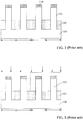
Figures 1-3 illustrate structures corresponding to certain stages of an existing fabrication process of a semiconductor structure; -
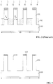
Figures 4-12 illustrate structures corresponding to certain stages of an exemplary fabrication process of a semiconductor structure consistent with the disclosed embodiments; and -
Figure 13 illustrates an exemplary fabrication process of a semiconductor structure consistent with the disclosed embodiments. - Reference will now be made in detail to exemplary embodiments of the invention, which are illustrated in the accompanying drawings. Wherever possible, the same reference numbers will be used throughout the drawings to refer to the same or like parts.
- With the continuous shrinking of the fin size of FinFETs, a punch through phenomenon is easy to occur between the bottoms of the source regions and the drain regions of the FinFETs. That is, a short-circuit is easy to occur between the bottoms of the source regions and the drain regions of the FinFET structures to thus generate leakage current. To overcome the punch through between the source regions and the drain regions of the FinFET structures, one approach is to implant reverse type ions in the bottom regions of the fins between the source regions and the drain regions to isolate the bottoms of the source regions and the drain regions.
-
Figures 1-3 illustrate structures corresponding to certain stages of an existing fabrication method of a semiconductor structure. As shown inFigure 1 , the method includes providing a base substrate. The base substrate includes asemiconductor substrate 100; and a plurality offins 101 formed on thesemiconductor substrate 100. Ahard mask layer 110 is formed on the tops of thefins 101. Thesemiconductor substrate 100 has a first transistor region A and a second transistor region B. - Further,
isolation structures 102 are formed among thefins 101. The top surfaces of theisolation structures 102 are below the top surfaces of thefins 101. - Further, as shown in
Figure 2 , an anti-punch through ion implantation process is performed to implant the anti-punch through ions in theisolation structures 102. Then, as shown inFigure 3 , after the anti-punch through ion implantation process, a thermal annealing process is performed to allow the anti-punch through ions to diffuse into the bottoms of thefins 101. - During the thermal annealing process, the anti-punch through ions may be easily diffused toward the tops of the fins 1 O 1. Thus, the threshold voltage of the subsequently formed transistors is increased. Accordingly, the performance of the transistors may be adversely affected.
- The present invention provides a semiconductor structure and a fabrication method thereof. The fabrication method includes providing a base substrate having a semiconductor substrate and a plurality of fins formed on the semiconductor substrate; and forming an anti-diffusion layer containing anti-diffusion ions in the fins. The method may also include forming an anti-punch through layer with a top surface below a top surface of the anti-diffusion layer in the fins; and performing a thermal annealing process. The anti-punch through layer may have anti-punch through ions. The anti-diffusion layer may be used to prevent the anti-punch through ions from diffusing toward the tops of the fins.
- In the disclosed methods, before performing the thermal annealing process, the anti-diffusion layer may be formed in the fins. The anti-diffusion layer may be able to prevent the anti-punch through ions from diffusing toward the tops of the fins during the thermal annealing process. Thus, the amount of the anti-punch through ions diffusing into the channel regions may be reduced. Therefore, the disclosed methods may be able to reduce the effects of the anti-punch through ions to the threshold voltage of the transistors; and the performance of the semiconductor structures may be enhanced.
-
Figure 13 illustrates an exemplary fabrication process of a semiconductor structure consistent with the disclosed embodiments.Figures 4-12 illustrate semiconductor structures corresponding to certain stages of the exemplary fabrication process. - As shown in
Figure 13 , at the beginning of the fabrication process, a base substrate with certain structures is provided (S101).Figure 4 illustrates a corresponding semiconductor structure. - As shown in
Figure 4 , a base substrate is provided. The base substrate may include asemiconductor substrate 200 and a plurality offins 201 formed on thesemiconductor substrate 200. - In one embodiment, the base substrate may have a first transistor region I and a second transistor region II. In some embodiments, the base substrate may only have a first transistor region, or a second transistor region.
- In one embodiment, the first transistor region I may be used to form NMOS transistors; and the second transistor region II may be used to form PMOS transistors. In another embodiment, the first transistor region may be used to form PMOS transistors; and the second transistor region II may be used to form NMOS transistors.
- In one embodiment, as shown in
Figure 4 , ahard mask layer 202 may be formed on the tops of thefins 201. Thehard mask layer 202 may be able to protect thefins 201 during the subsequent anti-punch through ion implantation process; and the effect of the anti-punch through ions to the transistors may be reduced. - In one embodiment, the process for forming the base substrate may include providing an initial substrate; forming the patterned
hard mask layer 202 on the initial substrate; and patterning the initial substrate using the patternedhard mask layer 202 as a mask. Thus, thesemiconductor substrate 200 and thefins 201 may be formed. Thefins 201 may be used to form the channel regions of the transistors. - Returning to
Figure 13 , after forming thefins 201, an initial isolation layer may be formed (S102).Figure 5 illustrates a corresponding semiconductor structure. - As shown in
Figure 5 , aninitial isolation layer 212 is formed over thesemiconductor substrate 200. The top surface of theinitial isolation layer 212 may be above the top surfaces of thefins 201. Theinitial isolation layer 212 may be used to subsequently form isolation structures. - The
initial isolation layer 212 may be made of any appropriate material(s), such as silicon oxide, or silicon oxynitride, etc. Various processes may be used to form theinitial isolation layer 212, such as a chemical vapor deposition (CVD) process, a physical vapor deposition (PVD) process, a flowable CVD (FCVD) process, or an atomic layer deposition (ALD) process, etc. - Returning to
Figure 13 , after forming theinitial isolation layer 202, initial isolation structures may be formed (S103).Figure 6 illustrates a corresponding semiconductor structure. - As shown in
Figure 6 , theinitial isolation structures 210 are formed among thefins 201. Theinitial isolation structures 210 may be formed by etching theinitial isolation layer 212 to cause the top surface of theinitial isolation layer 212 to be below the tops of thefins 201. Theinitial isolation structures 210 may be used as media for subsequently doping thefins 201. - In one embodiment, the
initial isolation structures 210 are made of a same material as that of theinitial isolation layer 212. That is, theinitial isolation structures 210 may be made of silicon oxide, or silicon oxynitride, etc. Various processes may be used to etch theinitial isolation layer 212, such as a dry etching process, or a wet etching process, etc. - Returning to
Figure 13 , after forming theinitial isolation structures 210, an anti-diffusion layer may be formed (S104).Figure 7 illustrates a corresponding semiconductor structure. - As shown in
Figure 7 , an anti-diffusion ion implantation process is performed to theinitial isolation structures 210; and ananti-diffusion layer 211 may be formed in thefins 201. Theanti-diffusion layer 211 may be used to prevent the anti-punch through ions in the subsequently formed anti-punch through layer from diffusing toward the tops of thefins 201. - The anti-diffusion ions may be implanted into the
initial isolation structures 210; and the anti-diffusion ions may be easy to diffuse into thefins 201. Thus, theanti-diffusion layer 211 may be formed in thefins 201. The anti-punch through layer may be subsequently formed under theanti-diffusion layer 211. Thus, theanti-diffusion layer 211 may be able to prevent the anti-punch through ions from diffusing toward the tops of thefins 201. - In one embodiment, the
anti-diffusion layer 211 may have anti-diffusion ions. The anti-diffusion ions may be the group IV ions. The electron number of the outer shell of the group IV elements may be identical to the electron number of the outer shell of the element of thefins 201. Thus, the anti-diffusion ions may be uneasy to form majority carriers in thefins 201. Accordingly, the conductivity of thefins 201 may not be changed. - Further, the anti-diffusion ions may be uneasy to form bonds with the atoms of the
fins 201. The ions uneasy to form bonds with the atoms of thefins 201 may be uneasy to be activated during the thermal annealing process. Thus, the anti-diffusion ions uneasy to form bonds with the atoms of thefins 201 may not change the conductivity of thefins 201. - Further, the anti-diffusion ions may enter into interstitial lattice sites of the atoms of the
fins 201. Thus, theanti-diffusion layer 211 may be able to prevent the anti-punch through ions of the subsequently formed anti-punch through layer from interstitially diffusing toward the tops of thefins 201. Accordingly, the performance of the semiconductor structure may be improved. - In one embodiment, the anti-diffusion ions include one or more types of C ions, Ge ions and N ions. After the C ions, G ions and N ions enter into the interstitial sites of the atoms of the
fins 201, they may be able to prevent the anti-punch through ions from diffusing toward the tops of thefins 201. Further, the N atoms may be uneasy to activate during the thermal annealing process. Thus, they may not affect the conductivity of thefins 201. The C ions and Ge ions are group IV elements, they may also be uneasy to activate; and may be uneasy to affect the conductivity of thefins 201. - The thickness of the
anti-diffusion layer 211 may be any appropriate value. If the thickness of theanti-diffusion layer 211 is too large, the conductivity of thefins 201 may be affected; and the performance of the transistors may be reduced. If the thickness of theanti-diffusion layer 211 is too small, it may be difficult to prevent the anti-punch through ions from diffusing toward the tops of thefins 201. Thus, in one embodiment, the thickness of theanti-diffusion layer 211 may be in a range of approximately 10Å-50Å. - The doping concentration of the
anti-diffusion layer 211 may be any appropriate value. If the concentration is too high, the conductivity of thefins 201 may be easily affected; and the performance of the transistors may be reduced. If the concentration is too low, it may be difficult to prevent the anti-punch through ions from diffusing toward the tops of thefins 201. Thus, in one embodiment, the concentration of the anti-diffusion ions of theanti-diffusion layer 211 may be in a range of approximately 1.0E13 atoms/cm2-1.0E16 atoms/cm2. - In one embodiment, the energy of the anti-diffusion ion implantation process may be in a range of approximately 1 KeV-300 KeV. The dosage of the anti-diffusion ion implantation process may be in a range of approximately 1.0E12 atoms/cm2-1.0E16 atoms/cm2.
- Returning to
Figure 13 , after forming theanti-diffusion layer 211, isolation structures may be formed (S105).Figure 8 illustrates a corresponding semiconductor structure. - As shown in
Figure 8 , a partial thickness of the initial isolation structures 210 (referring toFigure 7 ) are removed; and theisolation structures 213 may be formed. Theisolation structures 213 may be used as media for subsequently performing an anti-punch through ion implantation process. - By removing the partial thickness of the
initial isolation structures 210, the top surfaces of theisolation structures 213 may be lower than theinitial isolation structures 210. Correspondingly, the top surface of the subsequently formed anti-punch through layer may be below the top surface of theanti-diffusion layer 211. Thus, theanti-diffusion layer 211 may be able to prevent the anti-punch through ions from diffusing toward the tops of thefins 201. - The removed partial thickness of the
initial structures 210 may be any appropriate value. If the removed partial thickness is too large, the subsequently formed anti-punch through layer and theanti-diffusion layer 211 may have a relatively large distance. The anti-punch through ions may be easy to diffuse into the portions of thefins 201 between the anti-punch through layer and theanti-diffusion layer 211; and the performance of the semiconductor structures may be affected. If the removed partial thickness is too small, the thickness of theanti-diffusion layer 211 on the anti-punch through layer may be relatively small; theanti-diffusion barrier layer 211 may be unable to prevent the anti-punch through ions from diffusing toward the tops of thefins 201. Thus, in one embodiment, the removed partial thickness may be in a range of approximately 15Å-60Å. - In one embodiment, as shown in
Figure 8 , the top surfaces of theisolation structures 213 level with the bottom surface of theanti-diffusion layer 211. Correspondingly, the top surface of the subsequently formed anti-punch through layer may level with the bottom surface of theanti-diffusion layer 211. - In some embodiments, the top surface of the anti-punch through layer may be below the bottom surface of the anti-diffusion layer; or the top surface of the anti-punch through layer is above the top surface of the anti-diffusion layer and the bottom surface of the anti-punch through layer is below the top surface of the anti-diffusion layer.
- Various processes may be used to remove the partial thickness of the
initial isolation structures 210, such as a dry etching process, or a wet etching process, etc. - Returning to
Figure 13 , after forming theisolation structures 213, an anti-punch through layer may be formed (S106).Figures 9-10 illustrate corresponding semiconductor structures. - As shown in
Figures 9-10 , an anti-punch through layer is formed. In one embodiment, the base substrate includes the first transistor region I and the second transistor region II. Thus, the anti-punch through layer may include a first anti-punch throughlayer 221 in the first transistor region I and a second punch throughlayer 222 in the second transistor region II under theanti-diffusion layer 211. In some embodiments, the base substrate may only include a first transistor region or a second transistor region, the anti-punch layer may be one layer. - The anti-punch through layer may be formed by performing one or more steps of anti-punch through ion implantation process on the
isolation structures 213. The anti-punch through ions implanted into theisolation structures 213 may diffuse into thefins 201 to form the anti-punch through layer. The anti-punch through layer may be able to reduce the punch through probability between the source regions and the drain regions of the transistors. - In one embodiment, as shown in
Figures 9-10 , the top surface of the anti-punch through layer may be below the top surface of theanti-diffusion layer 211. The anti-punch through layer may have the anti-punch through ions. Thus, theanti-diffusion layer 211 may be able to prevent the anti-punch through ions from diffusing toward the tops of thefins 201. The anti-punch through layer may be used to reduce the source-drain punch through probability of the transistors; and reduce the leakage current in the channel regions of the transistors. - Referring to
Figures 9-10 , because the base substrate may include the first transistor region I and the second transistor region II, the anti-punch through ion implantation process may include performing a first anti-punch through ion implantation process to theisolation structures 213 in the first transistor region I to form the first anti-punch throughlayer 221; and performing a second anti-punch through ion implantation process to theisolation structures 213 in the second region II to form the second anti-punch throughlayer 222. - In some embodiments, the base substrate may only include the first transistor region and the second transistor region. Thus, the anti-punch through ion implantation process may only include a first anti-punch through ion implantation process performed on the isolation structures in the first transistor region to form a first anti-punch through layer, or a second anti-punch through ion implantation process performed on the isolation structures in the second transistor region to form a second anti-punch through layer.
- Specifically, as shown in
Figure 9 , the first anti-punch through ion implantation process is performed on theisolation structures 211 in the first transistor region I; and the first anti-punch throughlayer 221 may be formed in thefins 201 in the first transistor region I. The first anti-punch throughlayer 221 may be used to reduce the source-drain punch through probability in the transistors in the first transistor region I. - The first anti-punch through ion implantation process may include forming a
first photoresist layer 231 over the second transistor region II; and performing the first anti-punch through ions implantation process using thefirst photoresist layer 231 as a mask. Thus, the first anti-punch throughlayer 221 may be formed in thefins 201 in the first region I. - The ions implanted into the
isolation structures 211 to form the first anti-punch throughlayer 221, i.e., the ions in the first anti-punch throughlayer 211, may be referred to as first anti-punch through ions. In one embodiment, the first transistor region I may be used to form NMOS transistors, the first anti-punch through ions may be B ions, or F ions, etc. In some embodiments, the first transistor region I may be used to form PMOS transistors, the first anti-punch through ions may be P ions, or As ions. - The thickness of the first anti-punch through
layer 221 may be any appropriate value. If the thickness of the first anti-punch throughlayer 221 is too large, it may be easy to have a material waste issue. If the thickness of the first anti-punch throughlayer 221 is too small, it may be difficult to achieve the anti-punch through function. Thus, in one embodiment, the thickness of the first anti-punch throughlayer 221 is in a range of approximately 20Å-60Å. - The concentration of the anti-punch through ions in the first anti-punch through
layer 221 may be any appropriate value. If the concentration of the anti-punch through ions in the first anti-punch throughlayer 221 is too high, the anti-punch through ions may be easy to punch through theanti-diffusion layer 211 to diffuse toward the tops of thefins 201; and the performance of the transistors may be affected. If the concentration of the anti-punch through ions in the first anti-punch throughlayer 221 is too low, the anti-punch through function of the anti-punch throughlayer 221 may not be achieved. That is, the first anti-punch throughlayer 221 may be unable to prevent the punch through between the source regions and the drain regions of the transistors. Thus, in one embodiment, the concentration of the anti-punch through ions in the first anti-punch throughlayer 221 may be in a range of approximately 1.0E13 atoms/cm3-1.0E15 atoms/cm3. - In one embodiment, the dosage of the first anti-punch through ion implantation process may be in a range of approximately 1.0E13atoms/cm2-1.0E15atoms/cm2. The energy of the first anti-punch through ion implantation process may be in a range of 5 keV-100 keV.
- Further, as shown in
Figure 10 , after performing the first anti-punch through ion implantation process, the second anti-punch through ion implantation process is performed on theisolation structures 213 in the second transistor region II; and the second anti-punch throughlayer 222 may be formed in thefins 201 in the second transistor region II. The second anti-punch throughlayer 222 may be used to reduce the source-drain punch through probability in the transistors in the second transistor region II. - The second anti-punch through ion implantation process may include forming a
second photoresist layer 232 over the first transistor region I; and performing the second anti-punch through ions implantation process using thesecond photoresist layer 232 as a mask. Thus, the second anti-punch throughlayer 222 may be formed in thefins 201 in the second region II. - The ions implanted into the
isolation structures 213 to form the second anti-punch throughlayer 222, i.e., the ions in the second anti-punch throughlayer 222, may be referred to as second anti-punch through ions. In one embodiment, the second transistor region II may be used to form PMOS transistors, the second anti-punch through ions may be P ions, or As ions, etc. In some embodiments, the second transistor region II may be used to form NMOS transistors, the second anti-punch through ions may be B ions, or F ions. - The thickness of the second anti-punch through
layer 222 may be any appropriate value. If the thickness of the second anti-punch throughlayer 222 is too large, it may be easy to have a material waste issue. If the thickness of the second anti-punch throughlayer 222 is too small, it may be difficult to achieve the anti-punch through function. Thus, in one embodiment, the thickness of the second anti-punch throughlayer 222 is in a range of approximately 20Å-60Å. - The concentration of the second anti-punch through ions in the second anti-punch through
layer 222 may be any appropriate value. If the concentration of the second anti-punch through ions in the second anti-punch throughlayer 222 is too high, the second anti-punch through ions may be easy to punch through theanti-diffusion layer 211 to diffuse toward the tops of thefins 201; and the performance of the transistors may be affected. If the concentration of the second anti-punch through ions in the second anti-punch throughlayer 222 is too low, the anti-punch through function of the second anti-punch throughlayer 222 may not be achieved. That is, the second anti-punch throughlayer 222 may be unable to prevent the punch through between the source regions and the drain regions of the transistors. Thus, in one embodiment, the concentration of the second anti-punch through ions in the second anti-punch throughlayer 222 may be in a range of approximately 1.0E13 atoms/cm3-1.0E15 atoms/cm3. - In one embodiment, the dosage of the second anti-punch through ion implantation process may be in a range of approximately 1.0E13 atoms/cm2-1.0E15 atoms/cm2. The energy of the second anti-punch through ion implantation process may be in a range of 5 keV-100 keV.
- In one embodiment, the top surface of the anti-punch through layer levels with the bottom surface of the anti-diffusion layer. In some embodiments, the top surface of the anti-punch through layer may be below the bottom surface of the anti-diffusion layer. In other embodiments, the top surface of the anti-punch through layer may be above the top surface of the anti-diffusion layer; and the bottom surface of the anti-punch through layer be below the top surface of the anti-diffusion layer.
- Returning to
Figure 13 , after forming the anti-punch through layer, a thermal annealing process may be performed (S107).Figure 11 illustrates a corresponding semiconductor structure. - As shown in
Figure 11 , a thermal annealing process is performed to activate the anti-punch through ions. The activated anti-punch through ions may be able to prevent the source-drain punch through. - During the thermal annealing process, the
anti-diffusion layer 211 may be able to prevent the anti-punch through ions in the anti-punch through layer from diffusing toward the tops of thefins 201. The effect of the anti-punch through ions to the transistors may be reduced; and the performance of the semiconductor structure may be improved. - The temperature of the thermal annealing process may be any appropriate value. In one embodiment, the temperature of the thermal annealing process may be in a range of approximately 950°C-1050°C.
- After the thermal annealing process, as shown in
Figure 12 , agate structure 230 crossing over thefins 201 may be formed. Thegate structure 230 may cover portions of the side and top surfaces of thefins 201. - In some embodiments, before forming the anti-diffusion layer and the anti-punch through layer, isolation structures may be formed over the base substrate. The top surfaces of the isolation structures may be lower than the top surfaces of the fins.
- Then, an anti-punch through ion implantation process may be performed on the isolations structures. Thus, the anti-punch through layer may be formed in the fins.
- After forming the anti-punch through layer, a doping layer may be formed on the isolation structures. The doping layer may have anti-diffusion ions.
- The doping layer may be formed by a CVD process. During the CVD process, the anti-diffusion ions may be doped into the doping layer, and the anti-diffusion ions may diffuse into the fins; and the anti-diffusion layer may be formed in the fins. In one embodiment, the doping layer may be made of silicon oxide doped with the anti-diffusion ions.
- In other embodiments, after forming the anti-diffusion layer, the doping layer may be removed to expose the surfaces of the isolation structures. After removing the doping layer, an anti-punch through ion implantation process may be performed on the isolation structures to form the anti-punch through layer.
- Thus, according to the disclosed fabrication methods of the semiconductor structure, before the thermal annealing process, an anti-diffusion layer may be formed in the fins. The anti-diffusion layer may be able to prevent the anti-punch through ions from diffusing toward the tops of the fins. Thus, the amount of the anti-punch through ions diffusing into the channel regions of the transistors may be reduced. Accordingly, the disclosed methods for fabricating the semiconductor structures may be able to reduce the effect of the anti-punch through ions to the threshold voltage of the transistors. Therefore, the performance of the semiconductor structure may be improved.
- Thus, a semiconductor structure may be formed by the disclosed methods and processes.
Figure 12 illustrates a corresponding semiconductor structure. - As shown in
Figure 12 , the semiconductor structure includes a base substrate having asemiconductor substrate 200 and a plurality offins 201 formed on thesemiconductor substrate 200; ananti-diffusion layer 211 having anti-diffusion ions formed in thefins 201; and an anti-punch through layer including a first anti-punch throughlayer 221 forming the fins in the first transistor region I and a second anti-punch throughlayer 222 formed in thefins 201 in the second transistor region II. The bottom surface of the anti-punch through layer may be below the top surface of theanti-diffusion layer 211. The anti-punch through layer may have anti-punch through ions; and theanti-diffusion layer 211 may be used to prevent the anti-punch through ions from diffusing toward the tops of thefins 201. - In one embodiment, the base substrate may include a first transistor region I and a second transistor region II. In some embodiments, the base substrate may only include a first transistor region, or a second transistor region.
- In one embodiment, the first transistor region I may be used to form NMOS transistors; and the second transistor region II may be used to form PMOS transistors. In some embodiments, the first transistor region may be used to form PMOS transistors; and the second transistor region may be used to form NMOS transistors.
- In one embodiment, a
hard mask layer 202 may be formed on the tops of thefins 201. Thehard mask layer 202 may be able to protect thefins 201 during the subsequent anti-punch through ion implantation process; and the effect of the anti-punch through ions to the transistors may be reduced. - In one embodiment, the
anti-diffusion layer 211 may have anti-diffusion ions. The anti-diffusion ions may be the group IV ions, or the element uneasy to form bonds with the fins. The electron number of the outer shell of the group IV element may be identical to the electron number of the most out shell of the element of thefins 201. Thus, the anti-diffusion ions may be uneasy to form majority carriers in thefins 201. Accordingly, the conductivity of thefins 201 may not be changed. - Further, the anti-diffusion ions may be uneasy to form bonds with the atoms of the
fins 201. The ions uneasy to form bonds with the atoms of thefins 201 may be uneasy to activate during the thermal annealing process. Thus, the anti-diffusion ions uneasy to form bonds with the atoms of thefins 201 may not change the conductivity of thefins 201. - Further, the anti-diffusion ions may enter into interstitial lattice sites of the atoms of the
fins 201. Thus, theanti-diffusion layer 211 may be able to prevent the anti-punch through ions of the subsequently formed anti-punch through layer from interstitially diffusing toward the tops of thefins 201. Accordingly, the performance of the semiconductor structure may be improved. - The
anti-diffusion layer 211 may be able to prevent the anti-punch through ions from diffusing toward the tops of thefins 201 during the subsequent thermal annealing process. Thus, the amount of the anti-punch through ions diffusing into the channel regions of the transistors may be reduced; and the effect of the anti-punch through ions to the threshold voltage of the transistors may be reduced. Therefore, the performance of the semiconductor structure may be improved. - The thickness of the
anti-diffusion layer 211 may be any appropriate value. If the thickness of theanti-diffusion layer 211 is too large, the conductivity of thefins 201 may be affected; and the performance of the transistors may be reduced. If the thickness of theanti-diffusion layer 211 is too small, it may be difficult to prevent the anti-punch through ions from diffusing toward the tops of thefins 201. Thus, in one embodiment, the thickness of theanti-diffusion layer 211 may be in a range of approximately 10Å-50Å. - The doping concentration of the
anti-diffusion layer 211 may be any appropriate value. If the concentration is too high, the conductivity of thefins 201 may be easily affected; and the performance of the transistors may be reduced. If the concentration is too low, it may be difficult to prevent the anti-punch through ions from diffusing toward the tops of thefins 201. Thus, in one embodiment, the concentration of the anti-diffusion ions of theanti-diffusion layer 211 may be in a range of approximately 1.0E13atoms/cm2- 1.0E16atoms/cm2. - In one embodiment, the base substrate includes the first transistor region I and the second transistor region II. Thus, the anti-punch through layer may include the first anti-punch through
layer 221 in the first region I and a second punch throughlayer 222 in the second transistor region II under theanti-diffusion layer 211. The first anti-punch throughlayer 221 may have first anti-punch through ions; and the second anti-punch throughlayer 222 may have second anti-punch through ions. In some embodiments, the base substrate may only include a first transistor region, or a second transistor region, the anti-punch layer may be one layer: a first anti-punch through layer in the first transistor region, or a second anti-punch through layer in the second transistor region. - In one embodiment, the first transistor region I may be used to form NMOS transistors, the first anti-punch through ions may be B ions, or F ions, etc. In some embodiments, the first transistor region I may be used to form PMOS transistors, the first anti-punch through ions may be P ions or As ions.
- The thickness of the first anti-punch through
layer 221 may be any appropriate value. If the thickness of the first anti-punch throughlayer 221 is too large, it may be easy to have a material waste issue. If the thickness of the first anti-punch throughlayer 221 is too small, it may be difficult to achieve the anti-punch through function. Thus, in one embodiment, the thickness of the first anti-punch throughlayer 221 is in a range of approximately 20Å-60Å. - The concentration of the anti-punch through ions in the first anti-punch through
layer 221 may be any appropriate value. If the concentration of the anti-punch through ions in the first anti-punch throughlayer 221 is too high, the anti-punch through ions may be easy to punch through theanti-diffusion layer 211 to diffuse toward the tops of thefins 201; and the performance of the transistors may be affected. If the concentration of the anti-punch through ions in the first anti-punch throughlayer 221 is too low, the anti-punch through function of the anti-punch throughlayer 221 may not be achieved. That is, the first anti-punch throughlayer 221 may be unable to prevent the punch through between the source regions and the drain regions of the transistors. Thus, in one embodiment, the concentration of the anti-punch through ions in the first anti-punch throughlayer 221 may be in a range of approximately 1.0E13 atoms/cm3-1.0E15 atoms/cm3. - The second anti-punch through
layer 222 may be used to reduce the source-drain punch through probability in the transistors in the second transistor region II. In one embodiment, the second transistor region II may be used to form PMOS transistors, the second anti-punch through ions may be P ions, or As ions, etc. In some embodiments, the second transistor region II may be used to form NMOS transistors, the second anti-punch through ions may be B ions or F ions. - The thickness of the second anti-punch through
layer 222 may be any appropriate value. If the thickness of the second anti-punch throughlayer 222 is too large, it may be easy to have a material waste issue. If the thickness of the second anti-punch throughlayer 222 is too small, it may be difficult to achieve the anti-punch through function. Thus, in one embodiment, the thickness of the second anti-punch throughlayer 222 is in a range of approximately 20Å-60Å. - The concentration of the second anti-punch through ions in the second anti-punch through
layer 222 may be any appropriate value. If the concentration of the second anti-punch through ions in the second anti-punch throughlayer 222 is too high, the second anti-punch through ions may be easy to punch through theanti-diffusion layer 211 to diffuse toward the tops of thefins 201; and the performance of the transistors may be affected. If the concentration of the second anti-punch through ions in the second anti-punch throughlayer 222 is too low, the anti-punch through function of the second anti-punch throughlayer 222 may not be achieved. That is, the second anti-punch throughlayer 222 may be unable to prevent the punch through between the source regions and the drain regions of the transistors. Thus, in one embodiment, the concentration of the second anti-punch through ions in the second anti-punch throughlayer 222 may be in a range of approximately 1.0E13atoms/cm3-1.0E15atoms/cm3. - To cause the
anti-diffusion layer 211 to be able to prevent the anti-punch through ions from diffusing toward the tops of thefins 201, the top surface of the anti-punch layer may be below the top surface of theanti-diffusion layer 211. Specially, in one embodiment, the top surface of the anti-punch through layer levels with the top surface of theanti-diffusion layer 211. - In some embodiments, the top surface of the anti-punch through layer may be below the bottom surface of the anti-diffusion layer. In other embodiments, the top surface of the anti-punch through layer may be above the top surface of the anti-diffusion layer; and the bottom surface of the anti-punch through layer may be below the top surface of the anti-diffusion layer.
- If the distance between the top surface of the anti-punch through layer and the top surface of the
anti-diffusion layer 211 is too large, the top surface of the anti-punch through layer and the bottom surface of theanti-diffusion layer 211 may have a relatively large distance. The anti-punch through ions may be easy to diffuse into the portions of thefins 201 between the anti-punch through layer and theanti-diffusion layer 211; and the performance of the semiconductor structure may be affected. If the distance between the top surface of the anti-punch through layer and the top surface of theanti-diffusion layer 211 is too small, the thickness of the portion of theanti-diffusion layer 211 on the anti-punch through layer may be relatively small, theanti-diffusion barrier layer 211 may be unable to prevent the anti-punch through ions from diffusing toward the tops of thefins 201. Thus, in one embodiment, the distance between the top surface of the anti-punch through layer and the top surface of theanti-diffusion layer 211 may be in a range of approximately 10Å-40Å. - Further, the semiconductor structure may also include
isolation structures 213 formed on thesemiconductor substrate 200. Theisolation structures 213 may be used to electrically insulate thefins 201. - In one embodiment, the top surfaces of the
isolation structures 213 may be above the top surface of the anti-punch through layer, or level with the top surface of the anti-punch through layer. In one embodiment, the top surfaces of theisolation structures 213 level with the top surface of the anti-punch through layer. If the top surfaces of theisolation structures 213 are below the top surface of the anti-punch through layer, the doping ions in the channel regions of the transistor may diffuse into the anti-punch through layer. The anti-punch through ions may be verse-type ions; and may be easy to increase the threshold voltage of the transistors. In one embodiment, theisolation structures 213 may be made of silicon oxide, or silicon oxynitride. - Further, the semiconductor structures may also include a gate structure crossing over the
fins 201. Thegate structure 230 may cover portions of side and top surfaces of thefins 201. - Therefore, according to the disclosed embodiments, an anti-diffusion layer may be formed in the fins. The anti-diffusion layer may be able to prevent the anti-punch through ions from diffusing toward the tops of the fins during the thermal annealing process. Thus, the anti-punch through ions diffusing into the channel regions of the transistors may be reduced; and the performance of the semiconductor structure may be improved.
Claims (14)
Applications Claiming Priority (1)
| Application Number | Priority Date | Filing Date | Title |
|---|---|---|---|
| CN201610531674.3A CN107591328A (en) | 2016-07-07 | 2016-07-07 | Semiconductor structure and forming method thereof |
Publications (1)
| Publication Number | Publication Date |
|---|---|
| EP3267476A1 true EP3267476A1 (en) | 2018-01-10 |
Family
ID=59296764
Family Applications (1)
| Application Number | Title | Priority Date | Filing Date |
|---|---|---|---|
| EP17179929.9A Withdrawn EP3267476A1 (en) | 2016-07-07 | 2017-07-06 | Semiconductor structure and fabrication method thereof |
Country Status (3)
| Country | Link |
|---|---|
| US (1) | US10002869B2 (en) |
| EP (1) | EP3267476A1 (en) |
| CN (1) | CN107591328A (en) |
Families Citing this family (6)
| Publication number | Priority date | Publication date | Assignee | Title |
|---|---|---|---|---|
| CN107799421B (en) * | 2016-09-05 | 2021-04-02 | 中芯国际集成电路制造(上海)有限公司 | Method of forming a semiconductor device |
| CN110660656A (en) * | 2019-09-30 | 2020-01-07 | 上海华力集成电路制造有限公司 | P-type well ion implantation method, P-type well structure and CMOS device fabrication method |
| CN113808996B (en) * | 2020-06-12 | 2025-09-16 | 中芯国际集成电路制造(上海)有限公司 | Semiconductor structure and forming method thereof |
| CN115249745B (en) * | 2021-04-27 | 2026-04-21 | 中芯国际集成电路制造(上海)有限公司 | Semiconductor structure and its formation method |
| CN113571418B (en) * | 2021-05-31 | 2024-03-08 | 上海华力集成电路制造有限公司 | A method of forming super wells for FinFET |
| CN116137284A (en) * | 2021-11-18 | 2023-05-19 | 上海集成电路装备材料产业创新中心有限公司 | Semiconductor device and manufacturing method thereof |
Citations (1)
| Publication number | Priority date | Publication date | Assignee | Title |
|---|---|---|---|---|
| US8497171B1 (en) * | 2012-07-05 | 2013-07-30 | Taiwan Semiconductor Manufacturing Co., Ltd. | FinFET method and structure with embedded underlying anti-punch through layer |
Family Cites Families (5)
| Publication number | Priority date | Publication date | Assignee | Title |
|---|---|---|---|---|
| CN103855015B (en) * | 2012-11-30 | 2020-03-06 | 中国科学院微电子研究所 | FinFET and manufacturing method thereof |
| US8969932B2 (en) * | 2012-12-12 | 2015-03-03 | Globalfoundries Inc. | Methods of forming a finfet semiconductor device with undoped fins |
| US20150255456A1 (en) * | 2014-03-04 | 2015-09-10 | Globalfoundries Inc. | Replacement fin insolation in a semiconductor device |
| US9312389B2 (en) * | 2014-05-23 | 2016-04-12 | Broadcom Corporation | FinFET with undoped body bulk |
| US9299618B1 (en) * | 2014-09-24 | 2016-03-29 | International Business Machines Corporation | Structure and method for advanced bulk fin isolation |
-
2016
- 2016-07-07 CN CN201610531674.3A patent/CN107591328A/en active Pending
-
2017
- 2017-04-24 US US15/494,691 patent/US10002869B2/en active Active
- 2017-07-06 EP EP17179929.9A patent/EP3267476A1/en not_active Withdrawn
Patent Citations (1)
| Publication number | Priority date | Publication date | Assignee | Title |
|---|---|---|---|---|
| US8497171B1 (en) * | 2012-07-05 | 2013-07-30 | Taiwan Semiconductor Manufacturing Co., Ltd. | FinFET method and structure with embedded underlying anti-punch through layer |
Non-Patent Citations (1)
| Title |
|---|
| OKANO K ET AL: "Process integration technology and device characteristics of CMOS FinFET on bulk silicon substrate with sub-10 nm fin width and 20 nm gate length", INTERNATIONAL ELECTRON DEVICES MEETING 5-7.12.2005, IEEE, IEEE, PISCATAWAY, NJ. USA, 5 December 2005 (2005-12-05), pages 721 - 724, XP010903585, ISBN: 978-0-7803-9268-7, DOI: 10.1109/IEDM.2005.1609454 * |
Also Published As
| Publication number | Publication date |
|---|---|
| US20180012888A1 (en) | 2018-01-11 |
| US10002869B2 (en) | 2018-06-19 |
| CN107591328A (en) | 2018-01-16 |
Similar Documents
| Publication | Publication Date | Title |
|---|---|---|
| US9245975B2 (en) | Recessed channel insulated-gate field effect transistor with self-aligned gate and increased channel length | |
| US9117842B2 (en) | Methods of forming contacts to source/drain regions of FinFET devices | |
| US10002869B2 (en) | Semiconductor structure and fabrication method thereof | |
| US9263549B2 (en) | Fin-FET transistor with punchthrough barrier and leakage protection regions | |
| US9450078B1 (en) | Forming punch-through stopper regions in finFET devices | |
| US9059210B2 (en) | Enhanced stress memorization technique for metal gate transistors | |
| CN107919324B (en) | Method of forming a semiconductor device | |
| US10256243B2 (en) | Semiconductor structure, static random access memory, and fabrication method thereof | |
| US20160126327A1 (en) | Method of making a split gate memory cell | |
| US8835270B2 (en) | Dual NSD implants for reduced Rsd in an NMOS transistor | |
| US20100102399A1 (en) | Methods of Forming Field Effect Transistors and Devices Formed Thereby | |
| KR20160012459A (en) | Semiconductor device and method of manufacturing the same | |
| CN114121659B (en) | Preparation method of semiconductor device | |
| US11121237B2 (en) | Manufacturing method for FinFET device | |
| US10418461B2 (en) | Semiconductor structure with barrier layers | |
| US10177246B2 (en) | Semiconductor structure and fabrication method thereof | |
| CN107785425B (en) | Semiconductor device and method of forming the same | |
| US9627524B2 (en) | High voltage metal oxide semiconductor device and method for making same | |
| US10727130B2 (en) | Semiconductor device and fabrication method thereof | |
| CN109427681B (en) | Semiconductor structure and method of forming the same | |
| CN112466950B (en) | An anti-edge leakage SOI MOS structure and its formation method | |
| US7790545B2 (en) | Semiconductor device having a polysilicon electrode including amorphizing, recrystallising, and removing part of the polysilicon electrode | |
| CN107591330B (en) | Method for forming semiconductor structure | |
| KR20150097946A (en) | Methods of manufacturing semiconductor devices | |
| KR100853982B1 (en) | 3D field effect transistor and its manufacturing method |
Legal Events
| Date | Code | Title | Description |
|---|---|---|---|
| PUAI | Public reference made under article 153(3) epc to a published international application that has entered the european phase |
Free format text: ORIGINAL CODE: 0009012 |
|
| STAA | Information on the status of an ep patent application or granted ep patent |
Free format text: STATUS: THE APPLICATION HAS BEEN PUBLISHED |
|
| AK | Designated contracting states |
Kind code of ref document: A1 Designated state(s): AL AT BE BG CH CY CZ DE DK EE ES FI FR GB GR HR HU IE IS IT LI LT LU LV MC MK MT NL NO PL PT RO RS SE SI SK SM TR |
|
| AX | Request for extension of the european patent |
Extension state: BA ME |
|
| STAA | Information on the status of an ep patent application or granted ep patent |
Free format text: STATUS: REQUEST FOR EXAMINATION WAS MADE |
|
| 17P | Request for examination filed |
Effective date: 20180316 |
|
| RBV | Designated contracting states (corrected) |
Designated state(s): AL AT BE BG CH CY CZ DE DK EE ES FI FR GB GR HR HU IE IS IT LI LT LU LV MC MK MT NL NO PL PT RO RS SE SI SK SM TR |
|
| RAP1 | Party data changed (applicant data changed or rights of an application transferred) |
Owner name: SEMICONDUCTOR MANUFACTURING INTERNATIONAL (BEIJING Owner name: SEMICONDUCTOR MANUFACTURING INTERNATIONAL (SHANGHA |
|
| STAA | Information on the status of an ep patent application or granted ep patent |
Free format text: STATUS: EXAMINATION IS IN PROGRESS |
|
| 17Q | First examination report despatched |
Effective date: 20210122 |
|
| STAA | Information on the status of an ep patent application or granted ep patent |
Free format text: STATUS: THE APPLICATION IS DEEMED TO BE WITHDRAWN |
|
| 18D | Application deemed to be withdrawn |
Effective date: 20210602 |