EP3267465B1 - Method and apparatus of detecting a condition in a plasma dicing process - Google Patents
Method and apparatus of detecting a condition in a plasma dicing process Download PDFInfo
- Publication number
- EP3267465B1 EP3267465B1 EP17179411.8A EP17179411A EP3267465B1 EP 3267465 B1 EP3267465 B1 EP 3267465B1 EP 17179411 A EP17179411 A EP 17179411A EP 3267465 B1 EP3267465 B1 EP 3267465B1
- Authority
- EP
- European Patent Office
- Prior art keywords
- dicing
- plasma
- substrate
- infrared emission
- end point
- Prior art date
- Legal status (The legal status is an assumption and is not a legal conclusion. Google has not performed a legal analysis and makes no representation as to the accuracy of the status listed.)
- Active
Links
- 238000000034 method Methods 0.000 title claims description 101
- 230000008569 process Effects 0.000 title claims description 75
- 239000000758 substrate Substances 0.000 claims description 85
- 229910052710 silicon Inorganic materials 0.000 claims description 27
- 239000010703 silicon Substances 0.000 claims description 27
- 238000001514 detection method Methods 0.000 claims description 20
- 238000001020 plasma etching Methods 0.000 claims description 13
- 238000005530 etching Methods 0.000 claims description 12
- 238000013459 approach Methods 0.000 claims description 11
- 230000004044 response Effects 0.000 claims description 6
- 239000004065 semiconductor Substances 0.000 claims description 5
- 229910001218 Gallium arsenide Inorganic materials 0.000 claims description 3
- 229910002601 GaN Inorganic materials 0.000 claims 1
- 230000001419 dependent effect Effects 0.000 claims 1
- 235000012431 wafers Nutrition 0.000 description 49
- XUIMIQQOPSSXEZ-UHFFFAOYSA-N Silicon Chemical compound [Si] XUIMIQQOPSSXEZ-UHFFFAOYSA-N 0.000 description 26
- 239000000463 material Substances 0.000 description 19
- 239000010410 layer Substances 0.000 description 9
- 230000003287 optical effect Effects 0.000 description 8
- 125000004122 cyclic group Chemical group 0.000 description 7
- 239000007789 gas Substances 0.000 description 7
- 238000005137 deposition process Methods 0.000 description 5
- 238000009826 distribution Methods 0.000 description 5
- 238000006243 chemical reaction Methods 0.000 description 4
- 229910052751 metal Inorganic materials 0.000 description 4
- 239000002184 metal Substances 0.000 description 4
- 238000012544 monitoring process Methods 0.000 description 4
- 239000004411 aluminium Substances 0.000 description 3
- 229910052782 aluminium Inorganic materials 0.000 description 3
- XAGFODPZIPBFFR-UHFFFAOYSA-N aluminium Chemical compound [Al] XAGFODPZIPBFFR-UHFFFAOYSA-N 0.000 description 3
- 239000006227 byproduct Substances 0.000 description 3
- 238000010943 off-gassing Methods 0.000 description 3
- 238000009623 Bosch process Methods 0.000 description 2
- 230000015572 biosynthetic process Effects 0.000 description 2
- 230000015556 catabolic process Effects 0.000 description 2
- 230000008859 change Effects 0.000 description 2
- 239000000470 constituent Substances 0.000 description 2
- 238000000151 deposition Methods 0.000 description 2
- 230000008021 deposition Effects 0.000 description 2
- 230000004907 flux Effects 0.000 description 2
- 239000011521 glass Substances 0.000 description 2
- 230000001939 inductive effect Effects 0.000 description 2
- 238000001465 metallisation Methods 0.000 description 2
- 238000002161 passivation Methods 0.000 description 2
- 229920000642 polymer Polymers 0.000 description 2
- 238000012545 processing Methods 0.000 description 2
- 230000035945 sensitivity Effects 0.000 description 2
- 239000000126 substance Substances 0.000 description 2
- 230000036962 time dependent Effects 0.000 description 2
- 238000012546 transfer Methods 0.000 description 2
- ZAMOUSCENKQFHK-UHFFFAOYSA-N Chlorine atom Chemical compound [Cl] ZAMOUSCENKQFHK-UHFFFAOYSA-N 0.000 description 1
- 239000004593 Epoxy Substances 0.000 description 1
- YCKRFDGAMUMZLT-UHFFFAOYSA-N Fluorine atom Chemical compound [F] YCKRFDGAMUMZLT-UHFFFAOYSA-N 0.000 description 1
- 229910004014 SiF4 Inorganic materials 0.000 description 1
- 230000001154 acute effect Effects 0.000 description 1
- 239000012790 adhesive layer Substances 0.000 description 1
- 230000004075 alteration Effects 0.000 description 1
- OEYOHULQRFXULB-UHFFFAOYSA-N arsenic trichloride Chemical compound Cl[As](Cl)Cl OEYOHULQRFXULB-UHFFFAOYSA-N 0.000 description 1
- 238000013473 artificial intelligence Methods 0.000 description 1
- 229910052801 chlorine Inorganic materials 0.000 description 1
- 239000000460 chlorine Substances 0.000 description 1
- 238000007796 conventional method Methods 0.000 description 1
- 239000002826 coolant Substances 0.000 description 1
- 238000001816 cooling Methods 0.000 description 1
- 230000000694 effects Effects 0.000 description 1
- 238000004100 electronic packaging Methods 0.000 description 1
- 238000002474 experimental method Methods 0.000 description 1
- 229910052731 fluorine Inorganic materials 0.000 description 1
- 239000011737 fluorine Substances 0.000 description 1
- UPWPDUACHOATKO-UHFFFAOYSA-K gallium trichloride Chemical compound Cl[Ga](Cl)Cl UPWPDUACHOATKO-UHFFFAOYSA-K 0.000 description 1
- 238000010438 heat treatment Methods 0.000 description 1
- 239000001307 helium Substances 0.000 description 1
- 229910052734 helium Inorganic materials 0.000 description 1
- SWQJXJOGLNCZEY-UHFFFAOYSA-N helium atom Chemical compound [He] SWQJXJOGLNCZEY-UHFFFAOYSA-N 0.000 description 1
- 238000010849 ion bombardment Methods 0.000 description 1
- 239000007788 liquid Substances 0.000 description 1
- 238000004519 manufacturing process Methods 0.000 description 1
- 238000010297 mechanical methods and process Methods 0.000 description 1
- 238000002844 melting Methods 0.000 description 1
- 230000008018 melting Effects 0.000 description 1
- 238000012986 modification Methods 0.000 description 1
- 230000004048 modification Effects 0.000 description 1
- 238000013021 overheating Methods 0.000 description 1
- 230000036961 partial effect Effects 0.000 description 1
- 230000000737 periodic effect Effects 0.000 description 1
- 230000005855 radiation Effects 0.000 description 1
- 238000011084 recovery Methods 0.000 description 1
- 238000011896 sensitive detection Methods 0.000 description 1
- ABTOQLMXBSRXSM-UHFFFAOYSA-N silicon tetrafluoride Chemical compound F[Si](F)(F)F ABTOQLMXBSRXSM-UHFFFAOYSA-N 0.000 description 1
- 239000007787 solid Substances 0.000 description 1
- 238000012360 testing method Methods 0.000 description 1
- 239000002470 thermal conductor Substances 0.000 description 1
- 229920001169 thermoplastic Polymers 0.000 description 1
- 239000004416 thermosoftening plastic Substances 0.000 description 1
- 230000007704 transition Effects 0.000 description 1
Images


Classifications
-
- H—ELECTRICITY
- H01—ELECTRIC ELEMENTS
- H01L—SEMICONDUCTOR DEVICES NOT COVERED BY CLASS H10
- H01L21/00—Processes or apparatus adapted for the manufacture or treatment of semiconductor or solid state devices or of parts thereof
- H01L21/02—Manufacture or treatment of semiconductor devices or of parts thereof
- H01L21/04—Manufacture or treatment of semiconductor devices or of parts thereof the devices having potential barriers, e.g. a PN junction, depletion layer or carrier concentration layer
- H01L21/18—Manufacture or treatment of semiconductor devices or of parts thereof the devices having potential barriers, e.g. a PN junction, depletion layer or carrier concentration layer the devices having semiconductor bodies comprising elements of Group IV of the Periodic Table or AIIIBV compounds with or without impurities, e.g. doping materials
- H01L21/30—Treatment of semiconductor bodies using processes or apparatus not provided for in groups H01L21/20 - H01L21/26
- H01L21/302—Treatment of semiconductor bodies using processes or apparatus not provided for in groups H01L21/20 - H01L21/26 to change their surface-physical characteristics or shape, e.g. etching, polishing, cutting
- H01L21/306—Chemical or electrical treatment, e.g. electrolytic etching
- H01L21/3065—Plasma etching; Reactive-ion etching
-
- H—ELECTRICITY
- H01—ELECTRIC ELEMENTS
- H01L—SEMICONDUCTOR DEVICES NOT COVERED BY CLASS H10
- H01L22/00—Testing or measuring during manufacture or treatment; Reliability measurements, i.e. testing of parts without further processing to modify the parts as such; Structural arrangements therefor
- H01L22/20—Sequence of activities consisting of a plurality of measurements, corrections, marking or sorting steps
- H01L22/24—Optical enhancement of defects or not directly visible states, e.g. selective electrolytic deposition, bubbles in liquids, light emission, colour change
-
- H—ELECTRICITY
- H01—ELECTRIC ELEMENTS
- H01J—ELECTRIC DISCHARGE TUBES OR DISCHARGE LAMPS
- H01J37/00—Discharge tubes with provision for introducing objects or material to be exposed to the discharge, e.g. for the purpose of examination or processing thereof
- H01J37/32—Gas-filled discharge tubes
- H01J37/32917—Plasma diagnostics
- H01J37/32935—Monitoring and controlling tubes by information coming from the object and/or discharge
- H01J37/32963—End-point detection
-
- H—ELECTRICITY
- H01—ELECTRIC ELEMENTS
- H01J—ELECTRIC DISCHARGE TUBES OR DISCHARGE LAMPS
- H01J37/00—Discharge tubes with provision for introducing objects or material to be exposed to the discharge, e.g. for the purpose of examination or processing thereof
- H01J37/32—Gas-filled discharge tubes
- H01J37/32917—Plasma diagnostics
- H01J37/32935—Monitoring and controlling tubes by information coming from the object and/or discharge
- H01J37/32972—Spectral analysis
-
- H—ELECTRICITY
- H01—ELECTRIC ELEMENTS
- H01L—SEMICONDUCTOR DEVICES NOT COVERED BY CLASS H10
- H01L21/00—Processes or apparatus adapted for the manufacture or treatment of semiconductor or solid state devices or of parts thereof
- H01L21/02—Manufacture or treatment of semiconductor devices or of parts thereof
- H01L21/04—Manufacture or treatment of semiconductor devices or of parts thereof the devices having potential barriers, e.g. a PN junction, depletion layer or carrier concentration layer
- H01L21/18—Manufacture or treatment of semiconductor devices or of parts thereof the devices having potential barriers, e.g. a PN junction, depletion layer or carrier concentration layer the devices having semiconductor bodies comprising elements of Group IV of the Periodic Table or AIIIBV compounds with or without impurities, e.g. doping materials
- H01L21/30—Treatment of semiconductor bodies using processes or apparatus not provided for in groups H01L21/20 - H01L21/26
- H01L21/31—Treatment of semiconductor bodies using processes or apparatus not provided for in groups H01L21/20 - H01L21/26 to form insulating layers thereon, e.g. for masking or by using photolithographic techniques; After treatment of these layers; Selection of materials for these layers
- H01L21/3205—Deposition of non-insulating-, e.g. conductive- or resistive-, layers on insulating layers; After-treatment of these layers
- H01L21/321—After treatment
- H01L21/3213—Physical or chemical etching of the layers, e.g. to produce a patterned layer from a pre-deposited extensive layer
- H01L21/32133—Physical or chemical etching of the layers, e.g. to produce a patterned layer from a pre-deposited extensive layer by chemical means only
- H01L21/32135—Physical or chemical etching of the layers, e.g. to produce a patterned layer from a pre-deposited extensive layer by chemical means only by vapour etching only
- H01L21/32136—Physical or chemical etching of the layers, e.g. to produce a patterned layer from a pre-deposited extensive layer by chemical means only by vapour etching only using plasmas
-
- H—ELECTRICITY
- H01—ELECTRIC ELEMENTS
- H01L—SEMICONDUCTOR DEVICES NOT COVERED BY CLASS H10
- H01L21/00—Processes or apparatus adapted for the manufacture or treatment of semiconductor or solid state devices or of parts thereof
- H01L21/67—Apparatus specially adapted for handling semiconductor or electric solid state devices during manufacture or treatment thereof; Apparatus specially adapted for handling wafers during manufacture or treatment of semiconductor or electric solid state devices or components ; Apparatus not specifically provided for elsewhere
- H01L21/67005—Apparatus not specifically provided for elsewhere
- H01L21/67011—Apparatus for manufacture or treatment
- H01L21/67017—Apparatus for fluid treatment
- H01L21/67063—Apparatus for fluid treatment for etching
-
- H—ELECTRICITY
- H01—ELECTRIC ELEMENTS
- H01L—SEMICONDUCTOR DEVICES NOT COVERED BY CLASS H10
- H01L21/00—Processes or apparatus adapted for the manufacture or treatment of semiconductor or solid state devices or of parts thereof
- H01L21/67—Apparatus specially adapted for handling semiconductor or electric solid state devices during manufacture or treatment thereof; Apparatus specially adapted for handling wafers during manufacture or treatment of semiconductor or electric solid state devices or components ; Apparatus not specifically provided for elsewhere
- H01L21/683—Apparatus specially adapted for handling semiconductor or electric solid state devices during manufacture or treatment thereof; Apparatus specially adapted for handling wafers during manufacture or treatment of semiconductor or electric solid state devices or components ; Apparatus not specifically provided for elsewhere for supporting or gripping
- H01L21/6835—Apparatus specially adapted for handling semiconductor or electric solid state devices during manufacture or treatment thereof; Apparatus specially adapted for handling wafers during manufacture or treatment of semiconductor or electric solid state devices or components ; Apparatus not specifically provided for elsewhere for supporting or gripping using temporarily an auxiliary support
- H01L21/6836—Wafer tapes, e.g. grinding or dicing support tapes
-
- H—ELECTRICITY
- H01—ELECTRIC ELEMENTS
- H01L—SEMICONDUCTOR DEVICES NOT COVERED BY CLASS H10
- H01L21/00—Processes or apparatus adapted for the manufacture or treatment of semiconductor or solid state devices or of parts thereof
- H01L21/70—Manufacture or treatment of devices consisting of a plurality of solid state components formed in or on a common substrate or of parts thereof; Manufacture of integrated circuit devices or of parts thereof
- H01L21/77—Manufacture or treatment of devices consisting of a plurality of solid state components or integrated circuits formed in, or on, a common substrate
- H01L21/78—Manufacture or treatment of devices consisting of a plurality of solid state components or integrated circuits formed in, or on, a common substrate with subsequent division of the substrate into plural individual devices
-
- H—ELECTRICITY
- H01—ELECTRIC ELEMENTS
- H01L—SEMICONDUCTOR DEVICES NOT COVERED BY CLASS H10
- H01L22/00—Testing or measuring during manufacture or treatment; Reliability measurements, i.e. testing of parts without further processing to modify the parts as such; Structural arrangements therefor
- H01L22/10—Measuring as part of the manufacturing process
- H01L22/12—Measuring as part of the manufacturing process for structural parameters, e.g. thickness, line width, refractive index, temperature, warp, bond strength, defects, optical inspection, electrical measurement of structural dimensions, metallurgic measurement of diffusions
-
- H—ELECTRICITY
- H01—ELECTRIC ELEMENTS
- H01L—SEMICONDUCTOR DEVICES NOT COVERED BY CLASS H10
- H01L22/00—Testing or measuring during manufacture or treatment; Reliability measurements, i.e. testing of parts without further processing to modify the parts as such; Structural arrangements therefor
- H01L22/20—Sequence of activities consisting of a plurality of measurements, corrections, marking or sorting steps
- H01L22/22—Connection or disconnection of sub-entities or redundant parts of a device in response to a measurement
-
- H—ELECTRICITY
- H01—ELECTRIC ELEMENTS
- H01L—SEMICONDUCTOR DEVICES NOT COVERED BY CLASS H10
- H01L22/00—Testing or measuring during manufacture or treatment; Reliability measurements, i.e. testing of parts without further processing to modify the parts as such; Structural arrangements therefor
- H01L22/20—Sequence of activities consisting of a plurality of measurements, corrections, marking or sorting steps
- H01L22/26—Acting in response to an ongoing measurement without interruption of processing, e.g. endpoint detection, in-situ thickness measurement
-
- H—ELECTRICITY
- H01—ELECTRIC ELEMENTS
- H01L—SEMICONDUCTOR DEVICES NOT COVERED BY CLASS H10
- H01L2221/00—Processes or apparatus adapted for the manufacture or treatment of semiconductor or solid state devices or of parts thereof covered by H01L21/00
- H01L2221/67—Apparatus for handling semiconductor or electric solid state devices during manufacture or treatment thereof; Apparatus for handling wafers during manufacture or treatment of semiconductor or electric solid state devices or components; Apparatus not specifically provided for elsewhere
- H01L2221/683—Apparatus for handling semiconductor or electric solid state devices during manufacture or treatment thereof; Apparatus for handling wafers during manufacture or treatment of semiconductor or electric solid state devices or components; Apparatus not specifically provided for elsewhere for supporting or gripping
- H01L2221/68304—Apparatus for handling semiconductor or electric solid state devices during manufacture or treatment thereof; Apparatus for handling wafers during manufacture or treatment of semiconductor or electric solid state devices or components; Apparatus not specifically provided for elsewhere for supporting or gripping using temporarily an auxiliary support
- H01L2221/68327—Apparatus for handling semiconductor or electric solid state devices during manufacture or treatment thereof; Apparatus for handling wafers during manufacture or treatment of semiconductor or electric solid state devices or components; Apparatus not specifically provided for elsewhere for supporting or gripping using temporarily an auxiliary support used during dicing or grinding
-
- H—ELECTRICITY
- H01—ELECTRIC ELEMENTS
- H01S—DEVICES USING THE PROCESS OF LIGHT AMPLIFICATION BY STIMULATED EMISSION OF RADIATION [LASER] TO AMPLIFY OR GENERATE LIGHT; DEVICES USING STIMULATED EMISSION OF ELECTROMAGNETIC RADIATION IN WAVE RANGES OTHER THAN OPTICAL
- H01S5/00—Semiconductor lasers
- H01S5/02—Structural details or components not essential to laser action
- H01S5/0201—Separation of the wafer into individual elements, e.g. by dicing, cleaving, etching or directly during growth
- H01S5/0203—Etching
-
- H—ELECTRICITY
- H10—SEMICONDUCTOR DEVICES; ELECTRIC SOLID-STATE DEVICES NOT OTHERWISE PROVIDED FOR
- H10N—ELECTRIC SOLID-STATE DEVICES NOT OTHERWISE PROVIDED FOR
- H10N30/00—Piezoelectric or electrostrictive devices
- H10N30/01—Manufacture or treatment
- H10N30/08—Shaping or machining of piezoelectric or electrostrictive bodies
- H10N30/085—Shaping or machining of piezoelectric or electrostrictive bodies by machining
- H10N30/088—Shaping or machining of piezoelectric or electrostrictive bodies by machining by cutting or dicing
Definitions
- This invention relates to a method of detecting a condition associated with a final phase of a plasma dicing process.
- the invention relates also to associated apparatus.
- Plasma dicing is a well known technique in which dies are singulated using a plasma etch process.
- the dies are formed from a semiconductor material such as silicon and are used in electronic applications.
- the process of plasma dicing can generate a significant amount of heat due to exothermic chemical reactions, ion bombardments and emission from the plasma.
- the enthalpy of formation of the reaction Si+4F ⁇ SiF 4 is 1.615MJ/mol. This is extremely exothermic and results in a significant heat load.
- the dicing of other semiconductor substrates can have high associated thermal budgets as well.
- the dicing of GaAs wafers using chlorine based plasma chemistry can have a high thermal budget due to the continuous RF power applied to the wafer during the dicing process. For a 150mm diameter wafer, this can be of the order of several hundred Watts. This heat load is in addition to the positive enthalpy of formation of gallium chloride (211kJ/mol) and arsenic chloride (123kJ/mol).
- the substrate is clamped to a cooled platen using electrostatic or mechanical methods or combination of both methods. It is common to the mount the substrate on a frame using tape.
- the tape that is used for this purpose is typically formed from a polymeric material having one or more adhesive layers formed thereon. Care has to be taken to keep the polymeric mounting tape cool to avoid deformation or 'burning'. 'Burning' can occur when the tape is heated beyond its thermoplastic (glass) transition point, or when a chemical reaction occurs between the tape and active species in the plasma, or when the tape decomposes into constituent polymeric compounds. In the latter case some of the constituent polymeric compounds may change phase into liquid form.
- the heat load can cause out-gassing, which creates a pocket of trapped gas underneath the tape which may appear as a blister and initiate the 'burning' state. Therefore, the damage caused by tape deformation and 'burning' can be quite substantial. Significant damage to both the front side and the back side of the taped frame can occur during the plasma dicing process. Furthermore, outgassing increases the pressure in the wafer backside, and this can cause the wafer to declamp. A declamped wafer loses thermal contact with the temperature controlled surface of the platen and overheats rapidly. This can cause the tape to melt. Declamping from the platen can be very difficult to detect using conventional methods such as helium coolant gas leakage or capacitative sensing. In the case of a thinned, possibly singulated wafer, with no mechanical stiffness, localised declamping is possible.
- One solution to this problem is to adjust the etch to a less energetic, lower etch rate or 'soft landing' mode prior to the end point.
- the point at which the adjustment is made is estimated, based on the nominal wafer thickness and expected etch rate.
- the lower etch rate is then used through to the singulation end point.
- the singulation can be optically detected and further automatic process adjustment can be applied as necessary.
- This approach is not particularly satisfactory because it based on estimates. In particular, this approach is less than ideal if the wafer thickness is not consistent. If the wafer thickness is not consistent, then the etch times will vary and this will result in the estimated point at which the 'soft landing' mode is activated being inaccurate.
- the bulk silicon etch rate will be of the order of 22 microns/min, the low etch rate will be around 16 microns/min and the 'soft landing' etch rate will be about 6 microns/min.
- the plasma dicing process will take approximately 5.2 minutes.
- the wafer-to-wafer thickness variation is 105 ⁇ 5 microns the thickest wafer will take 6.8 minutes to etch.
- the point at which the soft landing mode is activated is set to ensure that the thinnest wafers can be treated satisfactorily, then it follows that the thickest wafer will be subject to an extended period of time during which a low etch rate is used. This is undesirable from a manufacturing perspective.
- the back-end electronic packaging industry there are many application types and wafers of many different thicknesses are processed. A system that can etch at a high rate until the end point is approached would be extremely desirable.
- US 2015/162244 A1 and WO 2015/134111 A1 disclose plasma dicing processes that utilise an optical emission spectrometer to detect the end point of a wafer dicing process.
- US 6174407 B1 discloses an apparatus and method for detecting an end point of an etching process by transmitting infrared light signals through a semiconductor wafer.
- the present invention in at least some of its embodiments, addresses some or all of the above mentioned problems, needs and desires.
- a method of detecting a condition associated with a final phase of a plasma dicing process comprising the steps of:
- infrared emission from the dicing lanes can be an excellent indicator that the end point of the plasma dicing process is approaching. It is surprising that infrared emission from the dicing lanes can act as an effective indicator of the final phase of the plasma dicing process. This is because, as explained earlier, there is a significant amount of heat generated during the plasma dicing process through sources such as the plasma itself and heat which is further applied to the plasma etch chamber to ensure the by-products are volatilised.
- At least one process variable may be altered in response to the detection of the condition.
- the process variable may be altered to adjust the plasma etching.
- the plasma etching may be adjusted to reduce the rate of etching of the substrate.
- the skilled reader will appreciate that there are various process variable s which might be altered in order to achieve a desired adjustment of the plasma etching.
- the rate of etching of the substrate might be reduced by adjusting the power coupled into the plasma. This may be a RF power or other suitable form of power that can drive a plasma.
- Other process variables, such as gas flows, might be adjusted as is known to the skilled reader.
- the process variable may be altered to control a temperature associated with the plasma dicing process.
- the process variable is altered to adjust the plasma etching.
- other process variables may be altered to control the temperature associated with the plasma dicing process.
- the substrate may be disposed on a substrate support.
- the substrate support may be cooled.
- the process variable that is altered may be the cooling of the substrate support.
- the plasma etching may be stopped in response to the detection of the condition.
- the condition may be the approach of the end point.
- the condition may be the end point.
- the end point may be predicted in advance based on the observation of an increase in infrared emission from the dicing lanes.
- the end point may be predicted by comparison of the increase of infrared emission from the dicing lanes with a numerical model.
- the end point may be directly detected from the monitored infrared emission.
- the increase in infrared emission from the dicing lanes observed as the final phase is entered may be followed by a decrease in infrared emission.
- the decrease in infrared emission may be directly indicative of the end point.
- the substrate may be attached to a frame with a tape.
- the frame may be disposed on a substrate support such as a platen.
- a process variable may be altered in response to the detection of the condition.
- the process variable may be altered to control the temperature of the tape.
- the process variable may be altered to maintain the temperature of the tape below an upper limit.
- the upper limit may be set so as to avoid heat induced damage to the tape such as burning, blistering, or outgassing.
- the substrate may be disposed on a substrate support such as a platen without employing a frame and tape arrangement.
- the substrate may be a semiconductor substrate.
- the substrate may be silicon.
- the substrate may be GaAs, GaN, InP or SiC.
- the substrate may be a dielectric substrate.
- the substrate may be a glass or a substrate formed from an epoxy material.
- the plasma etching may be performed using a cyclic etch and deposition process.
- the cyclic etch and deposition process may be a process of the kind commonly known as the 'Bosch process', originally described in US 5501893 .
- the infrared emission may be monitored using a pyrometer.
- a pyrometer This is an extremely cost effective solution.
- an infrared camera may be used to monitor the infrared emission.
- the infrared camera may be a CCD array. This permits greater detail to be obtained. The whole surface of the wafer or a portion of the surface of the substrate may be monitored. It is also possible to provide improved information in relation to etch uniformity for the centre to the edge of the substrate.
- the condition may be a fault condition.
- the fault condition may be a loss of clamping of the substrate to a substrate support, a breakdown in a passivation layer or a breach in a stop layer at a base of the dicing lanes.
- the condition may be related to the uniformity of etching across the substrate.
- the condition may be related to the uniformity of etching from the edge to the centre of the substrate.
- infrared emission from substantially the whole of the substrate may be monitored.
- the substrate has a mask formed thereon which defines the dicing lanes.
- the mask may be formed from any suitable material, such as aluminium.
- a plasma dicing apparatus comprising:
- the infrared detector may be a pyrometer or an infrared camera.
- the apparatus may further comprise a controller for altering at least one process variable in response to the detection of the condition.
- the condition detector and the controller comprise a computer or other micro processor based device.
- the condition detector and the controller may be embodied within a single computer or other microprocessor based device.
- FIG. 1 shows a plasma dicing apparatus of the invention, depicted generally at 10.
- the apparatus 10 comprises a chamber 12 having a wafer loading slot 14.
- the interior of the chamber 12 houses a platen 16 on which a work piece such a wafer 18 may be loaded.
- the platen 16 as shown in Figure 1 is in a raised position which is adopted during plasma dicing of the substrate. The platen can be moved between this raised position and a lower position. The lower position of the platen is adopted for receiving the substrate through the wafer loading slot.
- the chamber 12 is surrounded by an inductive coil 20.
- the inductive coil 20 is connected to a RF power generator (not shown) through an impedance matching network (not shown) as is well known in the art.
- Suitable etching gas or gases are supplied to the chamber 12 through a gas inlet system (not shown) and RF power is applied to the coil 20 to produce a plasma 22 in the chamber 12. Gases are removed from the chamber using a suitable vacuum exhaust system.
- the apparatus 10 further comprises an infrared detector 24 which is mounted so as to monitor infrared emission during the plasma dicing process from the substrate 18.
- the infrared detector 24 can be mounted on or above the top of the chamber 12. However, in principle, the infrared detector can be mounted elsewhere provided that it is in a position suitable to monitor infrared emission from the substrate 18. In the embodiment shown in Figure 1 the infrared detector is mounted at one end of a passage way 26 formed in the top section of the chamber 12. Other ways of mounting the infrared detector might be contemplated, such as directly mounting the infrared detector 24 on the top surface of the chamber 12.
- the infrared detector 24 can be in any suitable form, although it has been found that there are advantages associated with using a pyrometer or an infrared camera such as a CCD array.
- the apparatus 10 further comprise a controller 28.
- the controller receives the output of the infrared detector 24 and processes the output in order to detect one or more conditions associated with the final phase of the plasma dicing process.
- the way in which the controller 28 operates to recognise the condition or conditions is described in more detail below.
- the controller may act to adjust or otherwise control one or more operations of the apparatus.
- the plasma dicing process may be adjusted or halted once a condition associated with the final stage of the plasma dicing process has been detected.
- the controller 28 may comprise or be connected to a suitable graphical user interface to display information associated with the plasma dicing process. This information can include an indication that the condition has been detected.
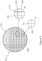
- Figure 2 (a) is a plan view of a wafer substrate 120.
- the wafer substrate 120 has a mask formed on its upper surface from a suitable material such aluminium.
- the mask defines a plurality of dicing lanes 122.
- Each dicing lane 122 corresponds to a linear gap in the mask which exposes the underlying material of the substrate to the plasma 22.
- a mask is deposited to define a plurality of dicing lanes substantially as shown in Figure 2 , namely a plurality of co-linear dicing lanes extending in one direction and a plurality of co-linear dicing lanes extending in an orthogonal direction. In this way, a cross hatch pattern of dicing lanes is obtained.
- Figures 2 (b) and 2 (c) show portions of the surface of the substrate wafer 120 in more detail. More particularly, Figure 2 (b) shows a region in which two co-linear dicing lanes intersect with two perpendicular dicing lanes. Figure 2 (c) shows the intersection of a single dicing lane with a perpendicular dicing lane.
- the infrared detector maybe configured and positioned to monitor the whole of the upper surface of the substrate wafer 120 or monitor just a portion of a substrate wafer 120. For example, the portion shown in Figure 2 (b) or the portion shown in Figure 2 (c) might be specifically monitored. Suitable optics might be employed so that the desired area can be monitored with the infrared detector.
- Figure 3 shows a cross section of a portion of a wafer substrate 130 during the course of a plasma dicing process.
- the substrate wafer 130 comprises the bulk substrate material 130a with the mask 130b formed thereon to define a dicing lane 130c.
- the wafer substrate 130 is mounted on a tape 132 which attaches the wafer substrate 130 to a frame (not shown).
- the 130 bulk substrate material 130a has a thin layer (up to 5 microns) of a backside metal on its rear surface.
- the backside metal could be mounted on the tape 132.
- an infrared detector 134 is also shown in Figure 3 to monitor infrared emission from the dicing lane 130c.
- the wafer substrate 130 is positioned in a suitable apparatus such as the apparatus shown in Figure 1 .
- the infrared detector 134 forms part of this apparatus.
- Figure 3 shows in semi-schematic form the appearance of the dicing lane 130c after a substantial portion of the plasma dicing process has been completed.
- the dicing lane 130c has been substantially etched to form a trench structure.
- the floor of the trench structure 136 corresponds to the etch front at this point in the process.
- t remaining thickness
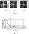
- FIG. 4 shows a pictorial sequence of the temperature distribution in the vicinity of a dicing lane. More particularly, the results shown in Figure 4 correspond generally to the portion of a substrate shown in Figure 2(c) where two mutually perpendicular dicing lanes intercept. A silicon substrate has been assumed for the purposes for the SEM model.
- Figure 4(a) shows the temperature distribution when a 10 micron thickness of silicon remains in the dicing lanes. It can be seen that a substantial amount of heat spreads into the adjacent dies.
- Figure 2 (b) shows the temperature distribution when a two micron thickness of silicon remains in the dicing lanes. It can be seen that heat transfer into the surrounding dies is far less efficient.
- Figure 4 (c) shows the temperature distribution when there is only a 200 nm layer of silicon remaining in the dicing lanes. It can be seen that heat transfer into the adjacent dies is minimal and instead the heat flux is concentrated in the dicing lanes. The intersection between mutually perpendicular dicing lanes gives rise to a particularly high heat flux.
- the FEM is based on a consistent heat load at the different etch depths. The rate of silicon etch and therefore the total heat load generated at the etch front is the same in all instances.
- Figures 4 and 5 show time averaged temperatures during the silicon etch. With a switched etch process, in which cyclic etch and deposition steps are used, the situation is even more complex as the heat load and etch front temperature follows the alternate etch and deposition cycle. This is show in Figure 6 which shows the time dependent temperature 160 at the rear of the silicon wafer directly below the etch front during a cyclic (Bosch) silicon etch process. The results are based on the FEM model described above with a periodic time-dependent heat load of arbitrary amplitude.
- the present inventors have realised that the final phase of a plasma dicing process, up to and including the singulation end point, can be sensitively detected by monitoring infrared emission from the dicing lanes.
- sensitive detection can be achieved against the background thermal emission occurring within a plasma dicing chamber from other energetic heat sources such as the plasma itself.
- a relatively simple and inexpensive device such as a pyrometer can be used for these purposes.
- an infrared camera can provide excellent results.
- the infrared detector monitors in real time the infrared emission from the dicing lanes.
- the average wafer temperature or the temperature in a specific region of the wafer or in a specific dicing lane can be monitored.
- the apparatus can monitor for a pre-set maximum temperature to be recorded anywhere in the field of view.
- the present inventors have realised that the significant rise in temperature in the dicing lanes as the etch front approaches the singulation point its indicative of the final phase of the plasma dicing process being entered. Additionally, this phenomenon enables the final phase to be detected with a good sensitivity by monitoring infrared emission from the dicing lanes. The signal from the infrared detector is fed back to the controller. Once a certain condition has been detected, the controller can switch the process to another mode. This trigger condition may be a certain thickness of material remaining in the lane to be etched.
- the controller can recognise how much material remains in the dicing lane to be etched from the signal produced by the infrared detector. For example, the controller can compare the output signal with a numerical model.
- the mode that the process is switched to may utilise less severe etch conditions to reduce the heat load. For example, a lower etch rate might be used. Alternatively, the etch may completely halted so that a small amount of material remains at the bottom of the dicing lanes.
- the temperature in the dicing lanes drops abruptly. This is because once the singulation is complete is there is little or no exothermic chemical reaction occurring, so the temperature of the wafer reduces.
- This can be used as a way of detecting the end point from the infrared emission from the dicing lanes. The detection of the end point can be used to trigger the end of the process. This represents an alternative end point detection method to optical emission based end point detection. It is advantageous to use infrared emission to directly detect the end point for reasons such as cost, simplicity, and a desirability of using the same hardware for end pointing and other process conditions.
- Figure 8 shows optical emission signals 182 and signals 180 obtained using a pyrometer. Good agreement is observed between the two sets of signals. In particular, both sets of signals indicate a singulation end point for two separate dicing processes at a time of approximately 250 seconds. The skilled reader will understand that after the end point is reached, many process run an 'over etch' step to clear a residual material from the etched features. However, the chemical energy realised in the over etch is a fraction of the realised in the main bulk etch. Accordingly, a discernible decrease in infrared emission is still to be expected once the end point is reached.
- the present invention can be used to predict the end point in advance of its actual occurrence.
- the end point prediction can be performed in addition to or instead of direct end point detection. This is an extremely advantageous facet of the present invention.
- the present invention enables the detection of certain conditions associated with the final phase of the plasma dicing process, such as the detection of a certain remaining thickness of material in the dicing lanes. From this, the time to the end point can be derived using suitable means, such as a numerical model, look up tables, or artificial intelligence.
- the prediction of the end point can be refined as the etch proceeds.
- process variables can be altered once a given condition has been detected, and any such alteration of process variables can be accounted for when predicting the end point.
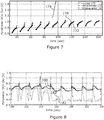
- Figure 7 shows pyrometer signal obtained during the etch steps of a switched (cyclic) etching deposition process.
- Pyrometer signal 170 (blue data) corresponds to instances of successful clamping of the wafer/tape/frame to a cooled electrostatic chuck.
- Pyrometer signal 170 corresponds to a partial declamping of the wafer/tape/frame from the electrostatic chuck.
- Pyrometer signal 174 corresponds to a full declamping of the wafer/tape/frame from the electrostatic chuck.
- the present invention can be used to detect the occurrence of thermal run away.
- the controller can abort the etching process and initiate appropriate recovery actions.
- Another fault can occur when there is a breakdown in the passivation layer on the sidewall of a dicing lane or when a stop layer at the feature base is breached. In these instances chemical heating will occur which can be detected by monitoring infrared emission. This can also be flagged by the controller as a processing fault.
- Thermal monitoring of the substrate wafer is possible in a plasma chamber as a large proportion of the signal comes from the infrared radiation emitted by the substrate. This means that the material and the surface of the substrate are less important than might have been expected.
- the data presented herein were obtained from wafers having an aluminium mask which covers approximately 75% of the surface area of the wafer.
- the cycles of the Bosch process etching are still clearly discernible using a pyrometer as an infrared detector.
- the surface material of the substrate and the viewing angle of the infrared detector do make a difference to the background layer of the signal due to reflections from the chamber walls. This can make it somewhat difficult to derive an absolute substrate temperature from the infrared emission.
- the absolute temperature is not required.
- the local temperature at the rear of the substrate underneath the dicing lanes increases as the etch front approaches the singulation point. This effect gets stronger as the lateral dimensions of the etch features increase.
- the temperature spike may be below the sensitivity level of a given infrared detector. This may be overcome by including a test structure in the substrate which is within the field of view of the infrared detector. In this way, a more easily detectable local temperature change can be provided.
- the invention is equally applicable to substrates that have one or more backside metal (BSM) layers attached thereto and substrates that do not.
- BSM backside metal
- the invention has been exemplified in relation to substrates carried on a tape and frame arrangement, this is not a limiting aspect of the invention. Instead, the invention can be applied to systems which do not use a tape and frame arrangement, such a systems in which the substrate is directly supported on a platen or other substrate support.
Landscapes
- Engineering & Computer Science (AREA)
- Physics & Mathematics (AREA)
- Manufacturing & Machinery (AREA)
- Power Engineering (AREA)
- Microelectronics & Electronic Packaging (AREA)
- Computer Hardware Design (AREA)
- Plasma & Fusion (AREA)
- Chemical & Material Sciences (AREA)
- General Physics & Mathematics (AREA)
- Condensed Matter Physics & Semiconductors (AREA)
- Analytical Chemistry (AREA)
- Spectroscopy & Molecular Physics (AREA)
- General Chemical & Material Sciences (AREA)
- Chemical Kinetics & Catalysis (AREA)
- Drying Of Semiconductors (AREA)
- Dicing (AREA)
Description
- This invention relates to a method of detecting a condition associated with a final phase of a plasma dicing process. The invention relates also to associated apparatus.
- Plasma dicing is a well known technique in which dies are singulated using a plasma etch process. Typically, the dies are formed from a semiconductor material such as silicon and are used in electronic applications. The process of plasma dicing can generate a significant amount of heat due to exothermic chemical reactions, ion bombardments and emission from the plasma. Additionally, it is usual to heat the plasma etch chamber to an elevated temperature, typically around 60 °C, to ensure that by-products are volatile. The volatile by-products can then be pumped away. In particular, in silicon etching using a fluorine based plasma, the enthalpy of formation of the reaction Si+4F→SiF4 is 1.615MJ/mol. This is extremely exothermic and results in a significant heat load.
- The dicing of other semiconductor substrates can have high associated thermal budgets as well. For example, the dicing of GaAs wafers using chlorine based plasma chemistry can have a high thermal budget due to the continuous RF power applied to the wafer during the dicing process. For a 150mm diameter wafer, this can be of the order of several hundred Watts. This heat load is in addition to the positive enthalpy of formation of gallium chloride (211kJ/mol) and arsenic chloride (123kJ/mol).
- Because of the high temperatures associated with the plasma dicing process, it is usual to cool the substrate. Typically, the substrate is clamped to a cooled platen using electrostatic or mechanical methods or combination of both methods. It is common to the mount the substrate on a frame using tape. The tape that is used for this purpose is typically formed from a polymeric material having one or more adhesive layers formed thereon. Care has to be taken to keep the polymeric mounting tape cool to avoid deformation or 'burning'. 'Burning' can occur when the tape is heated beyond its thermoplastic (glass) transition point, or when a chemical reaction occurs between the tape and active species in the plasma, or when the tape decomposes into constituent polymeric compounds. In the latter case some of the constituent polymeric compounds may change phase into liquid form. Additionally, the heat load can cause out-gassing, which creates a pocket of trapped gas underneath the tape which may appear as a blister and initiate the 'burning' state. Therefore, the damage caused by tape deformation and 'burning' can be quite substantial. Significant damage to both the front side and the back side of the taped frame can occur during the plasma dicing process. Furthermore, outgassing increases the pressure in the wafer backside, and this can cause the wafer to declamp. A declamped wafer loses thermal contact with the temperature controlled surface of the platen and overheats rapidly. This can cause the tape to melt. Declamping from the platen can be very difficult to detect using conventional methods such as helium coolant gas leakage or capacitative sensing. In the case of a thinned, possibly singulated wafer, with no mechanical stiffness, localised declamping is possible.
- It is known to monitor optical emission in order to determine the plasma dicing end point. It is also known to use the end point detection of the singulation breakthrough to automatically adjust the etching process to a less energetic etch rate or a 'soft landing' mode. However, this approach has a fundamental flaw. This is because the optical emission end point technique can only signal the singulation event itself. This too late in the process to properly prevent overheating of the tape, because the high temperatures that can cause the burning of the tape have already occurred earlier in the dicing process.
- One solution to this problem is to adjust the etch to a less energetic, lower etch rate or 'soft landing' mode prior to the end point. The point at which the adjustment is made is estimated, based on the nominal wafer thickness and expected etch rate. The lower etch rate is then used through to the singulation end point. The singulation can be optically detected and further automatic process adjustment can be applied as necessary. This approach is not particularly satisfactory because it based on estimates. In particular, this approach is less than ideal if the wafer thickness is not consistent. If the wafer thickness is not consistent, then the etch times will vary and this will result in the estimated point at which the 'soft landing' mode is activated being inaccurate. For example, for a typical dicing after grind (DAG) application, the bulk silicon etch rate will be of the order of 22 microns/min, the low etch rate will be around 16 microns/min and the 'soft landing' etch rate will be about 6 microns/min. For a 100 micron thick wafer set to etch at 22 microns/min to a target depth of 95 microns before switching to a etch rate of 6 microns/min, the plasma dicing process will take approximately 5.2 minutes. However, if the wafer-to-wafer thickness variation is 105±5 microns the thickest wafer will take 6.8 minutes to etch. If the point at which the soft landing mode is activated is set to ensure that the thinnest wafers can be treated satisfactorily, then it follows that the thickest wafer will be subject to an extended period of time during which a low etch rate is used. This is undesirable from a manufacturing perspective. In the back-end electronic packaging industry, there are many application types and wafers of many different thicknesses are processed. A system that can etch at a high rate until the end point is approached would be extremely desirable.
- Therefore there is a real need to detect when the plasma dicing process has entered its final phase, prior to the singulation breakthrough in a dicing lane. The process conditions could then be adjusted accordingly. Although the need is particularly acute with substrates mounted on taped frames, the need applies also to the processing of substrates that are not mounted on taped frames. There is a general desire to actually adjust process conditions in the final phase of the plasma dicing process in order to optimise heat management and other process considerations.
- Furthermore there is a need to detect the end point of the wafer dicing process without the need for an expensive optical emission spectrometer. It would be highly desirable to provide a way of predicting the end point instead of, or in addition to, directly detecting the end point when it occurs. This would enable certain desirable operations (such as those discussed above) to be performed in advance of the completion of the dicing process. However, at the present time, there is no available technique which uses empirical data to allow the end point as a plasma dicing end point to be predicted.
-
US 2015/162244 A1 andWO 2015/134111 A1 disclose plasma dicing processes that utilise an optical emission spectrometer to detect the end point of a wafer dicing process.US 6174407 B1 discloses an apparatus and method for detecting an end point of an etching process by transmitting infrared light signals through a semiconductor wafer. - The present invention, in at least some of its embodiments, addresses some or all of the above mentioned problems, needs and desires.
- According to a first aspect of the invention there is provided a method of detecting a condition associated with a final phase of a plasma dicing process comprising the steps of:
- providing a non-metallic substrate having a plurality of dicing lanes defined thereon;
- plasma etching through the substrate along the dicing lines, wherein during the plasma etching infrared emission emanating from at least a portion of the dicing lanes is monitored so that an increase in infrared emission from the dicing lanes is observed as the final phase of the plasma dicing operation is entered; and
- detecting the condition associated with the final phase of the plasma dicing from the monitored infrared emission.
- The present inventors have realised that infrared emission from the dicing lanes can be an excellent indicator that the end point of the plasma dicing process is approaching. It is surprising that infrared emission from the dicing lanes can act as an effective indicator of the final phase of the plasma dicing process. This is because, as explained earlier, there is a significant amount of heat generated during the plasma dicing process through sources such as the plasma itself and heat which is further applied to the plasma etch chamber to ensure the by-products are volatilised.
- At least one process variable may be altered in response to the detection of the condition. The process variable may be altered to adjust the plasma etching. For example, the plasma etching may be adjusted to reduce the rate of etching of the substrate. The skilled reader will appreciate that there are various process variable s which might be altered in order to achieve a desired adjustment of the plasma etching. For example, the rate of etching of the substrate might be reduced by adjusting the power coupled into the plasma. This may be a RF power or other suitable form of power that can drive a plasma. Other process variables, such as gas flows, might be adjusted as is known to the skilled reader.
- The process variable may be altered to control a temperature associated with the plasma dicing process. Typically, the process variable is altered to adjust the plasma etching. However, in principle, other process variables may be altered to control the temperature associated with the plasma dicing process. For example, the substrate may be disposed on a substrate support. The substrate support may be cooled. The process variable that is altered may be the cooling of the substrate support.
- The plasma etching may be stopped in response to the detection of the condition.
- The condition may be the approach of the end point.
- The condition may be the end point. The end point may be predicted in advance based on the observation of an increase in infrared emission from the dicing lanes. The end point may be predicted by comparison of the increase of infrared emission from the dicing lanes with a numerical model.
- Alternatively, the end point may be directly detected from the monitored infrared emission. In these embodiments, the increase in infrared emission from the dicing lanes observed as the final phase is entered may be followed by a decrease in infrared emission. The decrease in infrared emission may be directly indicative of the end point.
- The substrate may be attached to a frame with a tape. The frame may be disposed on a substrate support such as a platen. A process variable may be altered in response to the detection of the condition. In these embodiments, the process variable may be altered to control the temperature of the tape. The process variable may be altered to maintain the temperature of the tape below an upper limit. The upper limit may be set so as to avoid heat induced damage to the tape such as burning, blistering, or outgassing.
- The substrate may be disposed on a substrate support such as a platen without employing a frame and tape arrangement.
- The substrate may be a semiconductor substrate.
- The substrate may be silicon.
- The substrate may be GaAs, GaN, InP or SiC.
- Alternatively, the substrate may be a dielectric substrate. The substrate may be a glass or a substrate formed from an epoxy material.
- The plasma etching may be performed using a cyclic etch and deposition process. The cyclic etch and deposition process may be a process of the kind commonly known as the 'Bosch process', originally described in
US 5501893 . - Conveniently, the infrared emission may be monitored using a pyrometer. This is an extremely cost effective solution. Furthermore, it is possible to monitor the whole of the surface of the substrate or to monitor a portion of the surface of the substrate. A relatively small portion of the surface of the substrate (but greater than the area of an individual die) may be monitored which avoids a requirement for accurate alignment.
- Alternatively, an infrared camera may be used to monitor the infrared emission. The infrared camera may be a CCD array. This permits greater detail to be obtained. The whole surface of the wafer or a portion of the surface of the substrate may be monitored. It is also possible to provide improved information in relation to etch uniformity for the centre to the edge of the substrate.
- The condition may be a fault condition. The fault condition may be a loss of clamping of the substrate to a substrate support, a breakdown in a passivation layer or a breach in a stop layer at a base of the dicing lanes.
- The condition may be related to the uniformity of etching across the substrate. The condition may be related to the uniformity of etching from the edge to the centre of the substrate. In these embodiments, infrared emission from substantially the whole of the substrate may be monitored. Typically, the substrate has a mask formed thereon which defines the dicing lanes. The mask may be formed from any suitable material, such as aluminium.
- Surprisingly, the invention is equally applicable to substrates that have one or more backside metal (BSM) layers attached thereto and substrates that do not have a backside metallization. The detection of the condition associated with the final phase of the plasma dicing from the monitored infrared emission does not appear to be affected by the presence of a backside metallization. According to a second aspect of the invention there is provided a plasma dicing apparatus comprising:
- a chamber;
- a substrate support configured to support a non-metallic substrate of the kind having dicing lanes;
- a plasma generator configured to generate plasma in a chamber suitable to etch through the substrate along the dicing lanes;
- an infrared detector configured to monitor infrared emissions emanating from at least a portion of the dicing lanes; and
- a condition detector configured to detect a condition associated with a final phase of the plasma dicing process from the monitored infrared emission.
- The infrared detector may be a pyrometer or an infrared camera.
- The apparatus may further comprise a controller for altering at least one process variable in response to the detection of the condition. Typically the condition detector and the controller comprise a computer or other micro processor based device. The condition detector and the controller may be embodied within a single computer or other microprocessor based device. Whilst the invention is described above it extends to any inventive combination of the features set out above or in the following description, drawing or claims. For example, any feature described in relation to the first aspect of the invention is also disclosed in combination with the second aspect of the invention and visa versa. The skilled reader will understand that the condition detector and/ or the controller of the second aspect of the invention may be suitably configured to perform process steps described in relation to the first aspect of the invention.
- Embodiments of methods and apparatus in accordance with the invention will now be described with reference to the accompanying drawings, in which: -
-
Figure 1 shows an apparatus of the invention; -
Figure 2 is a plan view of a substrate wafer with dicing lanes; -
Figure 3 show the detection of the remaining of material in a dicing lane and includes a cross sectional view of a portion of a substrate; -
Figure 4 shows the temperature distribution in the vicinity of a dicing lane obtained from a FEM model as the etch front approaches singulation with (a) 10 microns of silicon remaining (b) 2 microns of silicon remaining and (c) 0.2 microns of silicon remaining; -
Figure 5 shows the temperature at the rear of a silicon wafer below a dicing lane as the etch front approaches obtained from a FEM model; -
Figure 6 shows temperature as a function of time at the rear of a silicon wafer below a dicing lane during a cyclic etch and deposition process obtained from a FEM model; -
Figure 7 show pyrometer signal during the etch step of a cyclic etch and deposition process; and -
Figure 8 shows pyrometer (solid) and optical omission (dashed) signals obtained during a plasma dicing process. -
Figure 1 shows a plasma dicing apparatus of the invention, depicted generally at 10. Theapparatus 10 comprises achamber 12 having awafer loading slot 14. The interior of thechamber 12 houses aplaten 16 on which a work piece such awafer 18 may be loaded. Theplaten 16 as shown inFigure 1 is in a raised position which is adopted during plasma dicing of the substrate. The platen can be moved between this raised position and a lower position. The lower position of the platen is adopted for receiving the substrate through the wafer loading slot. Thechamber 12 is surrounded by aninductive coil 20. Theinductive coil 20 is connected to a RF power generator (not shown) through an impedance matching network (not shown) as is well known in the art. Suitable etching gas or gases are supplied to thechamber 12 through a gas inlet system (not shown) and RF power is applied to thecoil 20 to produce aplasma 22 in thechamber 12. Gases are removed from the chamber using a suitable vacuum exhaust system. - The
apparatus 10 further comprises aninfrared detector 24 which is mounted so as to monitor infrared emission during the plasma dicing process from thesubstrate 18. Conveniently, theinfrared detector 24 can be mounted on or above the top of thechamber 12. However, in principle, the infrared detector can be mounted elsewhere provided that it is in a position suitable to monitor infrared emission from thesubstrate 18. In the embodiment shown inFigure 1 the infrared detector is mounted at one end of apassage way 26 formed in the top section of thechamber 12. Other ways of mounting the infrared detector might be contemplated, such as directly mounting theinfrared detector 24 on the top surface of thechamber 12. Theinfrared detector 24 can be in any suitable form, although it has been found that there are advantages associated with using a pyrometer or an infrared camera such as a CCD array. Theapparatus 10 further comprise acontroller 28. The controller receives the output of theinfrared detector 24 and processes the output in order to detect one or more conditions associated with the final phase of the plasma dicing process. The way in which thecontroller 28 operates to recognise the condition or conditions is described in more detail below. On recognition of a condition, the controller may act to adjust or otherwise control one or more operations of the apparatus. In particular, the plasma dicing process may be adjusted or halted once a condition associated with the final stage of the plasma dicing process has been detected. Thecontroller 28 may comprise or be connected to a suitable graphical user interface to display information associated with the plasma dicing process. This information can include an indication that the condition has been detected. -
Figure 2 (a) is a plan view of awafer substrate 120. Thewafer substrate 120 has a mask formed on its upper surface from a suitable material such aluminium. The mask defines a plurality of dicinglanes 122. Eachdicing lane 122 corresponds to a linear gap in the mask which exposes the underlying material of the substrate to theplasma 22. Typically, a mask is deposited to define a plurality of dicing lanes substantially as shown inFigure 2 , namely a plurality of co-linear dicing lanes extending in one direction and a plurality of co-linear dicing lanes extending in an orthogonal direction. In this way, a cross hatch pattern of dicing lanes is obtained.Figures 2 (b) and 2 (c) show portions of the surface of thesubstrate wafer 120 in more detail. More particularly,Figure 2 (b) shows a region in which two co-linear dicing lanes intersect with two perpendicular dicing lanes.Figure 2 (c) shows the intersection of a single dicing lane with a perpendicular dicing lane. The infrared detector maybe configured and positioned to monitor the whole of the upper surface of thesubstrate wafer 120 or monitor just a portion of asubstrate wafer 120. For example, the portion shown inFigure 2 (b) or the portion shown inFigure 2 (c) might be specifically monitored. Suitable optics might be employed so that the desired area can be monitored with the infrared detector. -
Figure 3 shows a cross section of a portion of awafer substrate 130 during the course of a plasma dicing process. Thesubstrate wafer 130 comprises thebulk substrate material 130a with themask 130b formed thereon to define adicing lane 130c. Thewafer substrate 130 is mounted on atape 132 which attaches thewafer substrate 130 to a frame (not shown). In some embodiments the 130bulk substrate material 130a has a thin layer (up to 5 microns) of a backside metal on its rear surface. The backside metal could be mounted on thetape 132. Also shown inFigure 3 is aninfrared detector 134. Theinfrared detector 134 is positioned to monitor infrared emission from thedicing lane 130c. Thewafer substrate 130 is positioned in a suitable apparatus such as the apparatus shown inFigure 1 . Theinfrared detector 134 forms part of this apparatus.Figure 3 shows in semi-schematic form the appearance of thedicing lane 130c after a substantial portion of the plasma dicing process has been completed. Thedicing lane 130c has been substantially etched to form a trench structure. The floor of thetrench structure 136 corresponds to the etch front at this point in the process. In the example shown inFigure 3 , a relatively small remaining thickness (t) of material remains to be etched in thedicing lane 130c. - A FEM (Finite Element Method) model has been built to examine the plasma dicing process in more detail when there is a relatively small remaining thickness (t) of substrate remaining to be etched in the dicing lanes.
Figure 4 shows a pictorial sequence of the temperature distribution in the vicinity of a dicing lane. More particularly, the results shown inFigure 4 correspond generally to the portion of a substrate shown inFigure 2(c) where two mutually perpendicular dicing lanes intercept. A silicon substrate has been assumed for the purposes for the SEM model.Figure 4(a) shows the temperature distribution when a 10 micron thickness of silicon remains in the dicing lanes. It can be seen that a substantial amount of heat spreads into the adjacent dies.Figure 2 (b) shows the temperature distribution when a two micron thickness of silicon remains in the dicing lanes. It can be seen that heat transfer into the surrounding dies is far less efficient.Figure 4 (c) shows the temperature distribution when there is only a 200 nm layer of silicon remaining in the dicing lanes. It can be seen that heat transfer into the adjacent dies is minimal and instead the heat flux is concentrated in the dicing lanes. The intersection between mutually perpendicular dicing lanes gives rise to a particularly high heat flux. The FEM is based on a consistent heat load at the different etch depths. The rate of silicon etch and therefore the total heat load generated at the etch front is the same in all instances. Without wishing to be bound by any particular theory or conjecture, it is believed that the results shown inFigure 4 can be readily explained. Silicon is a relatively good thermal conductor and inFigure 4(a) the heat generated during the plasma dicing process is spread quite efficiently into the adjacent dies. As the etch proceeds, the remaining thickness of silicon in the dicing lanes reduces. It is believed that this limits the effective conductivity of heat into the surrounding dies. In other words, the lateral heat conductivity of the remaining silicon diminishes as the remaining thickness of silicon reduces.Figure 5 shows the temperature at the rear of the silicon wafer as the etch front approaches the rear surface of the silicon wafer. The point of singulation is achieved when the etch front reaches the rear surface of the wafer. The same FEM model used to generate the results shown inFigure 4 is used to generate thetemperature curve 150 shown inFigure 5 . It is apparent that as the thickness of remaining silicon in the dicing lane approaches zero, the local temperature directly under the dicing lane increases substantially. The rate of temperature rise increases at around 1.5 microns of remaining silicon and increases substantially with around 500-600nm of silicon remaining. -
Figures 4 and 5 show time averaged temperatures during the silicon etch. With a switched etch process, in which cyclic etch and deposition steps are used, the situation is even more complex as the heat load and etch front temperature follows the alternate etch and deposition cycle. This is show inFigure 6 which shows the timedependent temperature 160 at the rear of the silicon wafer directly below the etch front during a cyclic (Bosch) silicon etch process. The results are based on the FEM model described above with a periodic time-dependent heat load of arbitrary amplitude. - The present inventors have realised that the final phase of a plasma dicing process, up to and including the singulation end point, can be sensitively detected by monitoring infrared emission from the dicing lanes. Surprisingly, sensitive detection can be achieved against the background thermal emission occurring within a plasma dicing chamber from other energetic heat sources such as the plasma itself. Even more surprisingly, a relatively simple and inexpensive device such as a pyrometer can be used for these purposes. Alternatively, an infrared camera can provide excellent results. The infrared detector monitors in real time the infrared emission from the dicing lanes. The average wafer temperature or the temperature in a specific region of the wafer or in a specific dicing lane can be monitored. Alternatively, the apparatus can monitor for a pre-set maximum temperature to be recorded anywhere in the field of view. The present inventors have realised that the significant rise in temperature in the dicing lanes as the etch front approaches the singulation point its indicative of the final phase of the plasma dicing process being entered. Additionally, this phenomenon enables the final phase to be detected with a good sensitivity by monitoring infrared emission from the dicing lanes. The signal from the infrared detector is fed back to the controller. Once a certain condition has been detected, the controller can switch the process to another mode. This trigger condition may be a certain thickness of material remaining in the lane to be etched. This is possible because the local temperature detected in the dicing lanes is a function of the material remaining in the lane and not the depth etched. Therefore, the controller can recognise how much material remains in the dicing lane to be etched from the signal produced by the infrared detector. For example, the controller can compare the output signal with a numerical model. The mode that the process is switched to may utilise less severe etch conditions to reduce the heat load. For example, a lower etch rate might be used. Alternatively, the etch may completely halted so that a small amount of material remains at the bottom of the dicing lanes.
- If the etch is allowed to proceed to the singulation point where the material in the dicing lanes is completely etched away, then the temperature in the dicing lanes drops abruptly. This is because once the singulation is complete is there is little or no exothermic chemical reaction occurring, so the temperature of the wafer reduces. This can be used as a way of detecting the end point from the infrared emission from the dicing lanes. The detection of the end point can be used to trigger the end of the process. This represents an alternative end point detection method to optical emission based end point detection. It is advantageous to use infrared emission to directly detect the end point for reasons such as cost, simplicity, and a desirability of using the same hardware for end pointing and other process conditions. Experiments have been performed using optical emission based end point detection and detection based on infrared emission from the dicing lane.
Figure 8 shows optical emission signals 182 and signals 180 obtained using a pyrometer. Good agreement is observed between the two sets of signals. In particular, both sets of signals indicate a singulation end point for two separate dicing processes at a time of approximately 250 seconds. The skilled reader will understand that after the end point is reached, many process run an 'over etch' step to clear a residual material from the etched features. However, the chemical energy realised in the over etch is a fraction of the realised in the main bulk etch. Accordingly, a discernible decrease in infrared emission is still to be expected once the end point is reached. - Moreover, the present invention can be used to predict the end point in advance of its actual occurrence. The end point prediction can be performed in addition to or instead of direct end point detection. This is an extremely advantageous facet of the present invention. The present invention enables the detection of certain conditions associated with the final phase of the plasma dicing process, such as the detection of a certain remaining thickness of material in the dicing lanes. From this, the time to the end point can be derived using suitable means, such as a numerical model, look up tables, or artificial intelligence. The prediction of the end point can be refined as the etch proceeds. As noted above, process variables can be altered once a given condition has been detected, and any such alteration of process variables can be accounted for when predicting the end point.
- Fault detection can also be accomplished.
Figure 7 shows pyrometer signal obtained during the etch steps of a switched (cyclic) etching deposition process. Pyrometer signal 170 (blue data) corresponds to instances of successful clamping of the wafer/tape/frame to a cooled electrostatic chuck.Pyrometer signal 170 corresponds to a partial declamping of the wafer/tape/frame from the electrostatic chuck.Pyrometer signal 174 corresponds to a full declamping of the wafer/tape/frame from the electrostatic chuck. With the instances of successful clamping the temperature rise during each individual etch in the cycle should actually drop with increasing temperature. The temperature increases with time as the etch progresses. When the wafer/tape/frame partially declamps, thermal contact is lost and a greater temperature rise occurs during an individual etch depth. In the case of full declamping, a substantial thermal run away occurs which is manifest in still larger temperature rises during individual etch steps. In this instance, there is serious risk of the tape completely melting. The present invention can be used to detect the occurrence of thermal run away. On detection of declamping and/or thermal run away the controller can abort the etching process and initiate appropriate recovery actions. Another fault can occur when there is a breakdown in the passivation layer on the sidewall of a dicing lane or when a stop layer at the feature base is breached. In these instances chemical heating will occur which can be detected by monitoring infrared emission. This can also be flagged by the controller as a processing fault. - Thermal monitoring of the substrate wafer is possible in a plasma chamber as a large proportion of the signal comes from the infrared radiation emitted by the substrate. This means that the material and the surface of the substrate are less important than might have been expected. For example, the data presented herein were obtained from wafers having an aluminium mask which covers approximately 75% of the surface area of the wafer. However, the cycles of the Bosch process etching are still clearly discernible using a pyrometer as an infrared detector. The surface material of the substrate and the viewing angle of the infrared detector do make a difference to the background layer of the signal due to reflections from the chamber walls. This can make it somewhat difficult to derive an absolute substrate temperature from the infrared emission. However, in many instances, such as fault, end point and uniformity detection, the absolute temperature is not required.
- Numerous modifications to the methods and apparatus described above are possible. For example, as described above, the local temperature at the rear of the substrate underneath the dicing lanes increases as the etch front approaches the singulation point. This effect gets stronger as the lateral dimensions of the etch features increase. For very narrow dicing lanes, it is possible that the temperature spike may be below the sensitivity level of a given infrared detector. This may be overcome by including a test structure in the substrate which is within the field of view of the infrared detector. In this way, a more easily detectable local temperature change can be provided. The invention is equally applicable to substrates that have one or more backside metal (BSM) layers attached thereto and substrates that do not. Although the invention has been exemplified in relation to substrates carried on a tape and frame arrangement, this is not a limiting aspect of the invention. Instead, the invention can be applied to systems which do not use a tape and frame arrangement, such a systems in which the substrate is directly supported on a platen or other substrate support.
Claims (15)
- A method of detecting a condition associated with a final phase of a plasma dicing process comprising the steps of:providing a non-metallic substrate (18, 120) having a plurality of dicing lanes (122) defined thereon;plasma etching through the substrate (18, 120) along the dicing lanes (122), wherein during the plasma etching infrared emission emanating from at least a portion of the dicing lanes (122) is monitoredso that an increase in infrared emission from the dicing lanes (122) is observed as the final phaseof the plasma dicing operation is entered; anddetecting the condition associated with the final phase of the plasma dicing from the monitored infrared emission.
- A method according to claim 1 in which at least one process variable is altered in response to the detection of the condition.
- A method according to claim 2 in which the process variable is altered to adjust the plasma etching.
- A method according to claim 3 in which the plasma etching is adjusted to reduce the rate of etching of the substrate.
- A method according to any one of claims 2 to 4 in which the process variable is altered to control a temperature associated with the plasma dicing process.
- A method according to claim 2 in which the plasma etching is stopped in response to the detection of the condition.
- A method according to any previous claim in which the condition is the approach of the end point.
- A method according to any one of claims 1 to 6 in which the condition is the end point.
- A method according to any one of claims 1 to 6 in which the end point is predicted in advance based on the observation of an increase in infrared emission from the dicing lanes.
- A method according to claim 9 in which the end point is predicted by comparison to the increase of infrared emission from the dicing lanes with a numerical model or the end point is directly detected from the monitored infrared emission.
- A method according to claim 10 in which the increase in infrared emission from the dicing lanes observed as the final phase is entered is followed by a decrease in infrared emission which is directly indicative of the end point.
- A method according to any previous claim in which the substrate is attached to a frame with a tape.
- A method according to claim 12 when dependent on claim 5 in which the process variable is altered to control the temperature of the tape.
- A method according to any previous claim in which the substrate is a semiconductor substrate, preferably silicon, GaAs, GaN, InP or SiC.
- A plasma dicing apparatus (10) comprising:a chamber (12);a substrate support (16) configured to support a non-metallic substrate (18, 120) of the kind having dicing lanes (122);a plasma generator (20) configured to generate a plasma (22) in the chamber suitable to plasma etch through the substrate along the dicing lanes;an infrared detector (24) configured to monitor infrared emission emanating from at least a portion of the dicing lane; anda condition detector (28) configured to detect a condition associated with a final phase of the plasma dicing process from the monitored infrared emission.
Applications Claiming Priority (1)
| Application Number | Priority Date | Filing Date | Title |
|---|---|---|---|
| GBGB1611652.7A GB201611652D0 (en) | 2016-07-04 | 2016-07-04 | Method of detecting a condition |
Publications (2)
| Publication Number | Publication Date |
|---|---|
| EP3267465A1 EP3267465A1 (en) | 2018-01-10 |
| EP3267465B1 true EP3267465B1 (en) | 2019-11-27 |
Family
ID=56891252
Family Applications (1)
| Application Number | Title | Priority Date | Filing Date |
|---|---|---|---|
| EP17179411.8A Active EP3267465B1 (en) | 2016-07-04 | 2017-07-03 | Method and apparatus of detecting a condition in a plasma dicing process |
Country Status (7)
| Country | Link |
|---|---|
| US (1) | US10366899B2 (en) |
| EP (1) | EP3267465B1 (en) |
| JP (1) | JP6837395B2 (en) |
| KR (1) | KR102165795B1 (en) |
| CN (1) | CN107579044B (en) |
| GB (1) | GB201611652D0 (en) |
| TW (1) | TWI713757B (en) |
Families Citing this family (4)
| Publication number | Priority date | Publication date | Assignee | Title |
|---|---|---|---|---|
| CN105719965A (en) * | 2014-12-04 | 2016-06-29 | 北京北方微电子基地设备工艺研究中心有限责任公司 | Method and device for etching silicon dioxide substrate |
| US10636686B2 (en) | 2018-02-27 | 2020-04-28 | Lam Research Corporation | Method monitoring chamber drift |
| JP2020072141A (en) * | 2018-10-30 | 2020-05-07 | 株式会社ディスコ | Plasma etching device and processing method of wafer |
| CN110729186A (en) * | 2019-10-24 | 2020-01-24 | 东莞记忆存储科技有限公司 | Processing method for wafer cutting and separating |
Family Cites Families (23)
| Publication number | Priority date | Publication date | Assignee | Title |
|---|---|---|---|---|
| CA1071579A (en) * | 1976-09-13 | 1980-02-12 | Northern Telecom Limited | End point control in plasma etching |
| JPS62190728A (en) | 1986-02-18 | 1987-08-20 | Nippon Telegr & Teleph Corp <Ntt> | Method and apparatus for monitoring etching end point |
| JPH04206927A (en) | 1990-11-30 | 1992-07-28 | Tokuda Seisakusho Ltd | Etching apparatus |
| US5200023A (en) * | 1991-08-30 | 1993-04-06 | International Business Machines Corp. | Infrared thermographic method and apparatus for etch process monitoring and control |
| DE4241045C1 (en) | 1992-12-05 | 1994-05-26 | Bosch Gmbh Robert | Process for anisotropic etching of silicon |
| US6174407B1 (en) * | 1998-12-03 | 2001-01-16 | Lsi Logic Corporation | Apparatus and method for detecting an endpoint of an etching process by transmitting infrared light signals through a semiconductor wafer |
| US7053994B2 (en) * | 2003-10-28 | 2006-05-30 | Lam Research Corporation | Method and apparatus for etch endpoint detection |
| US7507638B2 (en) * | 2004-06-30 | 2009-03-24 | Freescale Semiconductor, Inc. | Ultra-thin die and method of fabricating same |
| US7560007B2 (en) * | 2006-09-11 | 2009-07-14 | Lam Research Corporation | In-situ wafer temperature measurement and control |
| US7946759B2 (en) * | 2007-02-16 | 2011-05-24 | Applied Materials, Inc. | Substrate temperature measurement by infrared transmission |
| CN100475414C (en) * | 2007-06-29 | 2009-04-08 | 华中科技大学 | Real time monitoring device of the three-dimensional laser beam welding and incising process |
| CN101419996B (en) * | 2008-12-04 | 2010-09-22 | 中国电子科技集团公司第十三研究所 | Infrared-ultraviolet multi-color detector and production process thereof |
| US8802545B2 (en) * | 2011-03-14 | 2014-08-12 | Plasma-Therm Llc | Method and apparatus for plasma dicing a semi-conductor wafer |
| US8912077B2 (en) * | 2011-06-15 | 2014-12-16 | Applied Materials, Inc. | Hybrid laser and plasma etch wafer dicing using substrate carrier |
| US8557682B2 (en) * | 2011-06-15 | 2013-10-15 | Applied Materials, Inc. | Multi-layer mask for substrate dicing by laser and plasma etch |
| CN104285500B (en) * | 2012-05-08 | 2017-11-28 | Ams传感器英国有限公司 | RF transmitter and NDIR sensors |
| EP3022638B1 (en) | 2013-07-18 | 2018-04-04 | Fasetto, L.L.C. | System and method for multi-angle videos |
| US9299614B2 (en) * | 2013-12-10 | 2016-03-29 | Applied Materials, Inc. | Method and carrier for dicing a wafer |
| KR101906695B1 (en) | 2014-03-07 | 2018-10-10 | 플라즈마-썸, 엘엘씨 | Method and apparatus for plasma dicing a semi-conductor wafer |
| JP6101227B2 (en) * | 2014-03-17 | 2017-03-22 | 株式会社東芝 | Plasma dicing method and plasma dicing apparatus |
| US9034771B1 (en) * | 2014-05-23 | 2015-05-19 | Applied Materials, Inc. | Cooling pedestal for dicing tape thermal management during plasma dicing |
| US10153204B2 (en) * | 2014-06-04 | 2018-12-11 | Flir Systems, Inc. | Wafer level packaging of reduced-height infrared detectors |
| SG10201903242QA (en) | 2014-10-13 | 2019-05-30 | Utac Headquarters Pte Ltd | Methods for singulating semiconductor wafer |
-
2016
- 2016-07-04 GB GBGB1611652.7A patent/GB201611652D0/en not_active Ceased
-
2017
- 2017-06-19 US US15/626,250 patent/US10366899B2/en active Active
- 2017-06-26 KR KR1020170080623A patent/KR102165795B1/en active IP Right Grant
- 2017-06-28 TW TW106121590A patent/TWI713757B/en active
- 2017-07-03 CN CN201710534660.1A patent/CN107579044B/en active Active
- 2017-07-03 JP JP2017130351A patent/JP6837395B2/en active Active
- 2017-07-03 EP EP17179411.8A patent/EP3267465B1/en active Active
Non-Patent Citations (1)
| Title |
|---|
| None * |
Also Published As
| Publication number | Publication date |
|---|---|
| CN107579044A (en) | 2018-01-12 |
| EP3267465A1 (en) | 2018-01-10 |
| KR102165795B1 (en) | 2020-10-14 |
| CN107579044B (en) | 2022-12-27 |
| GB201611652D0 (en) | 2016-08-17 |
| US20180005837A1 (en) | 2018-01-04 |
| TWI713757B (en) | 2020-12-21 |
| KR20180004663A (en) | 2018-01-12 |
| JP2018006758A (en) | 2018-01-11 |
| US10366899B2 (en) | 2019-07-30 |
| JP6837395B2 (en) | 2021-03-03 |
| TW201812831A (en) | 2018-04-01 |
Similar Documents
| Publication | Publication Date | Title |
|---|---|---|
| EP3267465B1 (en) | Method and apparatus of detecting a condition in a plasma dicing process | |
| TWI614854B (en) | Focusing ring temperature adjusting device and method | |
| EP3039715B1 (en) | Method for plasma dicing a semi-conductor wafer | |
| US9601437B2 (en) | Plasma etching and stealth dicing laser process | |
| TWI708306B (en) | Apparatus for plasma dicing | |
| JP7250076B2 (en) | Systems and methods for thermal management of bolted wafer chucks for wafer processing systems | |
| KR20150109459A (en) | Laser and plasma etch wafer dicing with etch chamber shield ring for film frame wafer applications | |
| EP2973668A1 (en) | Method and apparatus for plasma dicing a semi-conductor wafer | |
| EP3594998B1 (en) | Method for plasma dicing a semi-conductor wafer | |
| US9293304B2 (en) | Plasma thermal shield for heat dissipation in plasma chamber | |
| WO2006130573A2 (en) | Optimizing the thermal budget during a pulsed heating process | |
| KR20140138962A (en) | Platen clamping surface monitoring | |
| CN114520172A (en) | Wafer placement state detection method, semiconductor process chamber and equipment | |
| Barnett | Plasma Dicing 300mm Framed Wafers—Analysis of Improvement in Die Strength and Cost Benefits for Thin Die Singulation | |
| US9478455B1 (en) | Thermal pyrolytic graphite shadow ring assembly for heat dissipation in plasma chamber | |
| Barnett et al. | Considerations and benefits of plasma etch based wafer dicing | |
| US11545394B2 (en) | Semiconductor wafer dicing process | |
| KR200228632Y1 (en) | Temperature controlling system for the surface of an electrostatic chuck using heaters | |
| JPH04333228A (en) | Dry-etching device |
Legal Events
| Date | Code | Title | Description |
|---|---|---|---|
| PUAI | Public reference made under article 153(3) epc to a published international application that has entered the european phase |
Free format text: ORIGINAL CODE: 0009012 |
|
| STAA | Information on the status of an ep patent application or granted ep patent |
Free format text: STATUS: REQUEST FOR EXAMINATION WAS MADE |
|
| 17P | Request for examination filed |
Effective date: 20171130 |
|
| AK | Designated contracting states |
Kind code of ref document: A1 Designated state(s): AL AT BE BG CH CY CZ DE DK EE ES FI FR GB GR HR HU IE IS IT LI LT LU LV MC MK MT NL NO PL PT RO RS SE SI SK SM TR |
|
| AX | Request for extension of the european patent |
Extension state: BA ME |
|
| GRAP | Despatch of communication of intention to grant a patent |
Free format text: ORIGINAL CODE: EPIDOSNIGR1 |
|
| STAA | Information on the status of an ep patent application or granted ep patent |
Free format text: STATUS: GRANT OF PATENT IS INTENDED |
|
| INTG | Intention to grant announced |
Effective date: 20190712 |
|
| GRAS | Grant fee paid |
Free format text: ORIGINAL CODE: EPIDOSNIGR3 |
|
| GRAA | (expected) grant |
Free format text: ORIGINAL CODE: 0009210 |
|
| STAA | Information on the status of an ep patent application or granted ep patent |
Free format text: STATUS: THE PATENT HAS BEEN GRANTED |
|
| AK | Designated contracting states |
Kind code of ref document: B1 Designated state(s): AL AT BE BG CH CY CZ DE DK EE ES FI FR GB GR HR HU IE IS IT LI LT LU LV MC MK MT NL NO PL PT RO RS SE SI SK SM TR |
|
| REG | Reference to a national code |
Ref country code: GB Ref legal event code: FG4D |
|
| REG | Reference to a national code |
Ref country code: CH Ref legal event code: EP |
|
| REG | Reference to a national code |
Ref country code: AT Ref legal event code: REF Ref document number: 1207653 Country of ref document: AT Kind code of ref document: T Effective date: 20191215 |
|
| REG | Reference to a national code |
Ref country code: DE Ref legal event code: R096 Ref document number: 602017009047 Country of ref document: DE |
|
| REG | Reference to a national code |
Ref country code: IE Ref legal event code: FG4D |
|
| REG | Reference to a national code |
Ref country code: NL Ref legal event code: MP Effective date: 20191127 |
|
| REG | Reference to a national code |
Ref country code: LT Ref legal event code: MG4D |
|
| PG25 | Lapsed in a contracting state [announced via postgrant information from national office to epo] |
Ref country code: LT Free format text: LAPSE BECAUSE OF FAILURE TO SUBMIT A TRANSLATION OF THE DESCRIPTION OR TO PAY THE FEE WITHIN THE PRESCRIBED TIME-LIMIT Effective date: 20191127 Ref country code: FI Free format text: LAPSE BECAUSE OF FAILURE TO SUBMIT A TRANSLATION OF THE DESCRIPTION OR TO PAY THE FEE WITHIN THE PRESCRIBED TIME-LIMIT Effective date: 20191127 Ref country code: BG Free format text: LAPSE BECAUSE OF FAILURE TO SUBMIT A TRANSLATION OF THE DESCRIPTION OR TO PAY THE FEE WITHIN THE PRESCRIBED TIME-LIMIT Effective date: 20200227 Ref country code: NO Free format text: LAPSE BECAUSE OF FAILURE TO SUBMIT A TRANSLATION OF THE DESCRIPTION OR TO PAY THE FEE WITHIN THE PRESCRIBED TIME-LIMIT Effective date: 20200227 Ref country code: GR Free format text: LAPSE BECAUSE OF FAILURE TO SUBMIT A TRANSLATION OF THE DESCRIPTION OR TO PAY THE FEE WITHIN THE PRESCRIBED TIME-LIMIT Effective date: 20200228 Ref country code: LV Free format text: LAPSE BECAUSE OF FAILURE TO SUBMIT A TRANSLATION OF THE DESCRIPTION OR TO PAY THE FEE WITHIN THE PRESCRIBED TIME-LIMIT Effective date: 20191127 Ref country code: SE Free format text: LAPSE BECAUSE OF FAILURE TO SUBMIT A TRANSLATION OF THE DESCRIPTION OR TO PAY THE FEE WITHIN THE PRESCRIBED TIME-LIMIT Effective date: 20191127 Ref country code: NL Free format text: LAPSE BECAUSE OF FAILURE TO SUBMIT A TRANSLATION OF THE DESCRIPTION OR TO PAY THE FEE WITHIN THE PRESCRIBED TIME-LIMIT Effective date: 20191127 |
|
| PG25 | Lapsed in a contracting state [announced via postgrant information from national office to epo] |
Ref country code: IS Free format text: LAPSE BECAUSE OF FAILURE TO SUBMIT A TRANSLATION OF THE DESCRIPTION OR TO PAY THE FEE WITHIN THE PRESCRIBED TIME-LIMIT Effective date: 20200327 Ref country code: HR Free format text: LAPSE BECAUSE OF FAILURE TO SUBMIT A TRANSLATION OF THE DESCRIPTION OR TO PAY THE FEE WITHIN THE PRESCRIBED TIME-LIMIT Effective date: 20191127 Ref country code: RS Free format text: LAPSE BECAUSE OF FAILURE TO SUBMIT A TRANSLATION OF THE DESCRIPTION OR TO PAY THE FEE WITHIN THE PRESCRIBED TIME-LIMIT Effective date: 20191127 |
|
| PG25 | Lapsed in a contracting state [announced via postgrant information from national office to epo] |
Ref country code: AL Free format text: LAPSE BECAUSE OF FAILURE TO SUBMIT A TRANSLATION OF THE DESCRIPTION OR TO PAY THE FEE WITHIN THE PRESCRIBED TIME-LIMIT Effective date: 20191127 |
|
| PG25 | Lapsed in a contracting state [announced via postgrant information from national office to epo] |
Ref country code: EE Free format text: LAPSE BECAUSE OF FAILURE TO SUBMIT A TRANSLATION OF THE DESCRIPTION OR TO PAY THE FEE WITHIN THE PRESCRIBED TIME-LIMIT Effective date: 20191127 Ref country code: PT Free format text: LAPSE BECAUSE OF FAILURE TO SUBMIT A TRANSLATION OF THE DESCRIPTION OR TO PAY THE FEE WITHIN THE PRESCRIBED TIME-LIMIT Effective date: 20200419 Ref country code: DK Free format text: LAPSE BECAUSE OF FAILURE TO SUBMIT A TRANSLATION OF THE DESCRIPTION OR TO PAY THE FEE WITHIN THE PRESCRIBED TIME-LIMIT Effective date: 20191127 Ref country code: CZ Free format text: LAPSE BECAUSE OF FAILURE TO SUBMIT A TRANSLATION OF THE DESCRIPTION OR TO PAY THE FEE WITHIN THE PRESCRIBED TIME-LIMIT Effective date: 20191127 Ref country code: RO Free format text: LAPSE BECAUSE OF FAILURE TO SUBMIT A TRANSLATION OF THE DESCRIPTION OR TO PAY THE FEE WITHIN THE PRESCRIBED TIME-LIMIT Effective date: 20191127 Ref country code: ES Free format text: LAPSE BECAUSE OF FAILURE TO SUBMIT A TRANSLATION OF THE DESCRIPTION OR TO PAY THE FEE WITHIN THE PRESCRIBED TIME-LIMIT Effective date: 20191127 |
|
| REG | Reference to a national code |
Ref country code: DE Ref legal event code: R097 Ref document number: 602017009047 Country of ref document: DE |
|
| PG25 | Lapsed in a contracting state [announced via postgrant information from national office to epo] |
Ref country code: SM Free format text: LAPSE BECAUSE OF FAILURE TO SUBMIT A TRANSLATION OF THE DESCRIPTION OR TO PAY THE FEE WITHIN THE PRESCRIBED TIME-LIMIT Effective date: 20191127 Ref country code: SK Free format text: LAPSE BECAUSE OF FAILURE TO SUBMIT A TRANSLATION OF THE DESCRIPTION OR TO PAY THE FEE WITHIN THE PRESCRIBED TIME-LIMIT Effective date: 20191127 |
|
| REG | Reference to a national code |
Ref country code: AT Ref legal event code: MK05 Ref document number: 1207653 Country of ref document: AT Kind code of ref document: T Effective date: 20191127 |
|
| PLBE | No opposition filed within time limit |
Free format text: ORIGINAL CODE: 0009261 |
|
| STAA | Information on the status of an ep patent application or granted ep patent |
Free format text: STATUS: NO OPPOSITION FILED WITHIN TIME LIMIT |
|
| 26N | No opposition filed |
Effective date: 20200828 |
|
| PG25 | Lapsed in a contracting state [announced via postgrant information from national office to epo] |
Ref country code: AT Free format text: LAPSE BECAUSE OF FAILURE TO SUBMIT A TRANSLATION OF THE DESCRIPTION OR TO PAY THE FEE WITHIN THE PRESCRIBED TIME-LIMIT Effective date: 20191127 Ref country code: PL Free format text: LAPSE BECAUSE OF FAILURE TO SUBMIT A TRANSLATION OF THE DESCRIPTION OR TO PAY THE FEE WITHIN THE PRESCRIBED TIME-LIMIT Effective date: 20191127 Ref country code: SI Free format text: LAPSE BECAUSE OF FAILURE TO SUBMIT A TRANSLATION OF THE DESCRIPTION OR TO PAY THE FEE WITHIN THE PRESCRIBED TIME-LIMIT Effective date: 20191127 |
|
| PG25 | Lapsed in a contracting state [announced via postgrant information from national office to epo] |
Ref country code: IT Free format text: LAPSE BECAUSE OF FAILURE TO SUBMIT A TRANSLATION OF THE DESCRIPTION OR TO PAY THE FEE WITHIN THE PRESCRIBED TIME-LIMIT Effective date: 20191127 |
|
| PG25 | Lapsed in a contracting state [announced via postgrant information from national office to epo] |
Ref country code: MC Free format text: LAPSE BECAUSE OF FAILURE TO SUBMIT A TRANSLATION OF THE DESCRIPTION OR TO PAY THE FEE WITHIN THE PRESCRIBED TIME-LIMIT Effective date: 20191127 |
|
| REG | Reference to a national code |
Ref country code: CH Ref legal event code: PL |
|
| REG | Reference to a national code |
Ref country code: BE Ref legal event code: MM Effective date: 20200731 |
|
| PG25 | Lapsed in a contracting state [announced via postgrant information from national office to epo] |
Ref country code: IE Free format text: LAPSE BECAUSE OF NON-PAYMENT OF DUE FEES Effective date: 20200703 Ref country code: CH Free format text: LAPSE BECAUSE OF NON-PAYMENT OF DUE FEES Effective date: 20200731 Ref country code: LU Free format text: LAPSE BECAUSE OF NON-PAYMENT OF DUE FEES Effective date: 20200703 Ref country code: LI Free format text: LAPSE BECAUSE OF NON-PAYMENT OF DUE FEES Effective date: 20200731 |
|
| PG25 | Lapsed in a contracting state [announced via postgrant information from national office to epo] |
Ref country code: BE Free format text: LAPSE BECAUSE OF NON-PAYMENT OF DUE FEES Effective date: 20200731 |
|
| PG25 | Lapsed in a contracting state [announced via postgrant information from national office to epo] |
Ref country code: TR Free format text: LAPSE BECAUSE OF FAILURE TO SUBMIT A TRANSLATION OF THE DESCRIPTION OR TO PAY THE FEE WITHIN THE PRESCRIBED TIME-LIMIT Effective date: 20191127 Ref country code: MT Free format text: LAPSE BECAUSE OF FAILURE TO SUBMIT A TRANSLATION OF THE DESCRIPTION OR TO PAY THE FEE WITHIN THE PRESCRIBED TIME-LIMIT Effective date: 20191127 Ref country code: CY Free format text: LAPSE BECAUSE OF FAILURE TO SUBMIT A TRANSLATION OF THE DESCRIPTION OR TO PAY THE FEE WITHIN THE PRESCRIBED TIME-LIMIT Effective date: 20191127 |
|
| PG25 | Lapsed in a contracting state [announced via postgrant information from national office to epo] |
Ref country code: MK Free format text: LAPSE BECAUSE OF FAILURE TO SUBMIT A TRANSLATION OF THE DESCRIPTION OR TO PAY THE FEE WITHIN THE PRESCRIBED TIME-LIMIT Effective date: 20191127 |
|
| P01 | Opt-out of the competence of the unified patent court (upc) registered |
Effective date: 20230525 |
|
| PGFP | Annual fee paid to national office [announced via postgrant information from national office to epo] |
Ref country code: GB Payment date: 20230727 Year of fee payment: 7 |
|
| REG | Reference to a national code |
Ref country code: DE Ref legal event code: R082 Ref document number: 602017009047 Country of ref document: DE Representative=s name: KANDLBINDER, MARKUS, DIPL.-PHYS., DE |
|
| PGFP | Annual fee paid to national office [announced via postgrant information from national office to epo] |
Ref country code: FR Payment date: 20230725 Year of fee payment: 7 Ref country code: DE Payment date: 20230727 Year of fee payment: 7 |