EP3267426A1 - Display device and manufacturing method thereof - Google Patents
Display device and manufacturing method thereof Download PDFInfo
- Publication number
- EP3267426A1 EP3267426A1 EP15834662.7A EP15834662A EP3267426A1 EP 3267426 A1 EP3267426 A1 EP 3267426A1 EP 15834662 A EP15834662 A EP 15834662A EP 3267426 A1 EP3267426 A1 EP 3267426A1
- Authority
- EP
- European Patent Office
- Prior art keywords
- deformation
- display device
- substrate
- layer
- axis direction
- Prior art date
- Legal status (The legal status is an assumption and is not a legal conclusion. Google has not performed a legal analysis and makes no representation as to the accuracy of the status listed.)
- Granted
Links
Images



Classifications
-
- G—PHYSICS
- G06—COMPUTING OR CALCULATING; COUNTING
- G06F—ELECTRIC DIGITAL DATA PROCESSING
- G06F3/00—Input arrangements for transferring data to be processed into a form capable of being handled by the computer; Output arrangements for transferring data from processing unit to output unit, e.g. interface arrangements
- G06F3/01—Input arrangements or combined input and output arrangements for interaction between user and computer
- G06F3/011—Arrangements for interaction with the human body, e.g. for user immersion in virtual reality
-
- G—PHYSICS
- G09—EDUCATION; CRYPTOGRAPHY; DISPLAY; ADVERTISING; SEALS
- G09F—DISPLAYING; ADVERTISING; SIGNS; LABELS OR NAME-PLATES; SEALS
- G09F9/00—Indicating arrangements for variable information in which the information is built-up on a support by selection or combination of individual elements
-
- G—PHYSICS
- G06—COMPUTING OR CALCULATING; COUNTING
- G06F—ELECTRIC DIGITAL DATA PROCESSING
- G06F1/00—Details not covered by groups G06F3/00 - G06F13/00 and G06F21/00
- G06F1/16—Constructional details or arrangements
- G06F1/1601—Constructional details related to the housing of computer displays, e.g. of CRT monitors, of flat displays
-
- G—PHYSICS
- G02—OPTICS
- G02F—OPTICAL DEVICES OR ARRANGEMENTS FOR THE CONTROL OF LIGHT BY MODIFICATION OF THE OPTICAL PROPERTIES OF THE MEDIA OF THE ELEMENTS INVOLVED THEREIN; NON-LINEAR OPTICS; FREQUENCY-CHANGING OF LIGHT; OPTICAL LOGIC ELEMENTS; OPTICAL ANALOGUE/DIGITAL CONVERTERS
- G02F1/00—Devices or arrangements for the control of the intensity, colour, phase, polarisation or direction of light arriving from an independent light source, e.g. switching, gating or modulating; Non-linear optics
- G02F1/01—Devices or arrangements for the control of the intensity, colour, phase, polarisation or direction of light arriving from an independent light source, e.g. switching, gating or modulating; Non-linear optics for the control of the intensity, phase, polarisation or colour
- G02F1/13—Devices or arrangements for the control of the intensity, colour, phase, polarisation or direction of light arriving from an independent light source, e.g. switching, gating or modulating; Non-linear optics for the control of the intensity, phase, polarisation or colour based on liquid crystals, e.g. single liquid crystal display cells
- G02F1/133—Constructional arrangements; Operation of liquid crystal cells; Circuit arrangements
- G02F1/1333—Constructional arrangements; Manufacturing methods
-
- G—PHYSICS
- G09—EDUCATION; CRYPTOGRAPHY; DISPLAY; ADVERTISING; SEALS
- G09G—ARRANGEMENTS OR CIRCUITS FOR CONTROL OF INDICATING DEVICES USING STATIC MEANS TO PRESENT VARIABLE INFORMATION
- G09G3/00—Control arrangements or circuits, of interest only in connection with visual indicators other than cathode-ray tubes
- G09G3/20—Control arrangements or circuits, of interest only in connection with visual indicators other than cathode-ray tubes for presentation of an assembly of a number of characters, e.g. a page, by composing the assembly by combination of individual elements arranged in a matrix no fixed position being assigned to or needed to be assigned to the individual characters or partial characters
-
- G—PHYSICS
- G09—EDUCATION; CRYPTOGRAPHY; DISPLAY; ADVERTISING; SEALS
- G09G—ARRANGEMENTS OR CIRCUITS FOR CONTROL OF INDICATING DEVICES USING STATIC MEANS TO PRESENT VARIABLE INFORMATION
- G09G3/00—Control arrangements or circuits, of interest only in connection with visual indicators other than cathode-ray tubes
- G09G3/20—Control arrangements or circuits, of interest only in connection with visual indicators other than cathode-ray tubes for presentation of an assembly of a number of characters, e.g. a page, by composing the assembly by combination of individual elements arranged in a matrix no fixed position being assigned to or needed to be assigned to the individual characters or partial characters
- G09G3/2092—Details of a display terminals using a flat panel, the details relating to the control arrangement of the display terminal and to the interfaces thereto
-
- G—PHYSICS
- G02—OPTICS
- G02F—OPTICAL DEVICES OR ARRANGEMENTS FOR THE CONTROL OF LIGHT BY MODIFICATION OF THE OPTICAL PROPERTIES OF THE MEDIA OF THE ELEMENTS INVOLVED THEREIN; NON-LINEAR OPTICS; FREQUENCY-CHANGING OF LIGHT; OPTICAL LOGIC ELEMENTS; OPTICAL ANALOGUE/DIGITAL CONVERTERS
- G02F1/00—Devices or arrangements for the control of the intensity, colour, phase, polarisation or direction of light arriving from an independent light source, e.g. switching, gating or modulating; Non-linear optics
- G02F1/01—Devices or arrangements for the control of the intensity, colour, phase, polarisation or direction of light arriving from an independent light source, e.g. switching, gating or modulating; Non-linear optics for the control of the intensity, phase, polarisation or colour
- G02F1/13—Devices or arrangements for the control of the intensity, colour, phase, polarisation or direction of light arriving from an independent light source, e.g. switching, gating or modulating; Non-linear optics for the control of the intensity, phase, polarisation or colour based on liquid crystals, e.g. single liquid crystal display cells
- G02F1/133—Constructional arrangements; Operation of liquid crystal cells; Circuit arrangements
- G02F1/1333—Constructional arrangements; Manufacturing methods
- G02F1/133305—Flexible substrates, e.g. plastics, organic film
-
- G—PHYSICS
- G09—EDUCATION; CRYPTOGRAPHY; DISPLAY; ADVERTISING; SEALS
- G09G—ARRANGEMENTS OR CIRCUITS FOR CONTROL OF INDICATING DEVICES USING STATIC MEANS TO PRESENT VARIABLE INFORMATION
- G09G2354/00—Aspects of interface with display user
-
- G—PHYSICS
- G09—EDUCATION; CRYPTOGRAPHY; DISPLAY; ADVERTISING; SEALS
- G09G—ARRANGEMENTS OR CIRCUITS FOR CONTROL OF INDICATING DEVICES USING STATIC MEANS TO PRESENT VARIABLE INFORMATION
- G09G3/00—Control arrangements or circuits, of interest only in connection with visual indicators other than cathode-ray tubes
- G09G3/03—Control arrangements or circuits, of interest only in connection with visual indicators other than cathode-ray tubes specially adapted for displays having non-planar surfaces, e.g. curved displays
-
- H—ELECTRICITY
- H04—ELECTRIC COMMUNICATION TECHNIQUE
- H04N—PICTORIAL COMMUNICATION, e.g. TELEVISION
- H04N5/00—Details of television systems
- H04N5/64—Constructional details of receivers, e.g. cabinets or dust covers
-
- H—ELECTRICITY
- H10—SEMICONDUCTOR DEVICES; ELECTRIC SOLID-STATE DEVICES NOT OTHERWISE PROVIDED FOR
- H10K—ORGANIC ELECTRIC SOLID-STATE DEVICES
- H10K2102/00—Constructional details relating to the organic devices covered by this subclass
- H10K2102/301—Details of OLEDs
- H10K2102/311—Flexible OLED
-
- H—ELECTRICITY
- H10—SEMICONDUCTOR DEVICES; ELECTRIC SOLID-STATE DEVICES NOT OTHERWISE PROVIDED FOR
- H10K—ORGANIC ELECTRIC SOLID-STATE DEVICES
- H10K77/00—Constructional details of devices covered by this subclass and not covered by groups H10K10/80, H10K30/80, H10K50/80 or H10K59/80
- H10K77/10—Substrates, e.g. flexible substrates
- H10K77/111—Flexible substrates
Definitions
- the present disclosure relates to the field of display technology, in particular to a display device and a method for manufacturing the same.
- display devices may be divided into flat-panel display devices and curved-surface display devices.
- the flat-panel display devices include televisions (TVs), liquid crystal display panels, electronic papers, organic light-emitting diode (OLED) panels, mobile telephones or flat-panel computers, etc.
- the curved-surface display devices include curved-surface televisions, curved-surface mobile phones or curved-surface computers.
- the curved-surface television refers to a television which has a curved-surface display function and which is provided with a curved-surface characteristic in conformity with that of an eyeball so as to provide an equal distance between each point on a screen and an eye.
- the curved-surface television includes a display panel and a backlight assembly. A first substrate and a second substrate are arranged opposite to each other to form a cell, thereby to form the display panel.
- an external mechanical force is applied to the display panel so as to curve it, and a curved shape of the display panel is maintained by a shell in the backlight assembly.
- the present disclosure provides a display device and a method for manufacturing the same, which can solve the problem in the relayed art that it is difficult to assemble the curved-surface television.
- the present disclosure provides in some embodiments a display device, including a first substrate and a second substrate which are arranged opposite to each other to form a display panel.
- a deformation layer is arranged at any surface of the display panel and configured to enable the display panel to generate first deformation when it reaches a first deformation temperature, so as to enable the display device to achieve curved-surface display.
- the deformation layer is extended or retracted so as to generate the first deformation.
- the deformation layer is made of an electrically-controlled shape memory material and reaches the first deformation temperature through heat generated when it is energized.
- the electrically-controlled shape memory material is a shape memory polymer doped with conductive carbon black, metallic powder or conductive polymer.
- the display panel further includes a driver circuit connected to the deformation layer.
- the deformation layer is made of a thermally-controlled shape memory material
- the display device further includes a conductive layer
- the conductive layer and the deformation layer are arranged on any surface of the display panel from the bottom up, and the deformation layer reaches the first deformation temperature through heat generated when the conductive layer is energized.
- the thermally-controlled shape memory material is a shape memory polymer.
- the display panel further includes a driver circuit connected to the conductive layer.
- the deformation layer is configured to enable the display panel to generate a second deformation when it is restored from the first deformation temperature to a second deformation temperature, so as to enable the display device to achieve flat-panel display.
- the first deformation temperature is 80°C to 90°C and the second deformation temperature is 20°C to 25°C, or the first deformation temperature is 20°C to 25°C and the second deformation temperature is 80°C to 90°C.
- the deformation layer is formed as a grid including a plurality of segments in a Y-axis direction and a plurality of segments in an X-axis direction, the plurality of segments in the Y-axis direction is arranged longitudinally and parallel to each other, each segment in the Y-axis direction is a straight line, the plurality of segments in the X-axis direction is arranged laterally and parallel to each other, and each segment in the X-axis direction is provided with a predetermined shape.
- the predetermined shape of each segment in the X-axis direction is a waveform line, a mountain-like line, a hyperbolic curve or a rectangular-wave.
- all portions of each segment in the X-axis direction are in a shape of the predetermined shape.
- each segment in the X-axis direction are arranged non-uniformly; the predetermined shape at two end portions of each segment in the X-axis direction has a larger deformation amount; the predetermined shape at a middle portion of each segment in the X-axis direction has a smaller deformation amount.
- each segment in the X-axis direction is topically in a shape of the predetermined shape.
- each segment in the X-axis direction includes a middle portion in a shape of a straight-line, and two end portions each in a shape of the predetermined shape.
- the deformation layer includes a plurality of elongated holes arranged regularly, and each elongated hole extends along the Y-axis direction.
- each elongated hole is of a fusiform hole or rectangular hole.
- the elongated holes are arranged symmetrically relative to a Y-axis direction of the deformation layer.
- the elongated holes are arranged evenly.
- each elongated hole is deformed and extends in the X-axis direction to form an enlarged hole.
- the elongated holes are arranged unevenly.
- the elongated holes are arranged sparser in the middle of the deformation layer and denser at the two ends of the deformation layer.
- the display device further includes a processing module configured to calculate the deformation amount of the deformation layer in accordance with a curvature, and calculate the first deformation temperature in accordance with the deformation amount.
- the display device further includes a sensing module and a distance measuring unit through which the sensing module is connected to the processing module.
- the sensing module is configured to detect a viewer's position
- the distance measuring unit is configured to acquire a distance between the viewer and the display device and convert the distance into the curvature.
- the present disclosure provides in some embodiments a method for manufacturing a display device, including steps of: forming a deformation layer on a first surface of a first substrate; arranging a second surface of the first substrate and a second substrate opposite to each other, thereby forming a display panel; assembling the display panel with further components, thereby forming a complete display device; and enabling, by the deformation layer at a first deformation temperature, the display panel to be curved and generate first deformation to enable the display device to achieve curved-surface display, and maintaining the first deformation for a predetermined period of time.
- the first substrate is an array substrate, and before the formation of the deformation layer on the first surface of the first substrate, patterns have been formed on the second surface of the first substrate.
- the deformation layer is made of a thermally-controlled shape memory material
- the display device further includes a conductive layer.
- the step of forming the deformation layer on the first surface of the first substrate includes: forming the conductive layer on the first surface of the first substrate, and reserving room for wires of a circuit; applying a photoresist layer onto a surface of the conductive layer, and exposing and developing the photoresist layer; and applying the thermally-controlled shape memory material onto a surface of the exposed and developed photoresist layer, and removing the remaining photoresist from the first substrate with the thermally-controlled shape memory material.
- the deformation layer is made of an electrically-controlled shape memory material
- the step of forming the deformation layer on the first surface of the first substrate includes: applying a photoresist layer onto the first surface of the first substrate, and exposing and developing the photoresist; and applying the electrically-controlled shape memory material onto a surface of the exposed and developed photoresist layer, reserving sufficient room for wires of a circuit, and removing the remaining photoresist from the first substrate with the electrically-controlled shape memory material.
- the deformation layer is made of a transparent material
- the step of removing the remaining photoresist from the first substrate with the thermally-controlled or electrically-controlled shape memory material includes removing the remaining photoresist from the first substrate with the thermally-controlled or electrically-controlled shape memory material by a secondary exposing and developing process.
- the deformation layer is made of a nontransparent material
- the step of removing the remaining photoresist from the first substrate with the thermally-controlled or electrically-controlled shape memory material includes removing the remaining photoresist from the first substrate with the thermally-controlled or electrically-controlled shape memory material using an alkaline stripping liquid.
- the deformation layer is arranged on any surface of the display panel, and when the deformation layer reaches the first deformation temperature, the deformation is generated so as to apply an internal force to the display panel. Because the display panel is of a constant size, it will be curved due to the internal force, so as to achieve the curved-surface display. In other words, the display panel in the embodiments of the present disclosure is curved under the effect of the internal force generated by itself, and it may be always maintained at the curved shape when the internal force is applied continuously. As a result, it is unnecessary to maintain the curved shape of the display panel with a shell of an existing backlight assembly, and thereby it is able to reduce the assembly difficulty.
- the present disclosure provides in this embodiment a display device, which includes a first substrate 1 and a second substrate 2 arranged opposite to each other to form a display panel I.
- a deformation layer 32 is arranged at any surface of the display panel I .
- the deformation layer 32 is configured to, when reaching a first deformation temperature, enable the display panel I to generate first deformation, so as to enable the display device to achieve curved-surface display.
- the any surface of the display panel I refers to a surface of the display panel I exposed to the outside, i.e., a first surface 11 of the first substrate or a first surface 21 of the second substrate.
- the first surface 11 of the first substrate refers to a surface of the first substrate away from the second substrate 2
- the first surface 21 of the second substrate refers to a surface of the second substrate away from the first substrate 1.
- the display panel I includes a color filter substrate and an array substrate.
- a substrate of the display panel I facing a viewer is the color filter substrate, while the other substrate is the array susbtrate.
- the display panel I includes the first substrate 1 and the second substrate 2. It should be appreciated that, the first substrate 1 and the second substrate 2 are relative concepts to each other. To be specific, the first substrate 1 may be the color filter substrate or the array substrate, while the second substrate 2 may be the array substrate or the color filter substrate. When one substrate is defined as the first substrate 1, the other substrate of the display panel I is just the second substrate 2.
- the substrate where the deformation layer 32 is arranged is defined as the first substrate 1.
- an upper surface of the display panel I i.e., a surface facing the viewer, is defined as a display surface.
- the second substrate 2 faces the viewer, so the second substrate 2 is the color filter substrate and the first substrate 1 is the array substrate.
- the terms "upper” and “lower” are relative concepts to each other, and taking Fig.1 as an example, “upper” and “lower” just refer to the positions as viewed in Fig.1 .
- the first substrate 1 is the color filter substrate while the second substrate 2 is the array substrate.
- the second substrate 2 is the color filter substrate while the first substrate 1 is the array substrate.
- the first substrate 1 is the color filter substrate while the second substrate 2 is the array substrate.
- the first deformation refers to the situation where the display device is changed from flat-surface display to curved-surface display.
- the so-called "curved-surface display” refers to the situation where the display panel I is curved in such a manner as to be in conformity with a curve characteristic of an eyeball.
- the eyeball of the viewer is located at an optimal viewing point (i.e., at a center of a curvature), there is an equal distance between each point on the display panel I and the eyeball of the viewer.
- the deformation layer 32 is arranged on any surface of the display panel I.
- the deformation layer 32 When reaching the first deformation temperature, the deformation layer 32 generates the first deformation, and applies an internal force onto the display panel I.
- the display panel I is of a constant size, as shown in Fig.1A , the display panel I may be curved due to the internal force, so as to achieve the curved-surface display.
- the display panel I in the embodiment of the present disclosure is curved due to the internal force generated by itself, and the curved shape may be always maintained under the effect of the internal force. As a result, it is unnecessary to maintain the curved shape of the display panel using a shell of an existing backlight assembly, and thereby reducing the assembly difficulty.
- the deformation layer 32 is arranged on any surface of the display panel I so as to achieve the curved-surface display, and it is unnecessary to maintain the curved shape of the display panel using the shell of the existing backlight assembly, so the integration of the display panel I is improved.
- the deformation layer 32 is arranged on any surface of the display panel I so as to achieve the curved-surface display, and it is unnecessary to maintain the curved shape of the display panel using the shell of the existing backlight assembly, so the display panel may be applied to a transparent display device without any backlight assembly, thereby to provide a wider application range.
- the deformation layer 32 is arranged on any surface of the display panel I so as to achieve the curved-surface display, and it is unnecessary to maintain the curved shape of the display panel using the shell of the existing backlight assembly, so a light and thin display device can be provided.
- the deformation layer 32 may be made of an electrically-controlled shape memory material.
- the deformation layer 32 reaches the first deformation temperature through heat generated when the deformation layer 32 is energized.
- the deformation layer 32 is arranged on the first surface 11 of the first substrate, i.e., the first surface of the array substrate.
- the deformation layer 32 when the deformation layer 32 reaches the first deformation temperature through the heat generated when it is energized, it is able to prevent an operation temperature of the display device from being adversely affected by the first deformation temperature.
- the electrically-controlled shape memory material adopted by the deformation layer 32 may be a market-available material.
- the electrically-controlled shape memory material may be a shape memory polymer (SMP) doped with conductive carbon black, metallic powder or conductive polymer.
- the deformation layer 32 reaching the first deformation temperature refers to reaching a memory temperature of the electrically-controlled shape memory material.
- the first deformation temperature is usually within a range from 80°C to 90°C.
- the first deformation temperature is not limited thereto, and any other temperature may also be set as the first deformation temperature, as long as the design requirements are met.
- the display panel I may further include a driver circuit (not shown) connected to the deformation layer 32.
- the display panel I displays an image under the control of the driver circuit
- the driver circuit mainly functions as to convert a format of a data signal and output the data signal under the control of the display sequence signal.
- the deformation layer 32 is energized when a high level is inputted by the driver circuit to the deformation layer 32.
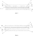
- the embodiment of Fig.4 differs from the embodiment of Fig.3 merely in that the deformation layer 32 being arranged on the first surface of the color filter substrate has a different meaning.
- the first surface of the first substrate refers to a first surface of the color filter substrate.
- the deformation layer 32 may also be made of a thermally-controlled shape memory material.
- the display device further includes a conductive layer 31.
- the conductive layer 31 and the deformation layer 32 are sequentially stacked on any surface of the display panel I from bottom to up.
- the deformation layer 32 reaches the first deformation temperature through heat generated when the conductive layer 31 is energized. This structure is simple and may be easily implemented.
- the conductive layer 31 and the deformation layer 32 may be sequentially stacked on any surface of the display panel I from top to down.
- the so-called “any surface of the display panel I” refers to the first surface 11 of the first substrate, i.e., the first surface of the array susbtrate.
- the terms “top” and “bottom” are defined in accordance with distances of the layers to the first surface 11 of the first substrate.
- a layer close to the first surface 11 of the first substrate is defined as being located at the bottom, while a layer away from the first surface 11 of the first substrate is defined as being located at the top.
- the conductive layer 31 and the deformation layer 32 are arranged on the first surface 11 of the first substrate (i.e., the first surface of the array substrate).
- the deformation layer 32 may be made of a market-available thermally-controlled shape memory material, such as a shape memory polymer (SMP).
- SMP shape memory polymer
- the first deformation temperature of the deformation layer 32 is just a memory temperature of the thermally-controlled shape memory material.
- the first deformation temperature is usually within a range from 80°C to 90°C.
- the first deformation temperature is not limited thereto, and any other temperature may also be set as the first deformation temperature, as long as the design requirements are met.
- the conductive layer 31 may be a transparent conductive layer so as to allow light to pass therethrough.
- the light may pass through the deformation layer 32 by means of the structure or material of the deformation layer 32 itself.
- the display panel I may further include a driver circuit connected to the conductive layer 31.
- the display panel I displays an image under the control of the driver circuit
- the driver circuit mainly functions as to convert a format of a data signal and output the data signal under the control of ta display sequence signal.
- the conductive layer 31 is energized when a high level is inputted by the driver circuit to the conductive layer 31.
- the embodiment of Fig.2 differs from the embodiment of Fig.1 merely in that the conductive layer 31 and the deformation layer 32 being arranged on the first surface 11 of the first susbtrate has a different meaning.
- the first surface 11 of the first susbtrate refers to the first surface of the color filter substrate.
- the deformation layer 32 is configured to, when restoring from the first deformation temperature to a second deformation temperature, enable the display panel I to generate second deformation, so as to enable the display device to achieve flat-surface display.
- the second deformation temperature usually refers to a normal temperature of 20°C to 25°C.
- the second deformation refers to the situation where the display device is changed from the curved-surface display to the flat-surface display.
- the display panel I is configured to achieve the flat-surface display, i.e., the display device is configured to achieve the flat-surface display.
- the deformation layer 32 When the conductive layer 31 is energized, the deformation layer 32 reaches the first deformation temperature (80°C to 90°C) and generates the first deformation, so as to convert the flat-surface display to the curved-surface display, i.e., the display device has a conversion function from the flat-surface display to the curved-surface display.
- the first deformation temperature 80°C to 90°C
- the deformation layer 32 When the conductive layer 31 is deenergized, the deformation layer 32 is restored from the first deformation temperature (80°C to 90°C) to the second deformation temperature (20°C to 25°C) and generates the second deformation, so as to convert the curved-surface display to the flat-surface display, i.e., the display device has a conversion function from the curved-surface display to the flat-surface display.
- the display panel I and the display device are configured to achieve the flat-surface display, i.e., the display device has a pure flat-surface display fucntion.
- the display panel I and the backlight assembly in the related art are each of a curved shape, and this curved shape is maintaned all the time, so an existing curved-surface TV is merely used to achieve the curved-surface display.
- the curvatures of the existing curved-surface TV are set in two ways. In a first mode, a fixed curvature is provided, i.e., the curvature of the curved-surface TV is unique, and accordingly, an optimal viewing point, i.e., a center of the curvature, for the curved-surface TV is unique too.
- an adjustable curvature i.e., the curvature of the curved-surface TV may be adjusted.
- the optical viewing point i.e., a center of the curvature.
- the deformation layer 32 is arranged on any surface of the display panel I in the embodiment of the present disclosure, and the first deformation is generated when the deformation layer 32 reaches the first deformation temperature, so the display device is converted from the flat-surface display to the curved-surface display.
- the deformation layer 32 reaches the second deformation temperature, the second deformation is generated, so the display device is converted from the curved-surface display to the flat-surface display.
- the flat-surface display is provided.
- the display device in the embodiment of the present disclosure has a conversion function from the curved-surface display to the flat-surface display, a conversion function from the flat-surface display to the curved-surface display, and a pure flat-surface display function.
- the display device may be converted from the flat-surface display to the curved-surface display, and when there are several viewers, the pure flat-surface display function may be used, or the display device may be converted from the curved-surface display to the flat-surface display. In this way, it is able to improve the flexibility as well as the user experience.
- the deformation layer 32 on the display panel I it is able to convert from the flat-surface display to the curved-surface display or from the curved-surface display to the flat-surface display.
- the deformation layer 32 on the display panel I it is able to convert from the flat-surface display to the curved-surface display or from the curved-surface display to the flat-surface display.
- the display device is unused, the display device is maintained to have a flat shape, and thereby it is able to provide a well appearance.
- the deformation layer 32 on the display panel I it is able to convert from the flat-surface display to the curved-surface display or from the curved-surface display to the flat-surface display.
- the display device is unused, the display device is maintained to have a flat shape, and then the display device can be transported in flat shape, which helps to reduce bumps when encountering turbulence during transporation, thereby improving safety of products.
- Fig.2 shows the principle for the conversion function from the flat-surface display to curved-surface display, the conversion function from the curved-surface display to the flat-surface display or the pure flat-surface display function of the display device.
- the details may refer to those mentioned in the embodiment as shown in Fig.1 , and will not be repeated herein.
- Fig.3 or Fig.4 shows the principle for the conversion function from the flat-surface display to curved-surface display, the conversion function from the curved-surface display to the flat-surface display or the pure flat-panel display function of the display device.
- the details may refer to those mentioned in the embodiment as shown in Fig.1 , and will not be repeated herein.
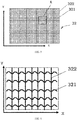
- the deformation layer 32 is formed as a grid including a plurality of segments 322 in a Y-axis direction and a plurality of segments 321 in an X-axis direction.
- the plurality of segments 322 in the Y-axis direction is arranged longitudinally and parallel to each other, and each segment 322 in the Y-axis direction is a straight line.
- the plurality of segments 321 in the X-axis direction is arranged laterally and parallel to each other, and each segment 321 in the X-axis direction is of a predetermined shape (see 321 in Fig.6 ). This structure is simple and may easily be implemented.
- X-axis direction and Y-axis direction are relative concepts to each other, and they are defined in a plane facing a reader.
- a lateral direction is defined as the X-axis direction
- a longitudinal direction is defined as the Y-axis direction.
- Fig.6 is a schematic view showing the deformation layer 32 before being deformed.
- each segment 321 in the X-axis direction is of the predetermined shape, e.g., a waveform shape, and each segment 322 in the Y-axis direction is a straight line.
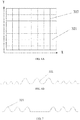
- Fig.6A is a schematic view showing the deformation layer 32 after being deformed.
- the segments 322 in the Y-axis direction are not deformed (i.e., each segment 322 in the Y-axis direction is still maintained as a straight line after the deformation layer 32 is deformed), and each segment 321 in the X-axis direction is deformed and extended as a straight line.
- the display panel I is of a constant size, so the display panel I is curved to achieve the curved-surface display.
- the deformtion layer 32 in Fig.5 may be applied to the display device in Fig.1 .
- the deformation layer 32 is arranged on the first substrate 1, i.e., the array substrate.
- each segment 321 in the X-axis direction is of a waveform shape as shown in Fig.6
- each segment 321 in the X-axis direction is a straight line as shown in Fig.6A .
- the deformation layer 32 is extended to generate the first deformation.
- the deformation layer 32 in Fig.5 may also be applied to the display device in Fig.2 , 3 or 4 .
- the deformation layer 32 is retracted to generate the first deformation.
- the deformation layer 32 is extended to generate the first deformation.
- the deformation layer 32 is retracted so as to generate the first deformation.
- the deformation layer 32 is a grid, and the light may be transmitted through each gap of the grid.
- the deformation layer 32 may be made of a transparent material or a nontransparent material.
- the predetermined shape of each segment 321 in the X-axis direction is a waveform shape. In this way, the structure is simple and may be easily implemented.
- each segment 321 in the X-axis direction is in the predetermined shape, i.e., the waveform shape. In this way, the structure is simple and may be easily implemented.
- each segment 321 in the X-axis direction are in the predetermined shape but arranged non-uniformly.
- the so-called “non-uniformly” refers to the situation where the predetermined shapes are of different sizes and arranged at different densities.
- the predetermined shapes at two end portions of each segment in the X-axis direction have a larger deformation amount (a large bending degree), i.e., small and dense waveform lines are provided at the two end portions.
- the predetermined shapes at a middle portion of each segment in the X-axis direction have a smaller deformation amount (a small bending degree), i.e., large and sparse waveform lines are provided in the middle portion.
- each segment 321 in the X-axis direction is topically provided with the portions with the predetermined shape along the X-axis direction. In this way, it is able to provide the deformation rapidly.
- each segment 321 in the X-axis direction includes a middle portion in shape of a straight line and two end portions each of the predetermined shape. Since the middle portion of the display panel I is unnecessary to be deformed, thus, through the above structure, it is able to provide the deformation rapidly, thereby to achieve the curved-surface display rapidly.
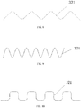
- each segment 321 in the X-axis direction is a mountain-like line. More specifically, all portions of each segment 321 in the X-axis direction are in shape of mountain-like line. In this way, the structure is simple and may easily be implemented.
- the predetermined shape of each segment 321 in the X-axis direction is a hyperbolic curve. More specifically, all portions of each segment 321 in the X-axis direction are in shape of hyperbolic curve. In this way, the structure is simple and may easily be implemented.
- each segment 321 in the X-axis direction is a rectangular wave. More specifically, all portions of each segment 321 in the X-axis direction are in shape of rectangular wave. In this way, the structure is simple and may easily be implemented.
- each segment 321 in the X-axis direction is not limited to the waveform line, the mountain-like line ( Fig.8 ), the hyperbolic curve ( Fig.9 ) or the rectangular wave ( Fig. 10 ), and any other shape may also be applied, as long as the predetermined function may be achieved.
- the deformation amount of the portions of each segment 321 in the X-axis direction may be set in accordance with the size and the curvature of the display panel I, as long as the predetermined function may be achieved.
- the deformation layer 32 includes a plurality of elongated holes 323 arranged regularly. Each elongated hole 323 extends along the Y-axis direction.
- the deformation layer 32 is made of a transparent material.
- X-axis direction and "Y-axis direction” are relative concepts to each other, and they are defined in a plane facing a reader.
- a horizontal direction is defined as the "X-axis direction”
- a longitudinal direction is defined as the "Y-axis direction”.
- each elongated hole 323 in the deformation layer 32 is deformed and extended in the X-axis direction to form an enlarged hole (indicated by 323 shown in Fig. 12 ).
- the display panel I is deformed at a certain curvature due to the internal force generated when the deformation layer 32 is deformed, so as to enable the display device to be curved relative to the Y-axis direciotn, thereby to enable the display device to be converted from the flat-surface display to the curved-surface display.
- each enlarged elongated hole 323 is restored from the shape shown in Fig.
- each enlarged elongated hole 323 is restored to the elongated hole 323 (shown in Fig. 11 ), and then the purpose of conversion from the curved-surface display to the flat-surface is achieved.
- the deformation layer in Fig.1, 2 , 3 or 4 may be used in Fig.11 .
- each elongated hole 323 may be a fusiform hole. In this way, the structure is simple and may easily be implemented.
- each elongated hole 323 may be a rectangular hole. In this way, the structure is simple and may easily be implemented.
- each elongated hole 323 may not be limtied to the fusiform hole or rectangular hole, and it may be of any other shape, as long as the deformation may be achieved.
- the elongated holes 323 are arranged symmatrically relative to a longitudinal center line of the deformation layer 32. In this way, the structure is simple and may be easily implemented.
- the elongated holes 323 are arranged evenly, so as to achieve the deformation evenly.
- the elongated holes 323 are arranged unevenly, so as to achieve the deformation rapidly.
- the elongated holes 323 are arranged sparser in the middle of the deformation layer and denser at the two ends of the deformation layer. Since the display panel I is unnecessary to be deformed in the middle, thus, through this structure, it is able to achieve the curved-surface display rapidly.
- the deformation layer 32 is extended to generate the first deformation.
- the deformation layer 32 is provided with the predetermined shape (indicated by 321 in Fig.6 ) at the second deformation temperature (20°C to 25°C), and generates the first deformation at the first deformation temperature (80°C to 90°C) and generates the second deformation at the second deformation temperature (20°C to 25°C).
- the deformation layer 32 in Figs.2-13 may be also be extended to generate the first deformation.
- the first deformation temperature may be 20°C to 25°C, or any other temperatures
- the second deformation temperature may be 80°C to 90°C, or any other temperatures.
- the deformation temperatures may be set in accordance with process conditions, such as properties of liquid crystals, the deformation layer or any other material, and temperature range for the manufacture.
- the deformation layer 32 may also be retracted to generate the first deformation. Different from the situation where the deformation layer 32 is extended to generate the first deformation, in this embodiment, the deformation layer 32 is provided with the predetermined shape (indicated by 321 in Fig.6 ) at the first deformation temperature (80°C to 90°C). The deformation layer 32 generates the first deformation (the conversion from the flat-surface display to the curved-surface display) at the first deformation temperature, and generates the second deformation (the conversion from the curved-surface display to the flat-surface display) at the second deformation temperature (20°C to 25°C).
- the deformation layer 32 in Figs.2-13 may be retracted to generate the first deformation.
- the first deformation temperature may be 20°C to 25°C, or any other temperature
- the second deformation temperature may be 80°C to 90°C, or any other temperature.
- the deformation temperatures may be set in accordance with process conditions, such as properties of liquid crystals, the deformation layer or any other material, and temperature range for the manufacture.
- the display device 100 may further include a processing module 6 configured to calculate the deformation amount of the deformation layer 32 in accordance with the curvature, and calculate the first deformation temperature in accordance with the deformation amount.
- the display device 100 adjusts temperatures in accordance with the first deformation temperature, so as to generate the first deformation.
- a plurality of predetermined curvatures may be provided, and one of them may be selected by the viewer.
- the first deformation temperature correspoding to the selected curvature is calculated by the processing module 6, so as to enable the deformation layer 32 to generate the first deformation, thereby to enable the display device 100 to achieve the curved-surface display at the selected curvature.
- the processing module 6 may be applied to the display device in Figs. 1-4 .
- the display device 100 may further include a sensing module 7 and a distance measuring unit 8.
- the sensing module 7 is connected to the processing module 6 via the distance measuring unit 8.
- the sensing module 7 is configured to detect a position of the viewer.
- the distance measuring unit 8 is configured to acquire a distance L between the viewer and the display panel and convert it into the curvature. For example, the distance measuring unit 8 may convert the distance L into an optimal curvature suitable for the viewer at the position.
- the processing module 6 is configured to calculate the deformation amount of the deformation layer 32 in accordance with the curvature, and calculate the first deformation temperature in accordance with the deformation amount.
- the position of the viewer is detected by the sensing module 7, the distance between the viewer and the display panel is calculated by the distance measuring unit 8, and the curvature is acquired in accordance with the distance.
- the deformation amount of the deformation layer 32 corresponding to the curvature is calculated by the processing module 6, and the first deformation temperature is calculated in accordance with the deformation amount.
- the deformation layer 32 generates the first deformation in accordance with the first deformation temperature, so as to enable the display device 100 to achieve the curved-surface display at the curvature.
- the above operation may be repeated so as to achieve the curved-surface display at different curvatures, theretby to provide the viewers at different positions with an optimal viewing effect.
- the processing module 6 may be applied to the display device in Figs. 1-4 .
- the first substrate 1 and the second substrate 2 may be a resin substrate or a glass substrate.
- the first substrate 1 and the second substrate 2 are not limited thereto, and any other substrate may also be used, as long as the design requirement may be met.
- the display panel I may further include a first polarizer 4 arranged above the first substrate 1 and a second polarizer 5 arranged below the second substrate 2.
- the terms “above” and “below” are relative concepts to each other, and they just refer to the positions as viewed in Fig.1 .
- the display device is not limited to the TV, and it may also be any product or member having a display function, such as a liquid crystal display panel, an Oragnic Light-Emitting Diode (OLED) panel, a mobile phone, a flat-panel computer, a display, a laptop computer, a digital photo frame or a navigator.
- a display function such as a liquid crystal display panel, an Oragnic Light-Emitting Diode (OLED) panel, a mobile phone, a flat-panel computer, a display, a laptop computer, a digital photo frame or a navigator.
- the display device when it is a mobile phone, a flat-panel computer, a display or a laptop computer, it may further include a backlight assembly.
- the backlight assembly also has a conversion function from the curved-surface display to the flat-surface display and a conversion function from the flat-surface display to the curved-surface display.
- the backlight assembly may be made of a shape memory polymer or a shape memory polymer alloy with a certain mechanical strength, and assembled with the display panel I by injection-molding or any other methods, so as to be deformed together with the display panel I.
- the present disclosure provides in this embodiment a method for manfuacturing the display device, which includes following steps.
- Step S200 of forming the display panel I (referring to Fig. 1, 2 , 3 or 4 ) and Step S300 of assembling the display panel I (referring to Fig. 1, 2 , 3 or 4 ) with the other components of the display device are identical to those known in the art.
- the display device manufactured in this embodiment is compeltely the same as that mentioned in the first embodiment, so the structures thereof are not repeated herein.
- the method since the method includes all contents of the display device in the first embodiment, thus, the method can obtain all effects of the display device.
- the deformation layer 32 is arranged on any surface of the display panel I. When reaching the first deformation temperature, the deformation layer 32 generates the first deformation, and applies an internal force onto the display panel I. Because the display panel I is of a constant size, as shown in Fig.1A , the display panel I may be curved due to the internal force, so as to achieve the curved-surface display. In other words, the display panel I in the embodiment of the present disclosure is curved due to the internal force generated by itself, and the curved shape may be always maintained under the effect of the internal force. As a result, it is unnecessary to maintain the curved shape of the display panel using a shell of an existing backlight assembly, and thereby it is able to reduce the assembly difficulty.
- the deformation layer 32 is arranged on any surface of the display panel I so as to achieve the curved-surface display, and it is unnecessary to maintain the curved shape of the display panel using the shell of the existing backlight assembly, so the integration of the display panel I can be improved.
- the deformation layer 32 is arranged on any surface of the display panel I so as to achieve the curved-surface display, and it is unnecessary to maintain the curved shape of the display panel using the shell of the existing backlight assembly, so the display panel may be aplied to a transparent display device without any backlight assembly, thereby to provide a wider application range.
- the deformation layer 32 is arranged on any surface of the display panel I so as to achieve the curved-surface display, and it is unnecessary to maintain the curved shape of the display panel using the shell of the existing backlight assembly, so a light and thin display device is provided.
- the first substrate 1 is an array substrate
- the second substrate 2 is a color filter substrate.
- the first surface 11 of the first substrate refers to a surface of the first substrate away from the second substrate 2, and the other surface is just the second surface 12 of the first substrate.
- the first surface 21 of the second substrate refers to a surface of the second substrate away from the first substrate 1, and the other surface is just the second surface 22 of the second substrate.
- first substrate 1 and the second substrate 2 are relative concepts to each other, and referring to Fig.2 or 4 , the first substrate 1 may also be a color filter substrate, while the second substrate 2 may also be an array substrate.
- the first substrate 1 is an array substrate (as shown in Fig.1 or 3 ), and before the formation of the deformation layer 32 (as shown in Fig.1 or 3 ) onto the first surface 11 of the first substrate (as shown in Fig.1 or 3 ), the patterns for the array susbtrate (indicated by 1 in Fig.1 or 3 ) have been formed on the second surface 12 of the first substrate (as shown in Fig.1 or 3 ).
- Fig.17 is a flow chart of a method for forming the deformation layer
- Fig.18 is a schematic view showing the formation of the deformation layer.
- the manufacture of the structure in Fig.1 or 2 is taken as an example.
- the deformation 32 may be made of a thermally-controlled shape memory material 32A, and the display device may further include the conductive layer 31.
- Step S100 of forming the deformation layer 32 (referring to Fig. 18 ) on the first surface 11 (referring to Fig. 18 ) of the first substrate includes following steps.
- This process is simple and may be easily performed.
- the method in Fig.17 may also be used to manufacture the deformation layer 32 in Fig.11 or 13 .
- the conductive layer 31 is formed on the first surface 11 of the first substrate by sputtering.
- the reserved photoresist partially overlaps a black matrix Y of the display panel I (referring to Fig. 1 or 2 ), so as to prevent the light transmittance from being adversely affected as possible.
- the deformation layer 32 may be made of a transparent material, i.e., the thermally-controlled shape memory material 32A is transparent.
- Step S103 (referring to Fig. 17 ) of removing the remaining photoresist from the first substrate 1 (referring to Fig. 1 or 2 ) with the thermally-controlled shape memory material 32A includes: removing the remaining photoresist from the first substrate 1 (referring to Fig. 1 or 2 ) with the thermally-controlled shape memory material 32A using a secondary exposing and developing process 32B.
- This process is simple and may be performed conveniently.
- the deformation layer 32 may also be made of a nontransparent material, i.e., the thermally-controlled shape memory material 32A is nontransparent.
- Step S103 (refering to Fig. 17 ) of removing the remaining photoresist from the first substrate 1 (referring to Fig. 1 or 2 ) with the thermally-controlled shape memory material 32A includes: removing the remaining photoresist from the first substrate 1 (referring to Fig. 1 or 2 ) with the thermally-controlled shape memory material 32A using an alkaline stripping liquid.
- This process is simple and may be performed conveniently.
- Fig.19 is another flow chart of a method for forming the deformation layer
- Fig.20 is a schematic view showing the formation of the deformation layer.
- the manfuacture of the structure in Fig.3 or 4 will be taken as an example.
- the deformation layer 32 (referring to Fig. 20 ) may be made of an electrically-controlled shape memory material 32C, and Step S100 (referring to Fig. 20 ) of forming the deformation layer 32 (referring to Fig. 20 ) on the first surface 11 (referring to Fig. 20 ) of the first substrate includes following steps.
- This process is simple and may be performed conveniently.
- the reserved photoresist may partially overlap the black matrix Y of the display panel I, so as to prevent the light transmittance from being adversely affected as possible.
- the deformation layer 32 may be made of a transparent material, i.e., the electrically-controlled shape memory material 32C is transparent.
- Step S105 (referring to Fig. 19 ) of removing the remaining photoresist from the first substrate 1 (referring to Fig. 3 or 4 ) with the electrically-controlled shape memory material 32C includes: removing the remaining photoresist from the first substrate 1 (referring to Fig. 3 or 4 ) with the electrically-controlled shape memory matrial 32C using a seecondary exposing and developing process 32B.
- This process is simple and may be performed conveniently.
- the deformation layer 32 may also be made of a nontransparent material, i.e., the electrically-controlled shape memory material 32C is nontransparent.
- Step S105 (referring to Fig. 19 ) of removing the remaining photoresist from the substrate 1 (referring to Fig. 3 or 4 ) with the electrically-controlled shape memory material 32C includes: removing the remaining photoresist from the first substrate 1 (referring to Fig. 3 or 4 ) with the electrically-controlled shape memory material 32C using an alkaline stripping liquid.
- This process is simple and may be performed conveniently.
Landscapes
- Engineering & Computer Science (AREA)
- Physics & Mathematics (AREA)
- Theoretical Computer Science (AREA)
- General Physics & Mathematics (AREA)
- General Engineering & Computer Science (AREA)
- Computer Hardware Design (AREA)
- Nonlinear Science (AREA)
- Human Computer Interaction (AREA)
- Chemical & Material Sciences (AREA)
- Crystallography & Structural Chemistry (AREA)
- Mathematical Physics (AREA)
- Optics & Photonics (AREA)
- Devices For Indicating Variable Information By Combining Individual Elements (AREA)
- Multimedia (AREA)
- Signal Processing (AREA)
Description
- The present application claims a priority of the Chinese patent application No.
201510093404.4 filed on March 2, 2015 - The present disclosure relates to the field of display technology, in particular to a display device and a method for manufacturing the same.
- Depending on their shapes, display devices may be divided into flat-panel display devices and curved-surface display devices. The flat-panel display devices include televisions (TVs), liquid crystal display panels, electronic papers, organic light-emitting diode (OLED) panels, mobile telephones or flat-panel computers, etc. The curved-surface display devices include curved-surface televisions, curved-surface mobile phones or curved-surface computers.
- Taking the curved-surface television as an example, it refers to a television which has a curved-surface display function and which is provided with a curved-surface characteristic in conformity with that of an eyeball so as to provide an equal distance between each point on a screen and an eye. The curved-surface television includes a display panel and a backlight assembly. A first substrate and a second substrate are arranged opposite to each other to form a cell, thereby to form the display panel. Usually, an external mechanical force is applied to the display panel so as to curve it, and a curved shape of the display panel is maintained by a shell in the backlight assembly.
- However, it is found by the inventor that, it is difficult to assemble the curved-surface television when the curved shape of the display panel is maintained by the shell in the backlight assembly.
- The present disclosure provides a display device and a method for manufacturing the same, which can solve the problem in the relayed art that it is difficult to assemble the curved-surface television.
- In one aspect, the present disclosure provides in some embodiments a display device, including a first substrate and a second substrate which are arranged opposite to each other to form a display panel. A deformation layer is arranged at any surface of the display panel and configured to enable the display panel to generate first deformation when it reaches a first deformation temperature, so as to enable the display device to achieve curved-surface display.
- Alternatively, the deformation layer is extended or retracted so as to generate the first deformation.
- Alternatively, the deformation layer is made of an electrically-controlled shape memory material and reaches the first deformation temperature through heat generated when it is energized.
- Alternatively, the electrically-controlled shape memory material is a shape memory polymer doped with conductive carbon black, metallic powder or conductive polymer.
- Alternatively, the display panel further includes a driver circuit connected to the deformation layer.
- Alternatively, the deformation layer is made of a thermally-controlled shape memory material, the display device further includes a conductive layer, the conductive layer and the deformation layer are arranged on any surface of the display panel from the bottom up, and the deformation layer reaches the first deformation temperature through heat generated when the conductive layer is energized.
- Alternatively, the thermally-controlled shape memory material is a shape memory polymer.
- Alternatively, the display panel further includes a driver circuit connected to the conductive layer.
- Alternatively, the deformation layer is configured to enable the display panel to generate a second deformation when it is restored from the first deformation temperature to a second deformation temperature, so as to enable the display device to achieve flat-panel display.
- Alternatively, the first deformation temperature is 80°C to 90°C and the second deformation temperature is 20°C to 25°C, or the first deformation temperature is 20°C to 25°C and the second deformation temperature is 80°C to 90°C.
- Alternatively, the deformation layer is formed as a grid including a plurality of segments in a Y-axis direction and a plurality of segments in an X-axis direction, the plurality of segments in the Y-axis direction is arranged longitudinally and parallel to each other, each segment in the Y-axis direction is a straight line, the plurality of segments in the X-axis direction is arranged laterally and parallel to each other, and each segment in the X-axis direction is provided with a predetermined shape.
- Alternatively, the predetermined shape of each segment in the X-axis direction is a waveform line, a mountain-like line, a hyperbolic curve or a rectangular-wave.
- Alternatively, all portions of each segment in the X-axis direction are in a shape of the predetermined shape.
- Alternatively, the portions of each segment in the X-axis direction are arranged non-uniformly; the predetermined shape at two end portions of each segment in the X-axis direction has a larger deformation amount; the predetermined shape at a middle portion of each segment in the X-axis direction has a smaller deformation amount.
- Alternatively, each segment in the X-axis direction is topically in a shape of the predetermined shape.
- Alternatively, each segment in the X-axis direction includes a middle portion in a shape of a straight-line, and two end portions each in a shape of the predetermined shape.
- Alternatively, the deformation layer includes a plurality of elongated holes arranged regularly, and each elongated hole extends along the Y-axis direction.
- Alternatively, each elongated hole is of a fusiform hole or rectangular hole.
- Alternatively, the elongated holes are arranged symmetrically relative to a Y-axis direction of the deformation layer.
- Alternatively, the elongated holes are arranged evenly.
- Alternatively, when the deformation layer reaches the first deformation temperature, each elongated hole is deformed and extends in the X-axis direction to form an enlarged hole.
- Alternatively, the elongated holes are arranged unevenly.
- Alternatively, the elongated holes are arranged sparser in the middle of the deformation layer and denser at the two ends of the deformation layer.
- Alternatively, the display device further includes a processing module configured to calculate the deformation amount of the deformation layer in accordance with a curvature, and calculate the first deformation temperature in accordance with the deformation amount.
- Alternatively, the display device further includes a sensing module and a distance measuring unit through which the sensing module is connected to the processing module. The sensing module is configured to detect a viewer's position, and the distance measuring unit is configured to acquire a distance between the viewer and the display device and convert the distance into the curvature.
- In another aspect, the present disclosure provides in some embodiments a method for manufacturing a display device, including steps of: forming a deformation layer on a first surface of a first substrate; arranging a second surface of the first substrate and a second substrate opposite to each other, thereby forming a display panel; assembling the display panel with further components, thereby forming a complete display device; and enabling, by the deformation layer at a first deformation temperature, the display panel to be curved and generate first deformation to enable the display device to achieve curved-surface display, and maintaining the first deformation for a predetermined period of time.
- Alternatively, the first substrate is an array substrate, and before the formation of the deformation layer on the first surface of the first substrate, patterns have been formed on the second surface of the first substrate.
- Alternatively, the deformation layer is made of a thermally-controlled shape memory material, and the display device further includes a conductive layer. The step of forming the deformation layer on the first surface of the first substrate includes: forming the conductive layer on the first surface of the first substrate, and reserving room for wires of a circuit; applying a photoresist layer onto a surface of the conductive layer, and exposing and developing the photoresist layer; and applying the thermally-controlled shape memory material onto a surface of the exposed and developed photoresist layer, and removing the remaining photoresist from the first substrate with the thermally-controlled shape memory material.
- Alternatively, the deformation layer is made of an electrically-controlled shape memory material, and the step of forming the deformation layer on the first surface of the first substrate includes: applying a photoresist layer onto the first surface of the first substrate, and exposing and developing the photoresist; and applying the electrically-controlled shape memory material onto a surface of the exposed and developed photoresist layer, reserving sufficient room for wires of a circuit, and removing the remaining photoresist from the first substrate with the electrically-controlled shape memory material.
- Alternatively, the deformation layer is made of a transparent material, and the step of removing the remaining photoresist from the first substrate with the thermally-controlled or electrically-controlled shape memory material includes removing the remaining photoresist from the first substrate with the thermally-controlled or electrically-controlled shape memory material by a secondary exposing and developing process.
- Alternatively, the deformation layer is made of a nontransparent material, and the step of removing the remaining photoresist from the first substrate with the thermally-controlled or electrically-controlled shape memory material includes removing the remaining photoresist from the first substrate with the thermally-controlled or electrically-controlled shape memory material using an alkaline stripping liquid.
- According to the embodiments of the present disclosure, the deformation layer is arranged on any surface of the display panel, and when the deformation layer reaches the first deformation temperature, the deformation is generated so as to apply an internal force to the display panel. Because the display panel is of a constant size, it will be curved due to the internal force, so as to achieve the curved-surface display. In other words, the display panel in the embodiments of the present disclosure is curved under the effect of the internal force generated by itself, and it may be always maintained at the curved shape when the internal force is applied continuously. As a result, it is unnecessary to maintain the curved shape of the display panel with a shell of an existing backlight assembly, and thereby it is able to reduce the assembly difficulty.
- In order to illustrate the technical solutions of the present disclosure in a clearer manner, the drawings desired for the present disclosure will be described hereinafter briefly. Obviously, the following drawings merely relate to some embodiments of the present disclosure, and based on these drawings, a person skilled in the art may obtain the other drawings without any creative effort.
-
Fig.1 is a schematic view showing a display device before being deformed according to one embodiment of the present disclosure; -
Fig.1A is a schematic view showing the display device inFig.1 after being deformed; -
Fig.2 is another schematic view showing the display device before being deformed according to one embodiment of the present disclosure; -
Fig.3 is yet another schematic view showing the display device before being deformed according to one embodiment of the present disclosure; -
Fig.4 is still yet another schematic view showing the display device before being deformed according to one embodiment of the present disclosure; -
Fig.5 is a schematic view showing a deformation layer before being deformed according to one embodiment of the present disclosure; -
Fig.6 is a topically enlarged view of portion A inFig.5 ; -
Fig.6A is a schematic view showing segments in an X-axis direction and segments in a Y-axis direction inFig.6 after being deformed; -
Fig.6B is a schematic view showing the segment in the X-axis direction provided with an irregular predetermined shape inFig.6 ; -
Fig.7 is another schematic view showing the segment in the X-axis direction before being deformed according to one embodiment of the present disclosure; -
Fig.8 is yet another schematic view showing the segment in the X-axis direction before being deformed according to one embodiment of the present disclosure; -
Fig.9 is still yet another schematic view showing the segment in the X-axis direction before being deformed according to one embodiment of the present disclosure; -
Fig.10 is still yet another schematic view showing the segment in the X-axis direction before being deformed according to one embodiment of the present disclosure; -
Fig.11 is another schematic view showing the deformation layer before being deformed according to one embodiment of the present disclosure; -
Fig. 12 is a schematic view showing the deformation layer inFig.11 after being deformed; -
Fig. 13 is yet another schematic view showing the deformation layer before being deformed according to one embodiment of the present disclosure; -
Fig. 14 is a logic control diagram of the display device for achieving the curved-surface display according to one embodiment of the present disclosure; -
Fig. 15 is another logic control diagram of the display device for achieving the curved-surface display according to one embodiment of the present disclosure; -
Fig. 16 is a flow chart of a method for manufacturing a display device according to one embodiment of the present disclosure; -
Fig.17 is a flow chart of a method for forming the deformation layer according to one embodiment of the present disclosure; -
Fig.18 is a schematic view showing the formation of the deformation layer according to one embodiment of the present disclosure; -
Fig.19 is another flow chart of the method for forming the deformation layer according to one embodiment of the present disclosure; and -
Fig.20 is a schematic view showing the formation of the deformation layer according to one embodiment of the present disclosure. -
- I
- display panel
- 1
- first substrate
- 11
- first surface of first substrate
- 12
- second surface of first substrate
- 2
- second substrate
- 21
- first surface of second substrate
- 22
- second surface of second substrate
- 31
- conductive layer
- 32
- deformation layer
- 32A
- thermally-controlled shape memory material
- 32B
- secondary exposing and developing process
- 32C
- electrically-controlled shape memory material
- 321
- segment in X-axis direction
- 322
- segment in Y-axis direction
- 323
- elongated hole
- 33
- photoresist layer
- 34
- exposed and developed surface of photoresist layer
- 4
- first polarizer
- 5
- second polarizer
- 6
- processing module
- 7
- sensing module
- 8
- distance measuring unit
- 100
- display device
- In order to make the objects, the technical solutions and the advantages of the present disclosure more apparent, embodiments of the present disclosure will be described hereinafter in conjunction with the drawings.
- As shown in
Fig.1 , the present disclosure provides in this embodiment a display device, which includes afirst substrate 1 and asecond substrate 2 arranged opposite to each other to form a display panel I. - A
deformation layer 32 is arranged at any surface of the display panel I . Thedeformation layer 32 is configured to, when reaching a first deformation temperature, enable the display panel I to generate first deformation, so as to enable the display device to achieve curved-surface display. - As shown in
Fig. 1 , the any surface of the display panel I refers to a surface of the display panel I exposed to the outside, i.e., afirst surface 11 of the first substrate or afirst surface 21 of the second substrate. Thefirst surface 11 of the first substrate refers to a surface of the first substrate away from thesecond substrate 2, and thefirst surface 21 of the second substrate refers to a surface of the second substrate away from thefirst substrate 1. - As is known in the art, the display panel I includes a color filter substrate and an array substrate. A substrate of the display panel I facing a viewer is the color filter substrate, while the other substrate is the array susbtrate.
- In this embodiment, the display panel I includes the
first substrate 1 and thesecond substrate 2. It should be appreciated that, thefirst substrate 1 and thesecond substrate 2 are relative concepts to each other. To be specific, thefirst substrate 1 may be the color filter substrate or the array substrate, while thesecond substrate 2 may be the array substrate or the color filter substrate. When one substrate is defined as thefirst substrate 1, the other substrate of the display panel I is just thesecond substrate 2. - In
Figs.1, 2 ,3 and 4 , the substrate where thedeformation layer 32 is arranged is defined as thefirst substrate 1. - More specifically, as shown in
Fig.1 , an upper surface of the display panel I, i.e., a surface facing the viewer, is defined as a display surface. Thesecond substrate 2 faces the viewer, so thesecond substrate 2 is the color filter substrate and thefirst substrate 1 is the array substrate. The terms "upper" and "lower" are relative concepts to each other, and takingFig.1 as an example, "upper" and "lower" just refer to the positions as viewed inFig.1 . - Similarly, as shown in
Fig.2 , thefirst substrate 1 is the color filter substrate while thesecond substrate 2 is the array substrate. - Similarly, as shown in
Fig.3 , thesecond substrate 2 is the color filter substrate while thefirst substrate 1 is the array substrate. - Similarly, as shown in
Fig.4 , thefirst substrate 1 is the color filter substrate while thesecond substrate 2 is the array substrate. - In this embdiment, the first deformation refers to the situation where the display device is changed from flat-surface display to curved-surface display.
- As shown in
Fig. 1A , the so-called "curved-surface display" refers to the situation where the display panel I is curved in such a manner as to be in conformity with a curve characteristic of an eyeball. When the eyeball of the viewer is located at an optimal viewing point (i.e., at a center of a curvature), there is an equal distance between each point on the display panel I and the eyeball of the viewer. - As shown in
Fig. 1 , according to the embodiment of the present disclosure, thedeformation layer 32 is arranged on any surface of the display panel I. When reaching the first deformation temperature, thedeformation layer 32 generates the first deformation, and applies an internal force onto the display panel I. Because the display panel I is of a constant size, as shown inFig.1A , the display panel I may be curved due to the internal force, so as to achieve the curved-surface display. In other words, the display panel I in the embodiment of the present disclosure is curved due to the internal force generated by itself, and the curved shape may be always maintained under the effect of the internal force. As a result, it is unnecessary to maintain the curved shape of the display panel using a shell of an existing backlight assembly, and thereby reducing the assembly difficulty. - In addition, in the embodiment of the present disclosure, the
deformation layer 32 is arranged on any surface of the display panel I so as to achieve the curved-surface display, and it is unnecessary to maintain the curved shape of the display panel using the shell of the existing backlight assembly, so the integration of the display panel I is improved. - In addition, in the embodiment of the present disclosure, the
deformation layer 32 is arranged on any surface of the display panel I so as to achieve the curved-surface display, and it is unnecessary to maintain the curved shape of the display panel using the shell of the existing backlight assembly, so the display panel may be applied to a transparent display device without any backlight assembly, thereby to provide a wider application range. - In addition, in the embodiment of the present disclosure, the
deformation layer 32 is arranged on any surface of the display panel I so as to achieve the curved-surface display, and it is unnecessary to maintain the curved shape of the display panel using the shell of the existing backlight assembly, so a light and thin display device can be provided. - As shown in
Fig. 3 , thedeformation layer 32 may be made of an electrically-controlled shape memory material. Thedeformation layer 32 reaches the first deformation temperature through heat generated when thedeformation layer 32 is energized. To be specific, thedeformation layer 32 is arranged on thefirst surface 11 of the first substrate, i.e., the first surface of the array substrate. - As shown in
Fig. 3 , when thedeformation layer 32 reaches the first deformation temperature through the heat generated when it is energized, it is able to prevent an operation temperature of the display device from being adversely affected by the first deformation temperature. - As shown in
Fig. 3 , more specifically, the electrically-controlled shape memory material adopted by thedeformation layer 32 may be a market-available material. The electrically-controlled shape memory material may be a shape memory polymer (SMP) doped with conductive carbon black, metallic powder or conductive polymer. - As shown in
Fig. 3 , thedeformation layer 32 reaching the first deformation temperature refers to reaching a memory temperature of the electrically-controlled shape memory material. - More specifically, considering the operation temperature of the display device, the first deformation temperature is usually within a range from 80°C to 90°C. Of course, it should be appreciated that, the first deformation temperature is not limited thereto, and any other temperature may also be set as the first deformation temperature, as long as the design requirements are met.
- As shown in
Fig. 3 , the display panel I may further include a driver circuit (not shown) connected to thedeformation layer 32. - As is known in the art, the display panel I displays an image under the control of the driver circuit, and the driver circuit mainly functions as to convert a format of a data signal and output the data signal under the control of the display sequence signal. The
deformation layer 32 is energized when a high level is inputted by the driver circuit to thedeformation layer 32. - The embodiment of
Fig.4 differs from the embodiment ofFig.3 merely in that thedeformation layer 32 being arranged on the first surface of the color filter substrate has a different meaning. In this embodiemnt, the first surface of the first substrate refers to a first surface of the color filter substrate. - As shown in
Fig. 1 , thedeformation layer 32 may also be made of a thermally-controlled shape memory material. The display device further includes aconductive layer 31. Theconductive layer 31 and thedeformation layer 32 are sequentially stacked on any surface of the display panel I from bottom to up. Thedeformation layer 32 reaches the first deformation temperature through heat generated when theconductive layer 31 is energized. This structure is simple and may be easily implemented. - Of course, it should be appreciated that, the
conductive layer 31 and thedeformation layer 32 may be sequentially stacked on any surface of the display panel I from top to down. - As shown in
Fig. 1 , the so-called "any surface of the display panel I" refers to thefirst surface 11 of the first substrate, i.e., the first surface of the array susbtrate. In the embodiments of the present disclosure, the terms "top" and "bottom" are defined in accordance with distances of the layers to thefirst surface 11 of the first substrate. To be specific, a layer close to thefirst surface 11 of the first substrate is defined as being located at the bottom, while a layer away from thefirst surface 11 of the first substrate is defined as being located at the top. - As shown in
Fig.1 , theconductive layer 31 and thedeformation layer 32 are arranged on thefirst surface 11 of the first substrate (i.e., the first surface of the array substrate). - As shown in
Fig.1 , thedeformation layer 32 may be made of a market-available thermally-controlled shape memory material, such as a shape memory polymer (SMP). - The first deformation temperature of the
deformation layer 32 is just a memory temperature of the thermally-controlled shape memory material. - Specifically, considering the operation temperature of the display device, the first deformation temperature is usually within a range from 80°C to 90°C. Of course, it should be appreciated that, the first deformation temperature is not limited thereto, and any other temperature may also be set as the first deformation temperature, as long as the design requirements are met.
- As shown in
Fig. 1 , theconductive layer 31 may be a transparent conductive layer so as to allow light to pass therethrough. The light may pass through thedeformation layer 32 by means of the structure or material of thedeformation layer 32 itself. - As shown in
Fig. 1 , in this embodiment, the display panel I may further include a driver circuit connected to theconductive layer 31. - As is known in the art, the display panel I displays an image under the control of the driver circuit, and the driver circuit mainly functions as to convert a format of a data signal and output the data signal under the control of ta display sequence signal. The
conductive layer 31 is energized when a high level is inputted by the driver circuit to theconductive layer 31. - The embodiment of
Fig.2 differs from the embodiment ofFig.1 merely in that theconductive layer 31 and thedeformation layer 32 being arranged on thefirst surface 11 of the first susbtrate has a different meaning. In this embodiment, thefirst surface 11 of the first susbtrate refers to the first surface of the color filter substrate. - As shown in
Fig. 1 (or, Fig. 2 , orFig. 3, or Fig. 4 ), thedeformation layer 32 is configured to, when restoring from the first deformation temperature to a second deformation temperature, enable the display panel I to generate second deformation, so as to enable the display device to achieve flat-surface display. - The second deformation temperature usually refers to a normal temperature of 20°C to 25°C. The second deformation refers to the situation where the display device is changed from the curved-surface display to the flat-surface display.
- As shown in
Fig. 1 , an operation procedure will be described hereinafter by taking the display device inFig.1 as an example. When the display device is started, the display panel I is configured to achieve the flat-surface display, i.e., the display device is configured to achieve the flat-surface display. - When the
conductive layer 31 is energized, thedeformation layer 32 reaches the first deformation temperature (80°C to 90°C) and generates the first deformation, so as to convert the flat-surface display to the curved-surface display, i.e., the display device has a conversion function from the flat-surface display to the curved-surface display. - When the
conductive layer 31 is deenergized, thedeformation layer 32 is restored from the first deformation temperature (80°C to 90°C) to the second deformation temperature (20°C to 25°C) and generates the second deformation, so as to convert the curved-surface display to the flat-surface display, i.e., the display device has a conversion function from the curved-surface display to the flat-surface display. - When the display device is started and the
conductive layer 31 is not energized, thedeformation layer 32 has no change. At this point, the display panel I and the display device are configured to achieve the flat-surface display, i.e., the display device has a pure flat-surface display fucntion. - It is found by the inventor that, the display panel I and the backlight assembly in the related art are each of a curved shape, and this curved shape is maintaned all the time, so an existing curved-surface TV is merely used to achieve the curved-surface display. It is also found that, the curvatures of the existing curved-surface TV are set in two ways. In a first mode, a fixed curvature is provided, i.e., the curvature of the curved-surface TV is unique, and accordingly, an optimal viewing point, i.e., a center of the curvature, for the curved-surface TV is unique too. In a second mode, an adjustable curvature is provided, i.e., the curvature of the curved-surface TV may be adjusted. Once the curvature has been adjusted, the optical viewing point, i.e., a center of the curvature, is also fixed. Regardless of the setting modes of the curvatures, there is only one optical viewing point for the curved-surface TV, so a better effect may be achieved when there is a single viewer. However, when there are several viewers, it is unable to achieve an ideal viewing effect.
- As shown in
Fig. 1 , as compared with the related art, thedeformation layer 32 is arranged on any surface of the display panel I in the embodiment of the present disclosure, and the first deformation is generated when thedeformation layer 32 reaches the first deformation temperature, so the display device is converted from the flat-surface display to the curved-surface display. When thedeformation layer 32 reaches the second deformation temperature, the second deformation is generated, so the display device is converted from the curved-surface display to the flat-surface display. When the display device is started, the flat-surface display is provided. In other words, the display device in the embodiment of the present disclosure has a conversion function from the curved-surface display to the flat-surface display, a conversion function from the flat-surface display to the curved-surface display, and a pure flat-surface display function. When there is only one viewer, the display device may be converted from the flat-surface display to the curved-surface display, and when there are several viewers, the pure flat-surface display function may be used, or the display device may be converted from the curved-surface display to the flat-surface display. In this way, it is able to improve the flexibility as well as the user experience. - In addition, through the
deformation layer 32 on the display panel I, it is able to convert from the flat-surface display to the curved-surface display or from the curved-surface display to the flat-surface display. As a result, it is unnecessary to provide a backplate corresponding to the display device with a curved shape, thereby to faclitate the installation of the display device, e.g., it may be placed on a desk or hung on the wall. - In addition, through the
deformation layer 32 on the display panel I, it is able to convert from the flat-surface display to the curved-surface display or from the curved-surface display to the flat-surface display. As a result, when the display device is unused, the display device is maintained to have a flat shape, and thereby it is able to provide a well appearance. - In addition, through the
deformation layer 32 on the display panel I, it is able to convert from the flat-surface display to the curved-surface display or from the curved-surface display to the flat-surface display. As a result, when the display device is unused, the display device is maintained to have a flat shape, and then the display device can be transported in flat shape, which helps to reduce bumps when encountering turbulence during transporation, thereby improving safety of products. -
Fig.2 shows the principle for the conversion function from the flat-surface display to curved-surface display, the conversion function from the curved-surface display to the flat-surface display or the pure flat-surface display function of the display device. The details may refer to those mentioned in the embodiment as shown inFig.1 , and will not be repeated herein. -
Fig.3 or Fig.4 shows the principle for the conversion function from the flat-surface display to curved-surface display, the conversion function from the curved-surface display to the flat-surface display or the pure flat-panel display function of the display device. The details may refer to those mentioned in the embodiment as shown inFig.1 , and will not be repeated herein. - Referring to
Figs.5-6 , thedeformation layer 32 is formed as a grid including a plurality ofsegments 322 in a Y-axis direction and a plurality ofsegments 321 in an X-axis direction. The plurality ofsegments 322 in the Y-axis direction is arranged longitudinally and parallel to each other, and eachsegment 322 in the Y-axis direction is a straight line. The plurality ofsegments 321 in the X-axis direction is arranged laterally and parallel to each other, and eachsegment 321 in the X-axis direction is of a predetermined shape (see 321 inFig.6 ). This structure is simple and may easily be implemented. - The so-called "X-axis direction" and "Y-axis direction" are relative concepts to each other, and they are defined in a plane facing a reader. To be specific, a lateral direction is defined as the X-axis direction, while a longitudinal direction is defined as the Y-axis direction.
-
Fig.6 is a schematic view showing thedeformation layer 32 before being deformed. Before being deformed, eachsegment 321 in the X-axis direction is of the predetermined shape, e.g., a waveform shape, and eachsegment 322 in the Y-axis direction is a straight line.Fig.6A is a schematic view showing thedeformation layer 32 after being deformed. When thedeformation layer 32 reaches the first deformation temperature, thesegments 322 in the Y-axis direction are not deformed (i.e., eachsegment 322 in the Y-axis direction is still maintained as a straight line after thedeformation layer 32 is deformed), and eachsegment 321 in the X-axis direction is deformed and extended as a straight line. The display panel I is of a constant size, so the display panel I is curved to achieve the curved-surface display. - The
deformtion layer 32 inFig.5 may be applied to the display device inFig.1 . To be specific, thedeformation layer 32 is arranged on thefirst substrate 1, i.e., the array substrate. Before being deformed, eachsegment 321 in the X-axis direction is of a waveform shape as shown inFig.6 , and after being deformed, eachsegment 321 in the X-axis direction is a straight line as shown inFig.6A . At this point, thedeformation layer 32 is extended to generate the first deformation. - It should be appreciated that, the
deformation layer 32 inFig.5 may also be applied to the display device inFig.2 ,3 or 4 . When thedeformation layer 32 is applied to the display device inFig.2 , thedeformation layer 32 is retracted to generate the first deformation. When thedeformation layer 32 is applied to the display device inFig.3 , thedeformation layer 32 is extended to generate the first deformation. When thedeformation layer 32 is applied to the display device inFig.4 , thedeformation layer 32 is retracted so as to generate the first deformation. - As shown in
Fig.5 , thedeformation layer 32 is a grid, and the light may be transmitted through each gap of the grid. Hence, thedeformation layer 32 may be made of a transparent material or a nontransparent material. - As shown in
Fig.6 , the predetermined shape of eachsegment 321 in the X-axis direction is a waveform shape. In this way, the structure is simple and may be easily implemented. - As shown in
Fig.6 , all portions of eachsegment 321 in the X-axis direction are in the predetermined shape, i.e., the waveform shape. In this way, the structure is simple and may be easily implemented. - As shown in
Fig.6 , all portions of each thesegment 321 in the X-axis direction are in the predetermined shape and arranged uniformly. In this way, uniform deformaion can be obtained. - As shown in
Fig.6B , all portions of eachsegment 321 in the X-axis direction are in the predetermined shape but arranged non-uniformly. The so-called "non-uniformly" refers to the situation where the predetermined shapes are of different sizes and arranged at different densities. To be specific, the predetermined shapes at two end portions of each segment in the X-axis direction have a larger deformation amount (a large bending degree), i.e., small and dense waveform lines are provided at the two end portions. The predetermined shapes at a middle portion of each segment in the X-axis direction have a smaller deformation amount (a small bending degree), i.e., large and sparse waveform lines are provided in the middle portion. - As shown in
Fig.7 , eachsegment 321 in the X-axis direction is topically provided with the portions with the predetermined shape along the X-axis direction. In this way, it is able to provide the deformation rapidly. - More specifically, as shown in
Fig.7 , eachsegment 321 in the X-axis direction includes a middle portion in shape of a straight line and two end portions each of the predetermined shape. Since the middle portion of the display panel I is unnecessary to be deformed, thus, through the above structure, it is able to provide the deformation rapidly, thereby to achieve the curved-surface display rapidly. - As shown in
Fig.8 , the predetermined shape of eachsegment 321 in the X-axis direction is a mountain-like line. More specifically, all portions of eachsegment 321 in the X-axis direction are in shape of mountain-like line. In this way, the structure is simple and may easily be implemented. - As shown in
Fig.9 , the predetermined shape of eachsegment 321 in the X-axis direction is a hyperbolic curve. More specifically, all portions of eachsegment 321 in the X-axis direction are in shape of hyperbolic curve. In this way, the structure is simple and may easily be implemented. - As shown in
Fig.10 , the predetermined shape of eachsegment 321 in the X-axis direction is a rectangular wave. More specifically, all portions of eachsegment 321 in the X-axis direction are in shape of rectangular wave. In this way, the structure is simple and may easily be implemented. - Of course, it should be appreciated that, the predetermined shape of each
segment 321 in the X-axis direction is not limited to the waveform line, the mountain-like line (Fig.8 ), the hyperbolic curve (Fig.9 ) or the rectangular wave (Fig. 10 ), and any other shape may also be applied, as long as the predetermined function may be achieved. In addition, the deformation amount of the portions of eachsegment 321 in the X-axis direction may be set in accordance with the size and the curvature of the display panel I, as long as the predetermined function may be achieved. - As shown in
Fig.11 , optionally, thedeformation layer 32 includes a plurality ofelongated holes 323 arranged regularly. Eachelongated hole 323 extends along the Y-axis direction. - In this embodiment, the
deformation layer 32 is made of a transparent material. - In the embodiments of the present disclosure, the so-called "X-axis direction" and "Y-axis direction" are relative concepts to each other, and they are defined in a plane facing a reader. To be specific, a horizontal direction is defined as the "X-axis direction", while a longitudinal direction is defined as the "Y-axis direction".
- As shown in
Fig.12 , when thedeformation layer 32 reaches the first deformation temperature, eachelongated hole 323 in thedeformation layer 32 is deformed and extended in the X-axis direction to form an enlarged hole (indicated by 323 shown inFig. 12 ). The display panel I is deformed at a certain curvature due to the internal force generated when thedeformation layer 32 is deformed, so as to enable the display device to be curved relative to the Y-axis direciotn, thereby to enable the display device to be converted from the flat-surface display to the curved-surface display. When thedeformation layer 32 reaches the second deformation temperature, each enlargedelongated hole 323 is restored from the shape shown inFig. 12 to the shape shown inFig. 11 . As shown inFig. 11 , at the second deformation temperature, each enlargedelongated hole 323 is restored to the elongated hole 323 (shown inFig. 11 ), and then the purpose of conversion from the curved-surface display to the flat-surface is achieved. - Of course, it should be appreciated that, the deformation layer in
Fig.1, 2 ,3 or 4 may be used inFig.11 . - As shown in
Fig.11 , eachelongated hole 323 may be a fusiform hole. In this way, the structure is simple and may easily be implemented. - As shown in
Fig.13 , eachelongated hole 323 may be a rectangular hole. In this way, the structure is simple and may easily be implemented. - Of course, it should be appreciated that, each
elongated hole 323 may not be limtied to the fusiform hole or rectangular hole, and it may be of any other shape, as long as the deformation may be achieved. - Referring to
Figs. 11 and13 , theelongated holes 323 are arranged symmatrically relative to a longitudinal center line of thedeformation layer 32. In this way, the structure is simple and may be easily implemented. - As shown in
Fig.11 , theelongated holes 323 are arranged evenly, so as to achieve the deformation evenly. - As shown in
Fig.13 , theelongated holes 323 are arranged unevenly, so as to achieve the deformation rapidly. - To be specific, as shown in
Fig.13 , theelongated holes 323 are arranged sparser in the middle of the deformation layer and denser at the two ends of the deformation layer. Since the display panel I is unnecessary to be deformed in the middle, thus, through this structure, it is able to achieve the curved-surface display rapidly. - As shown in
Fig.1 , thedeformation layer 32 is extended to generate the first deformation. In the embodiments of the present disclosure, thedeformation layer 32 is provided with the predetermined shape (indicated by 321 inFig.6 ) at the second deformation temperature (20°C to 25°C), and generates the first deformation at the first deformation temperature (80°C to 90°C) and generates the second deformation at the second deformation temperature (20°C to 25°C). Of course, it should be appreciated that, thedeformation layer 32 inFigs.2-13 may be also be extended to generate the first deformation. The first deformation temperature may be 20°C to 25°C, or any other temperatures, and the second deformation temperature may be 80°C to 90°C, or any other temperatures. The deformation temperatures may be set in accordance with process conditions, such as properties of liquid crystals, the deformation layer or any other material, and temperature range for the manufacture. - It should be appreciated that, referring to
Fig.1 , thedeformation layer 32 may also be retracted to generate the first deformation. Different from the situation where thedeformation layer 32 is extended to generate the first deformation, in this embodiment, thedeformation layer 32 is provided with the predetermined shape (indicated by 321 inFig.6 ) at the first deformation temperature (80°C to 90°C). Thedeformation layer 32 generates the first deformation (the conversion from the flat-surface display to the curved-surface display) at the first deformation temperature, and generates the second deformation (the conversion from the curved-surface display to the flat-surface display) at the second deformation temperature (20°C to 25°C). It should be further appreciated that, thedeformation layer 32 inFigs.2-13 may be retracted to generate the first deformation. The first deformation temperature may be 20°C to 25°C, or any other temperature, and the second deformation temperature may be 80°C to 90°C, or any other temperature. The deformation temperatures may be set in accordance with process conditions, such as properties of liquid crystals, the deformation layer or any other material, and temperature range for the manufacture. - As shown in
Fig.14 , thedisplay device 100 may further include aprocessing module 6 configured to calculate the deformation amount of thedeformation layer 32 in accordance with the curvature, and calculate the first deformation temperature in accordance with the deformation amount. Thedisplay device 100 adjusts temperatures in accordance with the first deformation temperature, so as to generate the first deformation. - In the embodiments of the present disclosure, a plurality of predetermined curvatures may be provided, and one of them may be selected by the viewer. The first deformation temperature correspoding to the selected curvature is calculated by the
processing module 6, so as to enable thedeformation layer 32 to generate the first deformation, thereby to enable thedisplay device 100 to achieve the curved-surface display at the selected curvature. Through the above operation, it is able to provide thedisplay device 100 with different curvatures. - The
processing module 6 may be applied to the display device inFigs. 1-4 . - As shown in
Fig. 15 , thedisplay device 100 may further include asensing module 7 and adistance measuring unit 8. Thesensing module 7 is connected to theprocessing module 6 via thedistance measuring unit 8. Thesensing module 7 is configured to detect a position of the viewer. Thedistance measuring unit 8 is configured to acquire a distance L between the viewer and the display panel and convert it into the curvature. For example, thedistance measuring unit 8 may convert the distance L into an optimal curvature suitable for the viewer at the position. Theprocessing module 6 is configured to calculate the deformation amount of thedeformation layer 32 in accordance with the curvature, and calculate the first deformation temperature in accordance with the deformation amount. - In the embodiments of the present disclosure, the position of the viewer is detected by the
sensing module 7, the distance between the viewer and the display panel is calculated by thedistance measuring unit 8, and the curvature is acquired in accordance with the distance. Next, the deformation amount of thedeformation layer 32 corresponding to the curvature is calculated by theprocessing module 6, and the first deformation temperature is calculated in accordance with the deformation amount. Then, thedeformation layer 32 generates the first deformation in accordance with the first deformation temperature, so as to enable thedisplay device 100 to achieve the curved-surface display at the curvature. When the viewers are located at different positions, the above operation may be repeated so as to achieve the curved-surface display at different curvatures, theretby to provide the viewers at different positions with an optimal viewing effect. - The
processing module 6 may be applied to the display device inFigs. 1-4 . - To be specific, as shown in
Fig. 1 , thefirst substrate 1 and thesecond substrate 2 may be a resin substrate or a glass substrate. Of course, thefirst substrate 1 and thesecond substrate 2 are not limited thereto, and any other substrate may also be used, as long as the design requirement may be met. - As shown in
Fig.1 , the display panel I may further include afirst polarizer 4 arranged above thefirst substrate 1 and asecond polarizer 5 arranged below thesecond substrate 2. The terms "above" and "below" are relative concepts to each other, and they just refer to the positions as viewed inFig.1 . - As shown in
Fig.1 , the display device is not limited to the TV, and it may also be any product or member having a display function, such as a liquid crystal display panel, an Oragnic Light-Emitting Diode (OLED) panel, a mobile phone, a flat-panel computer, a display, a laptop computer, a digital photo frame or a navigator. - Further, As shown in
Fig.1 , when the display device is a mobile phone, a flat-panel computer, a display or a laptop computer, it may further include a backlight assembly. In order to achieve the display effect in a better manner, the backlight assembly also has a conversion function from the curved-surface display to the flat-surface display and a conversion function from the flat-surface display to the curved-surface display. Technically, the backlight assembly may be made of a shape memory polymer or a shape memory polymer alloy with a certain mechanical strength, and assembled with the display panel I by injection-molding or any other methods, so as to be deformed together with the display panel I. - As shown in
Fig.16 , the present disclosure provides in this embodiment a method for manfuacturing the display device, which includes following steps. - Step S100 of forming the deformation layer 32 (as shown in
Fig.1, 2 ,3 or 4 ) on thefirst surface 11 of the first substrate (as shown inFig.1, 2 ,3 or 4 ). - Step S200 of arranging the
second surface 12 of the first substrate (as shown inFig.1, 2 ,3 or 4 ) and the second substrate 2 (as shown inFig.1, 2 ,3 or 4 ) opposite to each other, thereby forming the display panel I (as shown inFig.1, 2 ,3 or 4 ). - Step S300 of assembling the display panel I (as shown in
Fig.1, 2 ,3 or 4 ) with other components of a display device, thereby forming a complete display device. - Step S400 of enabling, by the deformation layer (as shown in
Fig.1, 2 ,3 or 4 ) at the first deformation temperature, the display panel I (as shown inFig.1, 2 ,3 or 4 ) to be curved and generate first deformation to enable the display device to achieve the curved-surface display for a predetermined period of time. - Step S200 of forming the display panel I (referring to
Fig. 1, 2 ,3 or 4 ) and Step S300 of assembling the display panel I (referring toFig. 1, 2 ,3 or 4 ) with the other components of the display device are identical to those known in the art. - The display device manufactured in this embodiment is compeltely the same as that mentioned in the first embodiment, so the structures thereof are not repeated herein.
- According to this embdoiment, since the method includes all contents of the display device in the first embodiment, thus, the method can obtain all effects of the display device. The
deformation layer 32 is arranged on any surface of the display panel I. When reaching the first deformation temperature, thedeformation layer 32 generates the first deformation, and applies an internal force onto the display panel I. Because the display panel I is of a constant size, as shown inFig.1A , the display panel I may be curved due to the internal force, so as to achieve the curved-surface display. In other words, the display panel I in the embodiment of the present disclosure is curved due to the internal force generated by itself, and the curved shape may be always maintained under the effect of the internal force. As a result, it is unnecessary to maintain the curved shape of the display panel using a shell of an existing backlight assembly, and thereby it is able to reduce the assembly difficulty. - In addition, in the embodiment of the present disclosure, the
deformation layer 32 is arranged on any surface of the display panel I so as to achieve the curved-surface display, and it is unnecessary to maintain the curved shape of the display panel using the shell of the existing backlight assembly, so the integration of the display panel I can be improved. - In addition, in the embodiment of the present disclosure, the
deformation layer 32 is arranged on any surface of the display panel I so as to achieve the curved-surface display, and it is unnecessary to maintain the curved shape of the display panel using the shell of the existing backlight assembly, so the display panel may be aplied to a transparent display device without any backlight assembly, thereby to provide a wider application range. - In addition, in the embodiment of the present disclosure, the
deformation layer 32 is arranged on any surface of the display panel I so as to achieve the curved-surface display, and it is unnecessary to maintain the curved shape of the display panel using the shell of the existing backlight assembly, so a light and thin display device is provided. - In this embodiment, as shown in
Fig.1 or3 , thefirst substrate 1 is an array substrate, and thesecond substrate 2 is a color filter substrate. Thefirst surface 11 of the first substrate refers to a surface of the first substrate away from thesecond substrate 2, and the other surface is just thesecond surface 12 of the first substrate. Thefirst surface 21 of the second substrate refers to a surface of the second substrate away from thefirst substrate 1, and the other surface is just thesecond surface 22 of the second substrate. - It should be appreciated that, the
first substrate 1 and thesecond substrate 2 are relative concepts to each other, and referring toFig.2 or4 , thefirst substrate 1 may also be a color filter substrate, while thesecond substrate 2 may also be an array substrate. - Referring to
Fig.16 , in this embodiment, thefirst substrate 1 is an array substrate (as shown inFig.1 or3 ), and before the formation of the deformation layer 32 (as shown inFig.1 or3 ) onto thefirst surface 11 of the first substrate (as shown inFig.1 or3 ), the patterns for the array susbtrate (indicated by 1 inFig.1 or3 ) have been formed on thesecond surface 12 of the first substrate (as shown inFig.1 or3 ). -
Fig.17 is a flow chart of a method for forming the deformation layer, andFig.18 is a schematic view showing the formation of the deformation layer. InFig.17 , the manufacture of the structure inFig.1 or 2 is taken as an example. As shown inFig.18 , thedeformation 32 may be made of a thermally-controlledshape memory material 32A, and the display device may further include theconductive layer 31. - Step S100 of forming the deformation layer 32 (referring to
Fig. 18 ) on the first surface 11 (referring toFig. 18 ) of the first substrate includes following steps. - Step S101 of forming the conductive layer 31 (referring to
Fig. 18 ) on the first surface 11 (referring toFig. 18 ) of the first substrate and reserving sufficient room for wires of a circuit. - Step S102 of applying a photoresist layer 34 (referring to
Fig. 18 ) onto a surface of the conductive layer 31 (referring toFig. 18 ), and exposing and developing the photoresist layer. - Step S103 of applying the thermally-controlled
shape memory material 32A (referring toFig. 18 ) onto a surface of the exposed and developed photoresist layer 34 (referring toFig. 18 ), and removing the remaining photoresist from the first substrate 1 (referring toFig. 1 or 2 ) with the thermally-controlledshape memory material 32A (referring toFig. 18 ). - This process is simple and may be easily performed.
- In
Fig.18 , the manufacture of thedeformation layer 32 inFig.5, 6 ,7 ,8 or 9 is taken as an example. - It should be appreciated that, the method in
Fig.17 may also be used to manufacture thedeformation layer 32 inFig.11 or13 . - As shown in
Fig.18 , theconductive layer 31 is formed on thefirst surface 11 of the first substrate by sputtering. - Optionally, the reserved photoresist partially overlaps a black matrix Y of the display panel I (referring to
Fig. 1 or 2 ), so as to prevent the light transmittance from being adversely affected as possible. - In this embodiment, as shown in
Fig. 18 , thedeformation layer 32 may be made of a transparent material, i.e., the thermally-controlledshape memory material 32A is transparent. Step S103 (referring toFig. 17 ) of removing the remaining photoresist from the first substrate 1 (referring toFig. 1 or 2 ) with the thermally-controlledshape memory material 32A includes: removing the remaining photoresist from the first substrate 1 (referring toFig. 1 or 2 ) with the thermally-controlledshape memory material 32A using a secondary exposing and developingprocess 32B. - This process is simple and may be performed conveniently.
- as shown in
Fig. 18 , thedeformation layer 32 may also be made of a nontransparent material, i.e., the thermally-controlledshape memory material 32A is nontransparent. Step S103 (refering toFig. 17 ) of removing the remaining photoresist from the first substrate 1 (referring toFig. 1 or 2 ) with the thermally-controlledshape memory material 32A includes: removing the remaining photoresist from the first substrate 1 (referring toFig. 1 or 2 ) with the thermally-controlledshape memory material 32A using an alkaline stripping liquid. - This process is simple and may be performed conveniently.
-
Fig.19 is another flow chart of a method for forming the deformation layer, andFig.20 is a schematic view showing the formation of the deformation layer. The manfuacture of the structure inFig.3 or 4 will be taken as an example. The deformation layer 32 (referring toFig. 20 ) may be made of an electrically-controlledshape memory material 32C, and Step S100 (referring toFig. 20 ) of forming the deformation layer 32 (referring toFig. 20 ) on the first surface 11 (referring toFig. 20 ) of the first substrate includes following steps. - Step S104 of applying a photoresist layer 34 (referring to
Fig. 20 ) onto the first surface 11 (referring toFig. 20 ) of the first substrate, and exposing and developing the photoresist. - Step S105 of applying the electrically-controlled
shape memory material 32C (referring toFig. 20 ) onto a surface of the exposed and developed photoresist layer 34 (referring toFig. 20 ), reserving sufficient room for wires of a circuit, and removing the remaining photoresist from the first substrate (referring toFig. 3 or 4 ) with the electrically-controlledshape memory material 32C (referring toFig. 20 ). - This process is simple and may be performed conveniently.
- Optionally, the reserved photoresist may partially overlap the black matrix Y of the display panel I, so as to prevent the light transmittance from being adversely affected as possible.
- Referring to
Fig. 20 , in this embodiment, thedeformation layer 32 may be made of a transparent material, i.e., the electrically-controlledshape memory material 32C is transparent. Step S105 (referring toFig. 19 ) of removing the remaining photoresist from the first substrate 1 (referring toFig. 3 or 4 ) with the electrically-controlledshape memory material 32C includes: removing the remaining photoresist from the first substrate 1 (referring toFig. 3 or 4 ) with the electrically-controlledshape memory matrial 32C using a seecondary exposing and developingprocess 32B. - This process is simple and may be performed conveniently.
- Referring to
Fig. 20 , in this embodiment, thedeformation layer 32 may also be made of a nontransparent material, i.e., the electrically-controlledshape memory material 32C is nontransparent. Step S105 (referring toFig. 19 ) of removing the remaining photoresist from the substrate 1 (referring toFig. 3 or 4 ) with the electrically-controlledshape memory material 32C includes: removing the remaining photoresist from the first substrate 1 (referring toFig. 3 or 4 ) with the electrically-controlledshape memory material 32C using an alkaline stripping liquid. - This process is simple and may be performed conveniently.
- The serial numbers of the embodiments are merely used to facilitate the description, but shall not represent any importance.
- The above are merely the preferred embodiments of the present disclosure. A person skilled in the art may make further modifications and improvements without departing from the principle of the present disclosure, and these modifications and improvements shall also fall within the scope of the presetn disclosure.
Claims (31)
- A display device, comprising:a first substrate;a second substrate arranged opposite to the first substrate to form a display panel; anda deformation layer arranged at any surface of the display panel;wherein the deformation layer is configured to enable the display panel to generate first deformation when the deformation layer reaches a first deformation temperature, so as to enable the display device to achieve curved-surface display.
- The display device according to claim 1, wherein the deformation layer is extended or retracted to generate the first deformation.
- The display device according to claim 1, wherein the deformation layer is made of an electrically-controlled shape memory material; the deformation layer reaches the first deformation temperature through heat generated when the deformation layer is energized.
- The display device according to claim 3, wherein the electrically-controlled shape memory material is a shape memory polymer doped with conductive carbon black, metallic powder or conductive polymer.
- The display device according to claim 3, wherein the display panel further comprises a driver circuit connected to the deformation layer.
- The display device according to claim 1, wherein the deformation layer is made of a thermally-controlled shape memory material; the display device further comprises a conductive layer, the conductive layer and the deformation layer are arranged on any surface of the display panel from the bottom up, and the deformation layer reaches the first deformation temperature through heat generated when the conductive layer is energized.
- The display device according to claim 6, wherein the thermally-controlled shape memory material is a shape memory polymer.
- The display device according to claim 6, wherein the display panel further comprises a driver circuit connected to the conductive layer.
- The display device according to any one of claims 1 to 8, wherein the deformation layer is configured to enable the display panel to generate a second deformation when the deformation layer is restored from the first deformation temperature to a second deformation temperature, to enable the display device to achieve flat-surface display.
- The display device according to claim 9, wherein the first deformation temperature is 80°C to 90°C and the second deformation temperature is 20°C to 25°C; or,
the first deformation temperature is 20°C to 25°C and the second deformation temperature is 80°C to 90°C. - The display device according to any one of claims 1 to 10, wherein the deformation layer is formed as a grid comprising a plurality of segments in a Y-axis direction and a plurality of segments in an X-axis direction; the plurality of segments in the Y-axis direction is arranged longitudinally and parallel to each other, each segment in the Y-axis direction is a straight line; the plurality of segments in the X-axis direction is arranged laterally and parallel to each other, and each segment in the X-axis direction is provided with a predetermined shape.
- The display device according to claim 11, wherein the predetermined shape of each segment in the X-axis direction is a waveform line, a mountain-like line, a hyperbolic curve or a rectangular-wave.
- The display device according to claim 11, wherein all portions of each segment in the X-axis direction are in a shape of the predetermined shape.
- The display device according to claim 13, wherein the portions of each segment in the X-axis direction are arranged non-uniformly;
the predetermined shape at two end portions of each segment in the X-axis direction has a larger deformation amount; the predetermined shape at a middle portion of each segment in the X-axis direction has a smaller deformation amount. - The display device according to claim 11, wherein each segment in the X-axis direction is topically in a shape of the predetermined shape.
- The display device according to claim 15, wherein each segment in the X-axis direction comprises a middle portion in a shape of a straight-line, and two end portions each in a shape of the predetermined shape.
- The display device according to any one of claims 1 to 10, wherein the deformation layer comprises a plurality of elongated holes arranged regularly, and each elongated hole extends along the Y-axis direction.
- The display device according to claim 17, wherein each elongated hole is of a fusiform hole or rectangular hole.
- The display device according to claim 17, wherein the elongated holes are arranged symmetrically relative to a Y-axis direction of the deformation layer.
- The display device according to claim 17, wherein the elongated holes are arranged evenly.
- The display device according to claim 17, wherein when the deformation layer reaches the first deformation temperature, each elongated hole is deformed and extends in the X-axis direction to form an enlarged hole.
- The display device according to claim 17, wherein the elongated holes are arranged unevenly.
- The display device according to claim 22, wherein the elongated holes are arranged sparser in a middle of the deformation layer and denser at two ends of the deformation layer.
- The display device according to any one of claims 1 to 23, further comprising a processing module configured to calculate a deformation amount of the deformation layer in accordance with a curvature, and calculate the first deformation temperature in accordance with the deformation amount.
- The display device according to claim 24, further comprising a sensing module and a distance measuring unit through which the sensing module is connected to the processing module;
wherein the sensing module is configured to detect a viewer's position, and the distance measuring unit is configured to acquire a distance between the viewer and the display device and convert the distance into the curvature. - A method for manufacturing the display device according to any one of claims 1 to 25, comprising steps of:forming a deformation layer on a first surface of a first substrate;arranging a second surface of the first substrate and a second substrate opposite to each other, thereby forming a display panel;assembling the display panel with other components of the display device, thereby forming a complete display device; andenabling, by the deformation layer at a first deformation temperature, the display panel to be curved and generate first deformation to enable the display device to achieve curved-surface display, and maintaining the first deformation for a predetermined period of time.
- The method according to claim 26, wherein the first substrate is an array substrate, and before the formation of the deformation layer on the first surface of the first substrate, patterns have been formed on the second surface of the first substrate.
- The method according to claim 26, wherein the deformation layer is made of a thermally-controlled shape memory material, and the display device further comprises a conductive layer; and
the step of forming the deformation layer on the first surface of the first substrate comprises:forming the conductive layer on the first surface of the first substrate, and reserving room for wires of a circuit;applying a photoresist layer onto a surface of the conductive layer, and exposing and developing the photoresist layer; andapplying the thermally-controlled shape memory material onto a surface of the exposed and developed photoresist layer, and removing the remaining photoresist from the first substrate with the thermally-controlled shape memory material. - The method according to claim 26, wherein the deformation layer is made of an electrically-controlled shape memory material, and the step of forming the deformation layer on the first surface of the first substrate comprises:applying a photoresist layer onto the first surface of the first substrate, and exposing and developing the photoresist layer; andapplying the electrically-controlled shape memory material onto a surface of the exposed and developed photoresist layer, reserving room for wires of a circuit, and removing the remaining photoresist from the first substrate with the electrically-controlled shape memory material.
- The method according to claim 28 or 29, wherein the deformation layer is made of a transparent material, and the step of removing the remaining photoresist from the first substrate with the thermally-controlled or electrically-controlled shape memory material comprises: removing the remaining photoresist from the first substrate with the thermally-controlled or electrically-controlled shape memory material by a secondary exposing and developing process.
- The method according to claim 28 or 29, wherein the deformation layer is made of a nontransparent material, and the step of removing the remaining photoresist from the first substrate with the thermally-controlled or electrically-controlled shape memory material comprises: removing the remaining photoresist from the first substrate with the thermally-controlled or electrically-controlled shape memory material using an alkaline stripping liquid.
Applications Claiming Priority (2)
| Application Number | Priority Date | Filing Date | Title |
|---|---|---|---|
| CN201510093404.4A CN104794993B (en) | 2015-03-02 | 2015-03-02 | A kind of display device and its manufacturing method |
| PCT/CN2015/085264 WO2016138730A1 (en) | 2015-03-02 | 2015-07-28 | Display device and manufacturing method thereof |
Publications (3)
| Publication Number | Publication Date |
|---|---|
| EP3267426A1 true EP3267426A1 (en) | 2018-01-10 |
| EP3267426A4 EP3267426A4 (en) | 2018-08-15 |
| EP3267426B1 EP3267426B1 (en) | 2020-09-16 |
Family
ID=53559760
Family Applications (1)
| Application Number | Title | Priority Date | Filing Date |
|---|---|---|---|
| EP15834662.7A Active EP3267426B1 (en) | 2015-03-02 | 2015-07-28 | Display device and manufacturing method thereof |
Country Status (4)
| Country | Link |
|---|---|
| US (1) | US9880616B2 (en) |
| EP (1) | EP3267426B1 (en) |
| CN (1) | CN104794993B (en) |
| WO (1) | WO2016138730A1 (en) |
Families Citing this family (14)
| Publication number | Priority date | Publication date | Assignee | Title |
|---|---|---|---|---|
| CN104794993B (en) | 2015-03-02 | 2018-09-04 | 京东方科技集团股份有限公司 | A kind of display device and its manufacturing method |
| CN104992632A (en) * | 2015-07-30 | 2015-10-21 | 京东方科技集团股份有限公司 | Curved-surface display panel preparation method, curved-surface display panel and curved-surface display device |
| KR102489110B1 (en) * | 2016-02-04 | 2023-01-16 | 삼성디스플레이 주식회사 | Display device |
| CN105867021A (en) * | 2016-03-30 | 2016-08-17 | 乐视控股(北京)有限公司 | Backlight module and display device |
| KR102717868B1 (en) | 2016-09-13 | 2024-10-15 | 삼성디스플레이 주식회사 | Display device |
| DE102016119906B4 (en) * | 2016-10-19 | 2025-12-31 | Pictiva Displays International Limited | Method for manufacturing an optoelectronic device |
| CN108490664B (en) * | 2018-03-22 | 2021-01-26 | 信利半导体有限公司 | Manufacturing method of curved surface backlight module and curved surface backlight module |
| CN108828785A (en) * | 2018-06-12 | 2018-11-16 | 京东方科技集团股份有限公司 | Display module, display device and its working method |
| US11304315B2 (en) | 2018-06-28 | 2022-04-12 | Lg Display Co., Ltd. | Display device |
| KR101966787B1 (en) * | 2018-06-28 | 2019-04-08 | 엘지디스플레이 주식회사 | Display device |
| WO2020077524A1 (en) * | 2018-10-16 | 2020-04-23 | 深圳市柔宇科技有限公司 | Display panel and control method therefor, and display device |
| CN110931530B (en) * | 2019-11-26 | 2022-07-12 | 武汉华星光电半导体显示技术有限公司 | Display panel and manufacturing method thereof |
| CN113031300A (en) * | 2021-03-11 | 2021-06-25 | 合肥鑫晟光电科技有限公司 | Display device and control method thereof |
| WO2025108552A1 (en) * | 2023-11-24 | 2025-05-30 | Huawei Technologies Co., Ltd. | Flexible display stack |
Family Cites Families (25)
| Publication number | Priority date | Publication date | Assignee | Title |
|---|---|---|---|---|
| GB9223741D0 (en) * | 1992-11-12 | 1992-12-23 | Crystalens Ltd | Liquid crystal device |
| JPH11109880A (en) | 1997-10-02 | 1999-04-23 | Japan Aviation Electron Ind Ltd | Display device |
| JP2001118680A (en) * | 1999-10-18 | 2001-04-27 | Toyota Motor Corp | Manufacturing method of organic EL curved surface element |
| WO2004049050A1 (en) | 2002-11-22 | 2004-06-10 | Koninklijke Philips Electronics N.V. | Method of manufacturing a curved display |
| CN100595646C (en) | 2007-08-03 | 2010-03-24 | 北京京东方光电科技有限公司 | Liquid crystal display panel and manufacturing method thereof |
| CN101676974A (en) * | 2008-09-18 | 2010-03-24 | 冷劲松 | Method for manufacturing flexible display by using shape memory polymer and compound material thereof |
| KR20110130573A (en) | 2010-05-28 | 2011-12-06 | 동우 화인켐 주식회사 | LCD Display |
| US8194399B2 (en) | 2010-07-16 | 2012-06-05 | Hewlett-Packard Development Company, L.P. | Altering the flexibility of a display device |
| CN102289120B (en) | 2011-07-25 | 2014-06-18 | 深圳市华星光电技术有限公司 | Thin film transistor (TFT) array substrate, liquid crystal display panel and method for repairing distributed lines |
| KR101649117B1 (en) * | 2011-11-08 | 2016-08-22 | 삼성전자주식회사 | Flexible display apparatus |
| TWI482537B (en) * | 2011-11-18 | 2015-04-21 | Ind Tech Res Inst | Electronic device and display device |
| KR102481056B1 (en) * | 2012-08-10 | 2022-12-27 | 가부시키가이샤 한도오따이 에네루기 켄큐쇼 | Semiconductor device and electronic device |
| KR101919848B1 (en) | 2012-08-23 | 2018-11-19 | 삼성전자주식회사 | Flexible apparatus and method for controlling the flexible apparatus |
| EP2912650B1 (en) * | 2012-10-25 | 2018-12-05 | LG Electronics Inc. | Display device |
| KR102046927B1 (en) * | 2013-04-18 | 2019-12-04 | 엘지전자 주식회사 | Display apparatus |
| KR102127926B1 (en) * | 2013-05-31 | 2020-06-29 | 엘지전자 주식회사 | Image display device and control method thereof |
| KR102086507B1 (en) * | 2013-07-02 | 2020-03-09 | 엘지전자 주식회사 | Mobile terminal |
| KR20150069078A (en) * | 2013-12-12 | 2015-06-23 | 한국전자통신연구원 | Methods for fabricating flexible displays |
| CN103854571B (en) | 2014-03-26 | 2016-04-20 | 冠捷显示科技(厦门)有限公司 | A kind of method of intelligent curved-surface display equipment and adjustment curvature |
| CN103984155B (en) * | 2014-04-30 | 2017-09-26 | 京东方科技集团股份有限公司 | A kind of curved-surface display device and preparation method thereof |
| CN104006358A (en) * | 2014-06-17 | 2014-08-27 | 深圳市华星光电技术有限公司 | Curvature-adjustable backboard and application thereof |
| KR102034002B1 (en) * | 2014-08-26 | 2019-10-21 | 한국전자통신연구원 | Display apparatus and manufacturing method thereof |
| US20160089855A1 (en) * | 2014-09-26 | 2016-03-31 | Intel Corporation | Morphing form factor material |
| CN104375333A (en) * | 2014-11-26 | 2015-02-25 | 深圳市华星光电技术有限公司 | Hook face display panel and hook face display device |
| CN104794993B (en) * | 2015-03-02 | 2018-09-04 | 京东方科技集团股份有限公司 | A kind of display device and its manufacturing method |
-
2015
- 2015-03-02 CN CN201510093404.4A patent/CN104794993B/en not_active Expired - Fee Related
- 2015-07-28 EP EP15834662.7A patent/EP3267426B1/en active Active
- 2015-07-28 US US14/915,604 patent/US9880616B2/en active Active
- 2015-07-28 WO PCT/CN2015/085264 patent/WO2016138730A1/en not_active Ceased
Also Published As
| Publication number | Publication date |
|---|---|
| EP3267426B1 (en) | 2020-09-16 |
| US9880616B2 (en) | 2018-01-30 |
| WO2016138730A1 (en) | 2016-09-09 |
| CN104794993B (en) | 2018-09-04 |
| CN104794993A (en) | 2015-07-22 |
| EP3267426A4 (en) | 2018-08-15 |
| US20170003737A1 (en) | 2017-01-05 |
Similar Documents
| Publication | Publication Date | Title |
|---|---|---|
| EP3267426B1 (en) | Display device and manufacturing method thereof | |
| CN104978901B (en) | Splicing display system and method for processing images | |
| TWI394999B (en) | Electric device with multi-screen | |
| US9947739B2 (en) | Display device array substrate without frame | |
| US10969617B2 (en) | Display panel with light-shielding patterns, display device and display method | |
| US11143924B2 (en) | Manufacturing method of liquid crystal display and liquid crystal display | |
| CN205179151U (en) | Bore hole 3D cell -phone module | |
| US20170123506A1 (en) | Flexible array substrate, display panel having the same, keyboard assembly, and electronic device thereof | |
| US11302230B2 (en) | Display panel, display device and display method | |
| CN104409020A (en) | Display panel and display device | |
| US20180217433A1 (en) | Foldable liquid crystal display device and manufacturing method thereof | |
| CN106932952A (en) | Display device | |
| CN107680995A (en) | Display panel and display device | |
| US20200013840A1 (en) | Display panel, display device, and method for manufacturing the display panel | |
| CN104315418A (en) | Light source assembly, backlight module and curved surface display device | |
| CN104360768A (en) | Touch display module and electronic display product | |
| CN109166460B (en) | Display panels and display devices | |
| US11215894B2 (en) | Display panel, method for manufacturing display panel, and display device | |
| CN109119454A (en) | Display panel and display device | |
| CN106128402B (en) | A kind of display base plate driving method, display panel and display device | |
| TWI575282B (en) | Display device with cell light leakage improvement | |
| CN107966863B (en) | Display substrate, manufacturing method thereof, display panel and display device | |
| US20180074333A1 (en) | Glasses-free three dimensional display panel, manufacturing method thereof, and glasses-free three dimensional display device | |
| CN105007436A (en) | Display device and image display method thereof | |
| US10545591B2 (en) | Display panel for touch purpose, method for forming the same, and display device comprising the same |
Legal Events
| Date | Code | Title | Description |
|---|---|---|---|
| STAA | Information on the status of an ep patent application or granted ep patent |
Free format text: STATUS: THE INTERNATIONAL PUBLICATION HAS BEEN MADE |
|
| PUAI | Public reference made under article 153(3) epc to a published international application that has entered the european phase |
Free format text: ORIGINAL CODE: 0009012 |
|
| STAA | Information on the status of an ep patent application or granted ep patent |
Free format text: STATUS: REQUEST FOR EXAMINATION WAS MADE |
|
| 17P | Request for examination filed |
Effective date: 20160229 |
|
| AK | Designated contracting states |
Kind code of ref document: A1 Designated state(s): AL AT BE BG CH CY CZ DE DK EE ES FI FR GB GR HR HU IE IS IT LI LT LU LV MC MK MT NL NO PL PT RO RS SE SI SK SM TR |
|
| AX | Request for extension of the european patent |
Extension state: BA ME |
|
| DAV | Request for validation of the european patent (deleted) | ||
| DAX | Request for extension of the european patent (deleted) | ||
| A4 | Supplementary search report drawn up and despatched |
Effective date: 20180716 |
|
| RIC1 | Information provided on ipc code assigned before grant |
Ipc: G09F 9/00 20060101AFI20180706BHEP |
|
| REG | Reference to a national code |
Ref country code: DE Ref legal event code: R079 Ref document number: 602015059295 Country of ref document: DE Free format text: PREVIOUS MAIN CLASS: G09F0009000000 Ipc: G02F0001133300 |
|
| GRAP | Despatch of communication of intention to grant a patent |
Free format text: ORIGINAL CODE: EPIDOSNIGR1 |
|
| STAA | Information on the status of an ep patent application or granted ep patent |
Free format text: STATUS: GRANT OF PATENT IS INTENDED |
|
| RIC1 | Information provided on ipc code assigned before grant |
Ipc: G02F 1/1333 20060101AFI20200403BHEP |
|
| INTG | Intention to grant announced |
Effective date: 20200512 |
|
| GRAS | Grant fee paid |
Free format text: ORIGINAL CODE: EPIDOSNIGR3 |
|
| GRAA | (expected) grant |
Free format text: ORIGINAL CODE: 0009210 |
|
| STAA | Information on the status of an ep patent application or granted ep patent |
Free format text: STATUS: THE PATENT HAS BEEN GRANTED |
|
| AK | Designated contracting states |
Kind code of ref document: B1 Designated state(s): AL AT BE BG CH CY CZ DE DK EE ES FI FR GB GR HR HU IE IS IT LI LT LU LV MC MK MT NL NO PL PT RO RS SE SI SK SM TR |
|
| REG | Reference to a national code |
Ref country code: GB Ref legal event code: FG4D |
|
| REG | Reference to a national code |
Ref country code: CH Ref legal event code: EP |
|
| REG | Reference to a national code |
Ref country code: DE Ref legal event code: R096 Ref document number: 602015059295 Country of ref document: DE |
|
| REG | Reference to a national code |
Ref country code: IE Ref legal event code: FG4D |
|
| REG | Reference to a national code |
Ref country code: AT Ref legal event code: REF Ref document number: 1314682 Country of ref document: AT Kind code of ref document: T Effective date: 20201015 |
|
| PG25 | Lapsed in a contracting state [announced via postgrant information from national office to epo] |
Ref country code: GR Free format text: LAPSE BECAUSE OF FAILURE TO SUBMIT A TRANSLATION OF THE DESCRIPTION OR TO PAY THE FEE WITHIN THE PRESCRIBED TIME-LIMIT Effective date: 20201217 Ref country code: NO Free format text: LAPSE BECAUSE OF FAILURE TO SUBMIT A TRANSLATION OF THE DESCRIPTION OR TO PAY THE FEE WITHIN THE PRESCRIBED TIME-LIMIT Effective date: 20201216 Ref country code: BG Free format text: LAPSE BECAUSE OF FAILURE TO SUBMIT A TRANSLATION OF THE DESCRIPTION OR TO PAY THE FEE WITHIN THE PRESCRIBED TIME-LIMIT Effective date: 20201216 Ref country code: SE Free format text: LAPSE BECAUSE OF FAILURE TO SUBMIT A TRANSLATION OF THE DESCRIPTION OR TO PAY THE FEE WITHIN THE PRESCRIBED TIME-LIMIT Effective date: 20200916 Ref country code: FI Free format text: LAPSE BECAUSE OF FAILURE TO SUBMIT A TRANSLATION OF THE DESCRIPTION OR TO PAY THE FEE WITHIN THE PRESCRIBED TIME-LIMIT Effective date: 20200916 Ref country code: HR Free format text: LAPSE BECAUSE OF FAILURE TO SUBMIT A TRANSLATION OF THE DESCRIPTION OR TO PAY THE FEE WITHIN THE PRESCRIBED TIME-LIMIT Effective date: 20200916 |
|
| REG | Reference to a national code |
Ref country code: AT Ref legal event code: MK05 Ref document number: 1314682 Country of ref document: AT Kind code of ref document: T Effective date: 20200916 |
|
| REG | Reference to a national code |
Ref country code: NL Ref legal event code: MP Effective date: 20200916 |
|
| PG25 | Lapsed in a contracting state [announced via postgrant information from national office to epo] |
Ref country code: LV Free format text: LAPSE BECAUSE OF FAILURE TO SUBMIT A TRANSLATION OF THE DESCRIPTION OR TO PAY THE FEE WITHIN THE PRESCRIBED TIME-LIMIT Effective date: 20200916 Ref country code: RS Free format text: LAPSE BECAUSE OF FAILURE TO SUBMIT A TRANSLATION OF THE DESCRIPTION OR TO PAY THE FEE WITHIN THE PRESCRIBED TIME-LIMIT Effective date: 20200916 |
|
| REG | Reference to a national code |
Ref country code: LT Ref legal event code: MG4D |
|
| PG25 | Lapsed in a contracting state [announced via postgrant information from national office to epo] |
Ref country code: RO Free format text: LAPSE BECAUSE OF FAILURE TO SUBMIT A TRANSLATION OF THE DESCRIPTION OR TO PAY THE FEE WITHIN THE PRESCRIBED TIME-LIMIT Effective date: 20200916 Ref country code: PT Free format text: LAPSE BECAUSE OF FAILURE TO SUBMIT A TRANSLATION OF THE DESCRIPTION OR TO PAY THE FEE WITHIN THE PRESCRIBED TIME-LIMIT Effective date: 20210118 Ref country code: SM Free format text: LAPSE BECAUSE OF FAILURE TO SUBMIT A TRANSLATION OF THE DESCRIPTION OR TO PAY THE FEE WITHIN THE PRESCRIBED TIME-LIMIT Effective date: 20200916 Ref country code: EE Free format text: LAPSE BECAUSE OF FAILURE TO SUBMIT A TRANSLATION OF THE DESCRIPTION OR TO PAY THE FEE WITHIN THE PRESCRIBED TIME-LIMIT Effective date: 20200916 Ref country code: LT Free format text: LAPSE BECAUSE OF FAILURE TO SUBMIT A TRANSLATION OF THE DESCRIPTION OR TO PAY THE FEE WITHIN THE PRESCRIBED TIME-LIMIT Effective date: 20200916 Ref country code: CZ Free format text: LAPSE BECAUSE OF FAILURE TO SUBMIT A TRANSLATION OF THE DESCRIPTION OR TO PAY THE FEE WITHIN THE PRESCRIBED TIME-LIMIT Effective date: 20200916 |
|
| PG25 | Lapsed in a contracting state [announced via postgrant information from national office to epo] |
Ref country code: ES Free format text: LAPSE BECAUSE OF FAILURE TO SUBMIT A TRANSLATION OF THE DESCRIPTION OR TO PAY THE FEE WITHIN THE PRESCRIBED TIME-LIMIT Effective date: 20200916 Ref country code: AL Free format text: LAPSE BECAUSE OF FAILURE TO SUBMIT A TRANSLATION OF THE DESCRIPTION OR TO PAY THE FEE WITHIN THE PRESCRIBED TIME-LIMIT Effective date: 20200916 Ref country code: AT Free format text: LAPSE BECAUSE OF FAILURE TO SUBMIT A TRANSLATION OF THE DESCRIPTION OR TO PAY THE FEE WITHIN THE PRESCRIBED TIME-LIMIT Effective date: 20200916 Ref country code: IS Free format text: LAPSE BECAUSE OF FAILURE TO SUBMIT A TRANSLATION OF THE DESCRIPTION OR TO PAY THE FEE WITHIN THE PRESCRIBED TIME-LIMIT Effective date: 20210116 Ref country code: PL Free format text: LAPSE BECAUSE OF FAILURE TO SUBMIT A TRANSLATION OF THE DESCRIPTION OR TO PAY THE FEE WITHIN THE PRESCRIBED TIME-LIMIT Effective date: 20200916 |
|
| REG | Reference to a national code |
Ref country code: DE Ref legal event code: R097 Ref document number: 602015059295 Country of ref document: DE |
|
| PG25 | Lapsed in a contracting state [announced via postgrant information from national office to epo] |
Ref country code: SK Free format text: LAPSE BECAUSE OF FAILURE TO SUBMIT A TRANSLATION OF THE DESCRIPTION OR TO PAY THE FEE WITHIN THE PRESCRIBED TIME-LIMIT Effective date: 20200916 |
|
| PLBE | No opposition filed within time limit |
Free format text: ORIGINAL CODE: 0009261 |
|
| STAA | Information on the status of an ep patent application or granted ep patent |
Free format text: STATUS: NO OPPOSITION FILED WITHIN TIME LIMIT |
|
| 26N | No opposition filed |
Effective date: 20210617 |
|
| PG25 | Lapsed in a contracting state [announced via postgrant information from national office to epo] |
Ref country code: SI Free format text: LAPSE BECAUSE OF FAILURE TO SUBMIT A TRANSLATION OF THE DESCRIPTION OR TO PAY THE FEE WITHIN THE PRESCRIBED TIME-LIMIT Effective date: 20200916 Ref country code: DK Free format text: LAPSE BECAUSE OF FAILURE TO SUBMIT A TRANSLATION OF THE DESCRIPTION OR TO PAY THE FEE WITHIN THE PRESCRIBED TIME-LIMIT Effective date: 20200916 |
|
| PG25 | Lapsed in a contracting state [announced via postgrant information from national office to epo] |
Ref country code: IT Free format text: LAPSE BECAUSE OF FAILURE TO SUBMIT A TRANSLATION OF THE DESCRIPTION OR TO PAY THE FEE WITHIN THE PRESCRIBED TIME-LIMIT Effective date: 20200916 |
|
| REG | Reference to a national code |
Ref country code: CH Ref legal event code: PL |
|
| GBPC | Gb: european patent ceased through non-payment of renewal fee |
Effective date: 20210728 |
|
| PG25 | Lapsed in a contracting state [announced via postgrant information from national office to epo] |
Ref country code: MC Free format text: LAPSE BECAUSE OF FAILURE TO SUBMIT A TRANSLATION OF THE DESCRIPTION OR TO PAY THE FEE WITHIN THE PRESCRIBED TIME-LIMIT Effective date: 20200916 |
|
| REG | Reference to a national code |
Ref country code: BE Ref legal event code: MM Effective date: 20210731 |
|
| PG25 | Lapsed in a contracting state [announced via postgrant information from national office to epo] |
Ref country code: LI Free format text: LAPSE BECAUSE OF NON-PAYMENT OF DUE FEES Effective date: 20210731 Ref country code: GB Free format text: LAPSE BECAUSE OF NON-PAYMENT OF DUE FEES Effective date: 20210728 Ref country code: CH Free format text: LAPSE BECAUSE OF NON-PAYMENT OF DUE FEES Effective date: 20210731 |
|
| PG25 | Lapsed in a contracting state [announced via postgrant information from national office to epo] |
Ref country code: LU Free format text: LAPSE BECAUSE OF NON-PAYMENT OF DUE FEES Effective date: 20210728 Ref country code: FR Free format text: LAPSE BECAUSE OF NON-PAYMENT OF DUE FEES Effective date: 20210731 |
|
| PG25 | Lapsed in a contracting state [announced via postgrant information from national office to epo] |
Ref country code: IE Free format text: LAPSE BECAUSE OF NON-PAYMENT OF DUE FEES Effective date: 20210728 Ref country code: BE Free format text: LAPSE BECAUSE OF NON-PAYMENT OF DUE FEES Effective date: 20210731 |
|
| PG25 | Lapsed in a contracting state [announced via postgrant information from national office to epo] |
Ref country code: HU Free format text: LAPSE BECAUSE OF FAILURE TO SUBMIT A TRANSLATION OF THE DESCRIPTION OR TO PAY THE FEE WITHIN THE PRESCRIBED TIME-LIMIT; INVALID AB INITIO Effective date: 20150728 |
|
| PG25 | Lapsed in a contracting state [announced via postgrant information from national office to epo] |
Ref country code: NL Free format text: LAPSE BECAUSE OF NON-PAYMENT OF DUE FEES Effective date: 20200923 Ref country code: CY Free format text: LAPSE BECAUSE OF FAILURE TO SUBMIT A TRANSLATION OF THE DESCRIPTION OR TO PAY THE FEE WITHIN THE PRESCRIBED TIME-LIMIT Effective date: 20200916 |
|
| PG25 | Lapsed in a contracting state [announced via postgrant information from national office to epo] |
Ref country code: MK Free format text: LAPSE BECAUSE OF FAILURE TO SUBMIT A TRANSLATION OF THE DESCRIPTION OR TO PAY THE FEE WITHIN THE PRESCRIBED TIME-LIMIT Effective date: 20200916 |
|
| PG25 | Lapsed in a contracting state [announced via postgrant information from national office to epo] |
Ref country code: TR Free format text: LAPSE BECAUSE OF FAILURE TO SUBMIT A TRANSLATION OF THE DESCRIPTION OR TO PAY THE FEE WITHIN THE PRESCRIBED TIME-LIMIT Effective date: 20200916 |
|
| PG25 | Lapsed in a contracting state [announced via postgrant information from national office to epo] |
Ref country code: MT Free format text: LAPSE BECAUSE OF FAILURE TO SUBMIT A TRANSLATION OF THE DESCRIPTION OR TO PAY THE FEE WITHIN THE PRESCRIBED TIME-LIMIT Effective date: 20200916 |
|
| PGFP | Annual fee paid to national office [announced via postgrant information from national office to epo] |
Ref country code: DE Payment date: 20250722 Year of fee payment: 11 |