EP3267246B1 - Display device - Google Patents
Display device Download PDFInfo
- Publication number
- EP3267246B1 EP3267246B1 EP17184709.8A EP17184709A EP3267246B1 EP 3267246 B1 EP3267246 B1 EP 3267246B1 EP 17184709 A EP17184709 A EP 17184709A EP 3267246 B1 EP3267246 B1 EP 3267246B1
- Authority
- EP
- European Patent Office
- Prior art keywords
- light
- guide plate
- light guide
- display device
- scattering
- Prior art date
- Legal status (The legal status is an assumption and is not a legal conclusion. Google has not performed a legal analysis and makes no representation as to the accuracy of the status listed.)
- Active
Links
Images


Classifications
-
- G—PHYSICS
- G02—OPTICS
- G02F—OPTICAL DEVICES OR ARRANGEMENTS FOR THE CONTROL OF LIGHT BY MODIFICATION OF THE OPTICAL PROPERTIES OF THE MEDIA OF THE ELEMENTS INVOLVED THEREIN; NON-LINEAR OPTICS; FREQUENCY-CHANGING OF LIGHT; OPTICAL LOGIC ELEMENTS; OPTICAL ANALOGUE/DIGITAL CONVERTERS
- G02F1/00—Devices or arrangements for the control of the intensity, colour, phase, polarisation or direction of light arriving from an independent light source, e.g. switching, gating or modulating; Non-linear optics
- G02F1/01—Devices or arrangements for the control of the intensity, colour, phase, polarisation or direction of light arriving from an independent light source, e.g. switching, gating or modulating; Non-linear optics for the control of the intensity, phase, polarisation or colour
- G02F1/13—Devices or arrangements for the control of the intensity, colour, phase, polarisation or direction of light arriving from an independent light source, e.g. switching, gating or modulating; Non-linear optics for the control of the intensity, phase, polarisation or colour based on liquid crystals, e.g. single liquid crystal display cells
- G02F1/133—Constructional arrangements; Operation of liquid crystal cells; Circuit arrangements
- G02F1/1333—Constructional arrangements; Manufacturing methods
- G02F1/1335—Structural association of cells with optical devices, e.g. polarisers or reflectors
- G02F1/1336—Illuminating devices
- G02F1/133602—Direct backlight
- G02F1/133606—Direct backlight including a specially adapted diffusing, scattering or light controlling members
-
- G—PHYSICS
- G02—OPTICS
- G02B—OPTICAL ELEMENTS, SYSTEMS OR APPARATUS
- G02B6/00—Light guides; Structural details of arrangements comprising light guides and other optical elements, e.g. couplings
- G02B6/0001—Light guides; Structural details of arrangements comprising light guides and other optical elements, e.g. couplings specially adapted for lighting devices or systems
- G02B6/0011—Light guides; Structural details of arrangements comprising light guides and other optical elements, e.g. couplings specially adapted for lighting devices or systems the light guides being planar or of plate-like form
- G02B6/0033—Means for improving the coupling-out of light from the light guide
- G02B6/0058—Means for improving the coupling-out of light from the light guide varying in density, size, shape or depth along the light guide
- G02B6/0061—Means for improving the coupling-out of light from the light guide varying in density, size, shape or depth along the light guide to provide homogeneous light output intensity
-
- G—PHYSICS
- G02—OPTICS
- G02F—OPTICAL DEVICES OR ARRANGEMENTS FOR THE CONTROL OF LIGHT BY MODIFICATION OF THE OPTICAL PROPERTIES OF THE MEDIA OF THE ELEMENTS INVOLVED THEREIN; NON-LINEAR OPTICS; FREQUENCY-CHANGING OF LIGHT; OPTICAL LOGIC ELEMENTS; OPTICAL ANALOGUE/DIGITAL CONVERTERS
- G02F1/00—Devices or arrangements for the control of the intensity, colour, phase, polarisation or direction of light arriving from an independent light source, e.g. switching, gating or modulating; Non-linear optics
- G02F1/01—Devices or arrangements for the control of the intensity, colour, phase, polarisation or direction of light arriving from an independent light source, e.g. switching, gating or modulating; Non-linear optics for the control of the intensity, phase, polarisation or colour
- G02F1/13—Devices or arrangements for the control of the intensity, colour, phase, polarisation or direction of light arriving from an independent light source, e.g. switching, gating or modulating; Non-linear optics for the control of the intensity, phase, polarisation or colour based on liquid crystals, e.g. single liquid crystal display cells
- G02F1/133—Constructional arrangements; Operation of liquid crystal cells; Circuit arrangements
- G02F1/1333—Constructional arrangements; Manufacturing methods
- G02F1/1335—Structural association of cells with optical devices, e.g. polarisers or reflectors
- G02F1/1336—Illuminating devices
- G02F1/133615—Edge-illuminating devices, i.e. illuminating from the side
-
- G—PHYSICS
- G02—OPTICS
- G02B—OPTICAL ELEMENTS, SYSTEMS OR APPARATUS
- G02B6/00—Light guides; Structural details of arrangements comprising light guides and other optical elements, e.g. couplings
- G02B6/0001—Light guides; Structural details of arrangements comprising light guides and other optical elements, e.g. couplings specially adapted for lighting devices or systems
- G02B6/0011—Light guides; Structural details of arrangements comprising light guides and other optical elements, e.g. couplings specially adapted for lighting devices or systems the light guides being planar or of plate-like form
- G02B6/0033—Means for improving the coupling-out of light from the light guide
- G02B6/0035—Means for improving the coupling-out of light from the light guide provided on the surface of the light guide or in the bulk of it
- G02B6/0036—2-D arrangement of prisms, protrusions, indentations or roughened surfaces
-
- G—PHYSICS
- G02—OPTICS
- G02B—OPTICAL ELEMENTS, SYSTEMS OR APPARATUS
- G02B6/00—Light guides; Structural details of arrangements comprising light guides and other optical elements, e.g. couplings
- G02B6/0001—Light guides; Structural details of arrangements comprising light guides and other optical elements, e.g. couplings specially adapted for lighting devices or systems
- G02B6/0011—Light guides; Structural details of arrangements comprising light guides and other optical elements, e.g. couplings specially adapted for lighting devices or systems the light guides being planar or of plate-like form
- G02B6/0033—Means for improving the coupling-out of light from the light guide
- G02B6/0035—Means for improving the coupling-out of light from the light guide provided on the surface of the light guide or in the bulk of it
- G02B6/004—Scattering dots or dot-like elements, e.g. microbeads, scattering particles, nanoparticles
- G02B6/0041—Scattering dots or dot-like elements, e.g. microbeads, scattering particles, nanoparticles provided in the bulk of the light guide
-
- G—PHYSICS
- G02—OPTICS
- G02B—OPTICAL ELEMENTS, SYSTEMS OR APPARATUS
- G02B6/00—Light guides; Structural details of arrangements comprising light guides and other optical elements, e.g. couplings
- G02B6/0001—Light guides; Structural details of arrangements comprising light guides and other optical elements, e.g. couplings specially adapted for lighting devices or systems
- G02B6/0011—Light guides; Structural details of arrangements comprising light guides and other optical elements, e.g. couplings specially adapted for lighting devices or systems the light guides being planar or of plate-like form
- G02B6/0033—Means for improving the coupling-out of light from the light guide
- G02B6/0035—Means for improving the coupling-out of light from the light guide provided on the surface of the light guide or in the bulk of it
- G02B6/004—Scattering dots or dot-like elements, e.g. microbeads, scattering particles, nanoparticles
- G02B6/0043—Scattering dots or dot-like elements, e.g. microbeads, scattering particles, nanoparticles provided on the surface of the light guide
-
- G—PHYSICS
- G02—OPTICS
- G02B—OPTICAL ELEMENTS, SYSTEMS OR APPARATUS
- G02B6/00—Light guides; Structural details of arrangements comprising light guides and other optical elements, e.g. couplings
- G02B6/0001—Light guides; Structural details of arrangements comprising light guides and other optical elements, e.g. couplings specially adapted for lighting devices or systems
- G02B6/0011—Light guides; Structural details of arrangements comprising light guides and other optical elements, e.g. couplings specially adapted for lighting devices or systems the light guides being planar or of plate-like form
- G02B6/0033—Means for improving the coupling-out of light from the light guide
- G02B6/005—Means for improving the coupling-out of light from the light guide provided by one optical element, or plurality thereof, placed on the light output side of the light guide
-
- G—PHYSICS
- G02—OPTICS
- G02F—OPTICAL DEVICES OR ARRANGEMENTS FOR THE CONTROL OF LIGHT BY MODIFICATION OF THE OPTICAL PROPERTIES OF THE MEDIA OF THE ELEMENTS INVOLVED THEREIN; NON-LINEAR OPTICS; FREQUENCY-CHANGING OF LIGHT; OPTICAL LOGIC ELEMENTS; OPTICAL ANALOGUE/DIGITAL CONVERTERS
- G02F1/00—Devices or arrangements for the control of the intensity, colour, phase, polarisation or direction of light arriving from an independent light source, e.g. switching, gating or modulating; Non-linear optics
- G02F1/01—Devices or arrangements for the control of the intensity, colour, phase, polarisation or direction of light arriving from an independent light source, e.g. switching, gating or modulating; Non-linear optics for the control of the intensity, phase, polarisation or colour
- G02F1/13—Devices or arrangements for the control of the intensity, colour, phase, polarisation or direction of light arriving from an independent light source, e.g. switching, gating or modulating; Non-linear optics for the control of the intensity, phase, polarisation or colour based on liquid crystals, e.g. single liquid crystal display cells
- G02F1/133—Constructional arrangements; Operation of liquid crystal cells; Circuit arrangements
- G02F1/1333—Constructional arrangements; Manufacturing methods
- G02F1/1335—Structural association of cells with optical devices, e.g. polarisers or reflectors
- G02F1/133504—Diffusing, scattering, diffracting elements
-
- G—PHYSICS
- G02—OPTICS
- G02F—OPTICAL DEVICES OR ARRANGEMENTS FOR THE CONTROL OF LIGHT BY MODIFICATION OF THE OPTICAL PROPERTIES OF THE MEDIA OF THE ELEMENTS INVOLVED THEREIN; NON-LINEAR OPTICS; FREQUENCY-CHANGING OF LIGHT; OPTICAL LOGIC ELEMENTS; OPTICAL ANALOGUE/DIGITAL CONVERTERS
- G02F1/00—Devices or arrangements for the control of the intensity, colour, phase, polarisation or direction of light arriving from an independent light source, e.g. switching, gating or modulating; Non-linear optics
- G02F1/01—Devices or arrangements for the control of the intensity, colour, phase, polarisation or direction of light arriving from an independent light source, e.g. switching, gating or modulating; Non-linear optics for the control of the intensity, phase, polarisation or colour
- G02F1/13—Devices or arrangements for the control of the intensity, colour, phase, polarisation or direction of light arriving from an independent light source, e.g. switching, gating or modulating; Non-linear optics for the control of the intensity, phase, polarisation or colour based on liquid crystals, e.g. single liquid crystal display cells
- G02F1/133—Constructional arrangements; Operation of liquid crystal cells; Circuit arrangements
- G02F1/1333—Constructional arrangements; Manufacturing methods
- G02F1/1335—Structural association of cells with optical devices, e.g. polarisers or reflectors
- G02F1/133524—Light-guides, e.g. fibre-optic bundles, louvered or jalousie light-guides
Definitions
- the embodiment relates to an optical member and a display device having the same.
- flat display devices such as an LCD (liquid crystal display), a PDA (plasma display panel) or an OLED (organic light emitting diode), have been increasingly developed instead of conventional CRTs (cathode ray tubes).
- LCD liquid crystal display
- PDA plasma display panel
- OLED organic light emitting diode
- the LCD includes a liquid crystal display panel having a thin film transistor substrate, a color filter substrate and a liquid crystal injected between the thin film transistor substrate and the color filter substrate. Since the liquid crystal display panel is a non-emissive device, a backlight unit is provided below the thin film transistor substrate to supply light. Transmittance of the light emitted from the backlight unit is adjusted according to the alignment state of the liquid crystal.
- the backlight unit is classified into an edge-illumination type backlight unit and a direct-illumination type backlight unit according to the position of a light source.
- the light source is located at a side of a light guide plate.
- the direct-illumination type backlight unit has been developed as the size of the LCD has become enlarged. According to the direct-illumination type backlight unit, at least one light source is located below the liquid crystal display panel to supply the light over the whole area of the liquid crystal display panel.
- the direct-illumination type backlight unit can employ a large number of light sources so that the high brightness can be achieved.
- the direct-illumination type backlight unit must have thickness larger than thickness of the edge-illumination type backlight unit in order to ensure brightness uniformity.
- a quantum dot bar having a plurality of quantum dots which can convert blue light into red light or green light, is positioned in front of a blue LED that emits the blue light.
- the blue light is irradiated onto the quantum dot bar, the blue light, the red light and the green light are mixed with each other by the quantum dots distributed in the quantum dot bar and the mixed light is incident into the light guide plate, so that white light is generated.
- the white light is supplied to the light guide plate by using the quantum dot bar, high color reproduction may be realized.
- the backlight unit may include an FPCB (flexible printed circuit board) provided at one side of the blue LED, which generates blue light, to supply signals and power to the LED and a bonding member formed under the bottom surface of the FPCB.
- FPCB flexible printed circuit board
- the display device capable of displaying various images using the white light supplied to the light guide plate through the quantum dot bar as the blue light is emitted from the blue LED has been extensively used.
- the display device employing the quantum dots is disclosed in Korean Unexamined Patent Publication No. 10-2011-0068110 .
- KR 100 943 233 B1 , US 2009/034230 A1 , and WO 01/66997 A2 disclose backlight unit according to the state of the art.
- the embodiment provides a display device representing improved brightness.
- FIG. 1 is an exploded perspective view showing a liquid crystal display according to the embodiment.
- FIG. 2 is a perspective view showing a light guide plate.
- FIG. 3 is a sectional view taken along line A-A' of FIG. 2 .
- FIG. 4 is a sectional view showing the light guide plate.
- FIG. 5 is a sectional view showing another light guide plate.
- FIG. 6 is a sectional view showing another light guide plate.
- FIG. 7 is a perspective view showing the light guide plate.
- FIG. 8 is a sectional view taken along line B-B' of FIG. 7 .
- FIG. 9 is a perspective view showing a light conversion 2. sheet.
- FIG. 10 is a sectional view taken along line C-C' of FIG. 9 .
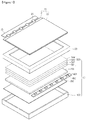
- the liquid crystal display according to the embodiment includes a backlight unit 10 and a liquid crystal panel 20.
- the backlight unit 10 supplies light to the liquid crystal panel 30.
- the backlight unit 10 serves as a surface light source so that the light can be uniformly supplied to a bottom surface of the liquid crystal panel 20.
- the backlight unit 10 is disposed below the liquid crystal panel 20.
- the backlight unit 10 includes a bottom cover 100, a reflective sheet 300, a light source, for example, a plurality of light emitting diodes 400, a printed circuit board 401, a light guide plate 200, and a plurality of optical sheets 500.
- the bottom cover 100 receives the light guide plate 200, the light emitting diodes 400, the printed circuit board 401, the reflective sheet 300, and the optical sheets 500 therein.
- the reflective sheet 201 is disposed below the light guide plate 200.
- the reflective sheet 300 is disposed between the light guide plate 200 and a bottom surface of the bottom cover 100. The reflective sheet 300 reflects the light upward as the light is output downward from the bottom surface of the light guide plate 200.
- the light emitting diodes 400 serve as a light source for generating the light.
- the light emitting diodes 400 are disposed at one side of the light guide plate 200.
- the light generated from the light emitting diodes 400 is incident into the light guide plate 200 through the side of the light guide plate 200.
- the light emitting diodes 400 may include a blue light emitting diode generating the blue light or a UV light emitting diode generating the UV light.
- the light emitting diodes 400 may emit the blue light having the wavelength in the range of about 430nm to about 470nm or the UV light having the a wavelength in the range of about 300nm to abut 400nm.
- the light emitting diodes 400 are mounted on the printed circuit board 401.
- the light emitting diodes 400 may be disposed under the printed circuit board 401.
- the light emitting diodes 400 are driven by receiving a driving signal through the printed circuit board 401.
- the printed circuit board 401 is electrically connected to the light emitting diodes 400.
- the printed circuit board 401 may mount the light emitting diodes 400 thereon.
- the printed circuit board 401 is disposed in the bottom cover 100.
- the light guide plate 200 is disposed in the bottom cover 100.
- the light guide plate 200 is disposed on the reflective sheet 100.
- the light guide plate 200 supplies light received from the light emitting diode 300 upward by reflecting, refracting and scattering the light.
- the light guide plate 200 is disposed below the liquid crystal panel 200.
- the light guide plate 200 is disposed on the reflective sheet 300.
- the light guide plate 200 has a plate shape.
- the light guide plate 200 is transparent.
- a material used for the light guide plate 200 may include an acrylic resin formed by methyl acrylate, ethyl acrylate, cyclohexyl acrylate, or benzene acrylate.
- a guide part 210 may include polymer such as polymethylmethaacrylate ,PMMA, orpolycarbonate, PC.
- the light guide plate 200 may include glass.
- the glass used for the light guide plate 200 may include silicon oxide ,SiO2, titanum oxide TiO2, aluminum hydroxide Al(OH)3 or Zinc oxide ZnO.
- the light guide plate 200 may have a thickness in the range of about 0.5mm to about 1.5mm.
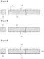
- a plurality of scattering parts 210 is formed on the light guide plate 200. That is, the scattering parts 210 are formed on at least one surface of the light guide plate 200.
- the scattering parts 210 may change a path of incident light. That is, the scattering parts 210 may serve as a light path changing part for changing the path of the incident light. In detail, the scattering parts 210 may scatter the incident light. In more detail, the scattering parts 210 may scatter the incident light upward.
- the scattering parts 210 configure a scattered pattern on a top surface of the light guide plate 200.
- the scattering parts 210 may be disposed on the top surface of the light guide plate 200.
- the scattering parts 210 may include protrusions which are formed on the top surface of the light guide plate 200.
- the scattering parts 210 may have a dot shape when viewed from a top side.
- a diameter R1 of each of scattering parts 210 may be equal to or greater than about 90 ⁇ mThe diameter R1 of each scattering part 210 may be in the range of about 90 ⁇ m to about 300 ⁇ m.In detail, the diameter R1 of each scattering part 210 may be in the range of about 100 ⁇ m to about 300 ⁇ m. In more detail, the diameter R1 of each scattering part 210 may be in the range of about 150 ⁇ m to about 250 ⁇ m.
- the scattering parts 210 are spaced apart from each other. In this case, a pitch P between the scattering parts 210 may be gradually reduced as the scattering parts 210 are located away from the light emitting diodes 400. That is, the scattering parts 210 may be densely disposed as the scattering parts 210 are located away from the light emitting diodes 400. Accordingly, the light guide plate 200 may uniformly supply light upward.
- the scattering part 210 includes a scattering protrusion 211 and a scattering groove 212.
- the scattering protrusion 211 may include a curved surface.
- a protruding part of the scattering protrusion 211 may have a curved surface as a whole.
- the scattering protrusion may have a semisphere shape.
- a diameter R2 of the scattering protrusion 211 may be in the range of about 80 ⁇ m to about 290 ⁇ m.
- a height of the scattering protrusion 211 may be in the range of about 40 ⁇ m to about 150 ⁇ m.
- the scattering groove 212 may be formed on the top surface of the light guide plate 200.
- the scattering groove 212 may be adjacent to the scattering protrusion 211.
- the scattering groove 212 may surround the scattering protrusion 211.
- the scattering groove 212 may extend around the scattering protrusion 211.
- the scattering groove 212 may have a closed loop shape when viewed from the top side.
- a width of each of the grooves 220 may be in the range of about 5 ⁇ m to about 10 ⁇ m.
- a depth of each of the grooves 220 may be in the range of about 2 ⁇ m to about 6 ⁇ m.
- the scattering parts 210 are provided on a bottom surface of the light guide plate 200. That is, the scattering parts 210 may directly face the reflective sheet 300.
- the scattering parts 210 may be provided on both of top and bottom surfaces of the light guide plate 200.
- a plurality of print scattering parts 220 may be provided in the light guide plate 200.
- the print scattering parts 220 may be printed on the top surface and are printed on the bottom surface of the light guide plate 200.
- the print scattering parts 220 may directly provided on the top surface and/or the bottom surface of the light guide plate 200.
- the print scattering parts 220 may be a pattern protruding from at least one surface of the light guide plate 200, for example, the top surface and/or the bottom surface of the light guide plate 200.
- a diameter R3 of each of the print scattering parts 220 is in the range of about 90 ⁇ m to about 300 ⁇ m.
- the diameter R3 of each of the print scattering parts 220 may be in the range of about 100 ⁇ m to about 300 ⁇ m.
- the diameter R3 of each of the print scattering parts 220 may be in the range of about 150 ⁇ m to about 250 ⁇ m.
- the print scattering parts 220 include a plurality of beads 221 and a printing part 222.
- the beads 221 may be transparent.
- the beads 221 may a high refractive index.
- the refractive index of the beads 221 may be in the range of about 1.6 to 2.2.
- the beads 221 include aluminum oxide Al2O3, or titanium oxide, TiO.
- a diameter of each of the beads 221 may be in the range of about 50nm to about 10 ⁇ m. In detail, the diameter of each of the beads 221 may be in the range of about 5 ⁇ m to about 10 ⁇ m.
- the printing part 222 includes a transparent resin.
- the printing part 222 receives the beads 221.
- the beads 221 may be inserted into the printing part 222.
- the printing part 22 may bond the beads 22 to the top surface or the bottom surface of the light guide plate 200.
- the printing part 222 may have a relatively high refractive index.
- a refractive index of the printing part 222 may be in the range of 1.2 to 1.4.
- the print scattering part 220 is farther away from the light emitting diode 400, an area of each printing scattering part 220gradually increases. Accordingly, the print scattering part 220 is farther away from the light emitting diode 400, so reduction in intensity of the light may be compensated.
- the optical sheets 500 are disposed on the light guide plate 200.
- the optical sheets 500 change or improve characteristics of light output from the top surface of the light guide plate 200 to supply the light to the liquid crystal panel 20.
- the optical sheets 500 includes a light conversion sheet 501, a diffusion sheet 502, a first prism sheet 503, and a second prism sheet 504.
- the light conversion sheet 501 is disposed on a light path between the light source and the liquid crystal panel 20.
- the conversion sheet 501 is be on the light guide plate 200.
- the light conversion sheet 501 may be interposed between the light guide plate 200 and the diffusion sheet 502.
- the light conversion sheet 501 may convert wavelength of incident light and supply the converted light upward.
- the light conversion sheet 501 may convert blue light supplied upward from the light guide plate 200 into green light and red light. That is, the light conversion sheet 501 may convert a part of the blue light into green light having a wavelength in the range of about 520nm to about 560nm, and convert another part of the blue light into red light having a wavelength in the range of about 630nm to about 660nm.
- the light conversion sheet 501 may convert UV ray output from the top surface of the light guide plate 200 into blue light, green light, and red light.
- the light conversion sheet 501 may convert a part of the UV ray into blue light having a wavelength in the range of about 430nm to about 470nm, and convert another part of the UV ray into green light having a wavelength in the range of about 520nm to about 560nm, and convert a still another part of the UV ray into red light having a wavelength in the range of about 630nm to about 660nm.
- light passing through the light conversion sheet 510 which is not converted and light converted by the light conversion sheet 501 form white light. That is, the blue light, the green light, and the red light are combined with each other so that the white light may be incident to the liquid crystal panel 20.
- the light conversion sheet 501 includes a lower substrate 510, an upper substrate 520, a light conversion layer 530, a lower reflection preventing layer 540, and an upper reflection preventing layer 550.
- the lower substrate 510 is disposed below the light conversion layer 530.
- the lower substrate 510 may be transparent and flexible.
- the lower substrate 510 may adhere to a bottom surface of the light conversion layer 530.
- a material use for the lower substrate 510 may include transparent polymer such as polyethyleneterephthalate PET.
- the upper substrate 520 is disposed on the light conversion layer 530.
- the upper substrate 520 may be transparent and flexible.
- the upper substrate 520 may adhere to the top surface of the light conversion layer 530.
- a material used for the upper substrate 520 may include transparent polymer such as PET.
- the light conversion layer 530 is sandwiched between the lower substrate 510 and the upper substrate 520.
- the lower substrate 510 and the upper substrate 520 support the light conversion layer 530.
- the lower substrate 510 and the upper substrate 520 protect the light conversion layer 530 from external physical impact.
- the lower substrate 510 and the upper substrate 520 have low oxygen permeability and low moisture permeability.
- the lower substrate 510 and the upper substrate 520 can protect the light conversion layer 530 from external chemical impact by moisture and/or oxygen.
- the light conversion layer 530 is interposed between the lower and upper substrates 510 and 520.
- the light conversion layer 530 may adhere to the top surface of the lower substrate 510, and adhere to the bottom surface of the upper substrate 520.
- the light conversion layer 530 includes a plurality of light conversion particles 531 and a host layer 532.
- the light conversion particles 531 are interposed between the lower and upper substrates 510 and 520.
- the light conversion particles 531 are uniformly distributed in the host layer 532, and the host layer 532 is interposed between the lower substrate 510 and the upper substrate 520.
- the light conversion particles 531 convert a wavelength of the light emitted from the light emitting diodes 400.
- the light conversion particles 531 receive light emitted from the light emitting diodes 400 to convert the a wavelength of the incident light.
- the light conversion particles 531 may convert the blue light emitted from the light emitting diodes 400 into the green light and the red light. That is, a part of the light conversion particles 531 may convert the blue light into green light having a wavelength in the range of about 520nm to about 560nm, and another part of the light conversion particles 531 may convert the blue light into red light having a wavelength in the range of about 630nm to about 660nm.
- the light conversion particles 531 may convert the UV ray emitted from the light emitting diodes 400 into the blue light, the green light, and the red light. That is, a part of the light conversion particles 531 may convert the UV ray into blue light having a wavelength in the range of about 430nm to about 470nm, and another part of the light conversion particles 531 may convert the UV ray into green light having a wavelength in the range of about 520nm to about 560nm. Still another part of the light conversion particles 531 may convert the UV ray into red light having a wavelength in the range of about 630nm to about 660nm.
- light conversion particles 531 for converting the blue light into green light and red light respectively may be used.
- light conversion particles 531 for converting the UV ray into blue light, green light, and red light respectively may be used.
- the light conversion particles 531 are a plurality of quantum dots, QD.
- the quantum dots may include core nano-crystals and shell nano-crystals surrounding the core nano-crystals.
- the quantum dots may include organic ligands bonded to the shell nano-crystals.
- the quantum dots may include an organic coating layer surrounding the shell nano-crystals.
- the shell nano-crystals may be prepared as at least two layers.
- the shell nano-crystals are formed on the surface of the core nano-crystals.
- the quantum dots lengthen a wavelength of the light incident into the core nano-crystals by using the shell nano-crystals forming a shell layer, thereby improving the light efficiency.
- the quantum dots may include at least one of a group-II compound semiconductor, a group-III compound semiconductor, a group-V compound semiconductor, and a group-VI compound semiconductor.
- the core nano-crystals may include CdSe, InGaP, CdTe, CdS, ZnSe, ZnTe, ZnS, HgTe or HgS.
- the shell nano-crystals may include CuZnS, CdSe, CdTe, CdS, ZnSe, ZnTe, ZnS, HgTe or HgS.
- the quantum dot may have a diameter of about 1nm to about 10nm.
- the wavelength of the light emitted from the quantum dots can be adjusted according to the size of the quantum dots.
- the organic ligand may include pyridine, mercapto alcohol, thiol, phosphine and phosphine oxide.
- the organic ligand may stabilize the unstable quantum dots after the synthesis process. Dangling bonds may be formed at the valence band and the quantum dots may be unstable due to the dangling bonds. However, since one end of the organic ligand is the non-bonding state, the one end of the organic ligand is bonded with the dangling bonds, thereby stabilizing the quantum dots.
- the size of the quantum dot is smaller than the Bohr radius of an exciton, which consists of an electron and a hole excited by light and electricity, the quantum confinement effect may occur, so that the quantum dot may have the discrete energy level.
- the size of the energy gap is changed.
- the charges are confined within the quantum dot, so that the light emitting efficiency can be improved.
- the fluorescent a wavelength of the quantum dot may vary depending on the size of the particles.
- the light has the shorter a wavelength as the size of the particle is reduced, so that the fluorescent light having the wavelength band of visible ray can be generated by adjusting the size of the particles.
- the quantum dot represents the extinction coefficient which is 100 to 1000 times higher than that of the general pigment and has the superior quantum yield as compared with the general pigment, so that strong fluorescent light can be generated.
- the quantum dots can be synthesized through the chemical wet scheme.
- the chemical wet scheme is to grow the particles by immersing the precursor material in the organic solvent. According to the chemical wet scheme, the quantum dots can be synthesized.
- the host layer 532 surrounds the light conversion particles 531. That is, the light conversion particles 531 are uniformly distributed in the host layer 532.
- the host layer 531 may include a polymer.
- the host layer 532 is transparent. That is, the host layer 532 may be formed by using a transparent polymer.
- the host layer 532 is interposed between the lower and upper substrates 510 and 520.
- the host layer 532 may adhere to the top surface of the lower substrate 510 and the bottom surface of the upper substrate 520.
- the sealing part 540 is disposed at the side of the light conversion layer 530.
- the sealing part 540 covers the side of the light conversion layer 530.
- the sealing part 540 can also be disposed at the sides of the lower substrate 510 and the upper substrate 520. In this case, the sealing part 540 covers the sides of the lower substrate 510 and the upper substrate 520.
- sealing part 540 may be bonded to the sides of the light conversion layer 530, the lower substrate 510 and the upper substrate 520. In addition, the sealing part 540 may closely adhere to the sides of the light conversion layer 530, the lower substrate 510 and the upper substrate 520.
- the sealing part 540 can seal the side of the wavelength conversion layer 530. That is, the sealing part 540 may serve as a protective part for protecting the wavelength conversion layer 530 from the external chemical impact.
- the liquid crystal panel 20 is disposed on the optical sheets 500.
- the liquid crystal panel 20 is disposed on the panel guide 23.
- the liquid crystal panel 20 may be guided by the panel guide 23.
- the liquid crystal panel 20 displays images by adjusting intensity of light passing through the liquid crystal panel 20.
- the liquid crystal panel 20 is a display panel for displaying the images by using the light emitted from the backlight unit 10.
- the liquid crystal panel 20 includes a TFT substrate 21, a color filter substrate 22 and a liquid crystal layer interposed between the two substrates.
- the liquid crystal panel 20 includes polarizing filters.
- the TFT substrate 21 includes a plurality of gate lines and a plurality of data lines crossing the gate lines to define pixels and a thin film transistor, TFT, is provided at each cross section such that the thin film transistor TFT can be connected to a pixel electrode of the pixel in one-to-one correspondence.
- the color filter substrate 22 includes color filters having R, G and B colors corresponding to the pixels, a black matrix covering the gate lines, data lines and thin film transistors within the limit of the color filters, and a common electrode covering the above elements.
- a driving PCB 25 is provided at an outer peripheral portion of the liquid crystal panel 210 to supply driving signals to the gate lines and data lines.
- the driving PCB 25 is electrically connected to the liquid crystal panel 20 by a COF (chip on film) 24.
- the COF 24 may be replaced with a TCP (tape carrier package).
- the liquid crystal display according to the embodiment disposes the light conversion member on the light guide plate 200 and the scattering parts 210 have a large diameter in the range of about 90 ⁇ m to about 300 ⁇ m.
- the light conversion member includes the light conversion particles.
- the light conversion particles may randomly change a light path while convert a wavelength of incident light. That is, the light conversion particles may also perform a scattering function.
- the scattering parts 210 have a large diameter, because the light conversion member has the scattering function, the whole brightness uniformity is not reduced.
- the scattering parts 210 have a large diameter so that the whole brightness may be increased.
- the display device can represent improved brightness without reducing brightness uniformity.
- any reference in this specification to "one embodiment,” “an embodiment,” “example embodiment,” etc. means that a particular feature, structure, or characteristic described in connection with the embodiment is included in at least one embodiment of the invention.
- the appearances of such phrases in various places in the specification are not necessarily all referring to the same embodiment.
- a light conversion sheet including a CdSe/ZnS quantum dot having a diameter of about 2nm was disposed on a top surface of a light guide plate in which scattering parts having a diameter of about 150 ⁇ m were provided, and then light was emitted to a side of the light guide plate using a blue light emitting diode.
- Comparative Example is similar to Experimental Example except that the scattering parts having a diameter of about 25 ⁇ m were provided on the light guide plate.
- Brightness uniformity of the Experimental Example is substantially the same as that of the Comparative Example and brightness of the Experimental Example was improved by about 2% as compared with that of the Comparative Example.
Landscapes
- Physics & Mathematics (AREA)
- General Physics & Mathematics (AREA)
- Optics & Photonics (AREA)
- Nonlinear Science (AREA)
- Mathematical Physics (AREA)
- Chemical & Material Sciences (AREA)
- Crystallography & Structural Chemistry (AREA)
- Planar Illumination Modules (AREA)
Description
- The embodiment relates to an optical member and a display device having the same.
- Recently, flat display devices, such as an LCD (liquid crystal display), a PDA (plasma display panel) or an OLED (organic light emitting diode), have been increasingly developed instead of conventional CRTs (cathode ray tubes).
- Among them, the LCD includes a liquid crystal display panel having a thin film transistor substrate, a color filter substrate and a liquid crystal injected between the thin film transistor substrate and the color filter substrate. Since the liquid crystal display panel is a non-emissive device, a backlight unit is provided below the thin film transistor substrate to supply light. Transmittance of the light emitted from the backlight unit is adjusted according to the alignment state of the liquid crystal.
- The backlight unit is classified into an edge-illumination type backlight unit and a direct-illumination type backlight unit according to the position of a light source. According to the edge-illumination type backlight unit, the light source is located at a side of a light guide plate.
- The direct-illumination type backlight unit has been developed as the size of the LCD has become enlarged. According to the direct-illumination type backlight unit, at least one light source is located below the liquid crystal display panel to supply the light over the whole area of the liquid crystal display panel.
- When comparing with the edge-illumination type backlight unit, the direct-illumination type backlight unit can employ a large number of light sources so that the high brightness can be achieved. In contrast, the direct-illumination type backlight unit must have thickness larger than thickness of the edge-illumination type backlight unit in order to ensure brightness uniformity.
- In order to solve the above problem, a quantum dot bar having a plurality of quantum dots, which can convert blue light into red light or green light, is positioned in front of a blue LED that emits the blue light. Thus, as the blue light is irradiated onto the quantum dot bar, the blue light, the red light and the green light are mixed with each other by the quantum dots distributed in the quantum dot bar and the mixed light is incident into the light guide plate, so that white light is generated.
- If the white light is supplied to the light guide plate by using the quantum dot bar, high color reproduction may be realized.
- The backlight unit may include an FPCB (flexible printed circuit board) provided at one side of the blue LED, which generates blue light, to supply signals and power to the LED and a bonding member formed under the bottom surface of the FPCB.
- The display device capable of displaying various images using the white light supplied to the light guide plate through the quantum dot bar as the blue light is emitted from the blue LED has been extensively used.
- The display device employing the quantum dots is disclosed in
Korean Unexamined Patent Publication No. 10-2011-0068110 -
KR 100 943 233 B1US 2009/034230 A1 , andWO 01/66997 A2 - The embodiment provides a display device representing improved brightness.
- According to the embodiment, there is provided a display device according to claim 1.
-
-
FIG. 1 is an exploded perspective view showing a liquid crystal display according to the embodiment; -
FIG. 2 is a perspective view showing a light guide plate; -
FIG. 3 is a sectional view taken along line A-A' ofFIG. 2 ; -
FIG. 4 is a sectional view showing the light guide plate; -
FIG. 5 is a sectional view showing a light guide plate; -
FIG. 6 is a sectional view showing a light guide plate; -
FIG. 7 is a perspective view showing the light guide plate; -
FIG. 8 is a sectional view taken along line B-B' ofFIG. 7 ; -
FIG. 9 is a perspective view showing a light conversion sheet; -
FIG. 10 is a sectional view taken along line C-C' ofFIG. 9 . - In the description of the embodiments, it will be understood that, when a substrate, a frame, a sheet, a layer, or a pattern is referred to as being "on" or "under" another substrate, another frame, another sheet, another layer, or another pattern, it can be "directly" or "indirectly" on the other substrate, frame, sheet, layer, or pattern, one or more intervening layers may also be present. Such a position of each element has been described with reference to the drawings. The thickness and size of each element shown in the drawings may be exaggerated, omitted or schematically drawn for the purpose of convenience or clarity. In addition, the size of elements does not utterly reflect an actual size.
-
FIG. 1 is an exploded perspective view showing a liquid crystal display according to the embodiment.FIG. 2 is a perspective view showing a light guide plate.FIG. 3 is a sectional view taken along line A-A' ofFIG. 2 .FIG. 4 is a sectional view showing the light guide plate.FIG. 5 is a sectional view showing another light guide plate.FIG. 6 is a sectional view showing another light guide plate.FIG. 7 is a perspective view showing the light guide plate.FIG. 8 is a sectional view taken along line B-B' ofFIG. 7 .FIG. 9 is a perspective view showing a light conversion 2. sheet.FIG. 10 is a sectional view taken along line C-C' ofFIG. 9 . - Referring to
FIGS. 1 to 10 , the liquid crystal display according to the embodiment includes abacklight unit 10 and aliquid crystal panel 20. - The
backlight unit 10 supplies light to the liquid crystal panel 30. Thebacklight unit 10 serves as a surface light source so that the light can be uniformly supplied to a bottom surface of theliquid crystal panel 20. - The
backlight unit 10 is disposed below theliquid crystal panel 20. Thebacklight unit 10 includes abottom cover 100, areflective sheet 300, a light source, for example, a plurality oflight emitting diodes 400, aprinted circuit board 401, alight guide plate 200, and a plurality ofoptical sheets 500. - An upper portion of the
bottom cover 100 is open. Thebottom cover 100 receives thelight guide plate 200, thelight emitting diodes 400, the printedcircuit board 401, thereflective sheet 300, and theoptical sheets 500 therein. - The reflective sheet 201 is disposed below the
light guide plate 200. In more detail, thereflective sheet 300 is disposed between thelight guide plate 200 and a bottom surface of thebottom cover 100. Thereflective sheet 300 reflects the light upward as the light is output downward from the bottom surface of thelight guide plate 200. - The
light emitting diodes 400 serve as a light source for generating the light. Thelight emitting diodes 400 are disposed at one side of thelight guide plate 200. The light generated from thelight emitting diodes 400 is incident into thelight guide plate 200 through the side of thelight guide plate 200. - The
light emitting diodes 400 may include a blue light emitting diode generating the blue light or a UV light emitting diode generating the UV light. In detail, thelight emitting diodes 400 may emit the blue light having the wavelength in the range of about 430nm to about 470nm or the UV light having the a wavelength in the range of about 300nm to abut 400nm. - The
light emitting diodes 400 are mounted on the printedcircuit board 401. Thelight emitting diodes 400 may be disposed under the printedcircuit board 401. Thelight emitting diodes 400 are driven by receiving a driving signal through the printedcircuit board 401. - The printed
circuit board 401 is electrically connected to thelight emitting diodes 400. The printedcircuit board 401 may mount thelight emitting diodes 400 thereon. The printedcircuit board 401 is disposed in thebottom cover 100. - The
light guide plate 200 is disposed in thebottom cover 100. Thelight guide plate 200 is disposed on thereflective sheet 100. Thelight guide plate 200 supplies light received from thelight emitting diode 300 upward by reflecting, refracting and scattering the light. - The
light guide plate 200 is disposed below theliquid crystal panel 200. Thelight guide plate 200 is disposed on thereflective sheet 300. Thelight guide plate 200 has a plate shape. Thelight guide plate 200 is transparent. For example, a material used for thelight guide plate 200 may include an acrylic resin formed by methyl acrylate, ethyl acrylate, cyclohexyl acrylate, or benzene acrylate. For example, aguide part 210 may include polymer such as polymethylmethaacrylate ,PMMA, orpolycarbonate, PC. Thelight guide plate 200 may include glass. In detail, the glass used for thelight guide plate 200 may include silicon oxide ,SiO2, titanum oxide TiO2, aluminum hydroxide Al(OH)3 or Zinc oxide ZnO. Thelight guide plate 200 may have a thickness in the range of about 0.5mm to about 1.5mm. - As shown in
FIGS. 2 to 4 , a plurality of scatteringparts 210 is formed on thelight guide plate 200. That is, the scatteringparts 210 are formed on at least one surface of thelight guide plate 200. The scatteringparts 210 may change a path of incident light. That is, the scatteringparts 210 may serve as a light path changing part for changing the path of the incident light. In detail, the scatteringparts 210 may scatter the incident light. In more detail, the scatteringparts 210 may scatter the incident light upward. The scatteringparts 210 configure a scattered pattern on a top surface of thelight guide plate 200. - The scattering
parts 210 may be disposed on the top surface of thelight guide plate 200. The scatteringparts 210 may include protrusions which are formed on the top surface of thelight guide plate 200. The scatteringparts 210 may have a dot shape when viewed from a top side. - A diameter R1 of each of scattering
parts 210 may be equal to or greater than about 90µmThe diameter R1 of each scatteringpart 210 may be in the range of about 90µm to about 300µm.In detail, the diameter R1 of each scatteringpart 210 may be in the range of about 100µm to about 300µm. In more detail, the diameter R1 of each scatteringpart 210 may be in the range of about 150µm to about 250µm. - The scattering
parts 210 are spaced apart from each other. In this case, a pitch P between the scatteringparts 210 may be gradually reduced as the scatteringparts 210 are located away from thelight emitting diodes 400. That is, the scatteringparts 210 may be densely disposed as the scatteringparts 210 are located away from thelight emitting diodes 400. Accordingly, thelight guide plate 200 may uniformly supply light upward. - The
scattering part 210 includes ascattering protrusion 211 and ascattering groove 212. - The scattering
protrusion 211 may include a curved surface. A protruding part of thescattering protrusion 211 may have a curved surface as a whole. In detail, the scattering protrusion may have a semisphere shape. A diameter R2 of thescattering protrusion 211 may be in the range of about 80µm to about 290µm. A height of thescattering protrusion 211 may be in the range of about 40µm to about 150µm. - The scattering
groove 212 may be formed on the top surface of thelight guide plate 200. The scatteringgroove 212 may be adjacent to thescattering protrusion 211. In detail, the scatteringgroove 212 may surround thescattering protrusion 211. The scatteringgroove 212 may extend around the scatteringprotrusion 211. The scatteringgroove 212 may have a closed loop shape when viewed from the top side. - A width of each of the
grooves 220 may be in the range of about 5µm to about 10µm. A depth of each of thegrooves 220 may be in the range of about 2µm to about 6µm. - As shown in
FIG. 5 , the scatteringparts 210 are provided on a bottom surface of thelight guide plate 200. That is, the scatteringparts 210 may directly face thereflective sheet 300. - As shown in
FIG. 6 , the scatteringparts 210 may be provided on both of top and bottom surfaces of thelight guide plate 200. - As shown in
FIGS. 7 and 8 , a plurality ofprint scattering parts 220 may be provided in thelight guide plate 200. Theprint scattering parts 220 may be printed on the top surface and are printed on the bottom surface of thelight guide plate 200. - The
print scattering parts 220 may directly provided on the top surface and/or the bottom surface of thelight guide plate 200. Theprint scattering parts 220 may be a pattern protruding from at least one surface of thelight guide plate 200, for example, the top surface and/or the bottom surface of thelight guide plate 200. A diameter R3 of each of theprint scattering parts 220 is in the range of about 90µm to about 300µm. In detail, the diameter R3 of each of theprint scattering parts 220 may be in the range of about 100µm to about 300µm. In more detail, the diameter R3 of each of theprint scattering parts 220 may be in the range of about 150µm to about 250µm. - The
print scattering parts 220 include a plurality ofbeads 221 and aprinting part 222. Thebeads 221 may be transparent. Thebeads 221 may a high refractive index. The refractive index of thebeads 221 may be in the range of about 1.6 to 2.2. Thebeads 221 include aluminum oxide Al2O3, or titanium oxide, TiO. - A diameter of each of the
beads 221 may be in the range of about 50nm to about 10µm. In detail, the diameter of each of thebeads 221 may be in the range of about 5µm to about 10µm. - The
printing part 222 includes a transparent resin. Theprinting part 222 receives thebeads 221. Thebeads 221 may be inserted into theprinting part 222. Theprinting part 22 may bond thebeads 22 to the top surface or the bottom surface of thelight guide plate 200. Theprinting part 222 may have a relatively high refractive index. A refractive index of theprinting part 222 may be in the range of 1.2 to 1.4. - If the
print scattering part 220 is farther away from thelight emitting diode 400, an area of each printing scattering part 220gradually increases. Accordingly, theprint scattering part 220 is farther away from thelight emitting diode 400, so reduction in intensity of the light may be compensated. - The
optical sheets 500 are disposed on thelight guide plate 200. Theoptical sheets 500 change or improve characteristics of light output from the top surface of thelight guide plate 200 to supply the light to theliquid crystal panel 20. - The
optical sheets 500 includes alight conversion sheet 501, adiffusion sheet 502, afirst prism sheet 503, and asecond prism sheet 504. - The
light conversion sheet 501 is disposed on a light path between the light source and theliquid crystal panel 20. Theconversion sheet 501 is be on thelight guide plate 200. In detail, thelight conversion sheet 501 may be interposed between thelight guide plate 200 and thediffusion sheet 502. Thelight conversion sheet 501 may convert wavelength of incident light and supply the converted light upward. - For example, when the
light emitting diodes 400 are blue light emitting diodes, thelight conversion sheet 501 may convert blue light supplied upward from thelight guide plate 200 into green light and red light. That is, thelight conversion sheet 501 may convert a part of the blue light into green light having a wavelength in the range of about 520nm to about 560nm, and convert another part of the blue light into red light having a wavelength in the range of about 630nm to about 660nm. - When the
light emitting diodes 400 are UV light emitting diodes, thelight conversion sheet 501 may convert UV ray output from the top surface of thelight guide plate 200 into blue light, green light, and red light. Thelight conversion sheet 501 may convert a part of the UV ray into blue light having a wavelength in the range of about 430nm to about 470nm, and convert another part of the UV ray into green light having a wavelength in the range of about 520nm to about 560nm, and convert a still another part of the UV ray into red light having a wavelength in the range of about 630nm to about 660nm. - Accordingly, light passing through the
light conversion sheet 510 which is not converted and light converted by thelight conversion sheet 501 form white light. That is, the blue light, the green light, and the red light are combined with each other so that the white light may be incident to theliquid crystal panel 20. - As shown in
FIGS. 9 and 10 , thelight conversion sheet 501 includes alower substrate 510, anupper substrate 520, alight conversion layer 530, a lowerreflection preventing layer 540, and an upper reflection preventing layer 550. - The
lower substrate 510 is disposed below thelight conversion layer 530. Thelower substrate 510 may be transparent and flexible. Thelower substrate 510 may adhere to a bottom surface of thelight conversion layer 530. - For example, a material use for the
lower substrate 510 may include transparent polymer such as polyethyleneterephthalate PET. - The
upper substrate 520 is disposed on thelight conversion layer 530. Theupper substrate 520 may be transparent and flexible. Theupper substrate 520 may adhere to the top surface of thelight conversion layer 530. - For example, a material used for the
upper substrate 520 may include transparent polymer such as PET. - The
light conversion layer 530 is sandwiched between thelower substrate 510 and theupper substrate 520. Thelower substrate 510 and theupper substrate 520 support thelight conversion layer 530. Thelower substrate 510 and theupper substrate 520 protect thelight conversion layer 530 from external physical impact. - The
lower substrate 510 and theupper substrate 520 have low oxygen permeability and low moisture permeability. Thus, thelower substrate 510 and theupper substrate 520 can protect thelight conversion layer 530 from external chemical impact by moisture and/or oxygen. - The
light conversion layer 530 is interposed between the lower andupper substrates light conversion layer 530 may adhere to the top surface of thelower substrate 510, and adhere to the bottom surface of theupper substrate 520. - The
light conversion layer 530 includes a plurality oflight conversion particles 531 and ahost layer 532. - The
light conversion particles 531 are interposed between the lower andupper substrates light conversion particles 531 are uniformly distributed in thehost layer 532, and thehost layer 532 is interposed between thelower substrate 510 and theupper substrate 520. - The
light conversion particles 531 convert a wavelength of the light emitted from thelight emitting diodes 400. In detail, thelight conversion particles 531 receive light emitted from thelight emitting diodes 400 to convert the a wavelength of the incident light. For instance, thelight conversion particles 531 may convert the blue light emitted from thelight emitting diodes 400 into the green light and the red light. That is, a part of thelight conversion particles 531 may convert the blue light into green light having a wavelength in the range of about 520nm to about 560nm, and another part of thelight conversion particles 531 may convert the blue light into red light having a wavelength in the range of about 630nm to about 660nm. - In addition, the
light conversion particles 531 may convert the UV ray emitted from thelight emitting diodes 400 into the blue light, the green light, and the red light. That is, a part of thelight conversion particles 531 may convert the UV ray into blue light having a wavelength in the range of about 430nm to about 470nm, and another part of thelight conversion particles 531 may convert the UV ray into green light having a wavelength in the range of about 520nm to about 560nm. Still another part of thelight conversion particles 531 may convert the UV ray into red light having a wavelength in the range of about 630nm to about 660nm. - That is, when the
light emitting diodes 400 are a bluelight emitting diode 400 for generating blue light,light conversion particles 531 for converting the blue light into green light and red light, respectively may be used. In addition, when thelight emitting diodes 400 are a bluelight emitting diode 400 for generating the UV ray,light conversion particles 531 for converting the UV ray into blue light, green light, and red light, respectively may be used. - The
light conversion particles 531 are a plurality of quantum dots, QD. The quantum dots may include core nano-crystals and shell nano-crystals surrounding the core nano-crystals. In addition, the quantum dots may include organic ligands bonded to the shell nano-crystals. Further, the quantum dots may include an organic coating layer surrounding the shell nano-crystals. - The shell nano-crystals may be prepared as at least two layers. The shell nano-crystals are formed on the surface of the core nano-crystals. The quantum dots lengthen a wavelength of the light incident into the core nano-crystals by using the shell nano-crystals forming a shell layer, thereby improving the light efficiency.
- The quantum dots may include at least one of a group-II compound semiconductor, a group-III compound semiconductor, a group-V compound semiconductor, and a group-VI compound semiconductor. In more detail, the core nano-crystals may include CdSe, InGaP, CdTe, CdS, ZnSe, ZnTe, ZnS, HgTe or HgS. In addition, the shell nano-crystals may include CuZnS, CdSe, CdTe, CdS, ZnSe, ZnTe, ZnS, HgTe or HgS. The quantum dot may have a diameter of about 1nm to about 10nm.
- The wavelength of the light emitted from the quantum dots can be adjusted according to the size of the quantum dots. The organic ligand may include pyridine, mercapto alcohol, thiol, phosphine and phosphine oxide. The organic ligand may stabilize the unstable quantum dots after the synthesis process. Dangling bonds may be formed at the valence band and the quantum dots may be unstable due to the dangling bonds. However, since one end of the organic ligand is the non-bonding state, the one end of the organic ligand is bonded with the dangling bonds, thereby stabilizing the quantum dots.
- In particular, if the size of the quantum dot is smaller than the Bohr radius of an exciton, which consists of an electron and a hole excited by light and electricity, the quantum confinement effect may occur, so that the quantum dot may have the discrete energy level. Thus, the size of the energy gap is changed. In addition, the charges are confined within the quantum dot, so that the light emitting efficiency can be improved.
- Different from general fluorescent pigments, the fluorescent a wavelength of the quantum dot may vary depending on the size of the particles. In detail, the light has the shorter a wavelength as the size of the particle is reduced, so that the fluorescent light having the wavelength band of visible ray can be generated by adjusting the size of the particles. In addition, the quantum dot represents the extinction coefficient which is 100 to 1000 times higher than that of the general pigment and has the superior quantum yield as compared with the general pigment, so that strong fluorescent light can be generated.
- The quantum dots can be synthesized through the chemical wet scheme. The chemical wet scheme is to grow the particles by immersing the precursor material in the organic solvent. According to the chemical wet scheme, the quantum dots can be synthesized.
- The
host layer 532 surrounds thelight conversion particles 531. That is, thelight conversion particles 531 are uniformly distributed in thehost layer 532. Thehost layer 531 may include a polymer. Thehost layer 532 is transparent. That is, thehost layer 532 may be formed by using a transparent polymer. - The
host layer 532 is interposed between the lower andupper substrates host layer 532 may adhere to the top surface of thelower substrate 510 and the bottom surface of theupper substrate 520. - The sealing
part 540 is disposed at the side of thelight conversion layer 530. In detail, the sealingpart 540 covers the side of thelight conversion layer 530. In more detail, the sealingpart 540 can also be disposed at the sides of thelower substrate 510 and theupper substrate 520. In this case, the sealingpart 540 covers the sides of thelower substrate 510 and theupper substrate 520. - In addition, the sealing
part 540 may be bonded to the sides of thelight conversion layer 530, thelower substrate 510 and theupper substrate 520. In addition, the sealingpart 540 may closely adhere to the sides of thelight conversion layer 530, thelower substrate 510 and theupper substrate 520. - Therefore, the sealing
part 540 can seal the side of thewavelength conversion layer 530. That is, the sealingpart 540 may serve as a protective part for protecting thewavelength conversion layer 530 from the external chemical impact. - The
liquid crystal panel 20 is disposed on theoptical sheets 500. In addition, theliquid crystal panel 20 is disposed on thepanel guide 23. Theliquid crystal panel 20 may be guided by thepanel guide 23. - The
liquid crystal panel 20 displays images by adjusting intensity of light passing through theliquid crystal panel 20. In detail, theliquid crystal panel 20 is a display panel for displaying the images by using the light emitted from thebacklight unit 10. Theliquid crystal panel 20 includes aTFT substrate 21, acolor filter substrate 22 and a liquid crystal layer interposed between the two substrates. In addition, theliquid crystal panel 20 includes polarizing filters. - Hereinafter, the
TFT substrate 21 and thecolor filter substrate 22 will be described in detail although they are not shown in the drawings in detail. TheTFT substrate 21 includes a plurality of gate lines and a plurality of data lines crossing the gate lines to define pixels and a thin film transistor, TFT, is provided at each cross section such that the thin film transistor TFT can be connected to a pixel electrode of the pixel in one-to-one correspondence. Thecolor filter substrate 22 includes color filters having R, G and B colors corresponding to the pixels, a black matrix covering the gate lines, data lines and thin film transistors within the limit of the color filters, and a common electrode covering the above elements. - A driving
PCB 25 is provided at an outer peripheral portion of theliquid crystal panel 210 to supply driving signals to the gate lines and data lines. - The driving
PCB 25 is electrically connected to theliquid crystal panel 20 by a COF (chip on film) 24. TheCOF 24 may be replaced with a TCP (tape carrier package). - As described above, the liquid crystal display according to the embodiment disposes the light conversion member on the
light guide plate 200 and the scatteringparts 210 have a large diameter in the range of about 90µm to about 300µm.In this case, the light conversion member includes the light conversion particles. The light conversion particles may randomly change a light path while convert a wavelength of incident light. That is, the light conversion particles may also perform a scattering function. - Accordingly, even if the scattering
parts 210 have a large diameter, because the light conversion member has the scattering function, the whole brightness uniformity is not reduced. - Therefore, the scattering
parts 210 have a large diameter so that the whole brightness may be increased. - As a result, the display device according to the embodiment can represent improved brightness without reducing brightness uniformity.
- Any reference in this specification to "one embodiment," "an embodiment," "example embodiment," etc., means that a particular feature, structure, or characteristic described in connection with the embodiment is included in at least one embodiment of the invention. The appearances of such phrases in various places in the specification are not necessarily all referring to the same embodiment. Further, when a particular feature, structure, or characteristic is described in connection with any embodiment, it is submitted that it is within the purview of one skilled in the art to effect such feature, structure, or characteristic in connection with other ones of the embodiments.
- A light conversion sheet including a CdSe/ZnS quantum dot having a diameter of about 2nm was disposed on a top surface of a light guide plate in which scattering parts having a diameter of about 150µm were provided, and then light was emitted to a side of the light guide plate using a blue light emitting diode.
- Comparative Example is similar to Experimental Example except that the scattering parts having a diameter of about 25µm were provided on the light guide plate.
- Brightness uniformity of the Experimental Example is substantially the same as that of the Comparative Example and brightness of the Experimental Example was improved by about 2% as compared with that of the Comparative Example.
Claims (8)
- A display device comprising:a light guide plate (200) having an upper surface, a bottom surface and side surfaces;a light source including a plurality of light emitting diodes (400) and being provided laterally to the light guide plate (200) to emit light into at least one side surface of the light guide plate (200);a light conversion member (501) on the light guide plate (200);a reflective sheet (300) under the light guide plate (200);a display panel (20) on the light conversion member; anda plurality of print scattering parts (220) on the bottom surface of the light guide plate (200),wherein the light guide plate (200) is provided between the light conversion member and the reflective sheet,wherein the print scattering parts (220) provided between the bottom surface of the light guide plate (200) and the reflective sheet,characterized in that each of the plurality of print scattering parts (220) has a diameter in a range of 90µm to 300µm, and
wherein the light conversion member (501) comprises:a lower substrate (510);a light conversion layer (530) on the lower substrate (510); andan upper substrate (520) on the light conversion layer,wherein the light conversion layer (530) comprises:a host layer (532); anda plurality of quantum dots (531) dispersed in the host layer (532),wherein each of the printing scattering part comprise a plurality of beads, and resin which receives the beads,wherein the beads include aluminum oxide, Al2O3, or titanium oxide ,TiO, and wherein further an area of each of the plurality of the scattering parts gradually increases as its distance from the light emitting diodes increases. - The display device of claim 1, wherein the beads are in directly contact with the resin of the each scattering part
- The display device of claim 1, further comprising print scattering parts provided on the top surface of the light guide plate (200).
- The display device of claim 3, wherein the upper scattering parts include a plurality of beads.
- The display device of claim 4, wherein a diameter of each the beads of the upper scattering parts are in the range 50nm to 10µm.
- The display device of claim 1, wherein at least one of the lower substrate and the upper substrate comprise polyethyleneterephthalate, PET.
- The display device of claim 1, wherein the light conversion member further comprises at least one of a lower reflection preventing layer and an upper reflection preventing layer.
- The display device of claim 1, wherein a refractive index of the beads and the resin are different.
Applications Claiming Priority (3)
| Application Number | Priority Date | Filing Date | Title |
|---|---|---|---|
| KR1020110131365A KR101664507B1 (en) | 2011-12-08 | 2011-12-08 | Display device |
| PCT/KR2012/009995 WO2013085187A1 (en) | 2011-12-08 | 2012-11-23 | Display device |
| EP12856122.2A EP2788816A4 (en) | 2011-12-08 | 2012-11-23 | DISPLAY DEVICE |
Related Parent Applications (1)
| Application Number | Title | Priority Date | Filing Date |
|---|---|---|---|
| EP12856122.2A Division EP2788816A4 (en) | 2011-12-08 | 2012-11-23 | DISPLAY DEVICE |
Publications (2)
| Publication Number | Publication Date |
|---|---|
| EP3267246A1 EP3267246A1 (en) | 2018-01-10 |
| EP3267246B1 true EP3267246B1 (en) | 2021-09-29 |
Family
ID=48574499
Family Applications (2)
| Application Number | Title | Priority Date | Filing Date |
|---|---|---|---|
| EP17184709.8A Active EP3267246B1 (en) | 2011-12-08 | 2012-11-23 | Display device |
| EP12856122.2A Ceased EP2788816A4 (en) | 2011-12-08 | 2012-11-23 | DISPLAY DEVICE |
Family Applications After (1)
| Application Number | Title | Priority Date | Filing Date |
|---|---|---|---|
| EP12856122.2A Ceased EP2788816A4 (en) | 2011-12-08 | 2012-11-23 | DISPLAY DEVICE |
Country Status (6)
| Country | Link |
|---|---|
| US (2) | US9494723B2 (en) |
| EP (2) | EP3267246B1 (en) |
| KR (1) | KR101664507B1 (en) |
| CN (2) | CN104081264A (en) |
| TW (1) | TWI588548B (en) |
| WO (1) | WO2013085187A1 (en) |
Families Citing this family (18)
| Publication number | Priority date | Publication date | Assignee | Title |
|---|---|---|---|---|
| JP6002071B2 (en) * | 2013-03-26 | 2016-10-05 | 株式会社東芝 | Illumination device and light guide member |
| JP2015046328A (en) * | 2013-08-28 | 2015-03-12 | 富士フイルム株式会社 | Light guide plate, backlight unit and liquid crystal display device including the same, and optical sheet |
| KR20150064463A (en) | 2013-12-03 | 2015-06-11 | 삼성디스플레이 주식회사 | Light emitting diode package and display device having the same as light source |
| TWI518386B (en) * | 2014-04-02 | 2016-01-21 | 群創光電股份有限公司 | Display device |
| JP5843024B1 (en) | 2014-08-22 | 2016-01-13 | 大日本印刷株式会社 | Display device |
| JP6746498B2 (en) | 2014-08-22 | 2020-08-26 | Nsマテリアルズ株式会社 | Wavelength conversion member, light emitting device using the same, light emitting element, light source device, and display device |
| CN107209418A (en) * | 2015-01-06 | 2017-09-26 | 康宁公司 | Electrodeless OLED lighting devices and the LCD system using described device |
| WO2016130731A1 (en) * | 2015-02-13 | 2016-08-18 | Corning Incorporated | Angular filters and display devices comprising the same |
| KR102312522B1 (en) * | 2015-06-11 | 2021-10-15 | 삼성디스플레이 주식회사 | Display device |
| KR101608963B1 (en) * | 2015-06-19 | 2016-04-04 | (주)코이즈 | Light guide plate having complex pattern and method of manufacturing the same |
| KR20170004205A (en) * | 2015-07-01 | 2017-01-11 | 엘지전자 주식회사 | Light guide plate and plane light source device having the same |
| KR102527931B1 (en) * | 2016-08-02 | 2023-05-03 | 삼성디스플레이 주식회사 | Back light unit and display device comprising the same |
| CN107065299A (en) * | 2016-12-31 | 2017-08-18 | 惠科股份有限公司 | Method for manufacturing backlight module |
| CN107193077A (en) * | 2017-07-24 | 2017-09-22 | 武汉华星光电技术有限公司 | Backlight module and liquid crystal display |
| US10495923B2 (en) | 2017-07-24 | 2019-12-03 | Wuhan China Star Optoelectronics Technology Co., Ltd. | Backlight module and liquid crystal display |
| KR102436671B1 (en) * | 2018-01-03 | 2022-08-29 | 삼성디스플레이 주식회사 | Backlight unit and display apparatus including the same |
| US20190219874A1 (en) * | 2018-01-16 | 2019-07-18 | Huizhou China Star Optoelectronics Technology Co., Ltd. | Backlight module and display device |
| CN110673244B (en) * | 2019-09-27 | 2021-02-02 | 南京贝迪新材料科技股份有限公司 | Quantum dot composite brightness enhancement film and preparation method thereof |
Family Cites Families (60)
| Publication number | Priority date | Publication date | Assignee | Title |
|---|---|---|---|---|
| CA2401459A1 (en) | 2000-03-06 | 2001-09-13 | Teledyne Lighting And Display Products, Inc. | Lighting apparatus having quantum dot layer |
| CN2496052Y (en) | 2001-04-13 | 2002-06-19 | 宋义 | Improved, uniform and high efficiency side lighting type back light source |
| CN2586980Y (en) | 2002-11-23 | 2003-11-19 | 鸿富锦精密工业(深圳)有限公司 | Back light module |
| CN2588387Y (en) | 2002-12-13 | 2003-11-26 | 鸿富锦精密工业(深圳)有限公司 | Light conducting board and plane illumination device |
| TWI280427B (en) * | 2003-01-29 | 2007-05-01 | Hon Hai Prec Ind Co Ltd | Back light module |
| CN100376950C (en) | 2003-11-13 | 2008-03-26 | 鸿富锦精密工业(深圳)有限公司 | Backlight module and its light guide plate |
| TWI291770B (en) * | 2003-11-14 | 2007-12-21 | Hon Hai Prec Ind Co Ltd | Surface light source device and light emitting diode |
| TWI275858B (en) * | 2003-11-14 | 2007-03-11 | Hon Hai Prec Ind Co Ltd | Light guide plate |
| TWI283777B (en) | 2003-11-14 | 2007-07-11 | Hon Hai Prec Ind Co Ltd | Light guide plate and method for making it and backlight module using it |
| TW200517238A (en) * | 2003-11-21 | 2005-06-01 | Hon Hai Prec Ind Co Ltd | A light guide plate injection mold |
| TW200528849A (en) | 2004-02-27 | 2005-09-01 | Hon Hai Prec Ind Co Ltd | Light guide plate |
| TWI300494B (en) * | 2004-07-23 | 2008-09-01 | Hon Hai Prec Ind Co Ltd | Light guiding plate and backlight module using the same |
| TWI299412B (en) * | 2004-08-27 | 2008-08-01 | Hon Hai Prec Ind Co Ltd | Light guide plate and backlight module using the same |
| TWI276882B (en) * | 2004-12-10 | 2007-03-21 | Hon Hai Prec Ind Co Ltd | Light guide plate and backlight module |
| US7416309B2 (en) * | 2004-12-30 | 2008-08-26 | 3M Innovative Properties Company | Optical film having a surface with rounded structures |
| JP4329736B2 (en) * | 2005-07-04 | 2009-09-09 | セイコーエプソン株式会社 | Optical substrate, planar illumination device, electro-optical device |
| KR20070108794A (en) | 2006-05-08 | 2007-11-13 | 미래나노텍(주) | Back light assembly of the liquid crystal display device provided with the optical sheet and the optical sheet |
| TW200817777A (en) | 2006-08-03 | 2008-04-16 | Harison Toshiba Lighting Corp | Hollow type flat lighting system |
| CN100516642C (en) * | 2006-08-03 | 2009-07-22 | 哈利盛东芝照明株式会社 | Hollow type plate illuminating device |
| US7661862B2 (en) | 2006-12-07 | 2010-02-16 | Skc Haas Display Films Co., Ltd. | LCD display backlight using elongated illuminators |
| US8456590B2 (en) * | 2007-01-09 | 2013-06-04 | Dai Nippon Printing Co., Ltd. | Optical sheet, surface light source and display device |
| TWM322627U (en) | 2007-06-06 | 2007-11-21 | Acpa Energy Conversion Devices | Passive light-emitting module whose visible lights are excited from the ultraviolet |
| CN101349776A (en) | 2007-07-18 | 2009-01-21 | 宣茂科技股份有限公司 | light guide plate |
| US20090034230A1 (en) * | 2007-07-31 | 2009-02-05 | Luminus Devices, Inc. | Illumination assembly including wavelength converting material having spatially varying density |
| US8434909B2 (en) * | 2007-10-09 | 2013-05-07 | Flex Lighting Ii, Llc | Light emitting display with light mixing within a film |
| US8269420B2 (en) * | 2007-10-12 | 2012-09-18 | Sony Corporation | Illuminating device having fluorescent lamp, display apparatus including the same, and light-diffusing film |
| US20090122227A1 (en) | 2007-11-08 | 2009-05-14 | Rohm And Haas Denmark Finance A/S | Integrated backlight illumination assembly |
| KR20100100880A (en) * | 2007-12-17 | 2010-09-15 | 히다치 가세고교 가부시끼가이샤 | Optical waveguide for visible light |
| KR101460155B1 (en) * | 2008-01-15 | 2014-11-10 | 삼성전자주식회사 | Backlight unit and liquid crystal display having the same |
| TWM341811U (en) | 2008-02-18 | 2008-10-01 | Kismart Corp | Light source module with shared wavelength converting structure |
| CN101280190A (en) * | 2008-05-26 | 2008-10-08 | 南开大学 | Method for Synthesizing Stable GSH-CdTeSe Alloy Quantum Dots in Aqueous Phase |
| CN101614839A (en) | 2008-06-26 | 2009-12-30 | 胜华科技股份有限公司 | Backlight module and light guide plate |
| JP5616886B2 (en) * | 2008-07-01 | 2014-10-29 | コーニンクレッカ フィリップス エヌ ヴェ | Light-emitting diode that converts wavelength with little unconverted light emission |
| DE102008031996A1 (en) * | 2008-07-07 | 2010-02-18 | Osram Gesellschaft mit beschränkter Haftung | Radiation-emitting device |
| CN101634726B (en) * | 2008-07-21 | 2012-06-13 | 鸿富锦精密工业(深圳)有限公司 | Light panel and manufacturing method as well as backlight module adopting same |
| CN101685180A (en) | 2008-09-27 | 2010-03-31 | 上海边光实业有限公司 | Light guide plate favourable for even distribution of light |
| JP2010096916A (en) * | 2008-10-15 | 2010-04-30 | Keiwa Inc | Optical sheet and backlight unit using the same |
| TWI410713B (en) | 2008-11-06 | 2013-10-01 | Ind Tech Res Inst | Backlight modules, and liquid crystal display |
| JP2012514071A (en) * | 2008-12-30 | 2012-06-21 | ナノシス・インク. | Method for encapsulating nanocrystals and the resulting composition |
| CN101856684A (en) * | 2009-04-08 | 2010-10-13 | 鸿富锦精密工业(深圳)有限公司 | Lens, lens array and manufacturing method thereof |
| KR20090054415A (en) | 2009-04-24 | 2009-05-29 | 미래나노텍(주) | Back light assembly of the liquid crystal display device provided with the optical sheet and the optical sheet |
| CN101870151A (en) * | 2009-04-27 | 2010-10-27 | 鸿富锦精密工业(深圳)有限公司 | Optical element manufacturing method and imprint mold |
| US8794812B2 (en) * | 2009-05-01 | 2014-08-05 | Abl Ip Holding Llc | Light emitting devices and applications thereof |
| KR100943233B1 (en) * | 2009-06-03 | 2010-02-18 | 주식회사 우즈필 | Diffusion Ink Composition |
| KR20110006811A (en) | 2009-07-15 | 2011-01-21 | 삼성전자주식회사 | Color Filter Arrays and Image Sensors and Electronic Devices Comprising the Same |
| KR20110022970A (en) * | 2009-08-28 | 2011-03-08 | 엘지이노텍 주식회사 | Display |
| JPWO2011067911A1 (en) * | 2009-12-02 | 2013-04-18 | 三菱電機株式会社 | Liquid crystal display |
| WO2011086719A1 (en) * | 2010-01-15 | 2011-07-21 | 凸版印刷株式会社 | Light guiding body, concealment structure, and lighting device and display apparatus provided with same |
| JP5068865B2 (en) * | 2010-04-09 | 2012-11-07 | シャープ株式会社 | Light source module and electronic device including the same |
| TWI474082B (en) | 2010-04-15 | 2015-02-21 | Mitsubishi Electric Corp | Backlight device and liquid crystal display device |
| JP2013525955A (en) * | 2010-04-16 | 2013-06-20 | フレックス ライティング 2,エルエルシー | Lighting device with film-based light guide |
| CN101894678B (en) * | 2010-06-07 | 2012-06-06 | 天津大学 | Spongy quantum dot solar cell and preparation method thereof |
| KR20120007944A (en) * | 2010-07-15 | 2012-01-25 | 주식회사 엘지화학 | Optical film with improved optical performance and backlight unit including the same |
| JP5129379B2 (en) * | 2010-09-17 | 2013-01-30 | 日東電工株式会社 | Light diffusing element |
| JP5309111B2 (en) * | 2010-10-29 | 2013-10-09 | 富士フイルム株式会社 | Light diffusing film, polarizing plate, image display device, and method for producing light diffusing film |
| KR102496406B1 (en) * | 2010-11-10 | 2023-02-06 | 나노시스, 인크. | Quantum dot films, lighting devices, and lighting methods |
| US9244284B2 (en) * | 2011-03-15 | 2016-01-26 | 3M Innovative Properties Company | Microreplicated film for autostereoscopic displays |
| TW201128245A (en) | 2011-03-31 | 2011-08-16 | Global Lighting Technologies Taiwan Inc | Light-guide plate and the manufacturing method |
| KR101673627B1 (en) * | 2011-08-31 | 2016-11-07 | 엘지이노텍 주식회사 | Optical member and display device |
| TW201317677A (en) * | 2011-10-24 | 2013-05-01 | Hon Hai Prec Ind Co Ltd | Backlight module |
-
2011
- 2011-12-08 KR KR1020110131365A patent/KR101664507B1/en active Active
-
2012
- 2012-11-23 CN CN201280068353.4A patent/CN104081264A/en active Pending
- 2012-11-23 EP EP17184709.8A patent/EP3267246B1/en active Active
- 2012-11-23 WO PCT/KR2012/009995 patent/WO2013085187A1/en not_active Ceased
- 2012-11-23 EP EP12856122.2A patent/EP2788816A4/en not_active Ceased
- 2012-11-23 US US14/362,838 patent/US9494723B2/en active Active
- 2012-11-23 CN CN201710635861.0A patent/CN107450230A/en active Pending
- 2012-11-30 TW TW101145016A patent/TWI588548B/en active
-
2016
- 2016-10-05 US US15/286,387 patent/US9606284B2/en active Active
Also Published As
| Publication number | Publication date |
|---|---|
| EP2788816A1 (en) | 2014-10-15 |
| WO2013085187A1 (en) | 2013-06-13 |
| KR101664507B1 (en) | 2016-10-10 |
| CN104081264A (en) | 2014-10-01 |
| TW201331647A (en) | 2013-08-01 |
| US9494723B2 (en) | 2016-11-15 |
| US20170023728A1 (en) | 2017-01-26 |
| KR20130064650A (en) | 2013-06-18 |
| US20140307465A1 (en) | 2014-10-16 |
| US9606284B2 (en) | 2017-03-28 |
| CN107450230A (en) | 2017-12-08 |
| EP2788816A4 (en) | 2015-11-18 |
| TWI588548B (en) | 2017-06-21 |
| EP3267246A1 (en) | 2018-01-10 |
Similar Documents
| Publication | Publication Date | Title |
|---|---|---|
| EP3267246B1 (en) | Display device | |
| US9625639B2 (en) | Optical member and display device including the same | |
| US9529138B2 (en) | Display device | |
| EP2699959B1 (en) | Optical member | |
| EP2937720B1 (en) | Display device having a wavelength conversion member | |
| US9599314B2 (en) | Optical member and display device including the same | |
| US9594203B2 (en) | Optical member, display device having the same and method for fabricating the same | |
| CN105988243B (en) | Optical member, backlight unit and display device | |
| KR20130024630A (en) | Optical member and display device | |
| KR20130000508A (en) | Display device | |
| KR101814807B1 (en) | Optical member and display device having the same | |
| KR20150102139A (en) | A backlight unit and a liquid crystal display device having the same | |
| KR101882199B1 (en) | Optical member, display device having the same and method of fabricating the same | |
| KR101262502B1 (en) | Optical member and display device having the same | |
| KR101725012B1 (en) | Display device | |
| KR101795046B1 (en) | Display device | |
| KR20130121611A (en) | Display, light conversion member and method of fabricating light conversion member |
Legal Events
| Date | Code | Title | Description |
|---|---|---|---|
| PUAI | Public reference made under article 153(3) epc to a published international application that has entered the european phase |
Free format text: ORIGINAL CODE: 0009012 |
|
| STAA | Information on the status of an ep patent application or granted ep patent |
Free format text: STATUS: THE APPLICATION HAS BEEN PUBLISHED |
|
| AC | Divisional application: reference to earlier application |
Ref document number: 2788816 Country of ref document: EP Kind code of ref document: P |
|
| AK | Designated contracting states |
Kind code of ref document: A1 Designated state(s): AL AT BE BG CH CY CZ DE DK EE ES FI FR GB GR HR HU IE IS IT LI LT LU LV MC MK MT NL NO PL PT RO RS SE SI SK SM TR |
|
| STAA | Information on the status of an ep patent application or granted ep patent |
Free format text: STATUS: REQUEST FOR EXAMINATION WAS MADE |
|
| 17P | Request for examination filed |
Effective date: 20180515 |
|
| RBV | Designated contracting states (corrected) |
Designated state(s): AL AT BE BG CH CY CZ DE DK EE ES FI FR GB GR HR HU IE IS IT LI LT LU LV MC MK MT NL NO PL PT RO RS SE SI SK SM TR |
|
| STAA | Information on the status of an ep patent application or granted ep patent |
Free format text: STATUS: EXAMINATION IS IN PROGRESS |
|
| 17Q | First examination report despatched |
Effective date: 20190904 |
|
| GRAP | Despatch of communication of intention to grant a patent |
Free format text: ORIGINAL CODE: EPIDOSNIGR1 |
|
| STAA | Information on the status of an ep patent application or granted ep patent |
Free format text: STATUS: GRANT OF PATENT IS INTENDED |
|
| INTG | Intention to grant announced |
Effective date: 20210430 |
|
| GRAS | Grant fee paid |
Free format text: ORIGINAL CODE: EPIDOSNIGR3 |
|
| GRAA | (expected) grant |
Free format text: ORIGINAL CODE: 0009210 |
|
| STAA | Information on the status of an ep patent application or granted ep patent |
Free format text: STATUS: THE PATENT HAS BEEN GRANTED |
|
| AC | Divisional application: reference to earlier application |
Ref document number: 2788816 Country of ref document: EP Kind code of ref document: P |
|
| AK | Designated contracting states |
Kind code of ref document: B1 Designated state(s): AL AT BE BG CH CY CZ DE DK EE ES FI FR GB GR HR HU IE IS IT LI LT LU LV MC MK MT NL NO PL PT RO RS SE SI SK SM TR |
|
| REG | Reference to a national code |
Ref country code: GB Ref legal event code: FG4D |
|
| REG | Reference to a national code |
Ref country code: CH Ref legal event code: EP Ref country code: AT Ref legal event code: REF Ref document number: 1434721 Country of ref document: AT Kind code of ref document: T Effective date: 20211015 |
|
| REG | Reference to a national code |
Ref country code: DE Ref legal event code: R096 Ref document number: 602012076829 Country of ref document: DE |
|
| REG | Reference to a national code |
Ref country code: IE Ref legal event code: FG4D |
|
| REG | Reference to a national code |
Ref country code: LT Ref legal event code: MG9D |
|
| PG25 | Lapsed in a contracting state [announced via postgrant information from national office to epo] |
Ref country code: LT Free format text: LAPSE BECAUSE OF FAILURE TO SUBMIT A TRANSLATION OF THE DESCRIPTION OR TO PAY THE FEE WITHIN THE PRESCRIBED TIME-LIMIT Effective date: 20210929 Ref country code: BG Free format text: LAPSE BECAUSE OF FAILURE TO SUBMIT A TRANSLATION OF THE DESCRIPTION OR TO PAY THE FEE WITHIN THE PRESCRIBED TIME-LIMIT Effective date: 20211229 Ref country code: HR Free format text: LAPSE BECAUSE OF FAILURE TO SUBMIT A TRANSLATION OF THE DESCRIPTION OR TO PAY THE FEE WITHIN THE PRESCRIBED TIME-LIMIT Effective date: 20210929 Ref country code: FI Free format text: LAPSE BECAUSE OF FAILURE TO SUBMIT A TRANSLATION OF THE DESCRIPTION OR TO PAY THE FEE WITHIN THE PRESCRIBED TIME-LIMIT Effective date: 20210929 Ref country code: NO Free format text: LAPSE BECAUSE OF FAILURE TO SUBMIT A TRANSLATION OF THE DESCRIPTION OR TO PAY THE FEE WITHIN THE PRESCRIBED TIME-LIMIT Effective date: 20211229 Ref country code: SE Free format text: LAPSE BECAUSE OF FAILURE TO SUBMIT A TRANSLATION OF THE DESCRIPTION OR TO PAY THE FEE WITHIN THE PRESCRIBED TIME-LIMIT Effective date: 20210929 Ref country code: RS Free format text: LAPSE BECAUSE OF FAILURE TO SUBMIT A TRANSLATION OF THE DESCRIPTION OR TO PAY THE FEE WITHIN THE PRESCRIBED TIME-LIMIT Effective date: 20210929 |
|
| REG | Reference to a national code |
Ref country code: NL Ref legal event code: MP Effective date: 20210929 |
|
| REG | Reference to a national code |
Ref country code: AT Ref legal event code: MK05 Ref document number: 1434721 Country of ref document: AT Kind code of ref document: T Effective date: 20210929 |
|
| PG25 | Lapsed in a contracting state [announced via postgrant information from national office to epo] |
Ref country code: LV Free format text: LAPSE BECAUSE OF FAILURE TO SUBMIT A TRANSLATION OF THE DESCRIPTION OR TO PAY THE FEE WITHIN THE PRESCRIBED TIME-LIMIT Effective date: 20210929 Ref country code: GR Free format text: LAPSE BECAUSE OF FAILURE TO SUBMIT A TRANSLATION OF THE DESCRIPTION OR TO PAY THE FEE WITHIN THE PRESCRIBED TIME-LIMIT Effective date: 20211230 |
|
| PG25 | Lapsed in a contracting state [announced via postgrant information from national office to epo] |
Ref country code: AT Free format text: LAPSE BECAUSE OF FAILURE TO SUBMIT A TRANSLATION OF THE DESCRIPTION OR TO PAY THE FEE WITHIN THE PRESCRIBED TIME-LIMIT Effective date: 20210929 |
|
| PG25 | Lapsed in a contracting state [announced via postgrant information from national office to epo] |
Ref country code: IS Free format text: LAPSE BECAUSE OF FAILURE TO SUBMIT A TRANSLATION OF THE DESCRIPTION OR TO PAY THE FEE WITHIN THE PRESCRIBED TIME-LIMIT Effective date: 20220129 Ref country code: SK Free format text: LAPSE BECAUSE OF FAILURE TO SUBMIT A TRANSLATION OF THE DESCRIPTION OR TO PAY THE FEE WITHIN THE PRESCRIBED TIME-LIMIT Effective date: 20210929 Ref country code: RO Free format text: LAPSE BECAUSE OF FAILURE TO SUBMIT A TRANSLATION OF THE DESCRIPTION OR TO PAY THE FEE WITHIN THE PRESCRIBED TIME-LIMIT Effective date: 20210929 Ref country code: PT Free format text: LAPSE BECAUSE OF FAILURE TO SUBMIT A TRANSLATION OF THE DESCRIPTION OR TO PAY THE FEE WITHIN THE PRESCRIBED TIME-LIMIT Effective date: 20220131 Ref country code: PL Free format text: LAPSE BECAUSE OF FAILURE TO SUBMIT A TRANSLATION OF THE DESCRIPTION OR TO PAY THE FEE WITHIN THE PRESCRIBED TIME-LIMIT Effective date: 20210929 Ref country code: NL Free format text: LAPSE BECAUSE OF FAILURE TO SUBMIT A TRANSLATION OF THE DESCRIPTION OR TO PAY THE FEE WITHIN THE PRESCRIBED TIME-LIMIT Effective date: 20210929 Ref country code: ES Free format text: LAPSE BECAUSE OF FAILURE TO SUBMIT A TRANSLATION OF THE DESCRIPTION OR TO PAY THE FEE WITHIN THE PRESCRIBED TIME-LIMIT Effective date: 20210929 Ref country code: EE Free format text: LAPSE BECAUSE OF FAILURE TO SUBMIT A TRANSLATION OF THE DESCRIPTION OR TO PAY THE FEE WITHIN THE PRESCRIBED TIME-LIMIT Effective date: 20210929 Ref country code: CZ Free format text: LAPSE BECAUSE OF FAILURE TO SUBMIT A TRANSLATION OF THE DESCRIPTION OR TO PAY THE FEE WITHIN THE PRESCRIBED TIME-LIMIT Effective date: 20210929 Ref country code: AL Free format text: LAPSE BECAUSE OF FAILURE TO SUBMIT A TRANSLATION OF THE DESCRIPTION OR TO PAY THE FEE WITHIN THE PRESCRIBED TIME-LIMIT Effective date: 20210929 |
|
| PG25 | Lapsed in a contracting state [announced via postgrant information from national office to epo] |
Ref country code: MC Free format text: LAPSE BECAUSE OF FAILURE TO SUBMIT A TRANSLATION OF THE DESCRIPTION OR TO PAY THE FEE WITHIN THE PRESCRIBED TIME-LIMIT Effective date: 20210929 |
|
| REG | Reference to a national code |
Ref country code: DE Ref legal event code: R097 Ref document number: 602012076829 Country of ref document: DE Ref country code: CH Ref legal event code: PL |
|
| PG25 | Lapsed in a contracting state [announced via postgrant information from national office to epo] |
Ref country code: LU Free format text: LAPSE BECAUSE OF NON-PAYMENT OF DUE FEES Effective date: 20211123 Ref country code: DK Free format text: LAPSE BECAUSE OF FAILURE TO SUBMIT A TRANSLATION OF THE DESCRIPTION OR TO PAY THE FEE WITHIN THE PRESCRIBED TIME-LIMIT Effective date: 20210929 Ref country code: BE Free format text: LAPSE BECAUSE OF NON-PAYMENT OF DUE FEES Effective date: 20211130 |
|
| REG | Reference to a national code |
Ref country code: BE Ref legal event code: MM Effective date: 20211130 |
|
| PLBE | No opposition filed within time limit |
Free format text: ORIGINAL CODE: 0009261 |
|
| STAA | Information on the status of an ep patent application or granted ep patent |
Free format text: STATUS: NO OPPOSITION FILED WITHIN TIME LIMIT |
|
| GBPC | Gb: european patent ceased through non-payment of renewal fee |
Effective date: 20211229 |
|
| 26N | No opposition filed |
Effective date: 20220630 |
|
| PG25 | Lapsed in a contracting state [announced via postgrant information from national office to epo] |
Ref country code: IE Free format text: LAPSE BECAUSE OF NON-PAYMENT OF DUE FEES Effective date: 20211123 Ref country code: GB Free format text: LAPSE BECAUSE OF NON-PAYMENT OF DUE FEES Effective date: 20211229 |
|
| PG25 | Lapsed in a contracting state [announced via postgrant information from national office to epo] |
Ref country code: SI Free format text: LAPSE BECAUSE OF FAILURE TO SUBMIT A TRANSLATION OF THE DESCRIPTION OR TO PAY THE FEE WITHIN THE PRESCRIBED TIME-LIMIT Effective date: 20210929 Ref country code: FR Free format text: LAPSE BECAUSE OF NON-PAYMENT OF DUE FEES Effective date: 20211129 |
|
| PG25 | Lapsed in a contracting state [announced via postgrant information from national office to epo] |
Ref country code: IT Free format text: LAPSE BECAUSE OF FAILURE TO SUBMIT A TRANSLATION OF THE DESCRIPTION OR TO PAY THE FEE WITHIN THE PRESCRIBED TIME-LIMIT Effective date: 20210929 |
|
| PG25 | Lapsed in a contracting state [announced via postgrant information from national office to epo] |
Ref country code: HU Free format text: LAPSE BECAUSE OF FAILURE TO SUBMIT A TRANSLATION OF THE DESCRIPTION OR TO PAY THE FEE WITHIN THE PRESCRIBED TIME-LIMIT; INVALID AB INITIO Effective date: 20121123 Ref country code: CY Free format text: LAPSE BECAUSE OF FAILURE TO SUBMIT A TRANSLATION OF THE DESCRIPTION OR TO PAY THE FEE WITHIN THE PRESCRIBED TIME-LIMIT Effective date: 20210929 |
|
| PG25 | Lapsed in a contracting state [announced via postgrant information from national office to epo] |
Ref country code: SM Free format text: LAPSE BECAUSE OF FAILURE TO SUBMIT A TRANSLATION OF THE DESCRIPTION OR TO PAY THE FEE WITHIN THE PRESCRIBED TIME-LIMIT Effective date: 20210929 Ref country code: LI Free format text: LAPSE BECAUSE OF NON-PAYMENT OF DUE FEES Effective date: 20220630 Ref country code: CH Free format text: LAPSE BECAUSE OF NON-PAYMENT OF DUE FEES Effective date: 20220630 |
|
| PG25 | Lapsed in a contracting state [announced via postgrant information from national office to epo] |
Ref country code: MK Free format text: LAPSE BECAUSE OF FAILURE TO SUBMIT A TRANSLATION OF THE DESCRIPTION OR TO PAY THE FEE WITHIN THE PRESCRIBED TIME-LIMIT Effective date: 20210929 |
|
| PG25 | Lapsed in a contracting state [announced via postgrant information from national office to epo] |
Ref country code: TR Free format text: LAPSE BECAUSE OF FAILURE TO SUBMIT A TRANSLATION OF THE DESCRIPTION OR TO PAY THE FEE WITHIN THE PRESCRIBED TIME-LIMIT Effective date: 20210929 |
|
| PG25 | Lapsed in a contracting state [announced via postgrant information from national office to epo] |
Ref country code: MT Free format text: LAPSE BECAUSE OF FAILURE TO SUBMIT A TRANSLATION OF THE DESCRIPTION OR TO PAY THE FEE WITHIN THE PRESCRIBED TIME-LIMIT Effective date: 20210929 |
|
| PGFP | Annual fee paid to national office [announced via postgrant information from national office to epo] |
Ref country code: DE Payment date: 20251020 Year of fee payment: 14 |