EP3267170A1 - Pressure sensor - Google Patents
Pressure sensor Download PDFInfo
- Publication number
- EP3267170A1 EP3267170A1 EP17180311.7A EP17180311A EP3267170A1 EP 3267170 A1 EP3267170 A1 EP 3267170A1 EP 17180311 A EP17180311 A EP 17180311A EP 3267170 A1 EP3267170 A1 EP 3267170A1
- Authority
- EP
- European Patent Office
- Prior art keywords
- resistor
- semiconductor chip
- diaphragm
- pressure sensor
- disposed
- Prior art date
- Legal status (The legal status is an assumption and is not a legal conclusion. Google has not performed a legal analysis and makes no representation as to the accuracy of the status listed.)
- Withdrawn
Links
Images



Classifications
-
- G—PHYSICS
- G01—MEASURING; TESTING
- G01L—MEASURING FORCE, STRESS, TORQUE, WORK, MECHANICAL POWER, MECHANICAL EFFICIENCY, OR FLUID PRESSURE
- G01L9/00—Measuring steady of quasi-steady pressure of fluid or fluent solid material by electric or magnetic pressure-sensitive elements; Transmitting or indicating the displacement of mechanical pressure-sensitive elements, used to measure the steady or quasi-steady pressure of a fluid or fluent solid material, by electric or magnetic means
- G01L9/0041—Transmitting or indicating the displacement of flexible diaphragms
- G01L9/0051—Transmitting or indicating the displacement of flexible diaphragms using variations in ohmic resistance
- G01L9/0052—Transmitting or indicating the displacement of flexible diaphragms using variations in ohmic resistance of piezoresistive elements
- G01L9/0055—Transmitting or indicating the displacement of flexible diaphragms using variations in ohmic resistance of piezoresistive elements bonded on a diaphragm
-
- G—PHYSICS
- G01—MEASURING; TESTING
- G01L—MEASURING FORCE, STRESS, TORQUE, WORK, MECHANICAL POWER, MECHANICAL EFFICIENCY, OR FLUID PRESSURE
- G01L13/00—Devices or apparatus for measuring differences of two or more fluid pressure values
- G01L13/02—Devices or apparatus for measuring differences of two or more fluid pressure values using elastically-deformable members or pistons as sensing elements
- G01L13/025—Devices or apparatus for measuring differences of two or more fluid pressure values using elastically-deformable members or pistons as sensing elements using diaphragms
-
- G—PHYSICS
- G01—MEASURING; TESTING
- G01L—MEASURING FORCE, STRESS, TORQUE, WORK, MECHANICAL POWER, MECHANICAL EFFICIENCY, OR FLUID PRESSURE
- G01L9/00—Measuring steady of quasi-steady pressure of fluid or fluent solid material by electric or magnetic pressure-sensitive elements; Transmitting or indicating the displacement of mechanical pressure-sensitive elements, used to measure the steady or quasi-steady pressure of a fluid or fluent solid material, by electric or magnetic means
- G01L9/0041—Transmitting or indicating the displacement of flexible diaphragms
- G01L9/0051—Transmitting or indicating the displacement of flexible diaphragms using variations in ohmic resistance
- G01L9/0052—Transmitting or indicating the displacement of flexible diaphragms using variations in ohmic resistance of piezoresistive elements
-
- G—PHYSICS
- G01—MEASURING; TESTING
- G01L—MEASURING FORCE, STRESS, TORQUE, WORK, MECHANICAL POWER, MECHANICAL EFFICIENCY, OR FLUID PRESSURE
- G01L19/00—Details of, or accessories for, apparatus for measuring steady or quasi-steady pressure of a fluent medium insofar as such details or accessories are not special to particular types of pressure gauges
- G01L19/14—Housings
- G01L19/147—Details about the mounting of the sensor to support or covering means
Definitions
- the present invention relates to a pressure sensor and, for example, to a sanitary pressure sensor.
- a pressure sensor for detecting the pressure of a fluid it is necessary to meet strict conditions such as corrosive resistance, cleanness, reliability, and versatility, for a pressure sensor for detecting the pressure of a fluid to be permitted as a sanitary pressure sensor that needs consideration to sanitation used in production sites for food, drugs, and the like.
- a sanitary pressure sensor needs to include a material having high corrosive resistance, such as stainless steel (SUS), ceramic, or titanium in the wetted part in contact with a measurement target fluid (for example, liquid) for the pressure.
- a sanitary pressure sensor needs to have a flash diaphragm structure that enables easy cleaning and high heat and impact resistance against steam cleaning.
- a sanitary pressure sensor needs to have a structure (oil free structure) that does not include encapsulant and a structure (barrier high rigidity) that makes it difficult to break a diaphragm.
- JP 2004-45140 A and JP S63-217671 A disclose load conversion type pressure sensors that improve the sensitivity of the sensors by transmitting the displacement of only the center part of a diaphragm to a semiconductor chip (beam member) of Si or the like on which a strain gauge including diffusion resistors is formed and detecting changes in the resistance value of the diffusion resistors caused by the piezoresistive effect based on the strain of the semiconductor chip.
- the center part of a semiconductor chip that is rectangular in plan view is supported by the center part of a diaphragm and both ends of the semiconductor chip are fixed at a position that does not move substantially.
- the center of a strip semiconductor chip is supported by a rod-shaped member called a pivot at the center of the diaphragm and both ends in the longitudinal direction of the semiconductor chip are fixed to the thick-walled part formed at the outer peripheral edge of the diaphragm via an insulating base.
- the center of a rectangular semiconductor chip is fixed to the center of a diaphragm and the both ends in the longitudinal direction of a semiconductor chip are fixed to a seat that does not move.
- a sanitary pressure sensor has a joint (for example, a ferrule joint) in a connection part with a pipe through which a measurement target fluid flows.
- connection between the pipe and the sanitary pressure sensor is made using a connection member called a clamp band (also referred to below as a "clamp” simply) as illustrated in Fig. 19 .
- a clamp band also referred to below as a "clamp” simply
- the joint for a pipe 200 and the joint for a sanitary pressure sensor 300 are disposed so as to face each other, the two joints are clamped by semicircular fixing portions 51A and 51B of a clamp 50, and the fixing portions 51A and 51B are tightened by a screw 52, thereby making connection between the pipe 200 and the sanitary pressure sensor 300.
- the invention addresses the above problems with an object of suppressing variations in the shift amount of the zero point of a sensor output when a pipe through which a measurement target fluid is connected to a pressure sensor via a clamp.
- a pressure sensor (100) includes a diaphragm (3) having a first principal surface (3A) receiving a pressure of a measurement target fluid and a second principal surface (3B) opposite to the first principal surface, a first seat (5) provided in a deformed area of the second principal surface in which the diaphragm is deformed when a pressure higher than a pressure applied in the second principal surface is applied in the first principal surface, the first seat being disposed concentrically with the diaphragm in plan view and projecting from the second principal surface orthogonally, a second seat (6) provided in the deformed area concentrically with the diaphragm in plan view and projecting from the second principal surface orthogonally, the second seat having a diameter larger than in the first seat, a first semiconductor chip (1a) having a first resistor (R1) and a second resistor (R2) on one surface thereof, the first resistor and the second resistor being included in a strain gauge, a second semiconductor chip (1b) having a third resistor (R3) and
- the first semiconductor chip is formed in a rectangle and the first semiconductor chip is disposed so that a longer side thereof is parallel to the first straight line
- the second semiconductor chip is formed in a rectangle and the second semiconductor chip is disposed so that a longer side thereof is parallel to the second straight line
- the first resistor and the second resistor are disposed side by side in a direction parallel to a shorter side of the first semiconductor chip and extend in directions different from each other
- the third resistor and the fourth resistor are disposed side by side in a direction parallel to a shorter side of the second semiconductor chip and extend in directions different from each other.
- the first resistor and the fourth resistor extend in the same direction and the second resistor and the third resistor extend in a direction orthogonal to the direction in which the first resistor and the fourth resistor extend.
- the first resistor, the second resistor, the third resistor, and the fourth resistor are disposed equidistantly from the center of the second principal surface of the diaphragm.
- the first semiconductor chip is formed in a rectangle and the first semiconductor chip is disposed so that a longer side thereof is parallel to the first straight line
- the second semiconductor chip is formed in a rectangle and the second semiconductor chip is disposed so that a longer side thereof is parallel to the second straight line
- the first resistor and the second resistor are disposed side by side in a direction parallel to the longer side of the first semiconductor chip
- the third resistor and the fourth resistor are disposed side by side in a direction parallel to the longer side of the second semiconductor chip.
- the first resistor, the second resistor, the third resistor, and the fourth resistor extend in the same direction.
- the first resistor and the fourth resistor are disposed equidistantly from the center of the second principal surface of the diaphragm and the second resistor and the third resistor are disposed equidistantly from the center of the second principal surface of the diaphragm.
- the first semiconductor chip has a first thin-walled portion (1aC) thinner than regions to which the first structural body and the second structural body are coupled
- the second semiconductor chip has a second thin-walled portion (1bC) thinner than regions to which the third structural body and the fourth structural body are coupled
- the first resistor and the second resistor are formed in a region on the one surface of the first semiconductor chip, the region corresponding to the first thin-walled portion
- the third resistor and the fourth resistor are formed in a region on the one surface of the second semiconductor chip, the region corresponding to the second thin-walled portion.
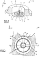
- Figs. 1 to 3 illustrate the structure of a pressure sensor according to an embodiment of the invention.
- Fig. 1 is a perspective view illustrating a pressure sensor 100 according to the embodiment
- Fig. 2 illustrates the planar structure of the pressure sensor 100 seen from the Z direction in Fig. 1
- Fig. 3 illustrates the cross-sectional structure of the pressure sensor 100 taken along line A-A in Fig. 2 . It should be noted that a cross-sectional structure at 180 degrees is illustrated only for a housing 4 in Fig. 1 .
- the pressure sensor 100 illustrated in Figs. 1 to 3 is an apparatus that detects a pressure of a measurement target fluid by transmitting, to a semiconductor chip in which a strain gauge is formed, the displacement of a diaphragm when the diaphragm is bent by the pressure of the fluid.
- the pressure sensor 100 includes two semiconductor chips 1a and 1b, supporting members 2a, 2b, 2c, and 2d, a diaphragm 3, seats 5 and 6, and the housing 4.
- the pressure sensor 100 may further include a displaying portion (for example, a liquid crystal display) or the like for indicating various types of information such as a detected pressure value to a user.
- FIGs. 1 to 3 illustrate a mechanism for transmitting the bending of the diaphragm 3 in the pressure sensor 100 to the semiconductor chips 1a and 1b, they do not illustrate other functional portions such as a circuit for processing signals output from the semiconductor chips 1a and 1b.
- the directions that are orthogonal to each other and parallel to the planar direction of the diaphragm 3 may be referred to as the X axis direction and the Y axis direction and the direction orthogonal to the planar direction (X axis and Y axis) of the diaphragm 3 may be referred to as the Z axis direction.
- the semiconductor chips 1a and 1b, the diaphragm 3, the seats 5 and 6, and the supporting members 2a to 2d are accommodated in the housing 4 made of a metal material having high corrosive resistance.
- the housing 4 is formed in a cylinder as illustrated in Figs. 1 to 3 and one end portion 4A thereof is shaped like a joint to be connected to a pipe through which the measurement target fluid flows.
- the housing 4 is filled with, for example, air and the pressure close to an inner wall 4B is, for example, the atmospheric pressure.
- the diaphragm 3 is a film that receives the pressure of the measurement target fluid and supports the semiconductor chips 1a and 1b and a supporting member 2.
- the diaphragm 3 is made of a material having high corrosive resistance such as, for example, stainless steel (SUS), ceramic, or titanium and is formed in, for example, a circle in plan view.
- the diaphragm 3 is fixed to the part of the housing 4 close to the end portion 4A and blocks the opening part of the end portion 4A of the housing 4.
- the outer peripheral edge of the diaphragm 3 is coupled to the part of the inner wall 4B of the housing 4 close to the end portion 4A without clearance.
- One surface of the diaphragm 3 acts as a pressure receiving surface (wetted surface) 3A in contact with the measurement target fluid and the other surface acts as a supporting surface 3B for supporting the semiconductor chips 1a and 1b via the supporting members 2a to 2d.
- the diaphragm 3 is bent according to the pressure difference between the pressure applied from the measurement target fluid to the pressure receiving surface 3A and the pressure (for example, the atmospheric pressure) applied to the supporting surface 3B.
- diaphragm 3 and the housing 4 of the pressure sensor may not be illustrated in the drawings of the application.
- the semiconductor chip 1a is formed in a rectangle in plan view and includes a circuit board made of a semiconductor material such as Si and the strain gauge that has resistors R1 and R2 formed in the circuit board by a known semiconductor manufacturing technique and detects a strain generated in the semiconductor chip 1a as changes in resistance values of the resistors R1 and R2.
- the semiconductor chip 1b is formed in a rectangle in plan view and includes a circuit board made of a semiconductor material such as Si and the strain gauge that has resistors R3 and R4 formed in the circuit board by a known semiconductor manufacturing technique and detects a strain generated in the semiconductor chip 1b as changes in resistance values of the resistors R3 and R4.
- one surface on which the resistors R1 and R2 included in the strain gauge are formed may be referred to below as a "principal surface 1aA” and the surface opposite to the principal surface 1aA may be referred to below as a “back surface 1aB”.
- one surface on which the resistors R3 and R4 included in the strain gauge are formed may be referred to below as a "principal surface 1bA” and the surface opposite to the principal surface 1bA may be referred to below as a "back surface 1bB".
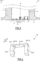
- Fig. 4 is a perspective view illustrating the semiconductor chip 1a seen from the back surface.
- a thin-walled portion (countersink) 1aC which is thinner than the part to which the supporting members 2a and 2b are coupled, is formed in the surface of the semiconductor chip 1a facing the diaphragm 3 (that is, the back surface 1aB of the semiconductor chip 1a).
- a thin-walled portion 1bC which is thinner than the part to which the supporting members 2c and 2d are coupled, is formed in the back surface 1bB of the semiconductor chip 1b similarly.
- the thin-walled portion 1aC can be formed by selectively cutting down the semiconductor chip 1a from the back surface 1aB using, for example, a known etching technique. This is true for the thin-walled portion 1bC.
- the semiconductor chip 1a and the semiconductor chip 1b are formed in the same shape so that the same stress is generated when the same force is applied.
- the semiconductor chip 1a and the semiconductor chip 1b are assumed to be formed in rectangles having the same thickness (length in the Z axis direction) and the same length and width (length in the X axis direction and length in the Y axis direction) in plan view.
- the seat 5 is a member (base) for supporting the supporting members 2a and 2c on the supporting surface 3B of the diaphragm 3.
- the seat 6 is a member (base) for supporting the supporting members 2b and 2d on the supporting surface 3B of the diaphragm 3.
- the seats 5 and 6 are formed integrally with the diaphragm 3.
- the seats 5 and 6 are made of the same material as in the diaphragm 3 and are integrally formed with the diaphragm 3 in the embodiment, as long as the seats 5 and 6 are fixed on the supporting surface 3B of the diaphragm 3, the material of the seats 5 and 6 may be different from that of the diaphragm 3 or the seats 5 and 6 may be formed separately from the diaphragm 3 and may be bonded to the supporting surface 3B using an adhesive.
- the seat 5 is disposed concentrically with the diaphragm 3 so as to make the amount of displacement of the supporting member 2a identical to the amount of displacement of the supporting member 2c supported by the seat 5 when the diaphragm 3 is bent and the seat 5 projects orthogonally from the supporting surface 3B.
- the seat 6 is disposed concentrically with the diaphragm 3 so as to make the amount of displacement of the supporting member 2b identical to the amount of displacement of the supporting member 2d supported by the seat 5 when the diaphragm 3 is bent and the seat 6 projects orthogonally from the supporting surface 3B.
- the seat 5 is formed in a ring about a center 30 of the diaphragm 3.
- the seat 6 is formed in a ring having a diameter larger than in the seat 5 about the center 30 of the diaphragm 3.
- the seats 5 and 6 are fixed to the supporting surface 3B with the axes thereof orthogonal to the supporting surface 3B.
- the supporting members 2a and 2b are structural bodies functioning as columns supporting the semiconductor chip 1a on the diaphragm 3.
- the supporting members 2c and 2d are structural bodies functioning as columns supporting the semiconductor chip 1b on the diaphragm 3.
- the supporting members 2a to 2d are formed in, for example, rectangular columns (for example, quadratic columns).
- the supporting members 2a to 2d are made of an electrically insulated material. More preferably, the supporting members 2a to 2d are made of a material that is electrically insulated, has certain rigidity, and has smaller thermal conductivity. Glass (for example, borosilicate glass (Pyrex (registered trademark))) can be illustrated as a material of the supporting members 2a to 2d.
- the supporting member 2a as a first structural body is provided orthogonally to the diaphragm 3 so that one end thereof is coupled onto the part of the seat 5 in one straight line 21 of two straight lines 21 and 22, orthogonal to each other, that pass through the center 30 of the supporting surface 3B of the diaphragm 3 in plan view and the other end thereof is coupled to the back surface 1aB of the semiconductor chip 1a.
- the supporting member 2b as a second structural body is provided orthogonally to the diaphragm 3 so that one end thereof is coupled to the part of the seat 6 in the straight line 21 in plan view and the other end is coupled to the back surface 1aB of the semiconductor chip 1a.
- the one ends thereof are coupled onto the seats 5 and 6 and the other ends thereof are coupled onto the back surfaces of the semiconductor chip 1a.
- the supporting members 2c and 2d one ends thereof are coupled onto the seats 5 and 6 and the other ends thereof are coupled onto the back surface of the semiconductor chip 1b.
- the coupling between the supporting members 2a to 2d and the semiconductor chips 1a and 1b and the coupling between the supporting members 2a to 2d and the seats 5 and 6 are performed via, for example, an adhesive.
- the one end thereof is coupled onto the seat 5 in the other straight line 22 of the above two straight lines 21 and 22 and the other end thereof is coupled to the back surface 1bB of the semiconductor chip 1b.
- the one end thereof is coupled onto the seat 6 in the straight line 22 and the other end thereof is coupled onto the back surface 1bB of the semiconductor chip 1b.
- the heights (lengths in the Z axis direction) of the supporting members 2a to 2d provided orthogonally to the diaphragm 3 are identical to each other.
- the principal surfaces 1aA and 1bA of the semiconductor chips 1a and 1b supported by the supporting members 2a to 2d are parallel to the supporting surface 3B of the diaphragm 3.
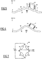
- Fig. 5 schematically illustrates the displacement of the supporting members 2a and 2b and the displacement of the semiconductor chip 1a when the diaphragm 3 is deformed in the pressure sensor 100
- Fig. 6 schematically illustrates, as a comparative example for the pressure sensor 100 according to embodiment 1, the displacement of the semiconductor chip 1a when the supporting members 2a and 2b are directly coupled to the diaphragm 3 without providing the annular seats 5 and 6.
- the supporting members 2a and 2b are directly coupled to the supporting surface 3B of the diaphragm 3 without providing the annular seats 5 and 6, if the diaphragm 3 is deformed by pressure P from the fluid, the supporting members 2a and 2b are inclined while keeping the state in which the supporting members 2a and 2b are orthogonal to the diaphragm 3. That is, the supporting member 2a and the supporting member 2b displaced in the X axis direction in addition to the Z axis direction according to the deformation of the diaphragm 3. Accordingly, the displacement of the diaphragm 3 is not appropriately transmitted to the semiconductor chip 1a and a strain is hardly generated in the semiconductor chip 1a, it is difficult to detect the pressure of the fluid using the semiconductor chip 1a.
- the widths (distances in the radial direction (X axis direction and Y axis direction) of the rings) of the coupling surfaces between the seats 5 and 6 and the diaphragm 3 are increased, the deformation of the diaphragm 3 is suppressed and the sensor sensitivity is reduced.
- the rigidity of the coupling parts between the seats 5 and 6 and the diaphragm 3 is reduced, the seats 5 and 6 are easily inclined in the X axis direction when the diaphragm 3 is deformed, and the adhesion strength with the supporting members 2a and 2b is reduced. Accordingly, the above widths need to be changed as appropriate in consideration of the requested sensor sensitivity or adhesive strength.
- the strain gauge of the pressure sensor 100 includes, for example, a bridge circuit 16 in which the two resistors (for example diffusion resistors) R1 and R2 formed on the semiconductor chip 1a are electrically connected to the resistors R3 and R4 formed on the semiconductor chip 1b. It should be noted that signal lines for connecting the resistors R1 to R4 are not illustrated in Figs. 1 to 4 .
- the semiconductor chip 1a and the semiconductor chip 1b are cut out from the semiconductor substrate of the same lot to reduce relative variations in the resistors R1 to R4.
- the pressure sensor 100 can measure the pressure of the measurement target fluid by detecting changes in the resistance values of the resistors R1 to R4 as changes in voltages caused by the stresses generated in the semiconductor chips 1a and 1b in the state in which a constant current flows through the bridge circuit 16.
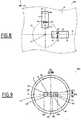
- Fig. 8 illustrates an example of disposing the resistors R1 to R4 on the semiconductor chips 1a and 1b in the pressure sensor according to embodiment 1. It should be noted that the seats 5 and 6 are not illustrated in Fig. 8 .
- the resistors R1 and R2 are formed in the region (that is, the region on the principal surface 1aA of the semiconductor chip 1a in which a tensile stress is generated) in which a stress generated in the semiconductor chip 1a is positive (+) when the diaphragm 3 is bent by the pressure of the fluid. Specifically, as illustrated in Fig. 8 , the resistors R1 and R2 are formed in the region on the principal surface 1aA corresponding to the thin-walled portion 1aC between the coupling surface of the supporting member 2a and the coupling surface of the supporting member 2b disposed in the straight line 21 in plan view in the semiconductor chip 1a.
- the resistors R3 and R4 are formed in the region (that is, the region on the principal surface 1bA of the semiconductor chip 1b in which a tensile stress is generated) in which a stress generated in the semiconductor chip 1b is positive (+) when the diaphragm 3 is bent by the pressure of the fluid. Specifically, as illustrated in Fig. 8 , the resistors R3 and R4 are formed in the region on the principal surface 1bA corresponding to the thin-walled portion 1bC between the coupling surface of the supporting member 2c and the coupling surface of the supporting member 2d disposed in the straight line 22 in plan view in the semiconductor chip 1b.
- the resistors R1 to R4 are formed in, for example, rectangles in plan view. Although the resistors R1 to R4 are formed in the same rectangles (strips) in plan view and have the same resistance value in the embodiment, the invention is not limited to this embodiment.
- the resistor R1 and the resistor R2 may extend in directions different from each other in plan view and the resistor R3 and the resistor R4 may extend in directions different from each other in plan view.
- the direction in which the resistors R1 to R4 extend refers to the direction in which a current flows when a voltage is applied to the resistors R1 to R4.
- the resistor R1 and the resistor R4 may extend in the same direction in plan view and the resistor R2 and the resistor R3 may extend in the same direction in plan view.
- the direction in which the resistor R1 and the resistor R4 extend may be orthogonal to the direction in which the resistor R2 and the resistor R3 extend.
- the resistor R1 and the resistor R4 may extend in a direction parallel to the straight line 21 and the resistor R2 and the resistor R3 may extend in a direction parallel to the straight line 22.
- the resistors R1 to R4 may be disposed equidistantly (with a deviation ranging within, for example, plus or minus 10 percent) from the center 30 of the diaphragm 3.
- the distances from the center 30 of the diaphragm 3 to the centers of the rectangular resistors R1, R2, R3, and R4 may be the same.
- the resistor R1, R2, R3, and R4 may be disposed in the circumference of a circle 15 having the same center 30 as the diaphragm 3 in plan view.
- the diameter of the circle 15 is not particularly limited as long as the circle 15 fits within the thin-walled portions 1aC and 1bC of the semiconductor chips 1a and 1b.
- the pressure sensor 100 configured as described above has the following effects. The effects of the pressure sensor 100 will be described below by comparing the pressure sensor 100 according to embodiment 1 with a different pressure sensor 901.
- the pressure sensor 901 which is the comparative example of the pressure sensor 100 according to embodiment 1, will be described.
- Fig. 9 illustrates the pressure sensor 901 as a comparative example.
- the pressure sensor 901 has a semiconductor chip 1X that is rectangular in plan view and three supporting members 2ax, 2bx, and 2cx for supporting the semiconductor chip 1X provided side by side orthogonally in a straight line 25 passing through the center 30 of the supporting surface 3B of the diaphragm 3.
- Fig. 10 illustrates the result of simulation of a sensor output (an output signal of the bridge circuit) of the above pressure sensor 901 using the finite element (FEM) method.
- the horizontal axis represents the distance in the longitudinal direction of the semiconductor chip 1X from the center in the longitudinal direction of the semiconductor chip 1X when the center is assumed to be 0 and the vertical axis represents the magnitude of the output signal (
- reference numeral P1 represents the magnitude of the output signal of the bridge circuit 16 obtained by conversion based on the stress distribution of the resistors R1 to R4 when changing the positions in which the resistors R1 to R4 are formed with respect to the center of the semiconductor chip 1X when a screw 52 of a clamp 50 is fixed at position P1 in the straight line 25 illustrated in Fig. 9
- reference numeral P2 represents the magnitude of the output signal of the bridge circuit 16 obtained by conversion based on the stress distribution of the resistors R1 to R4 when changing the positions in which the resistors R1 to R4 are formed with respect to the center of the semiconductor chip 1X when the screw 52 of the clamp 50 is fixed at position P2 in the straight line 26 illustrated in Fig. 9 .
- the shift amount of the zero point of a sensor output (an output signal of the bridge circuit 16 included in the strain gauge) becomes smaller than in the pressure sensor 901 as described later.
- the pressure sensor 100 according to embodiment 1 will be described in detail below.
- Fig. 11 illustrates the fixation position of the screw of the clamp for connecting a pipe to the pressure sensor 100 according to embodiment 1.
- Fig. 12A is a contour diagram (isoline diagram) illustrating the displacement in the Z axis direction of the diaphragm 3 when the screw 52 of the clamp 50 is fixed at position P1 in the straight line 22 illustrated in Fig. 11
- Fig. 12B is a contour diagram illustrating the displacement in the Z axis direction of the semiconductor chips 1a and 1b when the screw 52 of the clamp 50 is fixed at position P1 the straight line 22 illustrated in Fig. 11 .
- Fig. 13A is a contour diagram (isoline diagram) illustrating the displacement in the Z axis direction of the diaphragm 3 when the screw 52 of the clamp 50 is fixed at position P2 in the straight line 21 illustrated in Fig. 11
- Fig. 13B is a contour diagram illustrating the displacement in the Z axis direction of the semiconductor chips 1a and 1b when the screw 52 of the clamp 50 is fixed at position P2 in the straight line 21 illustrated in Fig. 11 .
- the four supporting members 2a to 2d are fixed in the two straight lines 21 and 22, orthogonal to each other, that pass through the center 30 of the diaphragm 3 in plan view and the supporting members 2a to 2d support the semiconductor chips 1a and 1b that are rectangular in plan view using the supporting surface 3B of the diaphragm 3 in the pressure sensor 100 according to the embodiment, the displacements in the Z axis direction of the semiconductor chips 1a and 1b are also reversed as illustrated in Figs. 12B and 13B .
- the resistors R1 to R4 included in the strain gauge are disposed in the regions of the semiconductor chips 1a and 1b in which stress distributions in directions opposite to each other are generated when the clamp 50 is tightened by the screw 52.
- a pair of resistors (resistors R1 and R2) is formed in the region between the supporting member 2a and the supporting member 2b in the semiconductor chip 1a and another pair of resistors (resistors R3 and R4) is formed in the region between the supporting member 2c and the supporting member 2d in the semiconductor chip 1b.
- the directions in which the resistors R1 to R4 extend only need to be determined so that the resistance value of the resistor R1 and the resistance value of the resistor R4 change in the same direction and the resistance value of the resistor R2 and the resistance value of the resistor R3 change in the same direction when the screw 52 of the clamp 50 is tightened.
- the resistor R1 and the resistor R4 extend in the same direction and the resistor R2 and the resistor R3 extend in the same direction.
- the deviation of the resistance ratio between the resistor R2 and the resistor R3 close to an output signal Vb of the bridge circuit 16 included in the strain gauge can be suppressed.
- Fig. 14 illustrates the result of simulation of an output signal of the bridge circuit 16 of the pressure sensor 100 using the FEM when the position of the screw 52 for fixing the clamp 50 is changed as illustrated in Fig. 11 .
- Fig. 14 illustrates the result of simulation when the resistors R1 to R4 of the bridge circuit 16 of the pressure sensor 100 are disposed as illustrated in Fig. 8 .
- the horizontal axis represents the distance in the longitudinal direction of the semiconductor chips 1a and 1b from the centers in the longitudinal direction of the semiconductor chips 1a and 1b when the centers are assumed to be 0 and the vertical axis represents the magnitude of the output signal (IVa - Vbl) of the bridge circuit 16 obtained by conversion based on the stress distribution of the four resistors R1 to R4 of the semiconductor chips 1a and 1b.
- This simulation assumes that the semiconductor chip 1a and the semiconductor chip 1b have the same shape and the positions of the resistor R1 and the resistor R4 on the semiconductor chip 1a are the same (disposed in the circumference of the circle 15 in Fig. 8 ) as the positions of the resistor R2 and the resistor R3 on the semiconductor chip 1b.
- reference numeral P1 represents the magnitude of the output signal of the bridge circuit 16 obtained by conversion based on the stress distribution of the resistors R1 to R4 when changing the positions in which the resistors R1 to R4 are formed with respect to the centers of the semiconductor chips 1a and 1b when the screw 52 of the clamp 50 is fixed at position P1 in the straight line 22 illustrated in Fig. 11
- reference numeral P2 represents the magnitude of the output signal of the bridge circuit 16 obtained by conversion based on the stress distribution of the resistors R1 to R4 when changing the positions in which the resistors R1 to R4 are formed with respect to the centers of the semiconductor chips 1a and 1b when the screw 52 of the clamp 50 is fixed at position P2 in the straight line 21 illustrated in Fig. 11 .
- Va - Vbl of the bridge circuit 16) of the pressure sensor 100 when the screw 52 of the clamp 50 is tightened is suppressed and variations in the above shift amount caused by the differences in the tightening position of the screw 52 of the clamp 50 can be also suppressed.
- the resistors R1 and R2 are disposed in the region between the two supporting members 2a and 2b for supporting the semiconductor chip 1a and the resistors R3 and R4 are disposed in the region between the two supporting members 2c and 2d for supporting the semiconductor chip 1b in the semiconductor chips 1a and 1b disposed in the two straight lines 21 and 22, orthogonal to each other, that pass through the center 30 of the diaphragm 3, fluctuations in the resistance ratio between the resistor R1 and the resistor R4 and fluctuations in the resistance ratio between the resistor R2 and the resistor R3 when the screw 52 of the clamp 50 is tightened can be suppressed.
- the resistance values of the resistor R1 and the resistor R4 can be changed by substantially the same amount in the same direction and the resistance values of the resistor R2 and the resistor R3 can be changed by substantially the same amount in the same direction when the screw 52 of the clamp 50 is tightened. Accordingly, the shift amount of the zero point of a sensor output (output signal
- the resistors R1 to R4 are formed in positions (for example, in the circumference of the circle 15) equidistant from the center 30 of the diaphragm 3 in plan view, it is possible to equalize the change amounts of the resistance values of the resistors R1 to R4 caused by stresses in the semiconductor chips 1a and 1b generated when the screw 52 is tightened, enabling further reduction in the shift amount of the zero point of a sensor output and variations in the shift amount.
- the deviation amount of the resistance ratio between the resistor R1 and the resistor R4 close to the output signal Va of the bridge circuit 16 and the deviation amount of the resistance ratio between the resistor R2 and the resistor R3 close to the output signal Vb of the bridge circuit 16 can be further increased when a pressure is applied to the pressure receiving surface 3A of the diaphragm 3 by the pressure from the measurement target fluid by making the direction in which the resistor R1 and the resistor R4 extend subststantially orthogonal to the direction in which the resistor R2 and the resistor R3 extend, the sensor sensitivity of the pressure sensor 100 with respect to the pressure applied to the pressure receiving surface 3A of the diaphragm 3 can be further improved.
- the sensor sensitivity of the pressure sensor 100 with respect to the pressure applied to the pressure receiving surface 3A of the diaphragm 3 can be further improved.
- the resistors R1 and the resistor R2 are disposed side by side in a direction (direction parallel to the straight line 22) parallel to a shorter side of the semiconductor chip 1a and the resistor R3 and the resistor R4 are disposed side by side in a direction (direction parallel to the straight line 21) parallel to a shorter side of the semiconductor chip 1b in the embodiment described above (see Fig. 8 ), the resistors R1 to R4 only need to be disposed so that the resistance value of the resistor R1 and the resistance value of the resistor R4 are changed in the same direction and the resistance value of the resistor R2 and the resistance value of the resistor R3 are changed in the same direction when the screw 52 of the clamp 50 is tightened.
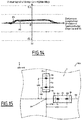
- the resistors R1 to R4 may be disposed as illustrated in Fig. 15 .
- Fig. 15 illustrates another example of disposing the resistors of the pressure sensor according to embodiment 1.
- the resistor R1 and the resistor R2 are disposed side by side in a direction (direction parallel to the straight line 21) parallel to a longer side of the semiconductor chip 1a and the resistor R3 and resistor R4 are disposed side by side in a direction (direction parallel to the straight line 22) parallel to a longer side of the semiconductor chip 1b.
- the resistors R1 to R4 are formed in, for example, rectangles in plan view and extend in the same direction.
- the resistors R1 to R4 extend in a direction parallel to the straight line 22.
- a distance (for example, the distance to the center of the resistor R1) LR1 from the center 30 of the diaphragm 3 to the resistor R1 may be equal to (with a error of, for example, plus or minus 10 percent) a distance (for example, the distance to the center of the resistor R4) LR4 from the center 30 of the diaphragm 3 to the resistor R4, and a distance (for example, the distance to the center of the resistor R2) LR2 from the center 30 of the diaphragm 3 to the resistor R2 may be equal to (with a error of, for example, plus or minus 10 percent) a distance (for example, the distance to the center of the resistor R3) LR3 from the center 30 of the diaphragm 3 to the resistor R3.
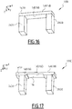
- the thin-walled portion 1aC is formed on the back surface 1aB of the semiconductor chip 1a in the above embodiment, as long as sufficient sensor sensitivity can be obtained as the pressure sensor, the thickness between the principal surface 1aA and the back surface 1aB may be uniform without forming the thin-walled portion 1aC on the semiconductor chip 1a as in a pressure sensor 100B illustrated in Fig. 16 . This is true for the semiconductor chip 1b.
- the supporting members 2a and 2b are coupled to the back surface 1aB of the semiconductor chip 1a so that the side surfaces of the supporting members 2a and 2b are flush with the side surfaces of the semiconductor chip 1a in the above embodiment
- the supporting members 2a, 2b, 2c, and 2d may be coupled to positions inward of the side surfaces of the semiconductor chips 1a and 1b.
- the supporting members 2a and 2b may be coupled to positions closer to a center 10 of the semiconductor chip 1a than in the pressure sensor 100 in Fig. 4 .
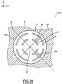
- the seats 5 and 6 are formed continuously along the circumferential direction thereof in the above embodiment, the invention is not limited to the embodiment and the seats 5 and 6 may be formed intermittently along the circumferences thereof.
- the seats 5 and 6 may be quartered so that the seats 5 and 6 have four intermittent parts in the circumferential direction.
- the diameter of the circle 15 is not limited to that illustrated in Fig. 8 or the like and it will be appreciated that the diameter may be changed depending on the requested performance or the like.
- Fig. 15 illustrates the case in which the resistors R1 to R4 extend in a direction parallel to the straight line 22 as an example of the case in which the resistors R1 to R4 extend in the same direction
- the invention is not limited to this example and the resistors R1 to R4 may extend in a direction parallel to the straight line 21.
- resistors R1 to R4 are rectangular in plan view in the embodiment described above, the invention is not limited to the embodiment. For example, they may be square in plan view.
Landscapes
- Physics & Mathematics (AREA)
- General Physics & Mathematics (AREA)
- Measuring Fluid Pressure (AREA)
- Pressure Sensors (AREA)
Abstract
Description
- The present invention relates to a pressure sensor and, for example, to a sanitary pressure sensor.
- Generally, it is necessary to meet strict conditions such as corrosive resistance, cleanness, reliability, and versatility, for a pressure sensor for detecting the pressure of a fluid to be permitted as a sanitary pressure sensor that needs consideration to sanitation used in production sites for food, drugs, and the like.
- For example, to ensure corrosive resistance, a sanitary pressure sensor needs to include a material having high corrosive resistance, such as stainless steel (SUS), ceramic, or titanium in the wetted part in contact with a measurement target fluid (for example, liquid) for the pressure. In addition, to ensure cleanness, a sanitary pressure sensor needs to have a flash diaphragm structure that enables easy cleaning and high heat and impact resistance against steam cleaning. In addition, to ensure reliability, a sanitary pressure sensor needs to have a structure (oil free structure) that does not include encapsulant and a structure (barrier high rigidity) that makes it difficult to break a diaphragm.
- Since materials and structures that can be used for a sanitary pressure sensor are restricted as compared with other pressure sensors as described above, it is difficult to improve the sensitivity. For example, to achieve a structure that makes it difficult to break a diaphragm, although the film thickness of the diaphragm needs to be increased (the aspect ratio of the diameter to the thickness of the diaphragm needs to be reduced), increase in the thickness of a diaphragm generally reduces the sensor sensitivity because the amount of deformation of a diaphragm becomes minute. Accordingly, a technique for accurately detecting minute deformation of a diaphragm is necessary for a sanitary pressure sensor.
- For example,
JP 2004-45140 A JP S63-217671 A - Specifically, in the conventional load conversion type pressure sensor disclosed in
JP 2004-45140 A JP S63-217671 A JP S63-217671 A - Generally, a sanitary pressure sensor has a joint (for example, a ferrule joint) in a connection part with a pipe through which a measurement target fluid flows.
- Connection between the pipe and the sanitary pressure sensor is made using a connection member called a clamp band (also referred to below as a "clamp" simply) as illustrated in
Fig. 19 . Specifically, as illustrated inFig. 20 , the joint for apipe 200 and the joint for asanitary pressure sensor 300 are disposed so as to face each other, the two joints are clamped bysemicircular fixing portions 51A and 51B of a clamp 50, and thefixing portions 51A and 51B are tightened by ascrew 52, thereby making connection between thepipe 200 and thesanitary pressure sensor 300. - However, when connection between the pipe and the sanitary pressure sensor is made by the clamp, the diaphragm of the sanitary pressure sensor is deformed to no small extent, possibly shifting the zero point (offset) of a sensor output. In the case of the pressure sensor having a semiconductor chip that is rectangular in plan view as disclosed
JP 2004-45140 A JP S63-217671 A - The invention addresses the above problems with an object of suppressing variations in the shift amount of the zero point of a sensor output when a pipe through which a measurement target fluid is connected to a pressure sensor via a clamp.
- A pressure sensor (100) according to the invention includes a diaphragm (3) having a first principal surface (3A) receiving a pressure of a measurement target fluid and a second principal surface (3B) opposite to the first principal surface, a first seat (5) provided in a deformed area of the second principal surface in which the diaphragm is deformed when a pressure higher than a pressure applied in the second principal surface is applied in the first principal surface, the first seat being disposed concentrically with the diaphragm in plan view and projecting from the second principal surface orthogonally, a second seat (6) provided in the deformed area concentrically with the diaphragm in plan view and projecting from the second principal surface orthogonally, the second seat having a diameter larger than in the first seat, a first semiconductor chip (1a) having a first resistor (R1) and a second resistor (R2) on one surface thereof, the first resistor and the second resistor being included in a strain gauge, a second semiconductor chip (1b) having a third resistor (R3) and a fourth resistor (R4) on one surface thereof, the third resistor and the fourth resistor being included in the strain gauge, a first structural body (2a) provided orthogonally so that one end thereof is coupled to a part of the first seat, the part being disposed in a first straight line (21) passing through the center of the second principal surface of the diaphragm in plan view, and the other end thereof is coupled to the other surface of the first semiconductor chip, a second structural body (2b) provided orthogonally so that one end thereof is coupled to a part of the second seat, the part being disposed in the first straight line in plan view, and the other end thereof is coupled to the other surface of the first semiconductor chip, a third structural body (2c) provided orthogonally so that one end thereof is coupled to a part of the first seat, the part being disposed in a second straight line (22) passing through the center of the second principal surface and orthogonal to the first straight line in plan view and the other end thereof is coupled to the other surface of the second semiconductor chip, and a fourth structural body (2d) provided orthogonally so that one end thereof is coupled to a part of the second seat, the part being disposed in the second straight line in plan view, and the other end thereof is coupled to the other surface of the second semiconductor chip, in which the first resistor and the second resistor are formed in a region between a coupling surface to which the first structural body is coupled and a coupling surface to which the second structural body is coupled in plan view in the first semiconductor chip and the third resistor and the fourth resistor are formed in a region between a coupling surface to which the third structural body is coupled and a coupling surface to which the fourth structural body is coupled in plan view in the second semiconductor chip.
- In the pressure sensor described above, preferably, the first semiconductor chip is formed in a rectangle and the first semiconductor chip is disposed so that a longer side thereof is parallel to the first straight line, the second semiconductor chip is formed in a rectangle and the second semiconductor chip is disposed so that a longer side thereof is parallel to the second straight line, the first resistor and the second resistor are disposed side by side in a direction parallel to a shorter side of the first semiconductor chip and extend in directions different from each other, the third resistor and the fourth resistor are disposed side by side in a direction parallel to a shorter side of the second semiconductor chip and extend in directions different from each other.
- In the pressure sensor described above, preferably, the first resistor and the fourth resistor extend in the same direction and the second resistor and the third resistor extend in a direction orthogonal to the direction in which the first resistor and the fourth resistor extend.
- In the pressure sensor described above, preferably, the first resistor, the second resistor, the third resistor, and the fourth resistor are disposed equidistantly from the center of the second principal surface of the diaphragm.
- In the pressure sensor described above, preferably, the first semiconductor chip is formed in a rectangle and the first semiconductor chip is disposed so that a longer side thereof is parallel to the first straight line, the second semiconductor chip is formed in a rectangle and the second semiconductor chip is disposed so that a longer side thereof is parallel to the second straight line, the first resistor and the second resistor are disposed side by side in a direction parallel to the longer side of the first semiconductor chip, and the third resistor and the fourth resistor are disposed side by side in a direction parallel to the longer side of the second semiconductor chip.
- In the pressure sensor described above, preferably, the first resistor, the second resistor, the third resistor, and the fourth resistor extend in the same direction.
- In the pressure sensor described above, preferably, the first resistor and the fourth resistor are disposed equidistantly from the center of the second principal surface of the diaphragm and the second resistor and the third resistor are disposed equidistantly from the center of the second principal surface of the diaphragm.
- In the pressure sensor described above, preferably, the first semiconductor chip has a first thin-walled portion (1aC) thinner than regions to which the first structural body and the second structural body are coupled, the second semiconductor chip has a second thin-walled portion (1bC) thinner than regions to which the third structural body and the fourth structural body are coupled, the first resistor and the second resistor are formed in a region on the one surface of the first semiconductor chip, the region corresponding to the first thin-walled portion, and the third resistor and the fourth resistor are formed in a region on the one surface of the second semiconductor chip, the region corresponding to the second thin-walled portion.
- It should be noted that reference numerals in the drawings corresponding to components of the invention are enclosed in parentheses in the above description.
- As described above, according to the invention, it is possible to suppress variations in the shift amount of the zero point of a sensor output when a pipe through which the measurement target fluid flows is connected to a pressure sensor connected via a clamp.
-
- [
Fig. 1] Fig. 1 is a perspective view illustrating the structure of a pressure sensor according to an embodiment of the invention. - [
Fig. 2] Fig. 2 is a plan view illustrating the structure of the pressure sensor according to the embodiment of the invention. - [
Fig. 3] Fig. 3 is a cross-sectional view illustrating the structure of the pressure sensor according to the embodiment of the invention. - [
Fig. 4] Fig. 4 is a perspective view illustrating asemiconductor chip 1a seen from the back surface. - [
Fig. 5] Fig. 5 schematically illustrates the displacement of supportingmembers semiconductor chip 1a when adiaphragm 3 is deformed in the pressure sensor according to the embodiment of the invention. - [
Fig. 6] Fig. 6 schematically illustrates the displacement of thesemiconductor chip 1a when the supportingmembers diaphragm 3 without providingannular seats - [
Fig. 7] Fig. 7 illustrates the structure of a bridge circuit as a strain gauge. - [
Fig. 8] Fig. 8 illustrates an example of disposing resistors constituting the strain gauge on the semiconductor chips. - [
Fig. 9] Fig. 9 illustrates apressure sensor 901 in which asemiconductor chip 1X that is rectangular in plan view is supported by supporting members 2ax, 2bx, and 2cx at a position close to acenter 30 of a supportingsurface 3B of thediaphragm 3 as a comparative example of the pressure sensor according to the embodiment of the invention. - [
Fig. 10] Fig. 10 illustrates the result of simulation of a sensor output from thepressure sensor 901 inFig. 9 using the finite element method. - [
Fig. 11] Fig. 11 illustrates the fixation position of a screw of a clamp for connecting a pipe to the pressure sensor according to the embodiment of the invention. - [
Fig. 12A] Fig. 12A is a contour diagram illustrating the displacement in the Z axis direction of thediaphragm 3 when ascrew 52 of a clamp 50 is fixed at position P1 illustrated inFig. 11 . - [
Fig. 12B] Fig. 12B is a contour diagram illustrating the displacement in the Z axis direction of thesemiconductor chip 1 when thescrew 52 of the clamp 50 is fixed at position P1 illustrated inFig. 11 . - [
Fig. 13A] Fig. 13A is a contour diagram illustrating the displacement in the Z axis direction of thediaphragm 3 when thescrew 52 of the clamp 50 is fixed at position P2 illustrated inFig. 11 . - [
Fig. 13B] Fig. 13B is a contour diagram illustrating the displacement in the Z axis direction of thesemiconductor chip 1 when thescrew 52 of the clamp 50 is fixed at position P2 illustrated inFig. 11 . - [
Fig. 14] Fig. 14 illustrates the result of simulation of a sensor output from the pressure sensor according to the embodiment of the invention. - [
Fig. 15] Fig. 15 illustrates another example of the disposition of resistors in the pressure sensor according to the embodiment of the invention. - [
Fig. 16] Fig. 16 is a perspective view illustrating a semiconductor chip of a pressure sensor according to another embodiment of the invention seen from the back surface. - [
Fig. 17] Fig. 17 is a perspective view illustrating a semiconductor chip of a pressure sensor according to another embodiment seen from the back surface. - [
Fig. 18] Fig. 18 illustrates an example of a seat having slits in the circumferential direction. - [
Fig. 19] Fig. 19 illustrates the planar structure of a clamp for connecting the pressure sensor to the pipe. - [
Fig. 20] Fig. 20 illustrates a connection structure for the pressure sensor and the pipe via the clamp. - Embodiments of the present invention will be described below with reference to the drawings. It should be noted that components common to the individual embodiments are given the same reference numerals to omit the repeated descriptions.
-
Figs. 1 to 3 illustrate the structure of a pressure sensor according to an embodiment of the invention. -
Fig. 1 is a perspective view illustrating apressure sensor 100 according to the embodiment,Fig. 2 illustrates the planar structure of thepressure sensor 100 seen from the Z direction inFig. 1 , andFig. 3 illustrates the cross-sectional structure of thepressure sensor 100 taken along line A-A inFig. 2 . It should be noted that a cross-sectional structure at 180 degrees is illustrated only for ahousing 4 inFig. 1 . - The
pressure sensor 100 illustrated inFigs. 1 to 3 is an apparatus that detects a pressure of a measurement target fluid by transmitting, to a semiconductor chip in which a strain gauge is formed, the displacement of a diaphragm when the diaphragm is bent by the pressure of the fluid. - Specifically, the
pressure sensor 100 includes twosemiconductor chips members diaphragm 3,seats housing 4. Although not illustrated, thepressure sensor 100 may further include a displaying portion (for example, a liquid crystal display) or the like for indicating various types of information such as a detected pressure value to a user. - Although
Figs. 1 to 3 illustrate a mechanism for transmitting the bending of thediaphragm 3 in thepressure sensor 100 to thesemiconductor chips semiconductor chips - In addition, the directions that are orthogonal to each other and parallel to the planar direction of the
diaphragm 3 may be referred to as the X axis direction and the Y axis direction and the direction orthogonal to the planar direction (X axis and Y axis) of thediaphragm 3 may be referred to as the Z axis direction. - The
semiconductor chips diaphragm 3, theseats members 2a to 2d are accommodated in thehousing 4 made of a metal material having high corrosive resistance. Thehousing 4 is formed in a cylinder as illustrated inFigs. 1 to 3 and oneend portion 4A thereof is shaped like a joint to be connected to a pipe through which the measurement target fluid flows. Thehousing 4 is filled with, for example, air and the pressure close to aninner wall 4B is, for example, the atmospheric pressure. - The
diaphragm 3 is a film that receives the pressure of the measurement target fluid and supports thesemiconductor chips diaphragm 3 is made of a material having high corrosive resistance such as, for example, stainless steel (SUS), ceramic, or titanium and is formed in, for example, a circle in plan view. - The
diaphragm 3 is fixed to the part of thehousing 4 close to theend portion 4A and blocks the opening part of theend portion 4A of thehousing 4. For example, the outer peripheral edge of thediaphragm 3 is coupled to the part of theinner wall 4B of thehousing 4 close to theend portion 4A without clearance. - One surface of the
diaphragm 3 acts as a pressure receiving surface (wetted surface) 3A in contact with the measurement target fluid and the other surface acts as a supportingsurface 3B for supporting thesemiconductor chips members 2a to 2d. Thediaphragm 3 is bent according to the pressure difference between the pressure applied from the measurement target fluid to thepressure receiving surface 3A and the pressure (for example, the atmospheric pressure) applied to the supportingsurface 3B. - It should be noted that the
diaphragm 3 and thehousing 4 of the pressure sensor may not be illustrated in the drawings of the application. - The
semiconductor chip 1a is formed in a rectangle in plan view and includes a circuit board made of a semiconductor material such as Si and the strain gauge that has resistors R1 and R2 formed in the circuit board by a known semiconductor manufacturing technique and detects a strain generated in thesemiconductor chip 1a as changes in resistance values of the resistors R1 and R2. - As in the
semiconductor chip 1a, thesemiconductor chip 1b is formed in a rectangle in plan view and includes a circuit board made of a semiconductor material such as Si and the strain gauge that has resistors R3 and R4 formed in the circuit board by a known semiconductor manufacturing technique and detects a strain generated in thesemiconductor chip 1b as changes in resistance values of the resistors R3 and R4. - In the
semiconductor chip 1a, one surface on which the resistors R1 and R2 included in the strain gauge are formed may be referred to below as a "principal surface 1aA" and the surface opposite to the principal surface 1aA may be referred to below as a "back surface 1aB". In thesemiconductor chip 1b, one surface on which the resistors R3 and R4 included in the strain gauge are formed may be referred to below as a "principal surface 1bA" and the surface opposite to the principal surface 1bA may be referred to below as a "back surface 1bB". -
Fig. 4 is a perspective view illustrating thesemiconductor chip 1a seen from the back surface. - As illustrated in
Fig. 4 , a thin-walled portion (countersink) 1aC, which is thinner than the part to which the supportingmembers semiconductor chip 1a facing the diaphragm 3 (that is, the back surface 1aB of thesemiconductor chip 1a). Although not illustrated, a thin-walled portion 1bC, which is thinner than the part to which the supportingmembers semiconductor chip 1b similarly. - The thin-walled portion 1aC can be formed by selectively cutting down the
semiconductor chip 1a from the back surface 1aB using, for example, a known etching technique. This is true for the thin-walled portion 1bC. - The
semiconductor chip 1a and thesemiconductor chip 1b are formed in the same shape so that the same stress is generated when the same force is applied. In the embodiment, as an example, thesemiconductor chip 1a and thesemiconductor chip 1b are assumed to be formed in rectangles having the same thickness (length in the Z axis direction) and the same length and width (length in the X axis direction and length in the Y axis direction) in plan view. - The
seat 5 is a member (base) for supporting the supportingmembers surface 3B of thediaphragm 3. In addition, theseat 6 is a member (base) for supporting the supportingmembers surface 3B of thediaphragm 3. Theseats diaphragm 3. - Although the
seats diaphragm 3 and are integrally formed with thediaphragm 3 in the embodiment, as long as theseats surface 3B of thediaphragm 3, the material of theseats diaphragm 3 or theseats diaphragm 3 and may be bonded to the supportingsurface 3B using an adhesive. - As illustrated in
Fig. 2 , theseat 5 is disposed concentrically with thediaphragm 3 so as to make the amount of displacement of the supportingmember 2a identical to the amount of displacement of the supportingmember 2c supported by theseat 5 when thediaphragm 3 is bent and theseat 5 projects orthogonally from the supportingsurface 3B. Similarly, theseat 6 is disposed concentrically with thediaphragm 3 so as to make the amount of displacement of the supportingmember 2b identical to the amount of displacement of the supportingmember 2d supported by theseat 5 when thediaphragm 3 is bent and theseat 6 projects orthogonally from the supportingsurface 3B. - More specifically, the
seat 5 is formed in a ring about acenter 30 of thediaphragm 3. In addition, theseat 6 is formed in a ring having a diameter larger than in theseat 5 about thecenter 30 of thediaphragm 3. Theseats surface 3B with the axes thereof orthogonal to the supportingsurface 3B. - The supporting
members semiconductor chip 1a on thediaphragm 3. Similarly, the supportingmembers semiconductor chip 1b on thediaphragm 3. - The supporting
members 2a to 2d are formed in, for example, rectangular columns (for example, quadratic columns). In addition, the supportingmembers 2a to 2d are made of an electrically insulated material. More preferably, the supportingmembers 2a to 2d are made of a material that is electrically insulated, has certain rigidity, and has smaller thermal conductivity. Glass (for example, borosilicate glass (Pyrex (registered trademark))) can be illustrated as a material of the supportingmembers 2a to 2d. - The supporting
member 2a as a first structural body is provided orthogonally to thediaphragm 3 so that one end thereof is coupled onto the part of theseat 5 in onestraight line 21 of twostraight lines center 30 of the supportingsurface 3B of thediaphragm 3 in plan view and the other end thereof is coupled to the back surface 1aB of thesemiconductor chip 1a. In addition, the supportingmember 2b as a second structural body is provided orthogonally to thediaphragm 3 so that one end thereof is coupled to the part of theseat 6 in thestraight line 21 in plan view and the other end is coupled to the back surface 1aB of thesemiconductor chip 1a. - As illustrated in
Figs. 1 to 3 , in the supportingmembers seats semiconductor chip 1a. In the supportingmembers seats semiconductor chip 1b. The coupling between the supportingmembers 2a to 2d and thesemiconductor chips members 2a to 2d and theseats - In the supporting
member 2c as a third structural body, the one end thereof is coupled onto theseat 5 in the otherstraight line 22 of the above twostraight lines semiconductor chip 1b. In addition, in the supportingmember 2d as a fourth structural body, the one end thereof is coupled onto theseat 6 in thestraight line 22 and the other end thereof is coupled onto the back surface 1bB of thesemiconductor chip 1b. - The heights (lengths in the Z axis direction) of the supporting
members 2a to 2d provided orthogonally to thediaphragm 3 are identical to each other. The principal surfaces 1aA and 1bA of thesemiconductor chips members 2a to 2d are parallel to the supportingsurface 3B of thediaphragm 3. - Next, the principle of how a stress is generated in the
semiconductor chips pressure sensor 100 according toembodiment 1 will be described. Since there is no difference in the principle of generation of a stress between thesemiconductor chip 1a and thesemiconductor chip 1b, the principle of generation of a stress is described only for thesemiconductor chip 1a as an example. -
Fig. 5 schematically illustrates the displacement of the supportingmembers semiconductor chip 1a when thediaphragm 3 is deformed in thepressure sensor 100, andFig. 6 schematically illustrates, as a comparative example for thepressure sensor 100 according toembodiment 1, the displacement of thesemiconductor chip 1a when the supportingmembers diaphragm 3 without providing theannular seats - First, as illustrated in
Fig. 6 , when the supportingmembers surface 3B of thediaphragm 3 without providing theannular seats diaphragm 3 is deformed by pressure P from the fluid, the supportingmembers members diaphragm 3. That is, the supportingmember 2a and the supportingmember 2b displaced in the X axis direction in addition to the Z axis direction according to the deformation of thediaphragm 3. Accordingly, the displacement of thediaphragm 3 is not appropriately transmitted to thesemiconductor chip 1a and a strain is hardly generated in thesemiconductor chip 1a, it is difficult to detect the pressure of the fluid using thesemiconductor chip 1a. - In contrast, in the
pressure sensor 100 according toembodiment 1, as illustrated inFig. 5 , when thediaphragm 3 is deformed by pressure P from the fluid, theseats seats diaphragm 3. As a result, the displacement in the Z axis direction of thediaphragm 3 that depends on the distance from the center of thediaphragm 3 is mainly transmitted to the supportingmembers - This causes a tensile stress that depends on the displacement difference in the Z axis direction between the supporting
member 2a and the supportingmember 2b in the region in thesemiconductor chip 1a close to the principal surface 1aA. Accordingly, if the resistors R1 and R2 included in the above strain gauge (bridge circuit) are formed appropriately in the region in thesemiconductor chip 1a in which the above tensile stress is generated, it is possible to detect the pressure of the measurement target fluid highly accurately. - Since the
semiconductor chip 1b is supported by two columns (supportingmembers seats diaphragm 3 as in thesemiconductor chip 1a, a stress is generated in the same principle as in thesemiconductor chip 1a. - As the widths (distances in the radial direction (X axis direction and Y axis direction) of the rings) of the coupling surfaces between the
seats diaphragm 3 are increased, the deformation of thediaphragm 3 is suppressed and the sensor sensitivity is reduced. In contrast, as the above widths are reduced, the rigidity of the coupling parts between theseats diaphragm 3 is reduced, theseats diaphragm 3 is deformed, and the adhesion strength with the supportingmembers - Next, the strain gauge of the
pressure sensor 100 will be specifically described. - As illustrated in
Fig. 7 , the strain gauge of thepressure sensor 100 includes, for example, abridge circuit 16 in which the two resistors (for example diffusion resistors) R1 and R2 formed on thesemiconductor chip 1a are electrically connected to the resistors R3 and R4 formed on thesemiconductor chip 1b. It should be noted that signal lines for connecting the resistors R1 to R4 are not illustrated inFigs. 1 to 4 . - Preferably, the
semiconductor chip 1a and thesemiconductor chip 1b are cut out from the semiconductor substrate of the same lot to reduce relative variations in the resistors R1 to R4. - The
pressure sensor 100 can measure the pressure of the measurement target fluid by detecting changes in the resistance values of the resistors R1 to R4 as changes in voltages caused by the stresses generated in thesemiconductor chips bridge circuit 16. -
Fig. 8 illustrates an example of disposing the resistors R1 to R4 on thesemiconductor chips embodiment 1. It should be noted that theseats Fig. 8 . - The resistors R1 and R2 are formed in the region (that is, the region on the principal surface 1aA of the
semiconductor chip 1a in which a tensile stress is generated) in which a stress generated in thesemiconductor chip 1a is positive (+) when thediaphragm 3 is bent by the pressure of the fluid. Specifically, as illustrated inFig. 8 , the resistors R1 and R2 are formed in the region on the principal surface 1aA corresponding to the thin-walled portion 1aC between the coupling surface of the supportingmember 2a and the coupling surface of the supportingmember 2b disposed in thestraight line 21 in plan view in thesemiconductor chip 1a. - The resistors R3 and R4 are formed in the region (that is, the region on the principal surface 1bA of the
semiconductor chip 1b in which a tensile stress is generated) in which a stress generated in thesemiconductor chip 1b is positive (+) when thediaphragm 3 is bent by the pressure of the fluid. Specifically, as illustrated inFig. 8 , the resistors R3 and R4 are formed in the region on the principal surface 1bA corresponding to the thin-walled portion 1bC between the coupling surface of the supportingmember 2c and the coupling surface of the supportingmember 2d disposed in thestraight line 22 in plan view in thesemiconductor chip 1b. - The resistors R1 to R4 are formed in, for example, rectangles in plan view. Although the resistors R1 to R4 are formed in the same rectangles (strips) in plan view and have the same resistance value in the embodiment, the invention is not limited to this embodiment.
- The resistor R1 and the resistor R2 may extend in directions different from each other in plan view and the resistor R3 and the resistor R4 may extend in directions different from each other in plan view. The direction in which the resistors R1 to R4 extend refers to the direction in which a current flows when a voltage is applied to the resistors R1 to R4.
- As illustrated in
Fig. 8 , the resistor R1 and the resistor R4 may extend in the same direction in plan view and the resistor R2 and the resistor R3 may extend in the same direction in plan view. Alternatively, the direction in which the resistor R1 and the resistor R4 extend may be orthogonal to the direction in which the resistor R2 and the resistor R3 extend. For example, as illustrated inFig. 8 , the resistor R1 and the resistor R4 may extend in a direction parallel to thestraight line 21 and the resistor R2 and the resistor R3 may extend in a direction parallel to thestraight line 22. - In addition, the resistors R1 to R4 may be disposed equidistantly (with a deviation ranging within, for example, plus or minus 10 percent) from the
center 30 of thediaphragm 3. Specifically, the distances from thecenter 30 of thediaphragm 3 to the centers of the rectangular resistors R1, R2, R3, and R4 may be the same. For example, as illustrated inFig. 8 , the resistor R1, R2, R3, and R4 may be disposed in the circumference of a circle 15 having thesame center 30 as thediaphragm 3 in plan view. - The diameter of the circle 15 is not particularly limited as long as the circle 15 fits within the thin-walled portions 1aC and 1bC of the
semiconductor chips - The
pressure sensor 100 configured as described above has the following effects. The effects of thepressure sensor 100 will be described below by comparing thepressure sensor 100 according toembodiment 1 with adifferent pressure sensor 901. - First, the
pressure sensor 901, which is the comparative example of thepressure sensor 100 according toembodiment 1, will be described. -
Fig. 9 illustrates thepressure sensor 901 as a comparative example. - The
pressure sensor 901 has asemiconductor chip 1X that is rectangular in plan view and three supporting members 2ax, 2bx, and 2cx for supporting thesemiconductor chip 1X provided side by side orthogonally in astraight line 25 passing through thecenter 30 of the supportingsurface 3B of thediaphragm 3. -
Fig. 10 illustrates the result of simulation of a sensor output (an output signal of the bridge circuit) of theabove pressure sensor 901 using the finite element (FEM) method. InFig. 10 , the horizontal axis represents the distance in the longitudinal direction of thesemiconductor chip 1X from the center in the longitudinal direction of thesemiconductor chip 1X when the center is assumed to be 0 and the vertical axis represents the magnitude of the output signal (|Va - Vb|) of thebridge circuit 16 obtained by conversion based on the stress distribution of the four resistors R1 to R4 of thesemiconductor chip 1X. - In
Fig. 10 , reference numeral P1 represents the magnitude of the output signal of thebridge circuit 16 obtained by conversion based on the stress distribution of the resistors R1 to R4 when changing the positions in which the resistors R1 to R4 are formed with respect to the center of thesemiconductor chip 1X when ascrew 52 of a clamp 50 is fixed at position P1 in thestraight line 25 illustrated inFig. 9 and reference numeral P2 represents the magnitude of the output signal of thebridge circuit 16 obtained by conversion based on the stress distribution of the resistors R1 to R4 when changing the positions in which the resistors R1 to R4 are formed with respect to the center of thesemiconductor chip 1X when thescrew 52 of the clamp 50 is fixed at position P2 in thestraight line 26 illustrated inFig. 9 . - In the
pressure sensor 901 having therectangular semiconductor chip 1X, since the stress distribution on thesemiconductor chip 1X greatly changes depending on the tightening position of thescrew 52, the deviation of the resistance ratio of the four resistors disposed in line symmetry with respect to astraight line 26 also changes depending on the tightening position of thescrew 52. As a result, the shift amount of the zero point of a sensor output (an output signal of thebridge circuit 16 included in the strain gauge) greatly varies depending on the tightening position of thescrew 52 as illustrated inFigs. 9 and10 in thepressure sensor 901. - In contrast, in the
pressure sensor 100 according toembodiment 1, the shift amount of the zero point of a sensor output (an output signal of thebridge circuit 16 included in the strain gauge) becomes smaller than in thepressure sensor 901 as described later. Thepressure sensor 100 according toembodiment 1 will be described in detail below. -
Fig. 11 illustrates the fixation position of the screw of the clamp for connecting a pipe to thepressure sensor 100 according toembodiment 1. -
Fig. 12A is a contour diagram (isoline diagram) illustrating the displacement in the Z axis direction of thediaphragm 3 when thescrew 52 of the clamp 50 is fixed at position P1 in thestraight line 22 illustrated inFig. 11 andFig. 12B is a contour diagram illustrating the displacement in the Z axis direction of thesemiconductor chips screw 52 of the clamp 50 is fixed at position P1 thestraight line 22 illustrated inFig. 11 . -
Fig. 13A is a contour diagram (isoline diagram) illustrating the displacement in the Z axis direction of thediaphragm 3 when thescrew 52 of the clamp 50 is fixed at position P2 in thestraight line 21 illustrated inFig. 11 andFig. 13B is a contour diagram illustrating the displacement in the Z axis direction of thesemiconductor chips screw 52 of the clamp 50 is fixed at position P2 in thestraight line 21 illustrated inFig. 11 . - In the contour diagrams in
Figs. 12A, 12B ,13A, and 13B , regions having the same displacement in the Z axis direction are given the same color. - As is clear from
Figs. 12A and13A , when the position at which thescrew 52 is tightened differs by 90 degrees in plan view in thepressure sensor 100 according toembodiment 1, the displacement in the Z axis direction of thediaphragm 3 is reversed. - At this time, since the four supporting
members 2a to 2d are fixed in the twostraight lines center 30 of thediaphragm 3 in plan view and the supportingmembers 2a to 2d support thesemiconductor chips surface 3B of thediaphragm 3 in thepressure sensor 100 according to the embodiment, the displacements in the Z axis direction of thesemiconductor chips Figs. 12B and13B . - In the
pressure sensor 100 according to the embodiment, the resistors R1 to R4 included in the strain gauge are disposed in the regions of thesemiconductor chips screw 52. Specifically, as illustrated inFig. 8 , a pair of resistors (resistors R1 and R2) is formed in the region between the supportingmember 2a and the supportingmember 2b in thesemiconductor chip 1a and another pair of resistors (resistors R3 and R4) is formed in the region between the supportingmember 2c and the supportingmember 2d in thesemiconductor chip 1b. - Accordingly, when the
screw 52 of the clamp 50 is tightened, stresses in directions opposite to each other are generated in the region between the supportingmember 2a and the supportingmember 2b in which the resistors R1 and R2 are formed in thesemiconductor chip 1a and the region between the supportingmember 2c and the supportingmember 2d in which the resistors R3 and R4 are formed in thesemiconductor chip 1b, so it is possible to align the directions in which the resistance values of the resistors R1 to R4 are changed by the stresses by appropriately setting the directions in which the resistors R1 to R4 extend. - Specifically, the directions in which the resistors R1 to R4 extend only need to be determined so that the resistance value of the resistor R1 and the resistance value of the resistor R4 change in the same direction and the resistance value of the resistor R2 and the resistance value of the resistor R3 change in the same direction when the
screw 52 of the clamp 50 is tightened. For example, as illustrated inFig. 8 , the resistor R1 and the resistor R4 extend in the same direction and the resistor R2 and the resistor R3 extend in the same direction. This changes the resistance values of the resistor R1 and the resistor R4 by substantially the same amount in the same direction and changes the resistance values of the resistor R2 and the resistor R3 by substantially the same amount in the same direction when thescrew 52 of the clamp 50 is tightened. - As described above, by selecting the directions in which the resistor R1 and the resistor R4 extend so that the resistance values of the resistor R1 and the resistor R4 are changed in the same direction when the
screw 52 of the clamp 50 is tightened, the deviation of the resistance ratio between the resistor R1 and the resistor R4 close to an output signal Va of thebridge circuit 16 included in the strain gauge can be suppressed. Similarly, by selecting the directions in which the resistor R2 and the resistor R3 extend so that the resistance values of the resistor R2 and the resistor R3 are changed in the same direction when thescrew 52 of the clamp 50 is tightened, the deviation of the resistance ratio between the resistor R2 and the resistor R3 close to an output signal Vb of thebridge circuit 16 included in the strain gauge can be suppressed. -
Fig. 14 illustrates the result of simulation of an output signal of thebridge circuit 16 of thepressure sensor 100 using the FEM when the position of thescrew 52 for fixing the clamp 50 is changed as illustrated inFig. 11 .Fig. 14 illustrates the result of simulation when the resistors R1 to R4 of thebridge circuit 16 of thepressure sensor 100 are disposed as illustrated inFig. 8 . - In
Fig. 14 , the horizontal axis represents the distance in the longitudinal direction of thesemiconductor chips semiconductor chips bridge circuit 16 obtained by conversion based on the stress distribution of the four resistors R1 to R4 of thesemiconductor chips semiconductor chip 1a and thesemiconductor chip 1b have the same shape and the positions of the resistor R1 and the resistor R4 on thesemiconductor chip 1a are the same (disposed in the circumference of the circle 15 inFig. 8 ) as the positions of the resistor R2 and the resistor R3 on thesemiconductor chip 1b. - In
Fig. 14 , reference numeral P1 represents the magnitude of the output signal of thebridge circuit 16 obtained by conversion based on the stress distribution of the resistors R1 to R4 when changing the positions in which the resistors R1 to R4 are formed with respect to the centers of thesemiconductor chips screw 52 of the clamp 50 is fixed at position P1 in thestraight line 22 illustrated inFig. 11 and reference numeral P2 represents the magnitude of the output signal of thebridge circuit 16 obtained by conversion based on the stress distribution of the resistors R1 to R4 when changing the positions in which the resistors R1 to R4 are formed with respect to the centers of thesemiconductor chips screw 52 of the clamp 50 is fixed at position P2 in thestraight line 21 illustrated inFig. 11 . - As described above, since the deviation of the resistance ratio between the resistor R1 and the resistor R4 close to the output signal Va in the
bridge circuit 16 and the deviation of the resistance ratio between the resistor R2 and the resistor R3 close to the output signal Vb can be suppressed by disposing the resistors R1 to R4 as illustrated inFig. 8 , fluctuations in the output signals Va and Vb of thebridge circuit 16 before and after thescrew 52 of the clamp 50 is tightened can be suppressed and variations in the fluctuation amount of the output signals Va and Vb when the position at which thescrew 52 of the clamp 50 is tightened is changed can be also suppressed. As a result, as illustrated inFig. 14 , the shift amount of the zero point of a sensor output (an output signal |Va - Vbl of the bridge circuit 16) of thepressure sensor 100 when thescrew 52 of the clamp 50 is tightened is suppressed and variations in the above shift amount caused by the differences in the tightening position of thescrew 52 of the clamp 50 can be also suppressed. - As described above, in the
pressure sensor 100 according to the embodiment, unlike theabove pressure sensor 901 in which the four resistors included in the bridge circuit are disposed in line symmetry with respect to thestraight line 26 passing through the center of thediaphragm 3 in plan view, since the resistors R1 and R2 are disposed in the region between the two supportingmembers semiconductor chip 1a and the resistors R3 and R4 are disposed in the region between the two supportingmembers semiconductor chip 1b in thesemiconductor chips straight lines center 30 of thediaphragm 3, fluctuations in the resistance ratio between the resistor R1 and the resistor R4 and fluctuations in the resistance ratio between the resistor R2 and the resistor R3 when thescrew 52 of the clamp 50 is tightened can be suppressed. This can suppress the shift amount of the zero point of a sensor output (output signal |Va - Vbl of the bridge circuit 16) of thepressure sensor 100 when thescrew 52 of the clamp 50 is tightened and also suppress variations in the above shift amount caused by the differences in the tightening position of thescrew 52 of the clamp 50. - In particular, when the resistor R1 and the resistor R4 extend in the same direction and the resistor R2 and the resistor R3 extend in the same direction, the resistance values of the resistor R1 and the resistor R4 can be changed by substantially the same amount in the same direction and the resistance values of the resistor R2 and the resistor R3 can be changed by substantially the same amount in the same direction when the
screw 52 of the clamp 50 is tightened. Accordingly, the shift amount of the zero point of a sensor output (output signal |Va - Vb| of the bridge circuit 16) of thepressure sensor 100 when thescrew 52 of the clamp 50 is tightened can be further suppressed and variations in the above shift amount caused by the differences in the tightening position of thescrew 52 of the clamp 50 can be further suppressed. - In addition, if the resistors R1 to R4 are formed in positions (for example, in the circumference of the circle 15) equidistant from the
center 30 of thediaphragm 3 in plan view, it is possible to equalize the change amounts of the resistance values of the resistors R1 to R4 caused by stresses in thesemiconductor chips screw 52 is tightened, enabling further reduction in the shift amount of the zero point of a sensor output and variations in the shift amount. - In addition, since the deviation amount of the resistance ratio between the resistor R1 and the resistor R4 close to the output signal Va of the
bridge circuit 16 and the deviation amount of the resistance ratio between the resistor R2 and the resistor R3 close to the output signal Vb of thebridge circuit 16 can be further increased when a pressure is applied to thepressure receiving surface 3A of thediaphragm 3 by the pressure from the measurement target fluid by making the direction in which the resistor R1 and the resistor R4 extend subststantially orthogonal to the direction in which the resistor R2 and the resistor R3 extend, the sensor sensitivity of thepressure sensor 100 with respect to the pressure applied to thepressure receiving surface 3A of thediaphragm 3 can be further improved. - In addition, since stresses easily concentrate on the resistors R1 to R4 by forming the resistors R1 to R4 in the regions corresponding to the thin-walled portions 1aC and 1bC of the
semiconductor chips pressure sensor 100 with respect to the pressure applied to thepressure receiving surface 3A of thediaphragm 3 can be further improved. - Although the resistor R1 and the resistor R2 are disposed side by side in a direction (direction parallel to the straight line 22) parallel to a shorter side of the
semiconductor chip 1a and the resistor R3 and the resistor R4 are disposed side by side in a direction (direction parallel to the straight line 21) parallel to a shorter side of thesemiconductor chip 1b in the embodiment described above (seeFig. 8 ), the resistors R1 to R4 only need to be disposed so that the resistance value of the resistor R1 and the resistance value of the resistor R4 are changed in the same direction and the resistance value of the resistor R2 and the resistance value of the resistor R3 are changed in the same direction when thescrew 52 of the clamp 50 is tightened. For example, the resistors R1 to R4 may be disposed as illustrated inFig. 15 . -
Fig. 15 illustrates another example of disposing the resistors of the pressure sensor according toembodiment 1. - It should be noted that the
seats Fig. 15 . - In a
pressure sensor 100A illustrated inFig. 15 , the resistor R1 and the resistor R2 are disposed side by side in a direction (direction parallel to the straight line 21) parallel to a longer side of thesemiconductor chip 1a and the resistor R3 and resistor R4 are disposed side by side in a direction (direction parallel to the straight line 22) parallel to a longer side of thesemiconductor chip 1b. Here, the resistors R1 to R4 are formed in, for example, rectangles in plan view and extend in the same direction. For example, as illustrated inFig. 15 , the resistors R1 to R4 extend in a direction parallel to thestraight line 22. - Since this changes the resistance value of the resistor R1 and the resistance value of the resistor R4 in the same direction and changes the resistance value of the resistor R2 and the resistance value of the resistor R3 in the same direction when the
screw 52 of the clamp 50 is tightened as in the example of disposing the resistors R1 to R4 illustrated inFig. 8 , the shift amount of the zero point of a sensor output and variations in the shift amount can be reduced. - In addition, in
Fig. 15 , a distance (for example, the distance to the center of the resistor R1) LR1 from thecenter 30 of thediaphragm 3 to the resistor R1 may be equal to (with a error of, for example, plus or minus 10 percent) a distance (for example, the distance to the center of the resistor R4) LR4 from thecenter 30 of thediaphragm 3 to the resistor R4, and a distance (for example, the distance to the center of the resistor R2) LR2 from thecenter 30 of thediaphragm 3 to the resistor R2 may be equal to (with a error of, for example, plus or minus 10 percent) a distance (for example, the distance to the center of the resistor R3) LR3 from thecenter 30 of thediaphragm 3 to the resistor R3. - Since this makes the fluctuation amount of the resistance value of the resistor R1 identical to the change amount of the resistance value of the resistor R4 and makes the fluctuation amount of the resistance value of the resistor R2 identical to the change amount of the resistance value of the resistor R3, based on a stress caused by tightening the
screw 52 the shift amount of the zero point of a sensor output and variations in the shift amount can be further reduced and the deviation of the resistance ratio between the resistor R1 and the resistor R4 and the deviation of the resistance ratio between the resistor R2 and the resistor R3 when a pressure is applied to thepressure receiving surface 3A of thediaphragm 3 can be further increased. Accordingly, the sensor sensitivity of thepressure sensor 100 can be further improved. - Although the invention implemented by the inventors and the like has been described above specifically based on the embodiment, the invention is not limited to the embodiment and it will be appreciated that various modifications can be made without departing from the scope of the invention.
- For example, although the thin-walled portion 1aC is formed on the back surface 1aB of the
semiconductor chip 1a in the above embodiment, as long as sufficient sensor sensitivity can be obtained as the pressure sensor, the thickness between the principal surface 1aA and the back surface 1aB may be uniform without forming the thin-walled portion 1aC on thesemiconductor chip 1a as in apressure sensor 100B illustrated inFig. 16 . This is true for thesemiconductor chip 1b. - In addition, although the supporting
members semiconductor chip 1a so that the side surfaces of the supportingmembers semiconductor chip 1a in the above embodiment, the supportingmembers semiconductor chips pressure sensor 100C illustrated inFig. 17 , the supportingmembers center 10 of thesemiconductor chip 1a than in thepressure sensor 100 inFig. 4 . - In addition, although the
seats seats pressure sensor 100D illustrated inFig. 18 , theseats seats - In addition, in the above embodiment, the diameter of the circle 15 is not limited to that illustrated in
Fig. 8 or the like and it will be appreciated that the diameter may be changed depending on the requested performance or the like. - Although
Fig. 15 illustrates the case in which the resistors R1 to R4 extend in a direction parallel to thestraight line 22 as an example of the case in which the resistors R1 to R4 extend in the same direction, the invention is not limited to this example and the resistors R1 to R4 may extend in a direction parallel to thestraight line 21. - Although the resistors R1 to R4 are rectangular in plan view in the embodiment described above, the invention is not limited to the embodiment. For example, they may be square in plan view.
-
- 100, 100A, 100B, 100C: pressure sensor
- 1a, 1b: semiconductor chip
- 1aA, 1bA: principal surface of semiconductor chip
- 1aB, 1bB: back surface of semiconductor chip
- 1aC, 1bC: thin-walled portion
- 10: center of semiconductor chip
- 2a, 2b, 2c, 2d: supporting member
- 3: diaphragm
- 3A: pressure receiving surface
- 3B: supporting surface
- 30: center of diaphragm
- 4: housing
- 4A: end portion of housing
- 4B: inner wall of housing
- 5, 6: seat
- R1 to R4: resistor
Claims (8)
- A pressure sensor (100) comprising:a diaphragm (3) having a first principal surface receiving a pressure of a measurement target fluid and a second principal surface opposite to the first principal surface;a first seat (5) provided in a deformed area of the second principal surface in which the diaphragm (3) is deformed when a pressure higher than a pressure in the second principal surface is applied to the first principal surface, the first seat (5) being disposed concentrically with the diaphragm (3) in plan view and projecting from the second principal surface orthogonally;a second seat (6) provided in the deformed area concentrically with the diaphragm (3) in plan view and projecting from the second principal surface orthogonally, the second seat (6) having a diameter larger than in the first seat (5);a first semiconductor chip (1a) having a first resistor (R1) and a second resistor (R2) on one surface thereof, the first resistor (R1) and the second resistor (R2) being included in a strain gauge;a second semiconductor chip (1b) having a third resistor (R3) and a fourth resistor (R4) on one surface thereof, the third resistor (R3) and the fourth resistor (R4) being included in the strain gauge;a first structural body (2a) provided orthogonally so that one end thereof is coupled to a part of the first seat (5), the part being disposed in a first straight line passing through the center of the second principal surface of the diaphragm (3) in plan view, and the other end thereof is coupled to the other surface of the first semiconductor chip (1a);a second structural body (2b) provided orthogonally so that one end thereof is coupled to a part of the second seat (6), the part being disposed in the first straight line in plan view, and the other end thereof is coupled to the other surface of the first semiconductor chip (1a);a third structural body (2c) provided orthogonally so that one end thereof is coupled to a part of the first seat (5), the part being disposed in a second straight line passing through the center of the second principal surface and orthogonal to the first straight line in plan view and the other end thereof is coupled to the other surface of the second semiconductor chip (1b); anda fourth structural body (2d) provided orthogonally so that one end thereof is coupled to a part of the second seat (6), the part being disposed in the second straight line in plan view, and the other end thereof is coupled to the other surface of the second semiconductor chip (1b),wherein the first resistor (R1) and the second resistor (R2) are formed in a region between a coupling surface to which the first structural body (2a) is coupled and a coupling surface to which the second structural body (2b) is coupled in plan view in the first semiconductor chip (1a) andthe third resistor (R3) and the fourth resistor (R4) are formed in a region between a coupling surface to which the third structural body (2c) is coupled and a coupling surface to which the fourth structural body (2d) is coupled in plan view in the second semiconductor chip (1b).
- The pressure sensor (100) according to claim 1,
wherein the first semiconductor chip (1a) is formed in a rectangle and the first semiconductor chip (1a) is disposed so that a longer side thereof is parallel to the first straight line,
the second semiconductor chip (1b) is formed in a rectangle and the second semiconductor chip (1b) is disposed so that a longer side thereof is parallel to the second straight line,
the first resistor (R1) and the second resistor (R2) are disposed side by side in a direction parallel to a shorter side of the first semiconductor chip (1a) and extend in directions different from each other, and
the third resistor (R3) and the fourth resistor (R4) are disposed side by side in a direction parallel to a shorter side of the second semiconductor chip (1b) and extend in directions different from each other. - The pressure sensor (100) according to claim 2,
wherein the first resistor (R1) and the fourth resistor (R4) extend in the same direction and
the second resistor (R2) and the third resistor (R3) extend in a direction orthogonal to the direction in which the first resistor (R1) and the fourth resistor (R4) extend. - The pressure sensor (100) according to claim 2 or 3,
wherein the first resistor (R1), the second resistor (R2), the third resistor (R3), and the fourth resistor (R4) are disposed equidistantly from the center of the second principal surface of the diaphragm (3). - The pressure sensor (100) according to claim 1,
wherein the first semiconductor chip (1a) is formed in a rectangle and the first semiconductor chip (1a) is disposed so that a longer side thereof is parallel to the first straight line,
the second semiconductor chip (1b) is formed in a rectangle and the second semiconductor chip (1b) is disposed so that a longer side thereof is parallel to the second straight line,
the first resistor (R1) and the second resistor (R2) are disposed side by side in a direction parallel to the longer side of the first semiconductor chip (1a), and
the third resistor (R3) and the fourth resistor (R4) are disposed side by side in a direction parallel to the longer side of the second semiconductor chip (1b). - The pressure sensor (100) according to claim 5,
wherein the first resistor (R1), the second resistor (R2), the third resistor (R3), and the fourth resistor (R4) extend in the same direction. - The pressure sensor (100) according to claim 5 or 6,
wherein the first resistor (R1) and the fourth resistor (R4) are disposed equidistantly from the center of the second principal surface of the diaphragm (3) and the second resistor (R2) and the third resistor (R3) are disposed equidistantly from the center of the second principal surface of the diaphragm (3). - The pressure sensor (100) according to any one of claims 1 to 7,
wherein the first semiconductor chip (1a) has a first thin-walled portion thinner than regions to which the first structural body (2a) and the second structural body (2b) are coupled,
the second semiconductor chip (1b) has a second thin-walled portion thinner than regions to which the third structural body (2c) and the fourth structural body (2d) are coupled,
the first resistor (R1) and the second resistor (R2) are formed in a region on the one surface of the first semiconductor chip (1a), the region corresponding to the first thin-walled portion, and
the third resistor (R3) and the fourth resistor (R4) are formed in a region on the one surface of the second semiconductor chip (1b), the region corresponding to the second thin-walled portion.
Applications Claiming Priority (1)
| Application Number | Priority Date | Filing Date | Title |
|---|---|---|---|
| JP2016135894A JP6663314B2 (en) | 2016-07-08 | 2016-07-08 | Pressure sensor |
Publications (1)
| Publication Number | Publication Date |
|---|---|
| EP3267170A1 true EP3267170A1 (en) | 2018-01-10 |
Family
ID=59298388
Family Applications (1)
| Application Number | Title | Priority Date | Filing Date |
|---|---|---|---|
| EP17180311.7A Withdrawn EP3267170A1 (en) | 2016-07-08 | 2017-07-07 | Pressure sensor |
Country Status (4)
| Country | Link |
|---|---|
| US (1) | US10451507B2 (en) |
| EP (1) | EP3267170A1 (en) |
| JP (1) | JP6663314B2 (en) |
| CN (1) | CN107588882B (en) |
Families Citing this family (4)
| Publication number | Priority date | Publication date | Assignee | Title |
|---|---|---|---|---|
| JP6340734B2 (en) * | 2015-09-18 | 2018-06-13 | Smc株式会社 | Pressure sensor |
| JP7184609B2 (en) * | 2018-11-22 | 2022-12-06 | アズビル株式会社 | Pressure sensor element and pressure sensor |
| DE102019008761A1 (en) * | 2019-12-14 | 2021-06-17 | PRlGNlTZ Mikrosystemtechnik GmbH | Pressure sensor with a membrane with sensor chips with measuring bridges with sensor elements |
| CN116368625B (en) * | 2020-10-12 | 2026-01-13 | 株式会社村田制作所 | Pressure sensor device |
Citations (7)
| Publication number | Priority date | Publication date | Assignee | Title |
|---|---|---|---|---|
| JPS63217671A (en) | 1987-03-05 | 1988-09-09 | Nippon Denso Co Ltd | Semiconductor pressure sensor |
| US6655216B1 (en) * | 2002-07-18 | 2003-12-02 | Tem-Tech Lab. Co., Ltd. | Load transducer-type metal diaphragm pressure sensor |
| JP2004045140A (en) | 2002-07-10 | 2004-02-12 | Tem-Tech Kenkyusho:Kk | Metal diaphragm pressure sensor of load conversion type |
| US20060144153A1 (en) * | 2004-12-28 | 2006-07-06 | Amnon Brosh | Composite MEMS pressure sensor configuration |
| US20070151348A1 (en) * | 2003-12-11 | 2007-07-05 | Mark Zdeblick | Pressure sensor circuits |
| US20070277616A1 (en) * | 2006-06-05 | 2007-12-06 | Nikkel Eric L | Micro Electrical Mechanical Systems Pressure Sensor |
| DE102013114728A1 (en) * | 2013-12-11 | 2015-07-02 | Trafag Ag | MEASURING CELL ASSEMBLY FOR A HIGH PRESSURE BOLTABLE PRESSURE SENSOR |
Family Cites Families (20)
| Publication number | Priority date | Publication date | Assignee | Title |
|---|---|---|---|---|
| US6308577B1 (en) * | 1996-09-30 | 2001-10-30 | Motorola, Inc. | Circuit and method of compensating for membrane stress in a sensor |
| JP4161410B2 (en) * | 1997-07-25 | 2008-10-08 | 株式会社デンソー | Pressure detection device |
| US7082834B2 (en) * | 2003-06-18 | 2006-08-01 | New Jersey Institute Of Technology | Flexible thin film pressure sensor |
| KR100970038B1 (en) * | 2004-06-03 | 2010-07-16 | 나가노게이기가부시키가이샤 | Pressure sensor module and pressure detector |
| US7192819B1 (en) * | 2004-07-20 | 2007-03-20 | National Semiconductor Corporation | Semiconductor sensor device using MEMS technology |
| US7543501B2 (en) * | 2005-10-27 | 2009-06-09 | Advanced Research Corporation | Self-calibrating pressure sensor |
| DE102006032128A1 (en) * | 2006-07-05 | 2008-01-10 | Hydac Electronic Gmbh | Device for measuring forces, in particular pressure sensor, and associated manufacturing method |
| JP2008039760A (en) * | 2006-07-14 | 2008-02-21 | Denso Corp | Pressure sensor |
| JP2010249659A (en) * | 2009-04-15 | 2010-11-04 | Seiko Epson Corp | Pressure sensor element |
| JP2012073163A (en) * | 2010-09-29 | 2012-04-12 | Seiko Epson Corp | Pressure sensor |
| DE102013209385A1 (en) * | 2013-05-22 | 2014-11-27 | Robert Bosch Gmbh | Micromechanical differential pressure sensor device, corresponding manufacturing method and differential pressure sensor arrangement |
| JP5839150B2 (en) * | 2013-05-24 | 2016-01-06 | 日立金属株式会社 | Pressure sensor, mass flow meter and mass flow controller using the same |
| TW201516386A (en) * | 2013-10-24 | 2015-05-01 | Asia Pacific Microsystems Inc | Pressure sensor with composite ranges |
| JP2015224903A (en) * | 2014-05-26 | 2015-12-14 | 株式会社東芝 | Pressure sensor, microphone, ultrasonic sensor, blood pressure sensor, and touch panel |
| DE102014118850A1 (en) * | 2014-12-17 | 2016-06-23 | Endress + Hauser Gmbh + Co. Kg | Pressure sensor for measuring a differential pressure and a system pressure |
| CN104897333B (en) * | 2015-06-29 | 2017-07-04 | 歌尔股份有限公司 | A kind of MEMS pressure sensors and its manufacture method |
| JP6581900B2 (en) * | 2015-12-28 | 2019-09-25 | アズビル株式会社 | Pressure sensor |
| JP6521876B2 (en) * | 2016-01-14 | 2019-05-29 | アズビル株式会社 | Pressure sensor |
| EP3236226B1 (en) * | 2016-04-20 | 2019-07-24 | Sensata Technologies, Inc. | Method of manufacturing a pressure sensor |
| JP6663315B2 (en) * | 2016-07-08 | 2020-03-11 | アズビル株式会社 | Pressure sensor |
-
2016
- 2016-07-08 JP JP2016135894A patent/JP6663314B2/en not_active Expired - Fee Related
-
2017
- 2017-06-30 US US15/638,734 patent/US10451507B2/en not_active Expired - Fee Related
- 2017-07-06 CN CN201710548035.2A patent/CN107588882B/en not_active Expired - Fee Related
- 2017-07-07 EP EP17180311.7A patent/EP3267170A1/en not_active Withdrawn
Patent Citations (7)
| Publication number | Priority date | Publication date | Assignee | Title |
|---|---|---|---|---|
| JPS63217671A (en) | 1987-03-05 | 1988-09-09 | Nippon Denso Co Ltd | Semiconductor pressure sensor |
| JP2004045140A (en) | 2002-07-10 | 2004-02-12 | Tem-Tech Kenkyusho:Kk | Metal diaphragm pressure sensor of load conversion type |
| US6655216B1 (en) * | 2002-07-18 | 2003-12-02 | Tem-Tech Lab. Co., Ltd. | Load transducer-type metal diaphragm pressure sensor |
| US20070151348A1 (en) * | 2003-12-11 | 2007-07-05 | Mark Zdeblick | Pressure sensor circuits |
| US20060144153A1 (en) * | 2004-12-28 | 2006-07-06 | Amnon Brosh | Composite MEMS pressure sensor configuration |
| US20070277616A1 (en) * | 2006-06-05 | 2007-12-06 | Nikkel Eric L | Micro Electrical Mechanical Systems Pressure Sensor |
| DE102013114728A1 (en) * | 2013-12-11 | 2015-07-02 | Trafag Ag | MEASURING CELL ASSEMBLY FOR A HIGH PRESSURE BOLTABLE PRESSURE SENSOR |
Also Published As
| Publication number | Publication date |
|---|---|
| JP2018004591A (en) | 2018-01-11 |
| JP6663314B2 (en) | 2020-03-11 |
| CN107588882B (en) | 2019-08-06 |
| CN107588882A (en) | 2018-01-16 |
| US20180010975A1 (en) | 2018-01-11 |
| US10451507B2 (en) | 2019-10-22 |
Similar Documents
| Publication | Publication Date | Title |
|---|---|---|
| US10359330B2 (en) | Pressure sensor | |
| KR101959150B1 (en) | Pressure sensor, differential pressure sensor, and mass flow rate control device using same | |
| US10451507B2 (en) | Pressure sensor | |
| CN110088584A (en) | Torque sensor | |
| CN108474704B (en) | Pressure sensor | |
| CN108463704B (en) | Pressure Sensor | |
| JP2023118091A (en) | A system for sensing torque | |
| JP5291517B2 (en) | Inner dimension measuring instrument | |
| JP6579965B2 (en) | Pressure sensor | |
| JP2006058211A (en) | Strain gauge type sensor | |
| JP2020085628A (en) | Pressure sensor element and pressure sensor | |
| JP3071932B2 (en) | Semiconductor pressure sensor | |
| JP7184609B2 (en) | Pressure sensor element and pressure sensor | |
| JP2017120211A (en) | Pressure sensor | |
| JP2017120212A (en) | Pressure sensor | |
| CN114846314B (en) | Pressure sensor | |
| JPS601399Y2 (en) | Pipe pressure sensor | |
| JPH0572068A (en) | Semiconductor pressure sensor | |
| JP2007304109A (en) | Pressure detection device | |
| JPH0579938A (en) | Semiconductor pressure sensor | |
| JP2017120213A (en) | Pressure sensor |
Legal Events
| Date | Code | Title | Description |
|---|---|---|---|
| PUAI | Public reference made under article 153(3) epc to a published international application that has entered the european phase |
Free format text: ORIGINAL CODE: 0009012 |
|
| STAA | Information on the status of an ep patent application or granted ep patent |
Free format text: STATUS: THE APPLICATION HAS BEEN PUBLISHED |
|
| AK | Designated contracting states |
Kind code of ref document: A1 Designated state(s): AL AT BE BG CH CY CZ DE DK EE ES FI FR GB GR HR HU IE IS IT LI LT LU LV MC MK MT NL NO PL PT RO RS SE SI SK SM TR |
|
| AX | Request for extension of the european patent |
Extension state: BA ME |
|
| STAA | Information on the status of an ep patent application or granted ep patent |
Free format text: STATUS: REQUEST FOR EXAMINATION WAS MADE |
|
| 17P | Request for examination filed |
Effective date: 20180710 |
|
| RBV | Designated contracting states (corrected) |
Designated state(s): AL AT BE BG CH CY CZ DE DK EE ES FI FR GB GR HR HU IE IS IT LI LT LU LV MC MK MT NL NO PL PT RO RS SE SI SK SM TR |
|
| STAA | Information on the status of an ep patent application or granted ep patent |
Free format text: STATUS: EXAMINATION IS IN PROGRESS |
|
| 17Q | First examination report despatched |
Effective date: 20210127 |
|
| GRAP | Despatch of communication of intention to grant a patent |
Free format text: ORIGINAL CODE: EPIDOSNIGR1 |
|
| STAA | Information on the status of an ep patent application or granted ep patent |
Free format text: STATUS: GRANT OF PATENT IS INTENDED |
|
| INTG | Intention to grant announced |
Effective date: 20210715 |
|
| STAA | Information on the status of an ep patent application or granted ep patent |
Free format text: STATUS: THE APPLICATION IS DEEMED TO BE WITHDRAWN |
|
| 18D | Application deemed to be withdrawn |
Effective date: 20211126 |