EP3267095A1 - Phosphor plate and lighting device including the same - Google Patents
Phosphor plate and lighting device including the same Download PDFInfo
- Publication number
- EP3267095A1 EP3267095A1 EP17177248.6A EP17177248A EP3267095A1 EP 3267095 A1 EP3267095 A1 EP 3267095A1 EP 17177248 A EP17177248 A EP 17177248A EP 3267095 A1 EP3267095 A1 EP 3267095A1
- Authority
- EP
- European Patent Office
- Prior art keywords
- light
- phosphor plate
- lighting device
- diameter
- light emitting
- Prior art date
- Legal status (The legal status is an assumption and is not a legal conclusion. Google has not performed a legal analysis and makes no representation as to the accuracy of the status listed.)
- Granted
Links
Images




Classifications
-
- F—MECHANICAL ENGINEERING; LIGHTING; HEATING; WEAPONS; BLASTING
- F21—LIGHTING
- F21S—NON-PORTABLE LIGHTING DEVICES; SYSTEMS THEREOF; VEHICLE LIGHTING DEVICES SPECIALLY ADAPTED FOR VEHICLE EXTERIORS
- F21S41/00—Illuminating devices specially adapted for vehicle exteriors, e.g. headlamps
- F21S41/10—Illuminating devices specially adapted for vehicle exteriors, e.g. headlamps characterised by the light source
- F21S41/14—Illuminating devices specially adapted for vehicle exteriors, e.g. headlamps characterised by the light source characterised by the type of light source
- F21S41/176—Light sources where the light is generated by photoluminescent material spaced from a primary light generating element
-
- F—MECHANICAL ENGINEERING; LIGHTING; HEATING; WEAPONS; BLASTING
- F21—LIGHTING
- F21V—FUNCTIONAL FEATURES OR DETAILS OF LIGHTING DEVICES OR SYSTEMS THEREOF; STRUCTURAL COMBINATIONS OF LIGHTING DEVICES WITH OTHER ARTICLES, NOT OTHERWISE PROVIDED FOR
- F21V9/00—Elements for modifying spectral properties, polarisation or intensity of the light emitted, e.g. filters
-
- F—MECHANICAL ENGINEERING; LIGHTING; HEATING; WEAPONS; BLASTING
- F21—LIGHTING
- F21S—NON-PORTABLE LIGHTING DEVICES; SYSTEMS THEREOF; VEHICLE LIGHTING DEVICES SPECIALLY ADAPTED FOR VEHICLE EXTERIORS
- F21S41/00—Illuminating devices specially adapted for vehicle exteriors, e.g. headlamps
- F21S41/60—Illuminating devices specially adapted for vehicle exteriors, e.g. headlamps characterised by a variable light distribution
- F21S41/63—Illuminating devices specially adapted for vehicle exteriors, e.g. headlamps characterised by a variable light distribution by acting on refractors, filters or transparent cover plates
- F21S41/64—Illuminating devices specially adapted for vehicle exteriors, e.g. headlamps characterised by a variable light distribution by acting on refractors, filters or transparent cover plates by changing their light transmissivity, e.g. by liquid crystal or electrochromic devices
-
- F—MECHANICAL ENGINEERING; LIGHTING; HEATING; WEAPONS; BLASTING
- F21—LIGHTING
- F21S—NON-PORTABLE LIGHTING DEVICES; SYSTEMS THEREOF; VEHICLE LIGHTING DEVICES SPECIALLY ADAPTED FOR VEHICLE EXTERIORS
- F21S41/00—Illuminating devices specially adapted for vehicle exteriors, e.g. headlamps
- F21S41/10—Illuminating devices specially adapted for vehicle exteriors, e.g. headlamps characterised by the light source
- F21S41/14—Illuminating devices specially adapted for vehicle exteriors, e.g. headlamps characterised by the light source characterised by the type of light source
- F21S41/16—Laser light sources
-
- F—MECHANICAL ENGINEERING; LIGHTING; HEATING; WEAPONS; BLASTING
- F21—LIGHTING
- F21S—NON-PORTABLE LIGHTING DEVICES; SYSTEMS THEREOF; VEHICLE LIGHTING DEVICES SPECIALLY ADAPTED FOR VEHICLE EXTERIORS
- F21S41/00—Illuminating devices specially adapted for vehicle exteriors, e.g. headlamps
- F21S41/10—Illuminating devices specially adapted for vehicle exteriors, e.g. headlamps characterised by the light source
- F21S41/14—Illuminating devices specially adapted for vehicle exteriors, e.g. headlamps characterised by the light source characterised by the type of light source
- F21S41/17—Discharge light sources
- F21S41/173—Fluorescent light sources
-
- F—MECHANICAL ENGINEERING; LIGHTING; HEATING; WEAPONS; BLASTING
- F21—LIGHTING
- F21S—NON-PORTABLE LIGHTING DEVICES; SYSTEMS THEREOF; VEHICLE LIGHTING DEVICES SPECIALLY ADAPTED FOR VEHICLE EXTERIORS
- F21S41/00—Illuminating devices specially adapted for vehicle exteriors, e.g. headlamps
- F21S41/20—Illuminating devices specially adapted for vehicle exteriors, e.g. headlamps characterised by refractors, transparent cover plates, light guides or filters
- F21S41/285—Refractors, transparent cover plates, light guides or filters not provided in groups F21S41/24 - F21S41/2805
-
- F—MECHANICAL ENGINEERING; LIGHTING; HEATING; WEAPONS; BLASTING
- F21—LIGHTING
- F21V—FUNCTIONAL FEATURES OR DETAILS OF LIGHTING DEVICES OR SYSTEMS THEREOF; STRUCTURAL COMBINATIONS OF LIGHTING DEVICES WITH OTHER ARTICLES, NOT OTHERWISE PROVIDED FOR
- F21V13/00—Producing particular characteristics or distribution of the light emitted by means of a combination of elements specified in two or more of main groups F21V1/00 - F21V11/00
- F21V13/12—Combinations of only three kinds of elements
- F21V13/14—Combinations of only three kinds of elements the elements being filters or photoluminescent elements, reflectors and refractors
-
- F—MECHANICAL ENGINEERING; LIGHTING; HEATING; WEAPONS; BLASTING
- F21—LIGHTING
- F21V—FUNCTIONAL FEATURES OR DETAILS OF LIGHTING DEVICES OR SYSTEMS THEREOF; STRUCTURAL COMBINATIONS OF LIGHTING DEVICES WITH OTHER ARTICLES, NOT OTHERWISE PROVIDED FOR
- F21V15/00—Protecting lighting devices from damage
- F21V15/01—Housings, e.g. material or assembling of housing parts
-
- F—MECHANICAL ENGINEERING; LIGHTING; HEATING; WEAPONS; BLASTING
- F21—LIGHTING
- F21V—FUNCTIONAL FEATURES OR DETAILS OF LIGHTING DEVICES OR SYSTEMS THEREOF; STRUCTURAL COMBINATIONS OF LIGHTING DEVICES WITH OTHER ARTICLES, NOT OTHERWISE PROVIDED FOR
- F21V5/00—Refractors for light sources
- F21V5/04—Refractors for light sources of lens shape
-
- F—MECHANICAL ENGINEERING; LIGHTING; HEATING; WEAPONS; BLASTING
- F21—LIGHTING
- F21V—FUNCTIONAL FEATURES OR DETAILS OF LIGHTING DEVICES OR SYSTEMS THEREOF; STRUCTURAL COMBINATIONS OF LIGHTING DEVICES WITH OTHER ARTICLES, NOT OTHERWISE PROVIDED FOR
- F21V9/00—Elements for modifying spectral properties, polarisation or intensity of the light emitted, e.g. filters
- F21V9/30—Elements containing photoluminescent material distinct from or spaced from the light source
-
- F—MECHANICAL ENGINEERING; LIGHTING; HEATING; WEAPONS; BLASTING
- F21—LIGHTING
- F21V—FUNCTIONAL FEATURES OR DETAILS OF LIGHTING DEVICES OR SYSTEMS THEREOF; STRUCTURAL COMBINATIONS OF LIGHTING DEVICES WITH OTHER ARTICLES, NOT OTHERWISE PROVIDED FOR
- F21V9/00—Elements for modifying spectral properties, polarisation or intensity of the light emitted, e.g. filters
- F21V9/30—Elements containing photoluminescent material distinct from or spaced from the light source
- F21V9/32—Elements containing photoluminescent material distinct from or spaced from the light source characterised by the arrangement of the photoluminescent material
-
- F—MECHANICAL ENGINEERING; LIGHTING; HEATING; WEAPONS; BLASTING
- F21—LIGHTING
- F21V—FUNCTIONAL FEATURES OR DETAILS OF LIGHTING DEVICES OR SYSTEMS THEREOF; STRUCTURAL COMBINATIONS OF LIGHTING DEVICES WITH OTHER ARTICLES, NOT OTHERWISE PROVIDED FOR
- F21V9/00—Elements for modifying spectral properties, polarisation or intensity of the light emitted, e.g. filters
- F21V9/40—Elements for modifying spectral properties, polarisation or intensity of the light emitted, e.g. filters with provision for controlling spectral properties, e.g. colour, or intensity
-
- G—PHYSICS
- G01—MEASURING; TESTING
- G01N—INVESTIGATING OR ANALYSING MATERIALS BY DETERMINING THEIR CHEMICAL OR PHYSICAL PROPERTIES
- G01N21/00—Investigating or analysing materials by the use of optical means, i.e. using sub-millimetre waves, infrared, visible or ultraviolet light
- G01N21/17—Systems in which incident light is modified in accordance with the properties of the material investigated
- G01N21/25—Colour; Spectral properties, i.e. comparison of effect of material on the light at two or more different wavelengths or wavelength bands
- G01N21/31—Investigating relative effect of material at wavelengths characteristic of specific elements or molecules, e.g. atomic absorption spectrometry
- G01N21/39—Investigating relative effect of material at wavelengths characteristic of specific elements or molecules, e.g. atomic absorption spectrometry using tunable lasers
-
- G—PHYSICS
- G01—MEASURING; TESTING
- G01N—INVESTIGATING OR ANALYSING MATERIALS BY DETERMINING THEIR CHEMICAL OR PHYSICAL PROPERTIES
- G01N21/00—Investigating or analysing materials by the use of optical means, i.e. using sub-millimetre waves, infrared, visible or ultraviolet light
- G01N21/62—Systems in which the material investigated is excited whereby it emits light or causes a change in wavelength of the incident light
- G01N21/63—Systems in which the material investigated is excited whereby it emits light or causes a change in wavelength of the incident light optically excited
-
- G—PHYSICS
- G02—OPTICS
- G02B—OPTICAL ELEMENTS, SYSTEMS OR APPARATUS
- G02B27/00—Optical systems or apparatus not provided for by any of the groups G02B1/00 - G02B26/00, G02B30/00
- G02B27/30—Collimators
-
- F—MECHANICAL ENGINEERING; LIGHTING; HEATING; WEAPONS; BLASTING
- F21—LIGHTING
- F21S—NON-PORTABLE LIGHTING DEVICES; SYSTEMS THEREOF; VEHICLE LIGHTING DEVICES SPECIALLY ADAPTED FOR VEHICLE EXTERIORS
- F21S41/00—Illuminating devices specially adapted for vehicle exteriors, e.g. headlamps
- F21S41/20—Illuminating devices specially adapted for vehicle exteriors, e.g. headlamps characterised by refractors, transparent cover plates, light guides or filters
-
- F—MECHANICAL ENGINEERING; LIGHTING; HEATING; WEAPONS; BLASTING
- F21—LIGHTING
- F21Y—INDEXING SCHEME ASSOCIATED WITH SUBCLASSES F21K, F21L, F21S and F21V, RELATING TO THE FORM OR THE KIND OF THE LIGHT SOURCES OR OF THE COLOUR OF THE LIGHT EMITTED
- F21Y2115/00—Light-generating elements of semiconductor light sources
- F21Y2115/10—Light-emitting diodes [LED]
-
- F—MECHANICAL ENGINEERING; LIGHTING; HEATING; WEAPONS; BLASTING
- F21—LIGHTING
- F21Y—INDEXING SCHEME ASSOCIATED WITH SUBCLASSES F21K, F21L, F21S and F21V, RELATING TO THE FORM OR THE KIND OF THE LIGHT SOURCES OR OF THE COLOUR OF THE LIGHT EMITTED
- F21Y2115/00—Light-generating elements of semiconductor light sources
- F21Y2115/30—Semiconductor lasers
Definitions
- Embodiments of the present invention are related to a phosphor plate and a lighting device including the same, specifically a lighting device which can be used in a lamp for vehicles.
- a luminous element is an element that converts electricity into light.
- Main luminous elements include a Light Emitting Diode(LED), a Laser Diode(LD), a laser, and the like.
- Such a laser, a LD, or a high power light emitting diode emits an excitation ray which has a wavelength of 500 mm or less. If the human body is exposed to an excitation ray which has a wavelength of 500 mm or less, the excitation ray may cause harmful effects on the human body such as visual impairment, bums, and the like. Accordingly, a lighting device using a laser, a LD, or a high power light emitting diode as a light source needs to include a conversion device which converts an excitation ray from a phosphor to a visible ray, and a phosphor plate which includes a phosphor may be used as a conversion device. For example, a blue light, which is output from a low-wavelength light source emitted with a spectrum having relatively thin width, may be converted to white light by passing through a phosphor plate which includes a phosphor.
- a performance of a lighting device may be controlled based on a diameter of a light emitting surface of the lighting device. For example, as a diameter of a light emitting surface of a lighting device becomes smaller, an energy density per area becomes too high and a phosphor plate may be damaged. On the other hand, in order to increase a diameter of a light emitting surface of a lighting device, the lighting device becomes larger, and hence it is difficult to miniaturize the structure of the lighting device.
- Embodiments of the present invention provide a lighting device including a phosphor plate which has a different ratio between a diameter of a light incident region and a diameter of a light emitting region, wherein a lighting device includes the phosphor plate.
- a phosphor plate has a light incident region on which light generated from a light source is incident and a light emitting region which converts a wavelength of the incident light and then outputs the light, wherein a ratio of a diameter of the light incident region and a diameter of the light emitting region ranges from 1 : 3 to 1 : 9.
- a lighting device includes: a light source which generates a laser ray, a light conversion unit which includes a phosphor plate having a light incident region on which the laser ray is incident and a light emitting region which outputs a converted light excited by the laser ray; and a housing which is arranged on a front surface of the light conversion unit and has an opening which exposes the light emitting region of the phosphor plate, wherein a ratio of a diameter of the light incident region of the phosphor plate and a diameter of the light emitting region of the phosphor plate ranges from 1 : 3 to 1 : 9.
- the lighting device of the invention is rendered to include a phosphor plate which has a different ratio in terms of the diameter of the light incident region and the diameter of the light emitting region, and thereby it is possible to easily adjust a performance of the lighting device by controlling the light emitting region of the lighting device without limiting a distance between the phosphor plate and the light source.
- Fig. 1 is a cross sectional view of a lighting device according to an embodiment of the present invention.
- the lighting device comprises: a light source 10; a light conversion unit 20 which is disposed in a direction that light which is output from the light source 10 progresses and converts the output light; and a housing 30 which includes an opening 30a formed in a light emitting region of the phosphor plate 24 and adjusts light distribution.
- the light source 10 may generate a blue laser ray which has 450 nm band of wavelength.
- the light generated from the light source 10 progresses to the light conversion unit 20.
- the light conversion unit 20 is rendered to be disposed in a direction in which the laser ray is released and to include a phosphor plate 24, so as to be able to output white light through the opening 30a of the housing by reacting the white light with the laser ray which belongs to a blue wavelength band released from the light source 10.
- the light conversion unit 20 may transmit some part of the laser ray which belongs to the blue wavelength band released from the light source 10, and convert the other part of the laser ray so as to form a converted light which belongs to a yellow wavelength band.
- the light conversion unit 20 may generate white light by combining the laser ray and the converted light, and the white light may be released through the opening 30a of the housing 30.
- the light conversion unit 20 may include a substrate 21, an antireflection coating 22, a short wavelength filter 23 and a phosphor plate 24.
- the substrate 21 may include, but not be limited to, sapphires.
- the substrate 21 may offer a function of radiation of heat in which heat generated from the light output from the light source passing through the light conversion unit 20 or upon operating the light source 10 is transferred or released.
- the antireflection coating 22 which is coated onto a back surface of the substrate 21 is for maximizing the amount of the incident light by preventing the light from being reflected from the surface of the substrate 21 when the light output from the light source 10 is incident on the substrate 21.
- the short wavelength filter 23 is disposed on the front surface of the substrate 21, and the short wavelength filter 23 is for blocking light which belongs to a particular wavelength band.
- the short wavelength filter 23 may block light which has a wavelength above 500 nm.
- the short wavelength filter 23 may be provided between the substrate 21 and the phosphor plate 24 and may re-reflect light in a direction towards the opening 30a, in which the light is a part of the converted light in the phosphor plate 24 and progresses in a direction towards the substrate 21 instead of the opening 30a.
- Fig. 2 is a graph showing the function of antireflection coating and a short wavelength filter.
- a light which has a wavelength band of approximately between 500 nm and 800 nm is blocked, and only light which belongs to the rest of the wavelength band is transmitted.
- the second embodiment which includes only the substrate (referred to as 21 in Fig. 1 ) and the antireflection coating (referred to as 22 in Fig. 1 ) all of the light emitted from the light source (referred to as 10 in Fig.
- a light which has a wavelength band of approximately between 500 nm and 800 nm is blocked and at the same time a ratio of transmission of the light which belongs to the blue wavelength band may be improved.
- the phosphor plate 24 may be provided on a surface which is in contact with the housing 30, and may convert an absorbed light to a light which has a different wavelength and then may release the light.
- the phosphor plate 24 converts the incident laser ray to a light which belongs to a yellow wavelength band so as to generate a converted light, and the converted light forms a white light by being combined with the laser ray which passes through the phosphor plate 24.
- a bonding layer 25 is further disposed, and thus the bonding layer 25 may enhance adhesion between the short wavelength filter 23 and the phosphor plate 24.
- the housing 30 is connected to the light conversion unit 20 at the side of the light emitting region of the phosphor plate 24, and may include the opening 30a which exposes the light emitting region of the phosphor plate 24. That is to say, the housing 30 may expose a part of a front surface of the phosphor plate 24. Moreover, the housing 30 may be arranged to cover a part of the front surface of the phosphor plate 24. Accordingly, the light emitted from the light conversion unit 20 may be emitted directly to the outside through the opening 30a of the housing, or may be emitted to the outside by being reflected on an inside surface 30b of the housing which is inclined so as to have a tilting angle ⁇ of less than 90° with respect to the light emitting region of the phosphor plate 24.
- Fig. 3 is a cross sectional view showing light output of a common lighting device.
- the laser ray which belongs to the blue wavelength band and is transmitted through the light conversion unit 20 forms an area of light distribution a1 according to Gaussian distribution.
- the converted light which is converted by the phosphor plate (referred to as 24 in Fig. 1 ) forms an area of light distribution a2 according to Lambertian distribution.
- the white light is formed in an area in which the laser ray which belongs to the blue wavelength band according to Gaussian distribution and the yellow light according to Lambertian distribution overlap with each other, however, the light which belongs to the yellow wavelength band is released as is in an area A which is outside of the range of the Gaussian distribution.
- This light which belongs to the yellow wavelength band increases the overall deviation in colors in the light released from the lighting device and generates yellow-based light in the vicinity of the white light.
- the lighting device is arranged so as to cover some part of the light conversion unit 20, and the housing 30 overlaps with an area which is not the light emitting region of the phosphor plate 24, and thereby a yellow-based light may be blocked.
- the opening 30a of the housing 30 may be formed with a structure in which the opening 30a is inclined so as to have a tilting angle ⁇ of less than 90° with respect to the light emitting region of the phosphor plate 24.
- the opening 30a of the housing 30 may have a shape in which a diameter increases along the direction of progress of the light passing through the light conversion unit 20. That is, the diameter of the opening 30a may increase as the distance from the light conversion unit 20 increases. In this case, the diameter of the opening 30a may be the smallest at the portion in contact with the light conversion unit 20. Thus, the portion of the opening 30a with the smallest diameter may have the same size as a diameter of the light emitting region of the phosphor plate 24.
- the housing 30 When the housing 30 includes a material which has good thermal conductivity such as Al, Cu, and the like for radiating heat, the housing 30 may be a Heat sink. In this case, the white light emitted from the light conversion unit 20 may be reflected on the inside surface 30b, and thereby the direction of progress of the white light may be adjusted. On one hand, a metallic material or a reflecting material which can reflect light may be coated only on the inside surface 30b of the housing. However, the structure of the housing is not limited thereto.
- the tilting angle ⁇ may be set up based on an oriented angle of the white light emitted from the light conversion unit 20.
- the oriented angle of the white light emitted from the light conversion unit 20 is in a range of 150° to 170°
- the tilting angle ⁇ of the opening 30a of the housing 30 may be in a range of 20° to 90°.
- the opening 30a of the housing 30 may have a shape in which a diameter decreases along the direction of progress of the light passing through the light conversion unit 20.
- a sufficient amount of the white light cannot be emitted due to the housing 30.
- the tilting angle ⁇ of the opening 30a of the housing 30 is less than 20°, the white light emitted from the light conversion unit 20 cannot be reflected on the inside surface 30b of the housing 30a. Accordingly, the tilting angle ⁇ of the opening 30a of the housing 30 may be in a range of 20° to 90°, but the range is not limited thereto.
- the tilting angle ⁇ of the opening 30a of the housing 30 may be set to control a straightness of the white light emitted from the light conversion unit 20.
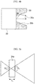
- Fig. 4a and Fig. 4b are cross sectional views showing a direction of progress of a white light according to a tilting angle of an opening of a housing.
- the white light emitted from the light conversion unit 20 can be reflected on the inside surface 30b of the housing 30a, and thereby the white light may be dissipated within the opening 30a rather than being emitted to the outside. Further, even if the light reflected on the inside surface 30b of the housing 30 is emitted to the outside, the light cannot progress straight in a horizontal direction.
- the white light emitted from the light conversion unit 20 can be reflected on the inside surface 30b of the housing 30a and the reflected light can have straightness as compared to the case described in Fig. 4a . That is to say, when the tilting angle ⁇ of the opening 30a of the housing 30 becomes smaller, the degree of straightness of the white light emitted from the opening 30a of the housing can be improved.
- the tilting angle ⁇ of the opening 30a of the housing 30 is 20° or less, the white light emitted from the light conversion unit 20 cannot be reflected on the inside surface 30b of the housing 30a.
- the tilting angle ⁇ of the opening 30a of the housing 30 may be greater than 20°, and smaller than 90°. More preferably, the tilting angle ⁇ may be in a range of 20° to 60°, but the range is not limited thereto.
- the front surface of the phosphor plate 24, which is exposed at the opening 30a of the housing, may be formed of an uneven structure. In this case, the diffusion and the scattering effect of the light may be improved by the uneven structure.
- a molding 100 which includes white silicon may be disposed between the housing 30 and the short wavelength filter 23.
- the molding 100 may be disposed to surround a side surface of the phosphor plate 24.
- the molding 100 may be rendered to include an organic material in which a silicon resin and TiO 2 are mixed, but the materials are not limited thereto.
- the molding 100 has reflexibility, thereby reflecting light emitted to the side surface of the phosphor plate 24 and directing the light to the opening 30a of the housing 30.
- the performance of the lighting device may be controlled based on a diameter of the light which is emitted from the opening 30a. For example, as a diameter of a light emitting surface of the lighting device becomes smaller, an energy density per area becomes too high and the phosphor plate 24 may be damaged. On the other hand, in order to increase the diameter of the light emitting surface of the lighting device, the diameter of the light incident region of the light which is incident on the phosphor plate 24 must become larger. That is, because there should be a sufficient distance between the light conversion unit 20 and the light source 10, the lighting device becomes larger, and hence it is difficult to miniaturize the structure of the lighting device.
- the lighting device can control a ratio (D1 : D2) of a diameter D1 of the light incident region of the light which is incident on the phosphor plate 24 and a diameter D2 of the light emitting region of the phosphor plate 24 based on a thickness of the phosphor plate 24.
- the light incident region and the light emitting region, which face each other, may respectively be disposed on a surface of the phosphor plate 24. That is, the light incident region may be disposed on a first surface (back surface) of the phosphor plate 24, which faces the light source 10.
- the light emitting region may be disposed on a second surface (front surface) of the phosphor plate 24, which faces the opening 30a at the opposite side of the first surface.
- a diameter D3 of the opening 30a of the housing 30 may also become larger as the thickness of the phosphor plate 24 increases.
- Fig. 5a and Fig. 5b are cross sectional views showing a diameter of a light incident region of light which is incident on a phosphor plate of the present invention and a diameter of a light emitting region of the phosphor plate.
- the diameter D 1 of the light incident region of the light which is incident on a first phosphor plate 24a having a first thickness T1 as shown in Fig. 5a and the diameter D1 of the light incident region of the light which is incident on a second phosphor plate 24b having a second thickness T2 which is thicker than the first thickness T1 as shown in Fig. 5b are the same, the diameters D2 of the light emitting region of the first phosphor plate 24a and the second phosphor plate 24b are different from each other. That is because the thicknesses of the first and the second phosphor plates 24a and 24b are different from each other.
- the diameter D1 of the light incident region may be adjusted based on the distance between the first phosphor plate 24a and the second phosphor plate 24b.
- the diameter D2 of the light emitting region becomes larger as the thicknesses of the first and the second phosphor plate 24a and 24b increase, the diameter D2 of the light emitting region may be controlled based on the thickness of the phosphor plate 24.
- the first and the second phosphor plates may have the ratio of the diameter of the light incident region and the diameter of the light emitting region which ranges from 1 : 3 to 1 : 9.
- the ratio of the diameter of the light incident region and the diameter of the light emitting region of the phosphor plate according to an embodiment of the present invention is shown below in Table 1.
- Table 1 shows the ratio of the diameters of the light incident region and the light emitting region based on the thickness of the phosphor plate.
- the thickness of the phosphor plate may be of 60 ⁇ m to 160 ⁇ m.
- the thickness may be a distance between the back surface (the first surface) and the front surface (the second surface) of the phosphor plate.
- the diameter of the light emitting region increases with respect to the diameter of the light incident region.
- Fig. 6a is a graph showing the diameter of the light incident region of the light which is incident on the phosphor plate
- Fig. 6b is a graph showing the diameter of the light emitting region of the phosphor plate.
- Fig. 6a and Fig. 6b show diameters of the light incident region and the light emitting region of the phosphor plate 24 having a thickness of 60 ⁇ m to 80 ⁇ m.
- the diameter of the light incident region of the phosphor plate is approximately 80 ⁇ m
- the diameter of the light emitting region of the phosphor plate is 320 ⁇ m, and hence the ratio of the diameter of the light incident region and the diameter of the light emitting region is approximately 1 : 4.
- the lighting device in order to increase the size of the light emitting region which is emitted from the lighting device, it is necessary to increase the diameter of the light incident region, and accordingly it is necessary to increase the distance between the light source 10 and the phosphor plate 24. In other words, the lighting device becomes larger, i.e. it is difficult to miniaturize the structure of the lighting device. In contrast, for miniaturizing the lighting device, if the distance between the light source 10 and the phosphor plate 24 is decreased, the light incident region of the light which is incident on the phosphor plate 24 becomes too narrow. In this case, energy is concentrated on the phosphor plate 24, and the phosphor plate 24 may be damaged.
- An embodiment according to the present invention is to prevent the above-mentioned issues, wherein due to the fact that the ratio of the diameter D1 of the light incident region and the diameter D2 of the light emitting region is different based on the thickness of the phosphor plate 24, the performance of the lighting device may be easily adjusted by controlling the light emitting region of the lighting device without limitations related to the distance between the phosphor plate 24 and the light source 10.
- a collimator 40 and a light concentrating unit 50 may be further disposed between the light source 10 and the light conversion unit 20.
- the collimator 40 is disposed closer to the light source 10 than the light concentrating unit 50.
- the collimator 40 releases a laser ray which is output from the light source 10 as a parallel light ray, and the light concentrating unit 50 concentrates the parallel light ray which is released through the collimator 40.
- the light concentrating unit 40 may refract the laser ray which passes through the collimator 40 and then allow the refracted laser ray to be incident on the light conversion unit 20.
- the light concentrating unit 50 may consist of a condensing lens, and it may refract the laser light which is incident as a parallel light toward the center of the light conversion unit 20 and allow the laser light to be incident on the light conversion unit 20.
- Fig. 7 is a block diagram of a method for producing a phosphor plate according to an embodiment of the present invention.
- a phosphor in a powder form is prepared S5.
- the phosphor may be one of yellow, green or red phosphors, and may be two or more types of phosphors that excite light which has different wavelengths, if necessary.
- the phosphor may be any one type of phosphors selected from a group consisting of a ruthenium aluminum garnet(LuAG)-based, Yttrium Aluminum Garnet(YAG)-based, silicate-based, sulfide-based, and nitride-based phosphor, but the phosphor is not limited thereto.
- the binder may be selected from at least one type of compound selected from a group consisting of tetraethyl orthosillcate (TEOS), tetramethyl orthosillcate, tetrapropyl orthosilicate, and tetraisopropyl orthosilicate, but the binder is not limited thereto.
- TEOS tetraethyl orthosillcate
- tetramethyl orthosillcate tetrapropyl orthosilicate
- tetraisopropyl orthosilicate but the binder is not limited thereto.
- the binder may also be mixed to enhance strength of the mixture.
- the compression molding may be performed at 1 to 5 tons of pressure for 1 to 10 minutes.
- cold isostatic pressing CIP is a process in which a molded product is disposed in an elastic mold immersed in liquids such as water, and the molded product is subjected to have pressure applied from all directions by applying pressure to the liquids, and through the CIP process, the molded product can be pressured to be dense and uniform in shape.
- a phosphor plate is formed S15 by performing vacuum firing by putting the compressed mixture into a firing furnace.
- a temperature and a time for performing the firing may be adjusted depending on a glass transition temperature of the phosphor.
- the vacuum firing may be performed at a temperature of 1200°C to 1800°C and a pressure of 10 -5 for 1 to 20 hours.
- a surface of the phosphor plate may be polished S20.
- a process such as dicing, drilling, and packaging may further be performed.
- the phosphor plate 24 according to the present invention may further include a ceramic powder.
- the ceramic powder may prevent being subjected to physical and chemical effects to the phosphor contained in the phosphor plate 24, and allow the phosphor to be uniformly dispersed in the phosphor plate 24.
- the ceramic powder may be at least one type of silicate-based glass powder selected from a group consisting of sodium borosilicate, aluminosilicate, zinc borosilicate, and Barium sodium silicate, but the ceramic powder is not limited thereto.
Landscapes
- Physics & Mathematics (AREA)
- Engineering & Computer Science (AREA)
- General Engineering & Computer Science (AREA)
- Spectroscopy & Molecular Physics (AREA)
- Health & Medical Sciences (AREA)
- Optics & Photonics (AREA)
- General Physics & Mathematics (AREA)
- Chemical & Material Sciences (AREA)
- Biochemistry (AREA)
- General Health & Medical Sciences (AREA)
- Analytical Chemistry (AREA)
- Immunology (AREA)
- Pathology (AREA)
- Life Sciences & Earth Sciences (AREA)
- Nuclear Medicine, Radiotherapy & Molecular Imaging (AREA)
- Crystallography & Structural Chemistry (AREA)
- Non-Portable Lighting Devices Or Systems Thereof (AREA)
- Semiconductor Lasers (AREA)
- Optical Filters (AREA)
Abstract
Description
- This application claims priority to and the benefit of Korean Patent Application No.
2016-0078012, filed on June 22, 2016 - Embodiments of the present invention are related to a phosphor plate and a lighting device including the same, specifically a lighting device which can be used in a lamp for vehicles.
- A luminous element is an element that converts electricity into light. Main luminous elements include a Light Emitting Diode(LED), a Laser Diode(LD), a laser, and the like.
- Recently, as a demand for a high efficiency, low power lighting device has increased, research on a lighting device using a laser, a LD, a high power light emitting diode, and the like as a light source is being conducted. Particularly, in a field of vehicles where energy saving has become an issue, there is an attempt to replace existing light sources used in head lamps with a laser, a LD, or a high power light emitting diode.
- Such a laser, a LD, or a high power light emitting diode emits an excitation ray which has a wavelength of 500 mm or less. If the human body is exposed to an excitation ray which has a wavelength of 500 mm or less, the excitation ray may cause harmful effects on the human body such as visual impairment, bums, and the like. Accordingly, a lighting device using a laser, a LD, or a high power light emitting diode as a light source needs to include a conversion device which converts an excitation ray from a phosphor to a visible ray, and a phosphor plate which includes a phosphor may be used as a conversion device. For example, a blue light, which is output from a low-wavelength light source emitted with a spectrum having relatively thin width, may be converted to white light by passing through a phosphor plate which includes a phosphor.
- On one hand, a performance of a lighting device may be controlled based on a diameter of a light emitting surface of the lighting device. For example, as a diameter of a light emitting surface of a lighting device becomes smaller, an energy density per area becomes too high and a phosphor plate may be damaged. On the other hand, in order to increase a diameter of a light emitting surface of a lighting device, the lighting device becomes larger, and hence it is difficult to miniaturize the structure of the lighting device.
- Embodiments of the present invention provide a lighting device including a phosphor plate which has a different ratio between a diameter of a light incident region and a diameter of a light emitting region, wherein a lighting device includes the phosphor plate.
- A phosphor plate according to an embodiment of the present invention has a light incident region on which light generated from a light source is incident and a light emitting region which converts a wavelength of the incident light and then outputs the light, wherein a ratio of a diameter of the light incident region and a diameter of the light emitting region ranges from 1 : 3 to 1 : 9.
- A lighting device according to an embodiment of the present invention includes: a light source which generates a laser ray, a light conversion unit which includes a phosphor plate having a light incident region on which the laser ray is incident and a light emitting region which outputs a converted light excited by the laser ray; and a housing which is arranged on a front surface of the light conversion unit and has an opening which exposes the light emitting region of the phosphor plate, wherein a ratio of a diameter of the light incident region of the phosphor plate and a diameter of the light emitting region of the phosphor plate ranges from 1 : 3 to 1 : 9.
- The lighting device of the invention is rendered to include a phosphor plate which has a different ratio in terms of the diameter of the light incident region and the diameter of the light emitting region, and thereby it is possible to easily adjust a performance of the lighting device by controlling the light emitting region of the lighting device without limiting a distance between the phosphor plate and the light source.
-
-
Fig. 1 is a cross sectional view of a lighting device according to an embodiment of the present invention. -
Fig. 2 is a graph showing a function of an antireflection coating and a short wavelength filter. -
Fig. 3 is a cross sectional view showing light output of a common lighting device. -
Fig. 4a andFig. 4b are cross sectional views showing a direction of progress of a white light based on a tilting angle of an opening of a housing. -
Fig. 5a andFig. 5b are cross sectional views showing a diameter of a light incident region of light which is incident on a phosphor plate of the present invention and a diameter of a light emitting region of the phosphor plate. -
Fig. 6a is a graph showing a diameter of a light incident region of light which is incident on a phosphor plate. -
Fig. 6b is a graph showing a diameter of a light emitting region of a phosphor plate. -
Fig. 7 is a block diagram of a method for producing a phosphor plate according to an embodiment of the present invention. - While the invention can allow various modifications and alternative embodiments, specific embodiments thereof are shown by way of example in the drawings and will be described hereafter. However, it should be understood that there is no intention to limit the invention to the particular embodiments disclosed, but on the contrary, the invention is to cover all modifications, equivalents, and alternatives falling within the spirit and scope of the invention.
- It will be understood that although terms including ordinal numbers such as "first," "second," etc. may be used herein to describe various elements, these elements are not limited by these terms. The terms are used to distinguish one element from another. For example, a second element could be termed a first element without departing from the teachings of the present inventive concept, and similarly a first element could be also termed a second element. The term "and/or" includes any and all combination of one or more of the related listed items.
- When an element is referred to as being "connected to" or "coupled with" another element, not only it can be directly connected or coupled to the other element, but also it can be understood that intervening elements may be present. In contrast, when an element is referred to as being "directly connected to" or "directly coupled with" another element, there are no intervening elements present.
- The terminology used herein is for the purpose of describing particular embodiments only and is not intended to limit the present inventive concept. As used herein, the singular forms "a," "an," and "the" are intended to include the plural forms as well, unless the context clearly indicates otherwise. It will be further understood that the terms "comprises" and/or "comprising," when used in this specification, specify the presence of stated features, integers, steps, operations, elements, and/or components, but do not preclude the presence or addition of one or more other features, integers, steps, operations, elements, components, and/or groups thereof.
- Unless otherwise defined, all terms including technical and scientific terms used herein have the same meaning as commonly understood by one of ordinary skill in the art to which this inventive concept belongs. It will be further understood that terms, such as those defined in commonly used dictionaries, should be interpreted as having a meaning that is consistent with their meaning in the context of the relevant art and will not be interpreted in an idealized or overly formal sense unless expressly so defined herein.
- Hereinafter, embodiments of the present invention will be described in detail with reference to the accompanying drawings, and regardless of the numbers in the drawings, the same or corresponding elements will be assigned with the same numbers and overlapping descriptions will be omitted.
- Hereinafter, a lighting device according to embodiments of the present invention will be explained in detail by referring to accompanied drawings.
-
Fig. 1 is a cross sectional view of a lighting device according to an embodiment of the present invention. - As shown in
Fig. 1 , the lighting device according to an embodiment of the present invention comprises: alight source 10; alight conversion unit 20 which is disposed in a direction that light which is output from thelight source 10 progresses and converts the output light; and ahousing 30 which includes an opening 30a formed in a light emitting region of thephosphor plate 24 and adjusts light distribution. - The
light source 10 may generate a blue laser ray which has 450 nm band of wavelength. The light generated from thelight source 10 progresses to thelight conversion unit 20. Thelight conversion unit 20 is rendered to be disposed in a direction in which the laser ray is released and to include aphosphor plate 24, so as to be able to output white light through the opening 30a of the housing by reacting the white light with the laser ray which belongs to a blue wavelength band released from thelight source 10. - The
light conversion unit 20 may transmit some part of the laser ray which belongs to the blue wavelength band released from thelight source 10, and convert the other part of the laser ray so as to form a converted light which belongs to a yellow wavelength band. Thelight conversion unit 20 may generate white light by combining the laser ray and the converted light, and the white light may be released through the opening 30a of thehousing 30. - The
light conversion unit 20 may include asubstrate 21, anantireflection coating 22, ashort wavelength filter 23 and aphosphor plate 24. - The
substrate 21 may include, but not be limited to, sapphires. Thesubstrate 21 may offer a function of radiation of heat in which heat generated from the light output from the light source passing through thelight conversion unit 20 or upon operating thelight source 10 is transferred or released. Theantireflection coating 22 which is coated onto a back surface of thesubstrate 21 is for maximizing the amount of the incident light by preventing the light from being reflected from the surface of thesubstrate 21 when the light output from thelight source 10 is incident on thesubstrate 21. - The
short wavelength filter 23 is disposed on the front surface of thesubstrate 21, and theshort wavelength filter 23 is for blocking light which belongs to a particular wavelength band. For instance, theshort wavelength filter 23 may block light which has a wavelength above 500 nm. Theshort wavelength filter 23 may be provided between thesubstrate 21 and thephosphor plate 24 and may re-reflect light in a direction towards theopening 30a, in which the light is a part of the converted light in thephosphor plate 24 and progresses in a direction towards thesubstrate 21 instead of theopening 30a. -
Fig. 2 is a graph showing the function of antireflection coating and a short wavelength filter. - As shown in
Fig. 2 , in the case of the first embodiment which includes only the substrate (referred to as 21 inFig. 1 ) and the short wavelength filter (referred to as 23 inFig. 1 ), a light which has a wavelength band of approximately between 500 nm and 800 nm is blocked, and only light which belongs to the rest of the wavelength band is transmitted. In addition, in the case of the second embodiment which includes only the substrate (referred to as 21 inFig. 1 ) and the antireflection coating (referred to as 22 inFig. 1 ), all of the light emitted from the light source (referred to as 10 inFig. 1 ) is transmitted, and in particularly, light absorption, which is caused by scattering and reflection of the light which belongs to the blue wavelength band (between 350 nm and 500 nm) generated from the light source (referred to as 10 inFig. 1 ), may be minimized. - Furthermore, in the case of the third embodiment, which includes all of the substrate (referred to as 21 in
Fig. 1 ), the short wavelength filter (referred to as 23 inFig. 1 ), and the antireflection coating (referred to as 22 inFig. 1 ), a light which has a wavelength band of approximately between 500 nm and 800 nm is blocked and at the same time a ratio of transmission of the light which belongs to the blue wavelength band may be improved. - Referring to
Fig. 1 again, thephosphor plate 24 may be provided on a surface which is in contact with thehousing 30, and may convert an absorbed light to a light which has a different wavelength and then may release the light. Thephosphor plate 24 converts the incident laser ray to a light which belongs to a yellow wavelength band so as to generate a converted light, and the converted light forms a white light by being combined with the laser ray which passes through thephosphor plate 24. Between the saidphosphor plate 24 and theshort wavelength filter 23, abonding layer 25 is further disposed, and thus thebonding layer 25 may enhance adhesion between theshort wavelength filter 23 and thephosphor plate 24. - The
housing 30 is connected to thelight conversion unit 20 at the side of the light emitting region of thephosphor plate 24, and may include theopening 30a which exposes the light emitting region of thephosphor plate 24. That is to say, thehousing 30 may expose a part of a front surface of thephosphor plate 24. Moreover, thehousing 30 may be arranged to cover a part of the front surface of thephosphor plate 24. Accordingly, the light emitted from thelight conversion unit 20 may be emitted directly to the outside through theopening 30a of the housing, or may be emitted to the outside by being reflected on aninside surface 30b of the housing which is inclined so as to have a tilting angle θ of less than 90° with respect to the light emitting region of thephosphor plate 24. -
Fig. 3 is a cross sectional view showing light output of a common lighting device. - As shown in
Fig. 3 , from among the laser rays released from the light source (referred to as 10 inFig. 1 ) and incident on thelight conversion unit 20, the laser ray which belongs to the blue wavelength band and is transmitted through thelight conversion unit 20 forms an area of light distribution a1 according to Gaussian distribution. Moreover, the converted light which is converted by the phosphor plate (referred to as 24 inFig. 1 ) forms an area of light distribution a2 according to Lambertian distribution. - That is, the white light is formed in an area in which the laser ray which belongs to the blue wavelength band according to Gaussian distribution and the yellow light according to Lambertian distribution overlap with each other, however, the light which belongs to the yellow wavelength band is released as is in an area A which is outside of the range of the Gaussian distribution. This light which belongs to the yellow wavelength band increases the overall deviation in colors in the light released from the lighting device and generates yellow-based light in the vicinity of the white light.
- Referring to
Fig. 1 again, the lighting device according to the embodiment is arranged so as to cover some part of thelight conversion unit 20, and thehousing 30 overlaps with an area which is not the light emitting region of thephosphor plate 24, and thereby a yellow-based light may be blocked. - The
opening 30a of thehousing 30 may be formed with a structure in which theopening 30a is inclined so as to have a tilting angle θ of less than 90° with respect to the light emitting region of thephosphor plate 24. Theopening 30a of thehousing 30 may have a shape in which a diameter increases along the direction of progress of the light passing through thelight conversion unit 20. That is, the diameter of theopening 30a may increase as the distance from thelight conversion unit 20 increases. In this case, the diameter of theopening 30a may be the smallest at the portion in contact with thelight conversion unit 20. Thus, the portion of theopening 30a with the smallest diameter may have the same size as a diameter of the light emitting region of thephosphor plate 24. - When the
housing 30 includes a material which has good thermal conductivity such as Al, Cu, and the like for radiating heat, thehousing 30 may be a Heat sink. In this case, the white light emitted from thelight conversion unit 20 may be reflected on theinside surface 30b, and thereby the direction of progress of the white light may be adjusted. On one hand, a metallic material or a reflecting material which can reflect light may be coated only on theinside surface 30b of the housing. However, the structure of the housing is not limited thereto. - The tilting angle θ may be set up based on an oriented angle of the white light emitted from the
light conversion unit 20. - For example, the oriented angle of the white light emitted from the
light conversion unit 20 is in a range of 150° to 170°, the tilting angle θ of theopening 30a of thehousing 30 may be in a range of 20° to 90°. - If the tilting angle θ of the
opening 30a of thehousing 30 exceeds 90°, theopening 30a of thehousing 30 may have a shape in which a diameter decreases along the direction of progress of the light passing through thelight conversion unit 20. Thus, undesirably, a sufficient amount of the white light cannot be emitted due to thehousing 30. In addition, if the tilting angle θ of theopening 30a of thehousing 30 is less than 20°, the white light emitted from thelight conversion unit 20 cannot be reflected on theinside surface 30b of thehousing 30a. Accordingly, the tilting angle θ of theopening 30a of thehousing 30 may be in a range of 20° to 90°, but the range is not limited thereto. - On one hand, the tilting angle θ of the
opening 30a of thehousing 30 may be set to control a straightness of the white light emitted from thelight conversion unit 20. -
Fig. 4a andFig. 4b are cross sectional views showing a direction of progress of a white light according to a tilting angle of an opening of a housing. - As shown in
Fig. 4a , when the tilting angle θ of theopening 30a of thehousing 30 is 90°, the white light emitted from thelight conversion unit 20 can be reflected on theinside surface 30b of thehousing 30a, and thereby the white light may be dissipated within theopening 30a rather than being emitted to the outside. Further, even if the light reflected on theinside surface 30b of thehousing 30 is emitted to the outside, the light cannot progress straight in a horizontal direction. - As shown in
Fig. 4b , when the tilting angle θ of theopening 30a of thehousing 30 is 60°, the white light emitted from thelight conversion unit 20 can be reflected on theinside surface 30b of thehousing 30a and the reflected light can have straightness as compared to the case described inFig. 4a . That is to say, when the tilting angle θ of theopening 30a of thehousing 30 becomes smaller, the degree of straightness of the white light emitted from theopening 30a of the housing can be improved. - As described above, however, when the tilting angle θ of the
opening 30a of thehousing 30 is 20° or less, the white light emitted from thelight conversion unit 20 cannot be reflected on theinside surface 30b of thehousing 30a. - Accordingly, considering the orientated angle and the straightness of the white light emitted from the
light conversion unit 20, the tilting angle θ of theopening 30a of thehousing 30 may be greater than 20°, and smaller than 90°. More preferably, the tilting angle θ may be in a range of 20° to 60°, but the range is not limited thereto. - However, although not shown in the figures, the front surface of the
phosphor plate 24, which is exposed at theopening 30a of the housing, may be formed of an uneven structure. In this case, the diffusion and the scattering effect of the light may be improved by the uneven structure. - A
molding 100 which includes white silicon may be disposed between thehousing 30 and theshort wavelength filter 23. Themolding 100 may be disposed to surround a side surface of thephosphor plate 24. Themolding 100 may be rendered to include an organic material in which a silicon resin and TiO2 are mixed, but the materials are not limited thereto. Themolding 100 has reflexibility, thereby reflecting light emitted to the side surface of thephosphor plate 24 and directing the light to theopening 30a of thehousing 30. - In general, the performance of the lighting device may be controlled based on a diameter of the light which is emitted from the
opening 30a. For example, as a diameter of a light emitting surface of the lighting device becomes smaller, an energy density per area becomes too high and thephosphor plate 24 may be damaged. On the other hand, in order to increase the diameter of the light emitting surface of the lighting device, the diameter of the light incident region of the light which is incident on thephosphor plate 24 must become larger. That is, because there should be a sufficient distance between thelight conversion unit 20 and thelight source 10, the lighting device becomes larger, and hence it is difficult to miniaturize the structure of the lighting device. - Therefore, the lighting device according to an embodiment of the present invention can control a ratio (D1 : D2) of a diameter D1 of the light incident region of the light which is incident on the
phosphor plate 24 and a diameter D2 of the light emitting region of thephosphor plate 24 based on a thickness of thephosphor plate 24. Here, the light incident region and the light emitting region, which face each other, may respectively be disposed on a surface of thephosphor plate 24. That is, the light incident region may be disposed on a first surface (back surface) of thephosphor plate 24, which faces thelight source 10. In addition, the light emitting region may be disposed on a second surface (front surface) of thephosphor plate 24, which faces theopening 30a at the opposite side of the first surface. Moreover, a diameter D3 of theopening 30a of thehousing 30 may also become larger as the thickness of thephosphor plate 24 increases. -
Fig. 5a andFig. 5b are cross sectional views showing a diameter of a light incident region of light which is incident on a phosphor plate of the present invention and a diameter of a light emitting region of the phosphor plate. - Even if the
diameter D 1 of the light incident region of the light which is incident on afirst phosphor plate 24a having a first thickness T1 as shown inFig. 5a and the diameter D1 of the light incident region of the light which is incident on asecond phosphor plate 24b having a second thickness T2 which is thicker than the first thickness T1 as shown inFig. 5b are the same, the diameters D2 of the light emitting region of thefirst phosphor plate 24a and thesecond phosphor plate 24b are different from each other. That is because the thicknesses of the first and thesecond phosphor plates - The diameter D1 of the light incident region may be adjusted based on the distance between the
first phosphor plate 24a and thesecond phosphor plate 24b. In addition, because the diameter D2 of the light emitting region becomes larger as the thicknesses of the first and thesecond phosphor plate phosphor plate 24. - In this case, the first and the second phosphor plates may have the ratio of the diameter of the light incident region and the diameter of the light emitting region which ranges from 1 : 3 to 1 : 9.
- In particular, the ratio of the diameter of the light incident region and the diameter of the light emitting region of the phosphor plate according to an embodiment of the present invention is shown below in Table 1.
- Table 1 provided below shows the ratio of the diameters of the light incident region and the light emitting region based on the thickness of the phosphor plate.
- That is, as shown in Table 1 below, when the ratio of the diameter of the light incident region and the diameter of the light emitting region is 1 : 3 to 1 : 9, at this time, the thickness of the phosphor plate may be of 60 µm to 160 µm. Here, the thickness may be a distance between the back surface (the first surface) and the front surface (the second surface) of the phosphor plate. In particular, as the thickness of the
phosphor plate 24 increases, the diameter of the light emitting region increases with respect to the diameter of the light incident region.[Table 1] Thickness of phosphor plate (µm) Diameter of light incident region (D1) : Diameter of light emitting region (D2) 60∼80 1:3∼1:4.5 80∼100 1:4.5∼1:5.5 100∼120 1:5.5∼1:6.5 120∼140 1:6.5∼1:7.5 140∼160 1:7.5∼1:9 -
Fig. 6a is a graph showing the diameter of the light incident region of the light which is incident on the phosphor plate, andFig. 6b is a graph showing the diameter of the light emitting region of the phosphor plate.Fig. 6a andFig. 6b show diameters of the light incident region and the light emitting region of thephosphor plate 24 having a thickness of 60 µm to 80 µm. - As shown in
Fig. 6a , the diameter of the light incident region of the phosphor plate is approximately 80 µm, and as shown inFig. 6b , the diameter of the light emitting region of the phosphor plate is 320 µm, and hence the ratio of the diameter of the light incident region and the diameter of the light emitting region is approximately 1 : 4. - In general, in order to increase the size of the light emitting region which is emitted from the lighting device, it is necessary to increase the diameter of the light incident region, and accordingly it is necessary to increase the distance between the
light source 10 and thephosphor plate 24. In other words, the lighting device becomes larger, i.e. it is difficult to miniaturize the structure of the lighting device. In contrast, for miniaturizing the lighting device, if the distance between thelight source 10 and thephosphor plate 24 is decreased, the light incident region of the light which is incident on thephosphor plate 24 becomes too narrow. In this case, energy is concentrated on thephosphor plate 24, and thephosphor plate 24 may be damaged. - An embodiment according to the present invention is to prevent the above-mentioned issues, wherein due to the fact that the ratio of the diameter D1 of the light incident region and the diameter D2 of the light emitting region is different based on the thickness of the
phosphor plate 24, the performance of the lighting device may be easily adjusted by controlling the light emitting region of the lighting device without limitations related to the distance between thephosphor plate 24 and thelight source 10. - Referring to
Fig. 1 again, acollimator 40 and alight concentrating unit 50 may be further disposed between thelight source 10 and thelight conversion unit 20. In this case, thecollimator 40 is disposed closer to thelight source 10 than thelight concentrating unit 50. - The
collimator 40 releases a laser ray which is output from thelight source 10 as a parallel light ray, and thelight concentrating unit 50 concentrates the parallel light ray which is released through thecollimator 40. Thelight concentrating unit 40 may refract the laser ray which passes through thecollimator 40 and then allow the refracted laser ray to be incident on thelight conversion unit 20. Thelight concentrating unit 50 may consist of a condensing lens, and it may refract the laser light which is incident as a parallel light toward the center of thelight conversion unit 20 and allow the laser light to be incident on thelight conversion unit 20. - Hereinafter, a method of producing the phosphor plate according to embodiments of the present invention will be explained in detail in the following.
-
Fig. 7 is a block diagram of a method for producing a phosphor plate according to an embodiment of the present invention. - As shown in
Fig. 7 , a phosphor in a powder form is prepared S5. The phosphor may be one of yellow, green or red phosphors, and may be two or more types of phosphors that excite light which has different wavelengths, if necessary. For example, the phosphor may be any one type of phosphors selected from a group consisting of a ruthenium aluminum garnet(LuAG)-based, Yttrium Aluminum Garnet(YAG)-based, silicate-based, sulfide-based, and nitride-based phosphor, but the phosphor is not limited thereto. - Next, the phosphors, a binder, and the like are mixed, and compression molding is performed S10 by putting the mixture into a Stainless Use Steel (SUS) mold so as to have a plate or a discus shape. The binder may be selected from at least one type of compound selected from a group consisting of tetraethyl orthosillcate (TEOS), tetramethyl orthosillcate, tetrapropyl orthosilicate, and tetraisopropyl orthosilicate, but the binder is not limited thereto. The binder may also be mixed to enhance strength of the mixture.
- The compression molding may be performed at 1 to 5 tons of pressure for 1 to 10 minutes. After the compression molding, cold isostatic pressing (CIP) may further be performed to make a high density molded product. CIP is a process in which a molded product is disposed in an elastic mold immersed in liquids such as water, and the molded product is subjected to have pressure applied from all directions by applying pressure to the liquids, and through the CIP process, the molded product can be pressured to be dense and uniform in shape.
- A phosphor plate is formed S15 by performing vacuum firing by putting the compressed mixture into a firing furnace. In this case, a temperature and a time for performing the firing may be adjusted depending on a glass transition temperature of the phosphor. For example, the vacuum firing may be performed at a temperature of 1200°C to 1800°C and a pressure of 10-5 for 1 to 20 hours.
- In order to adjust the thickness and surface roughness of the phosphor plate, a surface of the phosphor plate may be polished S20. In addition, in order to use the phosphor plate with an optical module such as a lighting device, a process such as dicing, drilling, and packaging may further be performed.
- In particular, the
phosphor plate 24 according to the present invention may further include a ceramic powder. The ceramic powder may prevent being subjected to physical and chemical effects to the phosphor contained in thephosphor plate 24, and allow the phosphor to be uniformly dispersed in thephosphor plate 24. The ceramic powder may be at least one type of silicate-based glass powder selected from a group consisting of sodium borosilicate, aluminosilicate, zinc borosilicate, and Barium sodium silicate, but the ceramic powder is not limited thereto. - The embodiments of the present invention as explained above are not limited to the accompanied embodiments and the drawings as described, and it will be apparent to those of ordinary skill in the art that it is possible to implement various substitutions, variations and modifications on the present invention without departing from the concept and scope of the present invention.
DESCRIPTION OF REFERENCE NUMERAL 10 : light source 20 : light conversion unit 21 : substrate 22 : antireflection coating 23 : short wavelength filter 24 : phosphor plate 24a : first phosphor plate 24b : second phosphor plate 25 : bonding layer 30 : housing 30a: opening 30b : inside surface 40 : collimator 50 : light concentrating unit 100 : molding
Claims (15)
- A phosphor plate (24) having a light incident region on which light generated from a light source (10) is incident and a light emitting region which converts a wavelength of the incident light and then outputs the light,
wherein a ratio of a diameter of the light incident region (D1) and a diameter of the light emitting region (D2) ranges from 1 : 3 to 1 : 9. - The phosphor plate (24) of claim 1, wherein the light incident region is disposed on a first surface of the phosphor plate (24), and the light emitting region is disposed on a second surface of the phosphor plate (24) which faces the first surface.
- The phosphor plate (24) of claim 2, wherein a distance between the first surface and the second surface is between 60µm and 160µm.
- A lighting device, comprising:a light source (10) which generates a laser ray;a light conversion unit (20) which includes a phosphor plate (24) having a light incident region on which the laser ray is incident and a light emitting region which outputs a converted light excited by the laser ray; anda housing (30) which is arranged on a front surface of the light conversion unit (20) and has an opening (30a) which exposes the light emitting region of the phosphor plate (24),wherein a ratio of a diameter of the light incident region (D1) of the phosphor plate (24) and a diameter of the light emitting region (D2) of the phosphor plate (24) ranges from 1 : 3 to 1 : 9.
- The lighting device of claim 4, wherein the light incident region is disposed on a first surface of the phosphor plate (24), and the light emitting region is disposed on a second surface of the phosphor plate (24) which faces the first surface.
- The lighting device of claim 5, wherein a distance between the first surface and the second surface is between 60µm and 160µm.
- The lighting device of claim 4, wherein the housing (30) is disposed to cover a part of a front surface of the phosphor plate (24).
- The lighting device of claim 4, wherein the housing (30) includes at least one selected from Al or Cu.
- The lighting device of claim 4, wherein a diameter of the opening (30a) of the housing (30) increases as a distance from the light conversion unit (20) increases.
- The lighting device of claim 4, wherein the smallest diameter of the opening (30a) of the housing (30) is the same as the diameter of the light emitting region (D2).
- The lighting device of claim 4, wherein the opening (30a) of the housing (30) has a structure that is inclined so as to have a tilting angle θ which is between 20° and 60° with respect to the light emitting region of the light conversion unit (20).
- The lighting device of claim 4, wherein an oriented angle of the light which passed through the light conversion unit (20) is between 150° and 170°.
- The lighting device of claim 4, wherein the light conversion unit (20) further includes:a substrate (21) disposed on a back surface of the phosphor plate (24);a short wavelength filter (23) disposed between the a front surface of the substrate (21) and the phosphor plate (24); andan antireflection coating (22) disposed on a back surface of the substrate (21).
- The lighting device of claim 13, wherein the light conversion unit (20) further includes a molding (100) which surrounds a side surface of the phosphor plate (24).
- The lighting device of claim 4,
further comprising a collimator (40) and a light concentrating unit (50) disposed between the light source (10) and the light conversion unit (20),
wherein the collimator (40) is disposed closer to the light source (10) than the light concentrating unit (50).
Applications Claiming Priority (1)
| Application Number | Priority Date | Filing Date | Title |
|---|---|---|---|
| KR1020160078012A KR20180000174A (en) | 2016-06-22 | 2016-06-22 | Phosphor plate and lighting device including the same |
Publications (2)
| Publication Number | Publication Date |
|---|---|
| EP3267095A1 true EP3267095A1 (en) | 2018-01-10 |
| EP3267095B1 EP3267095B1 (en) | 2023-08-23 |
Family
ID=59101375
Family Applications (1)
| Application Number | Title | Priority Date | Filing Date |
|---|---|---|---|
| EP17177248.6A Active EP3267095B1 (en) | 2016-06-22 | 2017-06-21 | Lighting device including a phosphor plate |
Country Status (4)
| Country | Link |
|---|---|
| US (1) | US10928035B2 (en) |
| EP (1) | EP3267095B1 (en) |
| KR (1) | KR20180000174A (en) |
| CN (1) | CN107525042A (en) |
Families Citing this family (2)
| Publication number | Priority date | Publication date | Assignee | Title |
|---|---|---|---|---|
| KR102094402B1 (en) * | 2018-08-24 | 2020-03-27 | 주식회사 케이티앤지 | Light emitting element and Aerosol generating device including the same |
| KR102168809B1 (en) | 2019-04-16 | 2020-10-22 | 동의대학교 산학협력단 | Embedded LED module converter |
Citations (7)
| Publication number | Priority date | Publication date | Assignee | Title |
|---|---|---|---|---|
| WO2012128384A1 (en) * | 2011-03-24 | 2012-09-27 | シャープ株式会社 | Light-emitting device, illumination device, and headlight |
| US8708511B2 (en) * | 2011-03-10 | 2014-04-29 | Stanley Electric Co., Ltd. | Semiconductor light source apparatus and lighting unit |
| EP2738888A2 (en) * | 2012-12-03 | 2014-06-04 | Stanley Electric Co., Ltd. | Light emitting device and vehicle lamp |
| US20140169024A1 (en) * | 2012-12-19 | 2014-06-19 | Osram Gmbh | Remote phosphor converter apparatus |
| US20150102722A1 (en) * | 2013-10-10 | 2015-04-16 | Panasonic Corporation | Wavelength conversion board and illumination device comprising the same |
| WO2015170696A1 (en) * | 2014-05-07 | 2015-11-12 | 株式会社小糸製作所 | Light source module and lighting fixture for vehicle |
| WO2017040433A1 (en) * | 2015-08-28 | 2017-03-09 | Osram Sylvania Inc. | Laser-activated remote phosphor target and system |
Family Cites Families (7)
| Publication number | Priority date | Publication date | Assignee | Title |
|---|---|---|---|---|
| KR101423456B1 (en) * | 2006-12-28 | 2014-07-29 | 서울반도체 주식회사 | A backlighting unit including a fluorescent film structure |
| US7864381B2 (en) * | 2007-03-20 | 2011-01-04 | Xerox Corporation | Document illuminator with LED-driven phosphor |
| US7618157B1 (en) * | 2008-06-25 | 2009-11-17 | Osram Sylvania Inc. | Tubular blue LED lamp with remote phosphor |
| JP2012243701A (en) * | 2011-05-24 | 2012-12-10 | Stanley Electric Co Ltd | Light source device and lighting system |
| US9235045B2 (en) * | 2013-01-16 | 2016-01-12 | Texas Instruments Incorporated | Phosphor wheel illumination using laser light reflective region |
| DE102013226639A1 (en) * | 2013-12-19 | 2015-06-25 | Osram Gmbh | Generating a Lichtabstrahlmusters in a far field |
| FR3026461B1 (en) * | 2014-09-30 | 2019-04-05 | Valeo Vision | LUMINOUS MODULE FOR LIGHTING AND / OR SIGNALING OF A MOTOR VEHICLE |
-
2016
- 2016-06-22 KR KR1020160078012A patent/KR20180000174A/en not_active Withdrawn
-
2017
- 2017-06-21 US US15/629,473 patent/US10928035B2/en active Active
- 2017-06-21 EP EP17177248.6A patent/EP3267095B1/en active Active
- 2017-06-22 CN CN201710482222.5A patent/CN107525042A/en active Pending
Patent Citations (7)
| Publication number | Priority date | Publication date | Assignee | Title |
|---|---|---|---|---|
| US8708511B2 (en) * | 2011-03-10 | 2014-04-29 | Stanley Electric Co., Ltd. | Semiconductor light source apparatus and lighting unit |
| WO2012128384A1 (en) * | 2011-03-24 | 2012-09-27 | シャープ株式会社 | Light-emitting device, illumination device, and headlight |
| EP2738888A2 (en) * | 2012-12-03 | 2014-06-04 | Stanley Electric Co., Ltd. | Light emitting device and vehicle lamp |
| US20140169024A1 (en) * | 2012-12-19 | 2014-06-19 | Osram Gmbh | Remote phosphor converter apparatus |
| US20150102722A1 (en) * | 2013-10-10 | 2015-04-16 | Panasonic Corporation | Wavelength conversion board and illumination device comprising the same |
| WO2015170696A1 (en) * | 2014-05-07 | 2015-11-12 | 株式会社小糸製作所 | Light source module and lighting fixture for vehicle |
| WO2017040433A1 (en) * | 2015-08-28 | 2017-03-09 | Osram Sylvania Inc. | Laser-activated remote phosphor target and system |
Also Published As
| Publication number | Publication date |
|---|---|
| EP3267095B1 (en) | 2023-08-23 |
| US20170370555A1 (en) | 2017-12-28 |
| KR20180000174A (en) | 2018-01-02 |
| CN107525042A (en) | 2017-12-29 |
| US10928035B2 (en) | 2021-02-23 |
Similar Documents
| Publication | Publication Date | Title |
|---|---|---|
| EP3690497B1 (en) | Optical wavelength converter and composite optical device | |
| EP2602537B1 (en) | Light source device | |
| US8872208B2 (en) | Light source device and lighting device | |
| US9082946B2 (en) | Light emitting module, a lamp, a luminaire and a display device | |
| US7819549B2 (en) | High efficiency light source using solid-state emitter and down-conversion material | |
| EP2374165B1 (en) | Led assembly | |
| US9599292B2 (en) | Light emitting module, a lamp, a luminaire and a display device | |
| US20100301353A1 (en) | Led lighting device having a conversion reflector | |
| CN104136830B (en) | conversion element and light-emitting device | |
| JP2012089316A (en) | Light source device, and lighting system | |
| JP7369724B2 (en) | Reflection color correction for phosphor lighting systems | |
| JP5709463B2 (en) | Light source device and lighting device | |
| JP7212319B2 (en) | Wavelength conversion member and light emitting device | |
| US11262046B2 (en) | Phosphor element, method for producing same, and lighting device | |
| EP3267095B1 (en) | Lighting device including a phosphor plate | |
| JP2012079989A (en) | Light source device and lighting fixture | |
| EP3286593B1 (en) | Integrating cone for an illumination device | |
| CN110494776B (en) | Wavelength conversion member and light-emitting device | |
| EP3239595B1 (en) | Lighting apparatus | |
| US11674652B2 (en) | Phosphor element, phosphor device, and illumination device | |
| US11635189B2 (en) | Phosphor element and lighting device | |
| WO2014010211A1 (en) | Light emitting module |
Legal Events
| Date | Code | Title | Description |
|---|---|---|---|
| PUAI | Public reference made under article 153(3) epc to a published international application that has entered the european phase |
Free format text: ORIGINAL CODE: 0009012 |
|
| STAA | Information on the status of an ep patent application or granted ep patent |
Free format text: STATUS: THE APPLICATION HAS BEEN PUBLISHED |
|
| AK | Designated contracting states |
Kind code of ref document: A1 Designated state(s): AL AT BE BG CH CY CZ DE DK EE ES FI FR GB GR HR HU IE IS IT LI LT LU LV MC MK MT NL NO PL PT RO RS SE SI SK SM TR |
|
| AX | Request for extension of the european patent |
Extension state: BA ME |
|
| STAA | Information on the status of an ep patent application or granted ep patent |
Free format text: STATUS: REQUEST FOR EXAMINATION WAS MADE |
|
| 17P | Request for examination filed |
Effective date: 20180710 |
|
| RBV | Designated contracting states (corrected) |
Designated state(s): AL AT BE BG CH CY CZ DE DK EE ES FI FR GB GR HR HU IE IS IT LI LT LU LV MC MK MT NL NO PL PT RO RS SE SI SK SM TR |
|
| RIC1 | Information provided on ipc code assigned before grant |
Ipc: F21S 8/10 20181130AFI20171205BHEP |
|
| RIC1 | Information provided on ipc code assigned before grant |
Ipc: F21S 8/10 20060101AFI20171205BHEP |
|
| STAA | Information on the status of an ep patent application or granted ep patent |
Free format text: STATUS: EXAMINATION IS IN PROGRESS |
|
| 17Q | First examination report despatched |
Effective date: 20200825 |
|
| REG | Reference to a national code |
Ref country code: DE Ref legal event code: R079 Free format text: PREVIOUS MAIN CLASS: F21S0008100000 Ipc: F21S0041176000 Ref country code: DE Ref legal event code: R079 Ref document number: 602017073011 Country of ref document: DE Free format text: PREVIOUS MAIN CLASS: F21S0008100000 Ipc: F21S0041176000 |
|
| RIC1 | Information provided on ipc code assigned before grant |
Ipc: F21V 9/32 20180101ALI20230123BHEP Ipc: F21V 13/14 20060101ALI20230123BHEP Ipc: F21S 41/20 20180101ALI20230123BHEP Ipc: F21S 41/176 20180101AFI20230123BHEP |
|
| GRAP | Despatch of communication of intention to grant a patent |
Free format text: ORIGINAL CODE: EPIDOSNIGR1 |
|
| STAA | Information on the status of an ep patent application or granted ep patent |
Free format text: STATUS: GRANT OF PATENT IS INTENDED |
|
| INTG | Intention to grant announced |
Effective date: 20230315 |
|
| GRAS | Grant fee paid |
Free format text: ORIGINAL CODE: EPIDOSNIGR3 |
|
| GRAA | (expected) grant |
Free format text: ORIGINAL CODE: 0009210 |
|
| STAA | Information on the status of an ep patent application or granted ep patent |
Free format text: STATUS: THE PATENT HAS BEEN GRANTED |
|
| AK | Designated contracting states |
Kind code of ref document: B1 Designated state(s): AL AT BE BG CH CY CZ DE DK EE ES FI FR GB GR HR HU IE IS IT LI LT LU LV MC MK MT NL NO PL PT RO RS SE SI SK SM TR |
|
| REG | Reference to a national code |
Ref country code: GB Ref legal event code: FG4D |
|
| REG | Reference to a national code |
Ref country code: CH Ref legal event code: EP |
|
| REG | Reference to a national code |
Ref country code: IE Ref legal event code: FG4D |
|
| REG | Reference to a national code |
Ref country code: DE Ref legal event code: R096 Ref document number: 602017073011 Country of ref document: DE |
|
| REG | Reference to a national code |
Ref country code: LT Ref legal event code: MG9D |
|
| REG | Reference to a national code |
Ref country code: NL Ref legal event code: MP Effective date: 20230823 |
|
| REG | Reference to a national code |
Ref country code: AT Ref legal event code: MK05 Ref document number: 1602970 Country of ref document: AT Kind code of ref document: T Effective date: 20230823 |
|
| PG25 | Lapsed in a contracting state [announced via postgrant information from national office to epo] |
Ref country code: GR Free format text: LAPSE BECAUSE OF FAILURE TO SUBMIT A TRANSLATION OF THE DESCRIPTION OR TO PAY THE FEE WITHIN THE PRESCRIBED TIME-LIMIT Effective date: 20231124 |
|
| PG25 | Lapsed in a contracting state [announced via postgrant information from national office to epo] |
Ref country code: IS Free format text: LAPSE BECAUSE OF FAILURE TO SUBMIT A TRANSLATION OF THE DESCRIPTION OR TO PAY THE FEE WITHIN THE PRESCRIBED TIME-LIMIT Effective date: 20231223 |
|
| PG25 | Lapsed in a contracting state [announced via postgrant information from national office to epo] |
Ref country code: SE Free format text: LAPSE BECAUSE OF FAILURE TO SUBMIT A TRANSLATION OF THE DESCRIPTION OR TO PAY THE FEE WITHIN THE PRESCRIBED TIME-LIMIT Effective date: 20230823 Ref country code: RS Free format text: LAPSE BECAUSE OF FAILURE TO SUBMIT A TRANSLATION OF THE DESCRIPTION OR TO PAY THE FEE WITHIN THE PRESCRIBED TIME-LIMIT Effective date: 20230823 Ref country code: PT Free format text: LAPSE BECAUSE OF FAILURE TO SUBMIT A TRANSLATION OF THE DESCRIPTION OR TO PAY THE FEE WITHIN THE PRESCRIBED TIME-LIMIT Effective date: 20231226 Ref country code: NO Free format text: LAPSE BECAUSE OF FAILURE TO SUBMIT A TRANSLATION OF THE DESCRIPTION OR TO PAY THE FEE WITHIN THE PRESCRIBED TIME-LIMIT Effective date: 20231123 Ref country code: NL Free format text: LAPSE BECAUSE OF FAILURE TO SUBMIT A TRANSLATION OF THE DESCRIPTION OR TO PAY THE FEE WITHIN THE PRESCRIBED TIME-LIMIT Effective date: 20230823 Ref country code: LV Free format text: LAPSE BECAUSE OF FAILURE TO SUBMIT A TRANSLATION OF THE DESCRIPTION OR TO PAY THE FEE WITHIN THE PRESCRIBED TIME-LIMIT Effective date: 20230823 Ref country code: LT Free format text: LAPSE BECAUSE OF FAILURE TO SUBMIT A TRANSLATION OF THE DESCRIPTION OR TO PAY THE FEE WITHIN THE PRESCRIBED TIME-LIMIT Effective date: 20230823 Ref country code: IS Free format text: LAPSE BECAUSE OF FAILURE TO SUBMIT A TRANSLATION OF THE DESCRIPTION OR TO PAY THE FEE WITHIN THE PRESCRIBED TIME-LIMIT Effective date: 20231223 Ref country code: HR Free format text: LAPSE BECAUSE OF FAILURE TO SUBMIT A TRANSLATION OF THE DESCRIPTION OR TO PAY THE FEE WITHIN THE PRESCRIBED TIME-LIMIT Effective date: 20230823 Ref country code: GR Free format text: LAPSE BECAUSE OF FAILURE TO SUBMIT A TRANSLATION OF THE DESCRIPTION OR TO PAY THE FEE WITHIN THE PRESCRIBED TIME-LIMIT Effective date: 20231124 Ref country code: FI Free format text: LAPSE BECAUSE OF FAILURE TO SUBMIT A TRANSLATION OF THE DESCRIPTION OR TO PAY THE FEE WITHIN THE PRESCRIBED TIME-LIMIT Effective date: 20230823 Ref country code: AT Free format text: LAPSE BECAUSE OF FAILURE TO SUBMIT A TRANSLATION OF THE DESCRIPTION OR TO PAY THE FEE WITHIN THE PRESCRIBED TIME-LIMIT Effective date: 20230823 |
|
| PG25 | Lapsed in a contracting state [announced via postgrant information from national office to epo] |
Ref country code: PL Free format text: LAPSE BECAUSE OF FAILURE TO SUBMIT A TRANSLATION OF THE DESCRIPTION OR TO PAY THE FEE WITHIN THE PRESCRIBED TIME-LIMIT Effective date: 20230823 |
|
| PG25 | Lapsed in a contracting state [announced via postgrant information from national office to epo] |
Ref country code: ES Free format text: LAPSE BECAUSE OF FAILURE TO SUBMIT A TRANSLATION OF THE DESCRIPTION OR TO PAY THE FEE WITHIN THE PRESCRIBED TIME-LIMIT Effective date: 20230823 |
|
| PG25 | Lapsed in a contracting state [announced via postgrant information from national office to epo] |
Ref country code: SM Free format text: LAPSE BECAUSE OF FAILURE TO SUBMIT A TRANSLATION OF THE DESCRIPTION OR TO PAY THE FEE WITHIN THE PRESCRIBED TIME-LIMIT Effective date: 20230823 Ref country code: RO Free format text: LAPSE BECAUSE OF FAILURE TO SUBMIT A TRANSLATION OF THE DESCRIPTION OR TO PAY THE FEE WITHIN THE PRESCRIBED TIME-LIMIT Effective date: 20230823 Ref country code: ES Free format text: LAPSE BECAUSE OF FAILURE TO SUBMIT A TRANSLATION OF THE DESCRIPTION OR TO PAY THE FEE WITHIN THE PRESCRIBED TIME-LIMIT Effective date: 20230823 Ref country code: EE Free format text: LAPSE BECAUSE OF FAILURE TO SUBMIT A TRANSLATION OF THE DESCRIPTION OR TO PAY THE FEE WITHIN THE PRESCRIBED TIME-LIMIT Effective date: 20230823 Ref country code: DK Free format text: LAPSE BECAUSE OF FAILURE TO SUBMIT A TRANSLATION OF THE DESCRIPTION OR TO PAY THE FEE WITHIN THE PRESCRIBED TIME-LIMIT Effective date: 20230823 Ref country code: CZ Free format text: LAPSE BECAUSE OF FAILURE TO SUBMIT A TRANSLATION OF THE DESCRIPTION OR TO PAY THE FEE WITHIN THE PRESCRIBED TIME-LIMIT Effective date: 20230823 Ref country code: SK Free format text: LAPSE BECAUSE OF FAILURE TO SUBMIT A TRANSLATION OF THE DESCRIPTION OR TO PAY THE FEE WITHIN THE PRESCRIBED TIME-LIMIT Effective date: 20230823 |
|
| REG | Reference to a national code |
Ref country code: DE Ref legal event code: R097 Ref document number: 602017073011 Country of ref document: DE |
|
| PG25 | Lapsed in a contracting state [announced via postgrant information from national office to epo] |
Ref country code: IT Free format text: LAPSE BECAUSE OF FAILURE TO SUBMIT A TRANSLATION OF THE DESCRIPTION OR TO PAY THE FEE WITHIN THE PRESCRIBED TIME-LIMIT Effective date: 20230823 |
|
| PLBE | No opposition filed within time limit |
Free format text: ORIGINAL CODE: 0009261 |
|
| STAA | Information on the status of an ep patent application or granted ep patent |
Free format text: STATUS: NO OPPOSITION FILED WITHIN TIME LIMIT |
|
| 26N | No opposition filed |
Effective date: 20240524 |
|
| PG25 | Lapsed in a contracting state [announced via postgrant information from national office to epo] |
Ref country code: SI Free format text: LAPSE BECAUSE OF FAILURE TO SUBMIT A TRANSLATION OF THE DESCRIPTION OR TO PAY THE FEE WITHIN THE PRESCRIBED TIME-LIMIT Effective date: 20230823 |
|
| PG25 | Lapsed in a contracting state [announced via postgrant information from national office to epo] |
Ref country code: BG Free format text: LAPSE BECAUSE OF FAILURE TO SUBMIT A TRANSLATION OF THE DESCRIPTION OR TO PAY THE FEE WITHIN THE PRESCRIBED TIME-LIMIT Effective date: 20230823 |
|
| PG25 | Lapsed in a contracting state [announced via postgrant information from national office to epo] |
Ref country code: BG Free format text: LAPSE BECAUSE OF FAILURE TO SUBMIT A TRANSLATION OF THE DESCRIPTION OR TO PAY THE FEE WITHIN THE PRESCRIBED TIME-LIMIT Effective date: 20230823 |
|
| PG25 | Lapsed in a contracting state [announced via postgrant information from national office to epo] |
Ref country code: MC Free format text: LAPSE BECAUSE OF FAILURE TO SUBMIT A TRANSLATION OF THE DESCRIPTION OR TO PAY THE FEE WITHIN THE PRESCRIBED TIME-LIMIT Effective date: 20230823 |
|
| REG | Reference to a national code |
Ref country code: CH Ref legal event code: PL |
|
| PG25 | Lapsed in a contracting state [announced via postgrant information from national office to epo] |
Ref country code: LU Free format text: LAPSE BECAUSE OF NON-PAYMENT OF DUE FEES Effective date: 20240621 |
|
| GBPC | Gb: european patent ceased through non-payment of renewal fee |
Effective date: 20240621 |
|
| PG25 | Lapsed in a contracting state [announced via postgrant information from national office to epo] |
Ref country code: IE Free format text: LAPSE BECAUSE OF NON-PAYMENT OF DUE FEES Effective date: 20240621 |
|
| PG25 | Lapsed in a contracting state [announced via postgrant information from national office to epo] |
Ref country code: CH Free format text: LAPSE BECAUSE OF NON-PAYMENT OF DUE FEES Effective date: 20240630 Ref country code: BE Free format text: LAPSE BECAUSE OF NON-PAYMENT OF DUE FEES Effective date: 20240630 |
|
| PG25 | Lapsed in a contracting state [announced via postgrant information from national office to epo] |
Ref country code: FR Free format text: LAPSE BECAUSE OF NON-PAYMENT OF DUE FEES Effective date: 20240630 |
|
| PG25 | Lapsed in a contracting state [announced via postgrant information from national office to epo] |
Ref country code: GB Free format text: LAPSE BECAUSE OF NON-PAYMENT OF DUE FEES Effective date: 20240621 |
|
| REG | Reference to a national code |
Ref country code: BE Ref legal event code: MM Effective date: 20240630 |
|
| PGFP | Annual fee paid to national office [announced via postgrant information from national office to epo] |
Ref country code: DE Payment date: 20250520 Year of fee payment: 9 |
|
| PG25 | Lapsed in a contracting state [announced via postgrant information from national office to epo] |
Ref country code: CY Free format text: LAPSE BECAUSE OF FAILURE TO SUBMIT A TRANSLATION OF THE DESCRIPTION OR TO PAY THE FEE WITHIN THE PRESCRIBED TIME-LIMIT; INVALID AB INITIO Effective date: 20170621 |
|
| PG25 | Lapsed in a contracting state [announced via postgrant information from national office to epo] |
Ref country code: HU Free format text: LAPSE BECAUSE OF FAILURE TO SUBMIT A TRANSLATION OF THE DESCRIPTION OR TO PAY THE FEE WITHIN THE PRESCRIBED TIME-LIMIT; INVALID AB INITIO Effective date: 20170621 |