EP3264530A1 - Antenna apparatus - Google Patents
Antenna apparatus Download PDFInfo
- Publication number
- EP3264530A1 EP3264530A1 EP16755671.1A EP16755671A EP3264530A1 EP 3264530 A1 EP3264530 A1 EP 3264530A1 EP 16755671 A EP16755671 A EP 16755671A EP 3264530 A1 EP3264530 A1 EP 3264530A1
- Authority
- EP
- European Patent Office
- Prior art keywords
- radome
- antenna
- gain
- thickness
- patch array
- Prior art date
- Legal status (The legal status is an assumption and is not a legal conclusion. Google has not performed a legal analysis and makes no representation as to the accuracy of the status listed.)
- Granted
Links
- 230000005855 radiation Effects 0.000 claims description 37
- 239000000758 substrate Substances 0.000 claims description 27
- 238000003491 array Methods 0.000 claims description 6
- 230000008859 change Effects 0.000 description 29
- 238000000034 method Methods 0.000 description 10
- 230000007423 decrease Effects 0.000 description 7
- 230000003247 decreasing effect Effects 0.000 description 7
- 238000010586 diagram Methods 0.000 description 2
- 238000002955 isolation Methods 0.000 description 2
- 239000000463 material Substances 0.000 description 2
- 240000001973 Ficus microcarpa Species 0.000 description 1
- 230000008901 benefit Effects 0.000 description 1
- 230000000052 comparative effect Effects 0.000 description 1
- 230000000694 effects Effects 0.000 description 1
- 230000006872 improvement Effects 0.000 description 1
- 238000009434 installation Methods 0.000 description 1
- 230000007480 spreading Effects 0.000 description 1
Images


Classifications
-
- H—ELECTRICITY
- H01—ELECTRIC ELEMENTS
- H01Q—ANTENNAS, i.e. RADIO AERIALS
- H01Q1/00—Details of, or arrangements associated with, antennas
- H01Q1/42—Housings not intimately mechanically associated with radiating elements, e.g. radome
-
- G—PHYSICS
- G01—MEASURING; TESTING
- G01S—RADIO DIRECTION-FINDING; RADIO NAVIGATION; DETERMINING DISTANCE OR VELOCITY BY USE OF RADIO WAVES; LOCATING OR PRESENCE-DETECTING BY USE OF THE REFLECTION OR RERADIATION OF RADIO WAVES; ANALOGOUS ARRANGEMENTS USING OTHER WAVES
- G01S13/00—Systems using the reflection or reradiation of radio waves, e.g. radar systems; Analogous systems using reflection or reradiation of waves whose nature or wavelength is irrelevant or unspecified
- G01S13/88—Radar or analogous systems specially adapted for specific applications
- G01S13/93—Radar or analogous systems specially adapted for specific applications for anti-collision purposes
- G01S13/931—Radar or analogous systems specially adapted for specific applications for anti-collision purposes of land vehicles
-
- G—PHYSICS
- G01—MEASURING; TESTING
- G01S—RADIO DIRECTION-FINDING; RADIO NAVIGATION; DETERMINING DISTANCE OR VELOCITY BY USE OF RADIO WAVES; LOCATING OR PRESENCE-DETECTING BY USE OF THE REFLECTION OR RERADIATION OF RADIO WAVES; ANALOGOUS ARRANGEMENTS USING OTHER WAVES
- G01S7/00—Details of systems according to groups G01S13/00, G01S15/00, G01S17/00
- G01S7/02—Details of systems according to groups G01S13/00, G01S15/00, G01S17/00 of systems according to group G01S13/00
- G01S7/03—Details of HF subsystems specially adapted therefor, e.g. common to transmitter and receiver
-
- H—ELECTRICITY
- H01—ELECTRIC ELEMENTS
- H01Q—ANTENNAS, i.e. RADIO AERIALS
- H01Q1/00—Details of, or arrangements associated with, antennas
- H01Q1/27—Adaptation for use in or on movable bodies
- H01Q1/32—Adaptation for use in or on road or rail vehicles
- H01Q1/3208—Adaptation for use in or on road or rail vehicles characterised by the application wherein the antenna is used
- H01Q1/3233—Adaptation for use in or on road or rail vehicles characterised by the application wherein the antenna is used particular used as part of a sensor or in a security system, e.g. for automotive radar, navigation systems
-
- H—ELECTRICITY
- H01—ELECTRIC ELEMENTS
- H01Q—ANTENNAS, i.e. RADIO AERIALS
- H01Q1/00—Details of, or arrangements associated with, antennas
- H01Q1/27—Adaptation for use in or on movable bodies
- H01Q1/32—Adaptation for use in or on road or rail vehicles
- H01Q1/325—Adaptation for use in or on road or rail vehicles characterised by the location of the antenna on the vehicle
- H01Q1/3258—Adaptation for use in or on road or rail vehicles characterised by the location of the antenna on the vehicle using the gutter of the vehicle; Means for clamping a whip aerial on the edge of a part of the vehicle
-
- H—ELECTRICITY
- H01—ELECTRIC ELEMENTS
- H01Q—ANTENNAS, i.e. RADIO AERIALS
- H01Q1/00—Details of, or arrangements associated with, antennas
- H01Q1/52—Means for reducing coupling between antennas; Means for reducing coupling between an antenna and another structure
- H01Q1/521—Means for reducing coupling between antennas; Means for reducing coupling between an antenna and another structure reducing the coupling between adjacent antennas
- H01Q1/525—Means for reducing coupling between antennas; Means for reducing coupling between an antenna and another structure reducing the coupling between adjacent antennas between emitting and receiving antennas
-
- H—ELECTRICITY
- H01—ELECTRIC ELEMENTS
- H01Q—ANTENNAS, i.e. RADIO AERIALS
- H01Q15/00—Devices for reflection, refraction, diffraction or polarisation of waves radiated from an antenna, e.g. quasi-optical devices
- H01Q15/02—Refracting or diffracting devices, e.g. lens, prism
- H01Q15/08—Refracting or diffracting devices, e.g. lens, prism formed of solid dielectric material
-
- H—ELECTRICITY
- H01—ELECTRIC ELEMENTS
- H01Q—ANTENNAS, i.e. RADIO AERIALS
- H01Q19/00—Combinations of primary active antenna elements and units with secondary devices, e.g. with quasi-optical devices, for giving the antenna a desired directional characteristic
- H01Q19/06—Combinations of primary active antenna elements and units with secondary devices, e.g. with quasi-optical devices, for giving the antenna a desired directional characteristic using refracting or diffracting devices, e.g. lens
-
- H—ELECTRICITY
- H01—ELECTRIC ELEMENTS
- H01Q—ANTENNAS, i.e. RADIO AERIALS
- H01Q21/00—Antenna arrays or systems
- H01Q21/06—Arrays of individually energised antenna units similarly polarised and spaced apart
- H01Q21/061—Two dimensional planar arrays
- H01Q21/065—Patch antenna array
-
- G—PHYSICS
- G01—MEASURING; TESTING
- G01S—RADIO DIRECTION-FINDING; RADIO NAVIGATION; DETERMINING DISTANCE OR VELOCITY BY USE OF RADIO WAVES; LOCATING OR PRESENCE-DETECTING BY USE OF THE REFLECTION OR RERADIATION OF RADIO WAVES; ANALOGOUS ARRANGEMENTS USING OTHER WAVES
- G01S13/00—Systems using the reflection or reradiation of radio waves, e.g. radar systems; Analogous systems using reflection or reradiation of waves whose nature or wavelength is irrelevant or unspecified
- G01S13/88—Radar or analogous systems specially adapted for specific applications
- G01S13/93—Radar or analogous systems specially adapted for specific applications for anti-collision purposes
- G01S13/931—Radar or analogous systems specially adapted for specific applications for anti-collision purposes of land vehicles
- G01S2013/9327—Sensor installation details
- G01S2013/93274—Sensor installation details on the side of the vehicles
-
- G—PHYSICS
- G01—MEASURING; TESTING
- G01S—RADIO DIRECTION-FINDING; RADIO NAVIGATION; DETERMINING DISTANCE OR VELOCITY BY USE OF RADIO WAVES; LOCATING OR PRESENCE-DETECTING BY USE OF THE REFLECTION OR RERADIATION OF RADIO WAVES; ANALOGOUS ARRANGEMENTS USING OTHER WAVES
- G01S7/00—Details of systems according to groups G01S13/00, G01S15/00, G01S17/00
- G01S7/02—Details of systems according to groups G01S13/00, G01S15/00, G01S17/00 of systems according to group G01S13/00
- G01S7/027—Constructional details of housings, e.g. form, type, material or ruggedness
- G01S7/028—Miniaturisation, e.g. surface mounted device [SMD] packaging or housings
Definitions
- the present invention relates to an antenna apparatus installed on a vehicle, and more particularly, to an antenna apparatus having a radome suitable for implementation of a predetermined directivity.
- CTA cross traffic alert
- LCDA lane change aid
- a technique of detecting obstacles in surroundings areas using a radar is employed.
- the radar radiates a radio wave in a predetermined direction, and when the radio wave is reflected by an obstacle, the obstacle is detected by receiving and processing the reflected wave.
- the radar includes a transmitting antenna that radiates a radio wave and a receiving antenna that receives a reflected wave.
- in-vehicle radar antennas used for detecting an obstacle are installed at four corners of a vehicle 10, and each antenna is installed to detect an obstacle in a predetermined range around the vehicle.
- the antenna installed on the radar have a wide directivity in a horizontal direction and a narrow directivity in a vertical direction in order to suppress unnecessary radio waves.
- a vertical direction (radiation direction) of the antenna surface has an angle of 45° from a vehicle front side on a horizontal plane and an angle of 45° from a vehicle left side as indicated by an arrow in Fig. 2 ) .
- the in-vehicle radar antenna 91 illustrated in Fig. 2 has a directivity of a range of about ⁇ 60° on the horizontal plane in order to detect obstacles around the vehicle, but it is desirable that the in-vehicle radar antenna 91 has a directivity in which a gain is high, particularly, in a vehicle front direction of -45° and a vehicle left direction of +45°. It is desirable that the antennas at the other three corners have a similar directivity.
- Patent Document 1 discloses a microwave antenna in which a directivity of a wide angle is obtained by installing an opening or a thin surface portion having a predetermined shape in a dielectric covering a front surface of an antenna opening and forming an outer corner of an antenna opening end side edge portion on a curved surface. Further, it is stated that beam control can be performed by changing conditions such as a shape, an arrangement, and the like of the dielectric.
- Patent Document 2 discloses a wide coverage radar apparatus in which a radome having a transmitting antenna and a receiving antenna accommodated therein reduces influence on a radiation characteristic of each antenna. It is stated that it is possible to reduce the influence of the radome by adjusting a thickness and a radius of curvature of a corner portion of the radome. Further, it is stated that it is possible to implement a wide angle of directivity of each antenna and improving isolation between both antennas by adjusting the thickness of the radome between the transmitting antenna and the receiving antenna. For example, it is stated that it is possible to improve a characteristic by reducing the thickness of the radome.
- Patent Document 2 a means for increasing an angle range in which a high gain is obtained and improving the isolation between the transmitting antenna and the receiving antenna is stated, but a method of increasing a gain in a specific direction and suppressing a gain outside a desired angle range is not stated.
- the invention was made to solve the above problems, and it is an object of the invention to provide an antenna apparatus which is capable of improving a gain in a specific direction, reducing an unnecessary gain in an angle range, and reducing its height.
- a first aspect of an antenna apparatus of the invention includes a circuit substrate, a patch array antenna including an element array and having a free space wavelength of ⁇ , the element array including a line of two or more patch antenna elements arranged on the circuit substrate, and a radome configured to accommodate the patch array antenna, wherein, when a plane passing through a center of the patch array antenna and being parallel to the element array and vertical to the circuit substrate is a radiation vertical surface, and an inner wall of the radome is formed to include a region in which a radome thickness in a range in which an angle with respect to a radiation vertical surface when viewed from a center of the patch array antenna is larger than -50° and smaller than +50° is smaller than a radome thickness at a position of ⁇ 50°.
- the inner wall of the radome is formed such that a radome thickness at a position intersecting with the radiation vertical surface is smallest, and a region from the position to a position at which an angle with respect to the radiation vertical surface is ⁇ 50° has a flat shape.
- the inner wall of the radome is formed such that a region from a position intersecting with the radiation vertical surface to a position at which an angle with respect to the radiation vertical surface is ⁇ 50° is a curved surface being convex toward the patch array antenna side.
- the radome is formed such that an end portion is vertical to the circuit substrate, and a distance from a center of the patch array antenna to a center of the end portion in a thickness direction is 0.85 ⁇ or more and 1.15 ⁇ or less.
- the patch array antenna includes a transmitting antenna having a line of element arrays and a receiving antenna having one or more lines of element arrays, an integrated transceiving radome including a transmitting antenna side radome portion configured to accommodate the transmitting antenna, a receiving antenna side radome portion configured to accommodate the receiving antenna, and a connecting portion connecting the transmitting antenna side radome portion with the receiving antenna side radome portion is provided, the transmitting antenna side radome portion is configured with the radome, and an interval of ⁇ /8 or more is formed between the connecting portion and the circuit substrate.
- the connecting portion when a thickness of the receiving antenna side radome portion is a reference radome thickness, the connecting portion has a thickness of 2/3 or less of the reference radome thickness.
- an antenna apparatus which is capable of improving a gain in a specific direction, reducing an unnecessary gain in an angle range, and reducing its height.
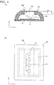
- Fig. 1 (a) is a cross-sectional view of an antenna apparatus 200 according to the present embodiment
- Fig. 1 (b) is a plane view.
- the antenna apparatus 200 includes a circuit substrate 110, a patch array antenna 130 arranged on the circuit substrate 110, and a radome 220 in which the circuit substrate 110 and the patch array antenna 130 are accommodated.
- the patch array antenna 130 includes an element array in which a line of two or more patch antenna elements 131 are arranged on one side of a circuit substrate 110.
- the patch array antenna 130 can be used as a transmitting antenna for emitting a radio wave or can be used as a receiving antenna for receiving a radio wave from the outside.
- the patch array antenna 130 is formed such that the two or more patch antenna elements 131 are arranged in a y direction illustrated in Fig. 1 , so that the patch array antenna 130 narrows a directivity in the y direction.
- the antenna apparatus 200 is installed on the vehicle, the antenna apparatus 200 is attached to the vehicle so that the ⁇ -axis is vertical, and an xz-plane is horizontal. Accordingly, the antenna apparatus 200 can have a narrow directivity in the vertical direction.
- the cross-sectional view illustrated in Fig. 1(a) is a cross-sectional view when the antenna apparatus 200 is cut along the xz plane passing through any one patch antenna element 131 of the patch array antenna 130.
- a method of forming the radome in the convex lens shape is considered as a means of narrowing the directivity in the y direction, but the thickness of the radome is increased, leading to an antenna apparatus with a high height, and thus it is difficult to implement a small-sized (compact) antenna apparatus.
- a direction vertical to the circuit substrate 110 from the center of the patch array antenna 130 is referred to as a "radiation direction.” Further, an angle from the radiation direction when viewed from the center of the patch array antenna 130 is indicated by ⁇ . Furthermore, a distance from an inner wall to an outer wall of the radome 220 when viewed from the center of the patch array antenna 130 is referred to as a "passage path length. " In the cross-sectional view illustrated in Fig. 1(a) , the radiation direction is a vertical line passing through the center of the patch array antenna 130, but in practice, the radiation direction is a vertical surface that passes through the center of the patch array antenna 130 and is parallel to an element array (a radiation vertical surface).
- the patch array antenna 130 for example, an antenna having a directivity of about ⁇ 60° from the radiation direction can be used, but in the antenna apparatus 200 of the present embodiment, a shape of the radome 220 is decided so that a directivity capable of obtaining a high gain particularly in a predetermined direction in a horizontal direction is implemented.
- a predetermined direction in which a high gain is necessary there are a direction of -45° and a direction of +45° illustrated in Fig. 2 .
- the radome 220 of the present embodiment formed so that a high gain is obtained in the directions in which the angle ⁇ is -45° and +45° will be described in detail below.
- the inner wall is formed such that a radome thickness of the radome 220 changes stepwise at a position of the angle ⁇ when viewed from the center of the patch array antenna 130.
- a radome thickness t2 on a center side further than a position at which the radome thickness changes stepwise is small, and a radome thickness t1 on an outer side than the position is large.
- Fig. 3 illustrates a change in a gain in a direction in which the angle ⁇ of the patch array antenna 130 is ⁇ 45° direction when the angle ⁇ is changed.
- the gain increases until the angle ⁇ becomes 50°, and when the angle ⁇ exceeds 50°, the gain sharply decreases.
- the change in the gain when angle ⁇ is on the positive side is illustrated, but a similar change is shown when the angle ⁇ is on the negative side. Therefore, in the antenna apparatus 200 of the present embodiment equipped with the radome 220 having the shape illustrated in Fig.
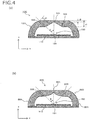
- Fig. 4 illustrates an antenna apparatus including another radome which is formed so that a high gain is obtained in the directions in which the angle ⁇ viewed from the center of the patch array antenna 130 is -45° and +45°.
- Fig. 4(a) illustrates a cross-sectional view of an antenna apparatus 100 according to a second embodiment
- Fig. 4 (b) illustrates a cross-sectional view of an antenna apparatus 300 according to a third embodiment.
- Each of a radome 120 of the antenna apparatus 100 and a radome 320 of the antenna apparatus 300 is formed so that the passage path length is large in a range of ⁇ 5° with respect to the direction in which the angle ⁇ is -45° and +45°, and a passage path length in the radiation direction is shortest.
- a central portion positioned above the patch array antenna 130 is formed to have different shapes in an outer wall and an inner wall.
- the central portion of the outer wall of the radome 120 is formed in a flat shape.
- the central portion of the inner wall of the radome 120 is formed in a characteristic shape to increase a gain in a predetermined direction.
- the inner wall of the radome 120 is formed so that a radome thickness t1 is large in a range of an angle larger than the angle ⁇ from the center of the patch antenna element 131 and decreases as it gets closer to the center of the inner wall (a position of the inner wall intersecting with the radiation direction), and a radome thickness t2 in the vertical direction at the center of the patch antenna element 131 is smallest.
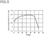
- Fig. 5 illustrates the gain of the patch array antenna 130 including the radome 120 of the present embodiment.
- Fig. 5 illustrates a change in the gain in the direction in which the angle ⁇ of the patch array antenna 130 is ⁇ 45° when the angle ⁇ is changed.
- a change similar to that of the first embodiment is shown, and the gain increases until the angle ⁇ becomes 50°, and when the angle ⁇ exceeds 50°, the gain sharply decreases.
- the inner wall of the radome 320 is formed in a curved shape from the center of the inner wall to the position in the directions in which the angle ⁇ is -50° and +50°.
- the curved shape is a curved line that is convex toward the patch array antenna 130 side at the cross-sectional view, and in practice, the curved shape is a curved surface spreading in the direction of the element array.
- the passage path length gently changes in the range of ⁇ 5° with respect to the directions in which the angle ⁇ is -45° and +45°, and the passage path length does not change greatly as in the radome 220 of the first embodiment.
- Fig. 6 illustrates a change in the gain of the patch array antenna 130 when a passage path length d1 in the direction of ⁇ 45° when viewed from the center of the patch array antenna 130 is set to be constant, and the passage path length t2 in the radiation direction is changed in the antenna apparatus 100 of the second embodiment.
- a horizontal axis illustrated in Fig. 6 indicates a ratio of the passage path length t2 in the radiation direction to the passage path length d1 in the direction of ⁇ 45°, and a vertical axis indicates the gain in the direction of 45° when viewed from the center of the patch array antenna 130.
- the gain in the direction of 45° increases as the passage path length t2 in the radiation direction decreases.
- Fig. 6 illustrates a change in the gain of the patch array antenna 130 when a passage path length d1 in the direction of ⁇ 45° when viewed from the center of the patch array antenna 130 is set to be constant, and the passage path length t2 in the radiation direction is changed in the antenna apparatus 100 of the
- the change in the gain of the antenna apparatus 100 of the second embodiment is illustrated, but the antenna apparatus 300 of the third embodiment shows a similar gain change.
- Fig. 6 that when the passage path length in the directions of -45° and +45° when viewed from the center of the patch array antenna 130 is increased, and the passage path length of the radiation direction is decreased, it is possible to obtain the high gain in the direction of ⁇ 45°.
- Fig. 7 illustrates a change in the gain of the patch array antenna 130 when a passage path length d1 in the direction of ⁇ 45° when viewed from the center of the patch array antenna 130 is set to be constant, and the passage path length t2 in the radiation direction is changed in the antenna apparatus 200 of the first embodiment.
- a horizontal axis indicates a ratio of the passage path length t2 in the radiation direction to the passage path length d1 in the direction of ⁇ 45°
- a vertical axis indicates the gain in the direction of ⁇ 45° when viewed from the center of the patch array antenna 130.
- the gain in the direction of 45° increases as the passage path length in the radiation direction decreases, but when the passage path length in the radiation direction is further decreased, the gain abruptly decreases. Therefore, when the radome thickness in the radiation direction is small, the gain may change greatly with a slight change caused by a variation in the radome thickness or the like.
- the radome thickness in the radiation direction is relatively thin, that is, about 1 mm, it is desirable that the gain hardly change even when there is a variation in the thickness. Therefore, it is more desirable to use the radome 120 of the second embodiment or the radome 320 in the third embodiment rather than the radome 220 of the first embodiment.
- Fig. 8 is a diagram illustrating a comparison of the gains in the direction of 45° when t2/d1 is 0.21 in the antenna apparatuses 100, 200, and 300 according to the embodiments. As illustrated in Fig. 8 , there is little difference in the gain in the direction of 45° between the antenna apparatus 200 of the first embodiment and the antenna apparatus 100 of the second embodiment. On the other hand, the antenna apparatus 300 of the third embodiment has a higher gain than the antenna apparatuses 100 and 200. In Fig. 8 , only the gains in the direction of +45° are compared, but the same applies to a comparison of the gains in the direction of -45°.
- the antenna apparatus 300 of the third embodiment is highest in the gain in the direction of ⁇ 45°. Accordingly, the shape of the radome 320 of the third embodiment of the antenna apparatus 300 is most preferable in terms of an improvement in the gain in the direction of ⁇ 45°.
- the inner wall of the radome is formed so that a region in which the radome thickness in the range in which the angle ⁇ viewed from the center of the patch array antenna 13 is larger than -50° and smaller than +50° is smaller than the radome thickness at the position of ⁇ 50°, and thus it is possible to reduce the unnecessary gain in the wide angle direction while improving the gain in the direction of ⁇ 45° and reduce the height.
- Fig. 9 is a cross-sectional view when an antenna apparatus 400 of the present embodiment is cut along the xz plane passing through the patch antenna element 131.
- an end portion 425 of a radome 420 is vertical to the circuit substrate 110 and further formed so as to satisfy the following conditions.
- a distance from the center of the patch array antenna 130 to the center of the end portion 425 of the radome 420 in the thickness direction is indicated by L.
- Fig. 10 illustrates a result of obtaining how the gain in the direction of 45° viewed from the center of the patch array antenna 130 is changed with the distance L.
- a free space wavelength of a radio wave radiated from the patch array antenna 130 is indicated by ⁇
- a result of normalizing the distance L using the wavelength ⁇ is a horizontal axis in Fig. 10 .
- the change in the gain in the direction of +45° is illustrated, but the same characteristic is obtained in the case of -45°.
- the radome 420 when the radome 420 is formed so that the distance L from the center of the patch array antenna 130 to the center of the end portion 425 of the radome 420 in the thickness direction is in the range of 0.85 ⁇ to 1.15 ⁇ , it is possible to obtain the high gain in the direction of 45° when viewed from the center of the patch array antenna 130.
- the radome 420 has a uniform thickness, and a region having different thicknesses is not formed even in the central portion of the radome 420 positioned above the patch array antenna 130.
- the distance L from the center of the patch antenna element 131 to the center of the end portion 425 of the radome 420 in the thickness direction satisfies the above conditions, and thus it is possible to obtain the high gain in the direction of ⁇ 45°.
- the inner wall of the central portion of the radome 420 has a similar shape as that of any one of the radomes 220, 120, and 320 of the first to third embodiments, it is possible to obtain a higher gain in the direction of ⁇ 45°.
- Fig. 11(a) is a cross-sectional view of an antenna apparatus 500 of the present embodiment
- Fig. 11(b) is a perspective view of the antenna apparatus 500.
- the antenna apparatus 500 of the present embodiment is an integrated transceiving antenna in which a transmitting antenna 530a and a receiving antenna 530b are arranged on the same circuit substrate 510.
- Each of the transmitting antenna 530a and the receiving antenna 530b is a patch array antennas formed by an element array in which a line of two or more patch antenna elements 131 are arranged in the y direction illustrated in Fig. 11 , and both antennas are arranged in parallel in the x direction.
- the transmitting antenna 530a is formed by arranging a line of element arrays, but the receiving antenna 530b may be an antenna in which one or more lines of element arrays are arranged in the x direction.
- the cross-sectional view illustrated in Fig. 11(a) is a cross-sectional view when the antenna apparatus 500 of the present embodiment is cut along the xz plane passing through the patch antenna element 131 of each of the transmitting antenna 530a and the receiving antenna 530b.
- a distance between the transmitting antenna 530a and the receiving antenna 530b it is necessary to increase a distance between the transmitting antenna 530a and the receiving antenna 530b to some extent in order to prevent the receiving antenna 530b from directly receiving a radio wave radiated from the transmitting antenna 530a.
- any one of the radomes 220, 120, 320, and 420 of the first to fourth embodiments is applied so that at least one of the transmitting antenna 530a and the receiving antenna 530b has a high gain in the direction of ⁇ 45° when viewed from the antenna center
- a radome 92 covering the transmitting antenna 530a and a radome 93 covering the receiving antenna 530b are separately installed, as illustrated in Fig. 12(a) .
- a portion of a circuit substrate 94 between the radome 92 and the radome 93 is exposed.
- An integrated transceiving radome of a related art used for the integrated transceiving antenna had a shape in which the transmitting antenna 530a and the receiving antenna 530b are covered integrally as illustrated in Fig. 12(b) .
- a shape of an inner wall above the antennas 530a and 530b is formed to be flat, and thus the high gain is not obtained in the direction of ⁇ 45° when viewed from the center of each antenna.
- an integrated transceiving radome 96 in which the same shape as the radome 120 of the second embodiment is formed in the radome inner wall above the transmitting antenna 530a as illustrated in Fig. 12 (c) may be used as the integrated transceiving radome 95 of a related art.
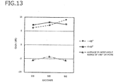
- FIG. 13 illustrates a comparison of the gain of the transmitting antenna 530a in the direction of ⁇ 45° and a gain average value of a wide angle range of ⁇ 80° or more (-180° to -80° and +80° to +180°) when the radomes 92, 95, and 96 illustrated in Fig. 12 are used.
- the integrated transceiving radome 95 of the related art when used, it is possible to reduce the gain in the wide angle range of ⁇ 80° or more, but the gain in the direction of ⁇ 45° is also low. Further, when the integrated transceiving radome 96 with the shape of the radome inner wall similar to the radome 120 of the second embodiment is used for the integrated transceiving radome of the related art, it is possible to obtain the high gain in the direction of ⁇ 45°, but the gain in the wide angle range of ⁇ 80° or more is also increased.
- the radome 92 having a similar shape as the radome 120 of the second embodiment in which only the transmitting antenna 530a is covered is used, it is possible to obtain the high gain in the direction of ⁇ 45° and reduce the gain in the wide angle range of ⁇ 80° or more.
- the radome 120 of second embodiment is applied to a radome portion 521 covering the transmitting antenna 530a and integrated with a radome portion 522 covering the receiving antenna 530b.
- any one of the radomes 220, 120, and 320 of the first to third embodiments is applied only to the radome portion 521 covering the transmitting antenna 530a, but the invention is not limited thereto and may be applied to the radome portion 522 covering the receiving antenna 530b or may be applied to both radome portions.
- Fig. 14 illustrates an integrated transceiving radome in which the radomes 92 and 93 illustrated in Fig. 12(a) are simply connected and integrated.
- the radome 92 and 93 illustrated in Fig. 12(a) are simply connected by the same material, and a space covering the transmitting antenna 530a and a space covering the receiving antenna 530b are isolated.
- a connecting portion 523 that connects the transmitting antenna side radome portion 521 with the receiving antenna side radome portion 522 is formed to have an interval of a width s between the connecting portion 523 and the circuit substrate 510.
- Fig. 15 illustrates an example of the change in the gain of the transmitting antenna 530a when the width s of the interval between the connecting portion 523 and the circuit substrate 510 is changed.
- a horizontal axis indicates a value of s/ ⁇ obtained by normalizing the interval width s between the connecting portion 523 and the circuit substrate 510 using the free space wavelength ⁇
- a vertical axis indicates the gain of the transmitting antenna 530a in the direction of ⁇ 45° and the gain average value in the wide angle range of ⁇ 80° or more.
- Fig. 15 there is a problem in that in the integrated transceiving radome 97 having no interval between the connecting portion 523 and the circuit substrate 510, a difference between the gain in the direction of -45° and the gain in the direction of +45° is increased and become asymmetric. Further, there is also a problem that the unnecessary gain in the wide angle region of ⁇ 80° or more is increased.
- the interval width s is ⁇ /8 or more in accordance with the change in the gain with respect to s/ ⁇ illustrated in Fig. 15 , and at this time, the gain in the direction of -45° and the gain in the direction of +45° are substantially symmetric, and a high value is obtained, and it is possible to reduce the unnecessary gain in the wide angle range of ⁇ 80° or more.
- FIG. 16 is a cross-sectional view of the antenna apparatus 600 of the present embodiment.
- An integrated transceiving radome 620 of an antenna apparatus 600 according to the present embodiment includes a connecting portion 623 having a different shape from the connecting portion 523 of the integrated transceiving radome 520 included in the antenna apparatus 500 of the fifth embodiment.
- the connecting portion 623 is formed to have an interval of a width s of ⁇ /8 or more between the connecting portion 623 and the circuit substrate 510, similarly to the connecting portion 523 of the fifth embodiment but has a different thickness from the connecting portion 523.
- the interval width s between the connecting portion 623 and the circuit substrate 510 has influence on the gain of the transmitting antenna 530a as described above, and the thickness of the connecting portion 623 has influence on the gain of transmitting antenna 530a.
- Fig. 17 illustrates an example of the change in the gain of the transmitting antenna 530a when the thickness of the connecting portion 623 is indicated by t, and the thickness t is changed.
- the thickness of the receiving antenna side radome portion 522 is set as a reference radome thickness t0.
- the thickness of the receiving antenna side radome portion 522 is generally decided on the basis of a 1/2 wavelength radome design technique so that a reception characteristic of the receiving antenna 530b is optimal. If a dielectric constant of a radome material used for the integrated transceiving radome 620 is indicated by ⁇ , the thickness t0 of the receiving antenna side radome portion 522 is obtained by ⁇ /2 ⁇ in the 1/2 wavelength radome design technique.
- the thickness of the connecting portion 523 of the fifth embodiment is formed to be substantially equal to the reference radome thickness t0.
- a horizontal axis indicates a value of t/t0 obtained by normalizing the thickness t of the connecting portion 623 using the reference radome thickness t0
- a vertical axis indicates the gain of the transmitting antenna 530a in the direction of ⁇ 45° and the gain average value in the wide angle range of ⁇ 80° or more.
- the thickness t of the connecting portion 623 As the thickness t of the connecting portion 623 is decreased, the unnecessary gain in the direction of ⁇ 80° is decreased. Further, it is understood that the gain in the direction of ⁇ 45° is slightly increased. It is desirable that the thickness t of the connecting portion 623 be 2/3 or less of the reference radome thickness t0 in which the unnecessary gain in the wide angle range of ⁇ 80° or more is -5 dB or less.
- the description in the present embodiment relates to an example of the antenna apparatus according to the invention, and the invention is not limited thereto.
- a detailed configuration, a detailed operation, and the like of the antenna apparatus according to the present embodiment can be appropriately changed with the scope not departing from the gist of the invention.
Abstract
Description
- The present invention relates to an antenna apparatus installed on a vehicle, and more particularly, to an antenna apparatus having a radome suitable for implementation of a predetermined directivity.
- In recent years, for example, techniques such as cross traffic alert (CTA) and lane change aid (LCA) have been developed as a technique for supporting driving of cars. In these systems, a technique of detecting obstacles in surroundings areas using a radar is employed. The radar radiates a radio wave in a predetermined direction, and when the radio wave is reflected by an obstacle, the obstacle is detected by receiving and processing the reflected wave. To this end, the radar includes a transmitting antenna that radiates a radio wave and a receiving antenna that receives a reflected wave.
- For example, as illustrated in
Fig. 2 , in-vehicle radar antennas used for detecting an obstacle are installed at four corners of avehicle 10, and each antenna is installed to detect an obstacle in a predetermined range around the vehicle. In order to detect an obstacle around the vehicle with a high degree of accuracy through the radar, it is desirable that the antenna installed on the radar have a wide directivity in a horizontal direction and a narrow directivity in a vertical direction in order to suppress unnecessary radio waves. For example, anantenna 91 installed on a front left corner of thevehicle 10 illustrated inFig. 2 is installed such that an antenna surface is erected vertically, and a vertical direction (radiation direction) of the antenna surface has an angle of 45° from a vehicle front side on a horizontal plane and an angle of 45° from a vehicle left side as indicated by an arrow inFig. 2 ) . - The in-
vehicle radar antenna 91 illustrated inFig. 2 has a directivity of a range of about ±60° on the horizontal plane in order to detect obstacles around the vehicle, but it is desirable that the in-vehicle radar antenna 91 has a directivity in which a gain is high, particularly, in a vehicle front direction of -45° and a vehicle left direction of +45°. It is desirable that the antennas at the other three corners have a similar directivity. - In order to control the directivity of the antenna, a method of using a shape of a radome covering the antenna is known. For example,
Patent Document 1 discloses a microwave antenna in which a directivity of a wide angle is obtained by installing an opening or a thin surface portion having a predetermined shape in a dielectric covering a front surface of an antenna opening and forming an outer corner of an antenna opening end side edge portion on a curved surface. Further, it is stated that beam control can be performed by changing conditions such as a shape, an arrangement, and the like of the dielectric. - Further,
Patent Document 2 discloses a wide coverage radar apparatus in which a radome having a transmitting antenna and a receiving antenna accommodated therein reduces influence on a radiation characteristic of each antenna. It is stated that it is possible to reduce the influence of the radome by adjusting a thickness and a radius of curvature of a corner portion of the radome. Further, it is stated that it is possible to implement a wide angle of directivity of each antenna and improving isolation between both antennas by adjusting the thickness of the radome between the transmitting antenna and the receiving antenna. For example, it is stated that it is possible to improve a characteristic by reducing the thickness of the radome. -
- Patent Document 1:
JP 2013-110503 A - Patent Document 2:
WO 2012/133210 - On the other hand, as a method of implementing a directivity in which a gain outside a range in which a high gain is necessary is suppressed, for example, a method of implementing a sharp directivity in a narrow angle range by causing the radome to have a convex lens shape has been known from the past. Also in
Patent Document 1, it is stated that the radome is formed in a convex lens shape in order to narrow a directivity in an orthogonal direction in which an angle is not widened. However, when the radome has the convex lens shape, the thickness of the radome is increased, and a height of an antenna apparatus is increased, and thus there is a problem in that it is difficult to implement a small-sized (compact) antenna apparatus. - Further, in
Patent Document 2, a means for increasing an angle range in which a high gain is obtained and improving the isolation between the transmitting antenna and the receiving antenna is stated, but a method of increasing a gain in a specific direction and suppressing a gain outside a desired angle range is not stated. - The invention was made to solve the above problems, and it is an object of the invention to provide an antenna apparatus which is capable of improving a gain in a specific direction, reducing an unnecessary gain in an angle range, and reducing its height.
- A first aspect of an antenna apparatus of the invention includes a circuit substrate, a patch array antenna including an element array and having a free space wavelength of λ, the element array including a line of two or more patch antenna elements arranged on the circuit substrate, and a radome configured to accommodate the patch array antenna, wherein, when a plane passing through a center of the patch array antenna and being parallel to the element array and vertical to the circuit substrate is a radiation vertical surface, and an inner wall of the radome is formed to include a region in which a radome thickness in a range in which an angle with respect to a radiation vertical surface when viewed from a center of the patch array antenna is larger than -50° and smaller than +50° is smaller than a radome thickness at a position of ±50°.
- In another aspect of the antenna apparatus of the invention, the inner wall of the radome is formed such that a radome thickness at a position intersecting with the radiation vertical surface is smallest, and a region from the position to a position at which an angle with respect to the radiation vertical surface is ±50° has a flat shape.
- In another aspect of the antenna apparatus of the invention, the inner wall of the radome is formed such that a region from a position intersecting with the radiation vertical surface to a position at which an angle with respect to the radiation vertical surface is ±50° is a curved surface being convex toward the patch array antenna side.
- In another aspect of the antenna apparatus of the invention, the radome is formed such that an end portion is vertical to the circuit substrate, and a distance from a center of the patch array antenna to a center of the end portion in a thickness direction is 0.85 λ or more and 1.15 λ or less.
- In another aspect of the antenna apparatus of the invention, the patch array antenna includes a transmitting antenna having a line of element arrays and a receiving antenna having one or more lines of element arrays, an integrated transceiving radome including a transmitting antenna side radome portion configured to accommodate the transmitting antenna, a receiving antenna side radome portion configured to accommodate the receiving antenna, and a connecting portion connecting the transmitting antenna side radome portion with the receiving antenna side radome portion is provided, the transmitting antenna side radome portion is configured with the radome, and an interval of λ/8 or more is formed between the connecting portion and the circuit substrate.
- In another aspect of the antenna apparatus of the invention, when a thickness of the receiving antenna side radome portion is a reference radome thickness, the connecting portion has a thickness of 2/3 or less of the reference radome thickness.
- According to the invention, it is possible to provide an antenna apparatus which is capable of improving a gain in a specific direction, reducing an unnecessary gain in an angle range, and reducing its height.
-
-
Fig. 1 is a cross-sectional view and a plane view illustrating a configuration of an antenna apparatus according to a first embodiment of the invention; -
Fig. 2 is a schematic diagram illustrating an installation example of an in-vehicle radar antenna; -
Fig. 3 is a graph illustrating a change in a gain in a direction in which an angle θ is ±45° with respect to an angle viewed from an antenna center of the antenna apparatus according to the first embodiment; -
Fig. 4 is a cross-sectional view illustrating a configuration of an antenna apparatus according to a second embodiment and a third embodiment of the invention; -
Fig. 5 is a graph illustrating a change in a gain in a direction in which an angle θ is ±45° with respect to an angle viewed from an antenna center of the antenna apparatus according to the second embodiment; -
Fig. 6 is a graph illustrating a change in a gain with respect to a radome thickness in a radiation direction of the antenna apparatus according to the second embodiment; -
Fig. 7 is a graph illustrating a change in a gain with respect to a radome thickness in a radiation direction of the antenna apparatus according to the first embodiment; -
Fig. 8 is a graph illustrating a comparison of gains of the antenna apparatuses according to the first to third embodiments; -
Fig. 9 is a cross-sectional view illustrating a configuration of an antenna apparatus according to a fourth embodiment of the invention; -
Fig. 10 is a graph illustrating a change in a gain with respect to a distance between a radome end portion and an antenna in the antenna apparatus according to the fourth embodiment; -
Fig. 11 is a cross-sectional view and a perspective view illustrating a configuration of an antenna apparatus according to a fifth embodiment of the invention; -
Fig. 12 is a cross-sectional view illustrating an example of a radome of an integrated transceiving antenna; -
Fig. 13 is a graph illustrating a gain comparison when radome of a comparative example is used; -
Fig. 14 is a cross-sectional view illustrating another example of the radome of the integrated transceiving antenna; -
Fig. 15 is a graph illustrating a change in a gain with respect to an interval width between a connecting portion of a radome according to the fifth embodiment and a circuit substrate; -
Fig. 16 is a cross-sectional view illustrating a configuration of an antenna apparatus according to a sixth embodiment of the invention; and -
Fig. 17 is a graph illustrating a change in a gain with respect to a thickness of a connecting portion of a radome according to the sixth embodiment. - Hereinafter, antenna apparatuses according to exemplary embodiments of the invention will be described in detail with reference to the appended drawings. Parts having the same functions are denoted by the same reference numerals for the sake of simplification of illustration and description.
- The antenna apparatus according to the first embodiment of the invention will be described with reference to
Fig. 1. Fig. 1 (a) is a cross-sectional view of anantenna apparatus 200 according to the present embodiment, andFig. 1 (b) is a plane view. Theantenna apparatus 200 includes acircuit substrate 110, apatch array antenna 130 arranged on thecircuit substrate 110, and aradome 220 in which thecircuit substrate 110 and thepatch array antenna 130 are accommodated. Thepatch array antenna 130 includes an element array in which a line of two or morepatch antenna elements 131 are arranged on one side of acircuit substrate 110. Thepatch array antenna 130 can be used as a transmitting antenna for emitting a radio wave or can be used as a receiving antenna for receiving a radio wave from the outside. - The
patch array antenna 130 is formed such that the two or morepatch antenna elements 131 are arranged in a y direction illustrated inFig. 1 , so that thepatch array antenna 130 narrows a directivity in the y direction. When theantenna apparatus 200 is installed on the vehicle, theantenna apparatus 200 is attached to the vehicle so that the γ-axis is vertical, and an xz-plane is horizontal. Accordingly, theantenna apparatus 200 can have a narrow directivity in the vertical direction. The cross-sectional view illustrated inFig. 1(a) is a cross-sectional view when theantenna apparatus 200 is cut along the xz plane passing through any onepatch antenna element 131 of thepatch array antenna 130. A method of forming the radome in the convex lens shape is considered as a means of narrowing the directivity in the y direction, but the thickness of the radome is increased, leading to an antenna apparatus with a high height, and thus it is difficult to implement a small-sized (compact) antenna apparatus. - Hereinafter, in the cross-sectional view illustrated in
Fig. 1(a) , a direction vertical to thecircuit substrate 110 from the center of thepatch array antenna 130 is referred to as a "radiation direction." Further, an angle from the radiation direction when viewed from the center of thepatch array antenna 130 is indicated by θ. Furthermore, a distance from an inner wall to an outer wall of theradome 220 when viewed from the center of thepatch array antenna 130 is referred to as a "passage path length. " In the cross-sectional view illustrated inFig. 1(a) , the radiation direction is a vertical line passing through the center of thepatch array antenna 130, but in practice, the radiation direction is a vertical surface that passes through the center of thepatch array antenna 130 and is parallel to an element array (a radiation vertical surface). - As the
patch array antenna 130, for example, an antenna having a directivity of about ±60° from the radiation direction can be used, but in theantenna apparatus 200 of the present embodiment, a shape of theradome 220 is decided so that a directivity capable of obtaining a high gain particularly in a predetermined direction in a horizontal direction is implemented. As the predetermined direction in which a high gain is necessary, there are a direction of -45° and a direction of +45° illustrated inFig. 2 . Theradome 220 of the present embodiment formed so that a high gain is obtained in the directions in which the angle θ is -45° and +45° will be described in detail below. - In the
antenna apparatus 200 illustrated inFig. 1(a) , the inner wall is formed such that a radome thickness of theradome 220 changes stepwise at a position of the angle θ when viewed from the center of thepatch array antenna 130. A radome thickness t2 on a center side further than a position at which the radome thickness changes stepwise is small, and a radome thickness t1 on an outer side than the position is large. - How the
radome 220 formed as described above affects the gain of thepatch array antenna 130 will be described with reference toFig. 3. Fig. 3 illustrates a change in a gain in a direction in which the angle θ of thepatch array antenna 130 is ±45° direction when the angle θ is changed. As can be seen fromFig. 3 , the gain increases until the angle θ becomes 50°, and when the angle θ exceeds 50°, the gain sharply decreases. InFig. 3 , the change in the gain when angle θ is on the positive side is illustrated, but a similar change is shown when the angle θ is on the negative side. Therefore, in theantenna apparatus 200 of the present embodiment equipped with theradome 220 having the shape illustrated inFig. 1 , it is understood that a high gain is obtained in a range in which the angle θ is -50° to +50°. Further, as illustrated inFig. 3 , it is possible to reduce an unnecessary gain in a wide angle exceeding, for example, ±60°. - Similarly to the
radome 220,Fig. 4 illustrates an antenna apparatus including another radome which is formed so that a high gain is obtained in the directions in which the angle θ viewed from the center of thepatch array antenna 130 is -45° and +45°.Fig. 4(a) illustrates a cross-sectional view of anantenna apparatus 100 according to a second embodiment, andFig. 4 (b) illustrates a cross-sectional view of anantenna apparatus 300 according to a third embodiment. Each of aradome 120 of theantenna apparatus 100 and aradome 320 of theantenna apparatus 300 is formed so that the passage path length is large in a range of ±5° with respect to the direction in which the angle θ is -45° and +45°, and a passage path length in the radiation direction is shortest. - In the
radome 120 illustrated inFig. 4(a) , a central portion positioned above thepatch array antenna 130 is formed to have different shapes in an outer wall and an inner wall. The central portion of the outer wall of theradome 120 is formed in a flat shape. On the other hand, the central portion of the inner wall of theradome 120 is formed in a characteristic shape to increase a gain in a predetermined direction. The inner wall of theradome 120 is formed so that a radome thickness t1 is large in a range of an angle larger than the angle θ from the center of thepatch antenna element 131 and decreases as it gets closer to the center of the inner wall (a position of the inner wall intersecting with the radiation direction), and a radome thickness t2 in the vertical direction at the center of thepatch antenna element 131 is smallest. -
Fig. 5 illustrates the gain of thepatch array antenna 130 including theradome 120 of the present embodiment.Fig. 5 illustrates a change in the gain in the direction in which the angle θ of thepatch array antenna 130 is ±45° when the angle θ is changed. In the present embodiment, a change similar to that of the first embodiment is shown, and the gain increases until the angle θ becomes 50°, and when the angle θ exceeds 50°, the gain sharply decreases. - In the
antenna apparatus 300 illustrated inFig. 4(b) , the inner wall of theradome 320 is formed in a curved shape from the center of the inner wall to the position in the directions in which the angle θ is -50° and +50°. The curved shape is a curved line that is convex toward thepatch array antenna 130 side at the cross-sectional view, and in practice, the curved shape is a curved surface spreading in the direction of the element array. In theradome 320 of the present embodiment, similarly to theradome 120 of the second embodiment, the passage path length gently changes in the range of ±5° with respect to the directions in which the angle θ is -45° and +45°, and the passage path length does not change greatly as in theradome 220 of the first embodiment. -
Fig. 6 illustrates a change in the gain of thepatch array antenna 130 when a passage path length d1 in the direction of ±45° when viewed from the center of thepatch array antenna 130 is set to be constant, and the passage path length t2 in the radiation direction is changed in theantenna apparatus 100 of the second embodiment. A horizontal axis illustrated inFig. 6 indicates a ratio of the passage path length t2 in the radiation direction to the passage path length d1 in the direction of ±45°, and a vertical axis indicates the gain in the direction of 45° when viewed from the center of thepatch array antenna 130. As can be seen fromFig. 6 , the gain in the direction of 45° increases as the passage path length t2 in the radiation direction decreases. InFig. 5 , the change in the gain of theantenna apparatus 100 of the second embodiment is illustrated, but theantenna apparatus 300 of the third embodiment shows a similar gain change. As can be seen fromFig. 6 that when the passage path length in the directions of -45° and +45° when viewed from the center of thepatch array antenna 130 is increased, and the passage path length of the radiation direction is decreased, it is possible to obtain the high gain in the direction of ±45°. The same applies to theantenna apparatus 300 of the third embodiment. -
Fig. 7 illustrates a change in the gain of thepatch array antenna 130 when a passage path length d1 in the direction of ±45° when viewed from the center of thepatch array antenna 130 is set to be constant, and the passage path length t2 in the radiation direction is changed in theantenna apparatus 200 of the first embodiment. Here, a horizontal axis indicates a ratio of the passage path length t2 in the radiation direction to the passage path length d1 in the direction of ±45°, and a vertical axis indicates the gain in the direction of ±45° when viewed from the center of thepatch array antenna 130. As can be seen fromFig. 7 , the gain in the direction of 45° increases as the passage path length in the radiation direction decreases, but when the passage path length in the radiation direction is further decreased, the gain abruptly decreases. Therefore, when the radome thickness in the radiation direction is small, the gain may change greatly with a slight change caused by a variation in the radome thickness or the like. - Accordingly, in order to obtain the high gain in the direction of ±45° from the center of the
patch array antenna 130, it is desirable to reduce the radome thickness in the radiation direction so that the passage path length of the radiation direction is decreased. However, when theradome 220 of the first embodiment is used, if the radome thickness is small, the gain may change greatly with a slight change in the radome thickness. Since the radome thickness in the radiation direction is relatively thin, that is, about 1 mm, it is desirable that the gain hardly change even when there is a variation in the thickness. Therefore, it is more desirable to use theradome 120 of the second embodiment or theradome 320 in the third embodiment rather than theradome 220 of the first embodiment. - A difference in the gain in the direction of ±45° occurring depending on the shapes of the
radomes antenna apparatus Fig. 8. Fig. 8 is a diagram illustrating a comparison of the gains in the direction of 45° when t2/d1 is 0.21 in theantenna apparatuses Fig. 8 , there is little difference in the gain in the direction of 45° between theantenna apparatus 200 of the first embodiment and theantenna apparatus 100 of the second embodiment. On the other hand, theantenna apparatus 300 of the third embodiment has a higher gain than theantenna apparatuses Fig. 8 , only the gains in the direction of +45° are compared, but the same applies to a comparison of the gains in the direction of -45°. - Accordingly, when the passage path length in the radiation direction is small, there is an advantage in that the change in the gain with respect to the variation in the radome thickness is small in the
antenna apparatus 100 of the second embodiment and theantenna apparatus 300 of the third embodiment. Further, theantenna apparatus 300 of the third embodiment is highest in the gain in the direction of ±45°. Accordingly, the shape of theradome 320 of the third embodiment of theantenna apparatus 300 is most preferable in terms of an improvement in the gain in the direction of ±45°. - According to the
antenna apparatuses - An antenna apparatus according to the fourth embodiment of the invention will be described with reference to
Fig. 9. Fig. 9 is a cross-sectional view when anantenna apparatus 400 of the present embodiment is cut along the xz plane passing through thepatch antenna element 131. In theantenna apparatus 400 of the present embodiment, anend portion 425 of aradome 420 is vertical to thecircuit substrate 110 and further formed so as to satisfy the following conditions. InFig. 9 , a distance from the center of thepatch array antenna 130 to the center of theend portion 425 of theradome 420 in the thickness direction is indicated by L.Fig. 10 illustrates a result of obtaining how the gain in the direction of 45° viewed from the center of thepatch array antenna 130 is changed with the distance L. Here, a free space wavelength of a radio wave radiated from thepatch array antenna 130 is indicated by λ, and a result of normalizing the distance L using the wavelength λ is a horizontal axis inFig. 10 . - As can be seen from
Fig. 10 , the gain in the direction of 45° from the center of thepatch antenna element 131 is highest when the distance L is substantially equal to the wavelength λ (L/λ ≈1), and the high gain is obtained in a range of L = 0.85 λ to 1.15 λ. InFig. 10 , the change in the gain in the direction of +45° is illustrated, but the same characteristic is obtained in the case of -45°. Accordingly, when theradome 420 is formed so that the distance L from the center of thepatch array antenna 130 to the center of theend portion 425 of theradome 420 in the thickness direction is in the range of 0.85 λ to 1.15 λ, it is possible to obtain the high gain in the direction of 45° when viewed from the center of thepatch array antenna 130. - In
Fig. 9 , theradome 420 has a uniform thickness, and a region having different thicknesses is not formed even in the central portion of theradome 420 positioned above thepatch array antenna 130. In this case, the distance L from the center of thepatch antenna element 131 to the center of theend portion 425 of theradome 420 in the thickness direction satisfies the above conditions, and thus it is possible to obtain the high gain in the direction of ±45°. In addition, the inner wall of the central portion of theradome 420 has a similar shape as that of any one of theradomes - An antenna apparatus according to a fifth embodiment of the invention will be described with reference to
Fig. 11. Fig. 11(a) is a cross-sectional view of anantenna apparatus 500 of the present embodiment, andFig. 11(b) is a perspective view of theantenna apparatus 500. Theantenna apparatus 500 of the present embodiment is an integrated transceiving antenna in which a transmittingantenna 530a and a receivingantenna 530b are arranged on thesame circuit substrate 510. - Each of the transmitting
antenna 530a and the receivingantenna 530b is a patch array antennas formed by an element array in which a line of two or morepatch antenna elements 131 are arranged in the y direction illustrated inFig. 11 , and both antennas are arranged in parallel in the x direction. The transmittingantenna 530a is formed by arranging a line of element arrays, but the receivingantenna 530b may be an antenna in which one or more lines of element arrays are arranged in the x direction. The cross-sectional view illustrated inFig. 11(a) is a cross-sectional view when theantenna apparatus 500 of the present embodiment is cut along the xz plane passing through thepatch antenna element 131 of each of the transmittingantenna 530a and the receivingantenna 530b. - In the integrated transceiving antenna, it is necessary to increase a distance between the transmitting
antenna 530a and the receivingantenna 530b to some extent in order to prevent the receivingantenna 530b from directly receiving a radio wave radiated from the transmittingantenna 530a. To this end, when any one of theradomes antenna 530a and the receivingantenna 530b has a high gain in the direction of ±45° when viewed from the antenna center, aradome 92 covering the transmittingantenna 530a and aradome 93 covering the receivingantenna 530b are separately installed, as illustrated inFig. 12(a) . Thus, a portion of acircuit substrate 94 between theradome 92 and theradome 93 is exposed. - An integrated transceiving radome of a related art used for the integrated transceiving antenna had a shape in which the transmitting
antenna 530a and the receivingantenna 530b are covered integrally as illustrated inFig. 12(b) . In anintegrated transceiving radome 95 of a related art, a shape of an inner wall above theantennas antenna 530a in the direction of ±45°, for example, anintegrated transceiving radome 96 in which the same shape as theradome 120 of the second embodiment is formed in the radome inner wall above the transmittingantenna 530a as illustrated inFig. 12 (c) may be used as theintegrated transceiving radome 95 of a related art. - However, it is possible to improve the gain of the transmitting
antenna 530a in the direction of ±45° using the integratedtransceiving radome 96, but there is a problem in that the high gain is obtained even in a wide angle direction in which the gain is desired to be reduced, for example, in a wide angle direction of ±80° or more. On the other hand, in theradome 92 illustrated inFig. 12 (a) , it is possible to obtain the high gain of the transmittingantenna 530a in the direction of ±45° and reduce the gain in the wide angle direction of ±80° or more.Fig. 13 illustrates a comparison of the gain of the transmittingantenna 530a in the direction of ±45° and a gain average value of a wide angle range of ±80° or more (-180° to -80° and +80° to +180°) when theradomes Fig. 12 are used. - As illustrated in
Fig. 13 , when theintegrated transceiving radome 95 of the related art is used, it is possible to reduce the gain in the wide angle range of ±80° or more, but the gain in the direction of ±45° is also low. Further, when theintegrated transceiving radome 96 with the shape of the radome inner wall similar to theradome 120 of the second embodiment is used for the integrated transceiving radome of the related art, it is possible to obtain the high gain in the direction of ±45°, but the gain in the wide angle range of ±80° or more is also increased. On the other hand, when theradome 92 having a similar shape as theradome 120 of the second embodiment in which only the transmittingantenna 530a is covered is used, it is possible to obtain the high gain in the direction of ±45° and reduce the gain in the wide angle range of ±80° or more. - In an
integrated transceiving radome 520 of the present embodiment illustrated inFig. 11 , theradome 120 of second embodiment is applied to aradome portion 521 covering the transmittingantenna 530a and integrated with aradome portion 522 covering the receivingantenna 530b. Here, any one of theradomes radome portion 521 covering the transmittingantenna 530a, but the invention is not limited thereto and may be applied to theradome portion 522 covering the receivingantenna 530b or may be applied to both radome portions. -
Fig. 14 illustrates an integrated transceiving radome in which theradomes Fig. 12(a) are simply connected and integrated. In anintegrated transceiving radome 97 illustrated inFig. 14 , theradome Fig. 12(a) are simply connected by the same material, and a space covering the transmittingantenna 530a and a space covering the receivingantenna 530b are isolated. Even when theintegrated transceiving radome 97 is used, there arises a problem in that the gain of the transmittingantenna 530a in the direction of ±45° is decreased, and the unnecessary gain in the wide angle direction is increased. - In this regard, in an
integrated transceiving radome 520 of theantenna apparatus 500 of the present embodiment illustrated inFig. 11 , a connectingportion 523 that connects the transmitting antennaside radome portion 521 with the receiving antennaside radome portion 522 is formed to have an interval of a width s between the connectingportion 523 and thecircuit substrate 510.Fig. 15 illustrates an example of the change in the gain of the transmittingantenna 530a when the width s of the interval between the connectingportion 523 and thecircuit substrate 510 is changed.Fig. 15 illustrates a change in each gain when the interval width s is changed where a horizontal axis indicates a value of s/ λ obtained by normalizing the interval width s between the connectingportion 523 and thecircuit substrate 510 using the free space wavelength λ, and a vertical axis indicates the gain of the transmittingantenna 530a in the direction of ±45° and the gain average value in the wide angle range of ±80° or more. - In
Fig. 15 , when s/λ = 0, that is, when s = 0, it corresponds to theintegrated transceiving radome 97 illustrated inFig. 14 . As can be seen fromFig. 15 , there is a problem in that in theintegrated transceiving radome 97 having no interval between the connectingportion 523 and thecircuit substrate 510, a difference between the gain in the direction of -45° and the gain in the direction of +45° is increased and become asymmetric. Further, there is also a problem that the unnecessary gain in the wide angle region of ±80° or more is increased. On the other hand, when an interval is formed between the connectingportion 523 and thecircuit substrate 510 to increase the width s, the gain in the direction of -45° and the gain in the direction of +45° are substantially equal, so that symmetry is obtained, and also the unnecessary gain in the wide angle region of ±80° or more is decreased. - It is desirable to set the interval width s to be λ/8 or more in accordance with the change in the gain with respect to s/λ illustrated in
Fig. 15 , and at this time, the gain in the direction of -45° and the gain in the direction of +45° are substantially symmetric, and a high value is obtained, and it is possible to reduce the unnecessary gain in the wide angle range of ±80° or more. - An antenna apparatus according to the sixth embodiment of the invention will be described with reference to
Fig. 16. Fig. 16 is a cross-sectional view of theantenna apparatus 600 of the present embodiment. Anintegrated transceiving radome 620 of anantenna apparatus 600 according to the present embodiment includes a connectingportion 623 having a different shape from the connectingportion 523 of theintegrated transceiving radome 520 included in theantenna apparatus 500 of the fifth embodiment. The connectingportion 623 is formed to have an interval of a width s of λ/8 or more between the connectingportion 623 and thecircuit substrate 510, similarly to the connectingportion 523 of the fifth embodiment but has a different thickness from the connectingportion 523. - In the connecting
portion 623 connecting the transmitting antennaside radome portion 521 with the receiving antennaside radome portion 522, the interval width s between the connectingportion 623 and thecircuit substrate 510 has influence on the gain of the transmittingantenna 530a as described above, and the thickness of the connectingportion 623 has influence on the gain of transmittingantenna 530a.Fig. 17 illustrates an example of the change in the gain of the transmittingantenna 530a when the thickness of the connectingportion 623 is indicated by t, and the thickness t is changed. Here, the thickness of the receiving antennaside radome portion 522 is set as a reference radome thickness t0. - The thickness of the receiving antenna
side radome portion 522 is generally decided on the basis of a 1/2 wavelength radome design technique so that a reception characteristic of the receivingantenna 530b is optimal. If a dielectric constant of a radome material used for theintegrated transceiving radome 620 is indicated by ε, the thickness t0 of the receiving antennaside radome portion 522 is obtained by λ/2√ε in the 1/2 wavelength radome design technique. The thickness of the connectingportion 523 of the fifth embodiment is formed to be substantially equal to the reference radome thickness t0. - In
Fig. 17 , a horizontal axis indicates a value of t/t0 obtained by normalizing the thickness t of the connectingportion 623 using the reference radome thickness t0, and a vertical axis indicates the gain of the transmittingantenna 530a in the direction of ±45° and the gain average value in the wide angle range of ±80° or more. As can be seen fromFig. 17 , as the thickness t of the connectingportion 623 is decreased, the unnecessary gain in the direction of ±80° is decreased. Further, it is understood that the gain in the direction of ±45° is slightly increased. It is desirable that the thickness t of the connectingportion 623 be 2/3 or less of the reference radome thickness t0 in which the unnecessary gain in the wide angle range of ±80° or more is -5 dB or less. - As described above, in all the antenna apparatuses according to the first to sixth embodiments of this invention, it is possible to increase the gain in the direction of ±45° in which the high gain is necessary and decrease the unnecessary gain in the wide angle direction, and it is possible to implement the low-height (compact) radome.
- The description in the present embodiment relates to an example of the antenna apparatus according to the invention, and the invention is not limited thereto. A detailed configuration, a detailed operation, and the like of the antenna apparatus according to the present embodiment can be appropriately changed with the scope not departing from the gist of the invention.
-
- 100, 200, 300, 400, 500, 600 antenna apparatus
- 110, 510 circuit substrate
- 120, 220, 320, 420 radome
- 121, 221, 321 thin wall point
- 122, 123, 222, 223, 322, 323 thick wall point
- 130 patch array antenna
- 131 patch antenna element
- 324 sidewall
- 425 end portion
- 520, 620 integrated transceiving radome
- 521 transmitting antenna side radome portion
- 522 receiving antenna side radome portion
- 523, 623 connecting portion
- 530a transmitting antenna
- 530b receiving antenna
Claims (6)
- An antenna apparatus, comprising:a circuit substrate;a patch array antenna including an element array andhaving a free space wavelength of λ, the element array including a line of two or more patch antenna elements arranged on the circuit substrate; anda radome configured to accommodate the patch array antenna,wherein, when a plane passing through a center of the patch array antenna and being parallel to the element array andvertical to the circuit substrate is a radiation vertical surface,an inner wall of the radome is formed to include a region in which a radome thickness in a range in which an angle with respect to a radiation vertical surface when viewed from a center of the patch array antenna is larger than -50° and smaller than +50° is smaller than a radome thickness at a position of ±50°.
- The antenna apparatus according to claim 1,
wherein the inner wall of the radome is formed such that a radome thickness at a position intersecting with the radiation vertical surface is smallest, and a region from the position to a position at which an angle with respect to the radiation vertical surface is ±50° has a flat shape. - The antenna apparatus according to claim 1,
wherein the inner wall of the radome is formed in a curved shape being convex toward the patch array antenna side from a position intersecting with the radiation vertical surface to a position at which an angle with respect to the radiation vertical surface is ±50°. - The antenna apparatus according to any one of claims 1 to 3,
wherein the radome is formed such that an end portion of the radome is vertical to the circuit substrate, and a distance from a center of the patch array antenna to a center of the end portion in a thickness direction is 0.85 λ or more and 1.15 λ or less. - The antenna apparatus according to any one of claims 1 to 4,
wherein the patch array antenna includes a transmitting antenna having a line of element arrays and a receiving antenna having one or more lines of element arrays, an integrated transceiving radome including a transmitting antenna side radome portion configured to accommodate the transmitting antenna, a receiving antenna side radome portion configured to accommodate the receiving antenna, and a connecting portion connecting the transmitting antenna side radome portion with the receiving antenna side radome portion is provided, the transmitting antenna side radome portion is configured with the radome, and
an interval of λ/8 or more is formed between the connecting portion and the circuit substrate. - The antenna apparatus according to claim 5,
wherein, when a thickness of the receiving antenna side radome portion is a reference radome thickness, the connecting portion has a thickness of 2/3 or less of the reference radome thickness.
Applications Claiming Priority (2)
| Application Number | Priority Date | Filing Date | Title |
|---|---|---|---|
| JP2015037828 | 2015-02-27 | ||
| PCT/JP2016/055751 WO2016136927A1 (en) | 2015-02-27 | 2016-02-26 | Antenna apparatus |
Publications (3)
| Publication Number | Publication Date |
|---|---|
| EP3264530A1 true EP3264530A1 (en) | 2018-01-03 |
| EP3264530A4 EP3264530A4 (en) | 2018-10-31 |
| EP3264530B1 EP3264530B1 (en) | 2022-02-09 |
Family
ID=56789530
Family Applications (1)
| Application Number | Title | Priority Date | Filing Date |
|---|---|---|---|
| EP16755671.1A Active EP3264530B1 (en) | 2015-02-27 | 2016-02-26 | Antenna apparatus |
Country Status (5)
| Country | Link |
|---|---|
| US (1) | US10680318B2 (en) |
| EP (1) | EP3264530B1 (en) |
| JP (1) | JP6640182B2 (en) |
| CN (1) | CN107004960B (en) |
| WO (1) | WO2016136927A1 (en) |
Families Citing this family (29)
| Publication number | Priority date | Publication date | Assignee | Title |
|---|---|---|---|---|
| CN107667450A (en) * | 2015-05-21 | 2018-02-06 | 康普技术有限责任公司 | Sectional antenna cover |
| JP6510439B2 (en) * | 2016-02-23 | 2019-05-08 | 株式会社Soken | Antenna device |
| US10461413B2 (en) * | 2016-09-19 | 2019-10-29 | Peraso Technologies Inc. | Enclosure for millimeter-wave antenna system |
| JP6799808B2 (en) * | 2016-11-07 | 2020-12-16 | パナソニックIpマネジメント株式会社 | Radio sensor and lighting equipment |
| JP6840564B2 (en) * | 2017-02-21 | 2021-03-10 | 日本無線株式会社 | Planar antenna device |
| JP6738763B2 (en) * | 2017-04-18 | 2020-08-12 | 株式会社Soken | Radar equipment |
| US10320055B2 (en) * | 2017-04-28 | 2019-06-11 | DISH Technologies L.L.C. | Radio frequency antenna for short range communications |
| JP6838250B2 (en) * | 2017-06-05 | 2021-03-03 | 日立Astemo株式会社 | Antennas, array antennas, radar devices and in-vehicle systems |
| WO2019067474A1 (en) * | 2017-09-26 | 2019-04-04 | Trak Microwave Corporation | Low profile beam steering antenna with integrated divergent lens |
| DE102017218103A1 (en) * | 2017-10-11 | 2019-04-11 | Continental Automotive Gmbh | Housing for a radar sensor and device for transmitting electrical energy by means of inductive coupling |
| JP6852005B2 (en) * | 2018-03-08 | 2021-03-31 | 古河電気工業株式会社 | Structure attached to radar device |
| JP7065401B2 (en) * | 2018-04-27 | 2022-05-12 | パナソニックIpマネジメント株式会社 | Radio sensor and mobile |
| JP7145665B2 (en) * | 2018-07-10 | 2022-10-03 | 古河電気工業株式会社 | Antenna device and radar device |
| CN111200191B (en) * | 2018-11-16 | 2022-02-18 | 荷兰移动驱动器公司 | Antenna structure and wireless communication device with same |
| JP7163209B2 (en) * | 2019-02-06 | 2022-10-31 | 日立Astemo株式会社 | radar equipment |
| JP6563159B6 (en) * | 2019-03-07 | 2019-10-23 | 三菱電機株式会社 | Antenna device |
| US11543511B2 (en) * | 2019-03-11 | 2023-01-03 | Panasonic Intellectual Property Management Co., Ltd. | Radar apparatus and vehicle |
| JP7289070B2 (en) * | 2019-03-11 | 2023-06-09 | パナソニックIpマネジメント株式会社 | radar equipment and vehicles |
| WO2020230694A1 (en) * | 2019-05-16 | 2020-11-19 | ソニー株式会社 | Mobile body |
| JP7208102B2 (en) * | 2019-05-17 | 2023-01-18 | 株式会社デンソーテン | antenna device |
| JP7244361B2 (en) * | 2019-05-27 | 2023-03-22 | 株式会社デンソーテン | antenna device |
| US11264712B2 (en) | 2019-06-21 | 2022-03-01 | Veoneer Us, Inc. | Radar sensor with radome having trenches for reducing coupling between transmit and receive antennas |
| JP7242441B2 (en) * | 2019-06-24 | 2023-03-20 | 日立Astemo株式会社 | radar equipment |
| JP2021061502A (en) * | 2019-10-04 | 2021-04-15 | ソニーセミコンダクタソリューションズ株式会社 | Antenna device and wireless communication device |
| IL271269A (en) * | 2019-12-09 | 2021-06-30 | Arbe Robotics Ltd | Radome for automotive radar patch antenna |
| JP2021113688A (en) * | 2020-01-16 | 2021-08-05 | 本田技研工業株式会社 | Molded product for vehicles |
| CN111430901B (en) * | 2020-01-17 | 2022-04-12 | 上海阿莱德实业股份有限公司 | Antenna housing integrating antennas for 5G base station and preparation method thereof |
| FR3111711A1 (en) * | 2020-06-19 | 2021-12-24 | Valeo Vision | Vehicle assembly including radar sensor |
| EP4315511A1 (en) * | 2021-07-16 | 2024-02-07 | Samsung Electronics Co., Ltd. | Wide scanning patch antenna array |
Family Cites Families (29)
| Publication number | Priority date | Publication date | Assignee | Title |
|---|---|---|---|---|
| DE4412770A1 (en) * | 1994-04-13 | 1995-10-19 | Siemens Ag | Microwave lens aerial for car distance warning radar |
| JP3786497B2 (en) * | 1997-06-13 | 2006-06-14 | 富士通株式会社 | Semiconductor module with built-in antenna element |
| JP2000101336A (en) * | 1998-09-28 | 2000-04-07 | Mitsubishi Electric Corp | Dielectric lens |
| JP2000174543A (en) * | 1998-12-01 | 2000-06-23 | Nippon Signal Co Ltd:The | Antenna system and automatic train controller |
| DE19961774A1 (en) * | 1999-12-21 | 2001-07-12 | Bosch Gmbh Robert | Device for setting a directional beam system |
| DE19963004A1 (en) * | 1999-12-24 | 2001-06-28 | Bosch Gmbh Robert | Vehicle radar system, e.g. for adaptive cruise control has dielectric body in beam path heated by directly contacting electrically-conducting tracks of material with positive temperature coefficient |
| US6947003B2 (en) * | 2002-06-06 | 2005-09-20 | Oki Electric Industry Co., Ltd. | Slot array antenna |
| JP2006105866A (en) * | 2004-10-07 | 2006-04-20 | Matsushita Electric Ind Co Ltd | Radar device |
| JP4065268B2 (en) * | 2004-11-15 | 2008-03-19 | アンリツ株式会社 | Automotive antenna |
| JP2006145399A (en) * | 2004-11-19 | 2006-06-08 | Matsushita Electric Ind Co Ltd | Vehicle-mounted radar system |
| JP2007201868A (en) * | 2006-01-27 | 2007-08-09 | Mitsubishi Electric Corp | Transmission/reception antenna for radar equipment |
| JP4557177B2 (en) * | 2006-09-04 | 2010-10-06 | トヨタ自動車株式会社 | Antenna device |
| DE102007058236A1 (en) * | 2007-12-04 | 2009-06-10 | Robert Bosch Gmbh | Bistatic array antenna and method |
| US20100039346A1 (en) * | 2008-04-21 | 2010-02-18 | Northrop Grumman Corporation | Asymmetric Radome For Phased Antenna Arrays |
| JP2009278501A (en) * | 2008-05-16 | 2009-11-26 | Yokowo Co Ltd | Housing for antenna |
| JP5603636B2 (en) * | 2010-04-09 | 2014-10-08 | 古野電気株式会社 | Radome, antenna device, and radar device |
| JP5555087B2 (en) | 2010-07-30 | 2014-07-23 | 株式会社豊田中央研究所 | Radar equipment |
| JP5307092B2 (en) * | 2010-08-18 | 2013-10-02 | シャープ株式会社 | ANTENNA DEVICE AND ELECTRIC DEVICE HAVING THE SAME |
| WO2012133210A1 (en) | 2011-03-31 | 2012-10-04 | 古河電気工業株式会社 | Wide-coverage radar device |
| US8810468B2 (en) * | 2011-06-27 | 2014-08-19 | Raytheon Company | Beam shaping of RF feed energy for reflector-based antennas |
| JP5789492B2 (en) | 2011-11-18 | 2015-10-07 | 新日本無線株式会社 | Microwave antenna |
| US20140091969A1 (en) * | 2012-10-02 | 2014-04-03 | Delphi Technologies, Inc. | Radome for a radar sensor assembly |
| EP2993485A4 (en) * | 2013-04-30 | 2017-03-08 | Furukawa Electric Co., Ltd. | Radar apparatus |
| JP6347424B2 (en) * | 2013-06-25 | 2018-06-27 | パナソニックIpマネジメント株式会社 | Wireless module |
| JP6498931B2 (en) * | 2014-12-25 | 2019-04-10 | 株式会社Soken | Radar device and cover member |
| JP6487208B2 (en) * | 2014-12-26 | 2019-03-20 | 株式会社Soken | Radar device and cover member |
| JP6440123B2 (en) * | 2015-05-19 | 2018-12-19 | パナソニックIpマネジメント株式会社 | Antenna device, radio communication device, and radar device |
| KR102308250B1 (en) * | 2015-08-06 | 2021-10-05 | 엘지이노텍 주식회사 | Radome and radar apparatus for vehicle having the same |
| US10263332B2 (en) * | 2017-09-18 | 2019-04-16 | Apple Inc. | Antenna arrays with etched substrates |
-
2016
- 2016-02-26 EP EP16755671.1A patent/EP3264530B1/en active Active
- 2016-02-26 CN CN201680004004.4A patent/CN107004960B/en active Active
- 2016-02-26 WO PCT/JP2016/055751 patent/WO2016136927A1/en active Application Filing
- 2016-02-26 JP JP2017502500A patent/JP6640182B2/en active Active
-
2017
- 2017-08-18 US US15/681,209 patent/US10680318B2/en active Active
Also Published As
| Publication number | Publication date |
|---|---|
| US20170346177A1 (en) | 2017-11-30 |
| WO2016136927A1 (en) | 2016-09-01 |
| US10680318B2 (en) | 2020-06-09 |
| CN107004960B (en) | 2020-08-25 |
| JP6640182B2 (en) | 2020-02-05 |
| CN107004960A (en) | 2017-08-01 |
| JPWO2016136927A1 (en) | 2017-12-07 |
| EP3264530B1 (en) | 2022-02-09 |
| EP3264530A4 (en) | 2018-10-31 |
Similar Documents
| Publication | Publication Date | Title |
|---|---|---|
| US10680318B2 (en) | Antenna apparatus | |
| CN105762489B (en) | Radar antenna assembly with panoramic detection | |
| EP3096400B1 (en) | Antenna device, wireless communication apparatus, and radar apparatus | |
| EP3522297B1 (en) | Wide angle coverage antenna | |
| CN103004017B (en) | Radome | |
| US10819026B2 (en) | Cover member having curved surfaces, and radar apparatus incorporating the cover member | |
| US10074895B2 (en) | Collective antenna device | |
| KR101673200B1 (en) | Microstrip patch array radar antenna for heavy equipment vehicle | |
| US11143741B2 (en) | Radar system | |
| US8593369B2 (en) | Antenna assembly | |
| US11183750B2 (en) | Vehicular antenna, vehicular antenna-attached window glass, and antenna system | |
| JP2007235287A (en) | Vehicle-mounted electromagnetic wave radar | |
| JP6456716B2 (en) | Antenna unit | |
| JP7099861B2 (en) | Radar device | |
| KR101679553B1 (en) | Traveling-wave antenna with improved beam tilt deviation | |
| WO2009081252A1 (en) | Covering structure for vehicle-mounted radar device | |
| KR101833038B1 (en) | A vehicle radar antenna system for preventing collision | |
| JP2017044689A (en) | Radar antenna and radar device | |
| US20190081406A1 (en) | Bidirectional antenna assembly | |
| EP3059802B1 (en) | Array antenna | |
| JP6405297B2 (en) | Satellite radio wave receiving antenna device | |
| US20230019268A1 (en) | Antenna system for vehicles | |
| EP3923020A1 (en) | Radar device | |
| US20230417905A1 (en) | Radar antenna unit and radar | |
| US9997840B2 (en) | Transmission type antenna |
Legal Events
| Date | Code | Title | Description |
|---|---|---|---|
| STAA | Information on the status of an ep patent application or granted ep patent |
Free format text: STATUS: THE INTERNATIONAL PUBLICATION HAS BEEN MADE |
|
| PUAI | Public reference made under article 153(3) epc to a published international application that has entered the european phase |
Free format text: ORIGINAL CODE: 0009012 |
|
| STAA | Information on the status of an ep patent application or granted ep patent |
Free format text: STATUS: REQUEST FOR EXAMINATION WAS MADE |
|
| 17P | Request for examination filed |
Effective date: 20170807 |
|
| AK | Designated contracting states |
Kind code of ref document: A1 Designated state(s): AL AT BE BG CH CY CZ DE DK EE ES FI FR GB GR HR HU IE IS IT LI LT LU LV MC MK MT NL NO PL PT RO RS SE SI SK SM TR |
|
| AX | Request for extension of the european patent |
Extension state: BA ME |
|
| DAV | Request for validation of the european patent (deleted) | ||
| DAX | Request for extension of the european patent (deleted) | ||
| A4 | Supplementary search report drawn up and despatched |
Effective date: 20181001 |
|
| RIC1 | Information provided on ipc code assigned before grant |
Ipc: H01Q 15/08 20060101ALI20180924BHEP Ipc: G01S 7/03 20060101ALI20180924BHEP Ipc: H01Q 1/32 20060101ALI20180924BHEP Ipc: H01Q 1/52 20060101ALI20180924BHEP Ipc: H01Q 21/06 20060101ALI20180924BHEP Ipc: G01S 7/02 20060101ALI20180924BHEP Ipc: H01Q 19/08 20060101ALI20180924BHEP Ipc: H01Q 19/06 20060101AFI20180924BHEP Ipc: G01S 13/93 20060101ALI20180924BHEP Ipc: H01Q 1/42 20060101ALI20180924BHEP |
|
| STAA | Information on the status of an ep patent application or granted ep patent |
Free format text: STATUS: EXAMINATION IS IN PROGRESS |
|
| 17Q | First examination report despatched |
Effective date: 20210209 |
|
| GRAP | Despatch of communication of intention to grant a patent |
Free format text: ORIGINAL CODE: EPIDOSNIGR1 |
|
| STAA | Information on the status of an ep patent application or granted ep patent |
Free format text: STATUS: GRANT OF PATENT IS INTENDED |
|
| RIC1 | Information provided on ipc code assigned before grant |
Ipc: G01S 13/931 20200101ALI20210825BHEP Ipc: G01S 7/02 20060101ALI20210825BHEP Ipc: H01Q 21/06 20060101ALI20210825BHEP Ipc: H01Q 1/42 20060101ALI20210825BHEP Ipc: H01Q 1/32 20060101ALI20210825BHEP Ipc: H01Q 15/08 20060101ALI20210825BHEP Ipc: H01Q 1/52 20060101ALI20210825BHEP Ipc: G01S 7/03 20060101ALI20210825BHEP Ipc: G01S 13/93 20200101ALI20210825BHEP Ipc: H01Q 19/08 20060101ALI20210825BHEP Ipc: H01Q 19/06 20060101AFI20210825BHEP |
|
| INTG | Intention to grant announced |
Effective date: 20210910 |
|
| GRAS | Grant fee paid |
Free format text: ORIGINAL CODE: EPIDOSNIGR3 |
|
| GRAA | (expected) grant |
Free format text: ORIGINAL CODE: 0009210 |
|
| STAA | Information on the status of an ep patent application or granted ep patent |
Free format text: STATUS: THE PATENT HAS BEEN GRANTED |
|
| AK | Designated contracting states |
Kind code of ref document: B1 Designated state(s): AL AT BE BG CH CY CZ DE DK EE ES FI FR GB GR HR HU IE IS IT LI LT LU LV MC MK MT NL NO PL PT RO RS SE SI SK SM TR |
|
| REG | Reference to a national code |
Ref country code: GB Ref legal event code: FG4D |
|
| REG | Reference to a national code |
Ref country code: CH Ref legal event code: EP Ref country code: AT Ref legal event code: REF Ref document number: 1468065 Country of ref document: AT Kind code of ref document: T Effective date: 20220215 |
|
| REG | Reference to a national code |
Ref country code: IE Ref legal event code: FG4D |
|
| REG | Reference to a national code |
Ref country code: DE Ref legal event code: R096 Ref document number: 602016068967 Country of ref document: DE |
|
| REG | Reference to a national code |
Ref country code: LT Ref legal event code: MG9D |
|
| REG | Reference to a national code |
Ref country code: NL Ref legal event code: MP Effective date: 20220209 |
|
| REG | Reference to a national code |
Ref country code: AT Ref legal event code: MK05 Ref document number: 1468065 Country of ref document: AT Kind code of ref document: T Effective date: 20220209 |
|
| PG25 | Lapsed in a contracting state [announced via postgrant information from national office to epo] |
Ref country code: SE Free format text: LAPSE BECAUSE OF FAILURE TO SUBMIT A TRANSLATION OF THE DESCRIPTION OR TO PAY THE FEE WITHIN THE PRESCRIBED TIME-LIMIT Effective date: 20220209 Ref country code: RS Free format text: LAPSE BECAUSE OF FAILURE TO SUBMIT A TRANSLATION OF THE DESCRIPTION OR TO PAY THE FEE WITHIN THE PRESCRIBED TIME-LIMIT Effective date: 20220209 Ref country code: PT Free format text: LAPSE BECAUSE OF FAILURE TO SUBMIT A TRANSLATION OF THE DESCRIPTION OR TO PAY THE FEE WITHIN THE PRESCRIBED TIME-LIMIT Effective date: 20220609 Ref country code: NO Free format text: LAPSE BECAUSE OF FAILURE TO SUBMIT A TRANSLATION OF THE DESCRIPTION OR TO PAY THE FEE WITHIN THE PRESCRIBED TIME-LIMIT Effective date: 20220509 Ref country code: NL Free format text: LAPSE BECAUSE OF FAILURE TO SUBMIT A TRANSLATION OF THE DESCRIPTION OR TO PAY THE FEE WITHIN THE PRESCRIBED TIME-LIMIT Effective date: 20220209 Ref country code: LT Free format text: LAPSE BECAUSE OF FAILURE TO SUBMIT A TRANSLATION OF THE DESCRIPTION OR TO PAY THE FEE WITHIN THE PRESCRIBED TIME-LIMIT Effective date: 20220209 Ref country code: HR Free format text: LAPSE BECAUSE OF FAILURE TO SUBMIT A TRANSLATION OF THE DESCRIPTION OR TO PAY THE FEE WITHIN THE PRESCRIBED TIME-LIMIT Effective date: 20220209 Ref country code: ES Free format text: LAPSE BECAUSE OF FAILURE TO SUBMIT A TRANSLATION OF THE DESCRIPTION OR TO PAY THE FEE WITHIN THE PRESCRIBED TIME-LIMIT Effective date: 20220209 Ref country code: BG Free format text: LAPSE BECAUSE OF FAILURE TO SUBMIT A TRANSLATION OF THE DESCRIPTION OR TO PAY THE FEE WITHIN THE PRESCRIBED TIME-LIMIT Effective date: 20220509 |
|
| PG25 | Lapsed in a contracting state [announced via postgrant information from national office to epo] |
Ref country code: PL Free format text: LAPSE BECAUSE OF FAILURE TO SUBMIT A TRANSLATION OF THE DESCRIPTION OR TO PAY THE FEE WITHIN THE PRESCRIBED TIME-LIMIT Effective date: 20220209 Ref country code: LV Free format text: LAPSE BECAUSE OF FAILURE TO SUBMIT A TRANSLATION OF THE DESCRIPTION OR TO PAY THE FEE WITHIN THE PRESCRIBED TIME-LIMIT Effective date: 20220209 Ref country code: GR Free format text: LAPSE BECAUSE OF FAILURE TO SUBMIT A TRANSLATION OF THE DESCRIPTION OR TO PAY THE FEE WITHIN THE PRESCRIBED TIME-LIMIT Effective date: 20220510 Ref country code: FI Free format text: LAPSE BECAUSE OF FAILURE TO SUBMIT A TRANSLATION OF THE DESCRIPTION OR TO PAY THE FEE WITHIN THE PRESCRIBED TIME-LIMIT Effective date: 20220209 Ref country code: AT Free format text: LAPSE BECAUSE OF FAILURE TO SUBMIT A TRANSLATION OF THE DESCRIPTION OR TO PAY THE FEE WITHIN THE PRESCRIBED TIME-LIMIT Effective date: 20220209 |
|
| PG25 | Lapsed in a contracting state [announced via postgrant information from national office to epo] |
Ref country code: IS Free format text: LAPSE BECAUSE OF FAILURE TO SUBMIT A TRANSLATION OF THE DESCRIPTION OR TO PAY THE FEE WITHIN THE PRESCRIBED TIME-LIMIT Effective date: 20220609 |
|
| REG | Reference to a national code |
Ref country code: CH Ref legal event code: PL |
|
| REG | Reference to a national code |
Ref country code: BE Ref legal event code: MM Effective date: 20220228 |
|
| PG25 | Lapsed in a contracting state [announced via postgrant information from national office to epo] |
Ref country code: SM Free format text: LAPSE BECAUSE OF FAILURE TO SUBMIT A TRANSLATION OF THE DESCRIPTION OR TO PAY THE FEE WITHIN THE PRESCRIBED TIME-LIMIT Effective date: 20220209 Ref country code: SK Free format text: LAPSE BECAUSE OF FAILURE TO SUBMIT A TRANSLATION OF THE DESCRIPTION OR TO PAY THE FEE WITHIN THE PRESCRIBED TIME-LIMIT Effective date: 20220209 Ref country code: RO Free format text: LAPSE BECAUSE OF FAILURE TO SUBMIT A TRANSLATION OF THE DESCRIPTION OR TO PAY THE FEE WITHIN THE PRESCRIBED TIME-LIMIT Effective date: 20220209 Ref country code: LU Free format text: LAPSE BECAUSE OF NON-PAYMENT OF DUE FEES Effective date: 20220226 Ref country code: EE Free format text: LAPSE BECAUSE OF FAILURE TO SUBMIT A TRANSLATION OF THE DESCRIPTION OR TO PAY THE FEE WITHIN THE PRESCRIBED TIME-LIMIT Effective date: 20220209 Ref country code: DK Free format text: LAPSE BECAUSE OF FAILURE TO SUBMIT A TRANSLATION OF THE DESCRIPTION OR TO PAY THE FEE WITHIN THE PRESCRIBED TIME-LIMIT Effective date: 20220209 Ref country code: CZ Free format text: LAPSE BECAUSE OF FAILURE TO SUBMIT A TRANSLATION OF THE DESCRIPTION OR TO PAY THE FEE WITHIN THE PRESCRIBED TIME-LIMIT Effective date: 20220209 |
|
| REG | Reference to a national code |
Ref country code: DE Ref legal event code: R097 Ref document number: 602016068967 Country of ref document: DE |
|
| PG25 | Lapsed in a contracting state [announced via postgrant information from national office to epo] |
Ref country code: MC Free format text: LAPSE BECAUSE OF FAILURE TO SUBMIT A TRANSLATION OF THE DESCRIPTION OR TO PAY THE FEE WITHIN THE PRESCRIBED TIME-LIMIT Effective date: 20220209 Ref country code: AL Free format text: LAPSE BECAUSE OF FAILURE TO SUBMIT A TRANSLATION OF THE DESCRIPTION OR TO PAY THE FEE WITHIN THE PRESCRIBED TIME-LIMIT Effective date: 20220209 |
|
| PLBE | No opposition filed within time limit |
Free format text: ORIGINAL CODE: 0009261 |
|
| STAA | Information on the status of an ep patent application or granted ep patent |
Free format text: STATUS: NO OPPOSITION FILED WITHIN TIME LIMIT |
|
| 26N | No opposition filed |
Effective date: 20221110 |
|
| GBPC | Gb: european patent ceased through non-payment of renewal fee |
Effective date: 20220509 |
|
| PG25 | Lapsed in a contracting state [announced via postgrant information from national office to epo] |
Ref country code: LI Free format text: LAPSE BECAUSE OF NON-PAYMENT OF DUE FEES Effective date: 20220228 Ref country code: IE Free format text: LAPSE BECAUSE OF NON-PAYMENT OF DUE FEES Effective date: 20220226 Ref country code: FR Free format text: LAPSE BECAUSE OF NON-PAYMENT OF DUE FEES Effective date: 20220409 Ref country code: CH Free format text: LAPSE BECAUSE OF NON-PAYMENT OF DUE FEES Effective date: 20220228 |
|
| PG25 | Lapsed in a contracting state [announced via postgrant information from national office to epo] |
Ref country code: SI Free format text: LAPSE BECAUSE OF FAILURE TO SUBMIT A TRANSLATION OF THE DESCRIPTION OR TO PAY THE FEE WITHIN THE PRESCRIBED TIME-LIMIT Effective date: 20220209 Ref country code: BE Free format text: LAPSE BECAUSE OF NON-PAYMENT OF DUE FEES Effective date: 20220228 |
|
| PG25 | Lapsed in a contracting state [announced via postgrant information from national office to epo] |
Ref country code: GB Free format text: LAPSE BECAUSE OF NON-PAYMENT OF DUE FEES Effective date: 20220509 |
|
| PGFP | Annual fee paid to national office [announced via postgrant information from national office to epo] |
Ref country code: DE Payment date: 20221230 Year of fee payment: 8 |
|
| P01 | Opt-out of the competence of the unified patent court (upc) registered |
Effective date: 20230512 |
|
| PG25 | Lapsed in a contracting state [announced via postgrant information from national office to epo] |
Ref country code: IT Free format text: LAPSE BECAUSE OF FAILURE TO SUBMIT A TRANSLATION OF THE DESCRIPTION OR TO PAY THE FEE WITHIN THE PRESCRIBED TIME-LIMIT Effective date: 20220209 |
|
| PG25 | Lapsed in a contracting state [announced via postgrant information from national office to epo] |
Ref country code: HU Free format text: LAPSE BECAUSE OF FAILURE TO SUBMIT A TRANSLATION OF THE DESCRIPTION OR TO PAY THE FEE WITHIN THE PRESCRIBED TIME-LIMIT; INVALID AB INITIO Effective date: 20160226 |