EP3264474A1 - Method for fabricating nanopillar solar cell using graphene - Google Patents
Method for fabricating nanopillar solar cell using graphene Download PDFInfo
- Publication number
- EP3264474A1 EP3264474A1 EP17178367.3A EP17178367A EP3264474A1 EP 3264474 A1 EP3264474 A1 EP 3264474A1 EP 17178367 A EP17178367 A EP 17178367A EP 3264474 A1 EP3264474 A1 EP 3264474A1
- Authority
- EP
- European Patent Office
- Prior art keywords
- layer
- semiconductor layer
- nanopillars
- semiconductor
- graphene
- Prior art date
- Legal status (The legal status is an assumption and is not a legal conclusion. Google has not performed a legal analysis and makes no representation as to the accuracy of the status listed.)
- Withdrawn
Links
Images




Classifications
-
- H—ELECTRICITY
- H10—SEMICONDUCTOR DEVICES; ELECTRIC SOLID-STATE DEVICES NOT OTHERWISE PROVIDED FOR
- H10F—INORGANIC SEMICONDUCTOR DEVICES SENSITIVE TO INFRARED RADIATION, LIGHT, ELECTROMAGNETIC RADIATION OF SHORTER WAVELENGTH OR CORPUSCULAR RADIATION
- H10F77/00—Constructional details of devices covered by this subclass
- H10F77/20—Electrodes
- H10F77/206—Electrodes for devices having potential barriers
- H10F77/211—Electrodes for devices having potential barriers for photovoltaic cells
-
- C—CHEMISTRY; METALLURGY
- C01—INORGANIC CHEMISTRY
- C01B—NON-METALLIC ELEMENTS; COMPOUNDS THEREOF; METALLOIDS OR COMPOUNDS THEREOF NOT COVERED BY SUBCLASS C01C
- C01B32/00—Carbon; Compounds thereof
- C01B32/15—Nano-sized carbon materials
- C01B32/182—Graphene
- C01B32/184—Preparation
-
- H—ELECTRICITY
- H10—SEMICONDUCTOR DEVICES; ELECTRIC SOLID-STATE DEVICES NOT OTHERWISE PROVIDED FOR
- H10F—INORGANIC SEMICONDUCTOR DEVICES SENSITIVE TO INFRARED RADIATION, LIGHT, ELECTROMAGNETIC RADIATION OF SHORTER WAVELENGTH OR CORPUSCULAR RADIATION
- H10F10/00—Individual photovoltaic cells, e.g. solar cells
-
- H—ELECTRICITY
- H10—SEMICONDUCTOR DEVICES; ELECTRIC SOLID-STATE DEVICES NOT OTHERWISE PROVIDED FOR
- H10F—INORGANIC SEMICONDUCTOR DEVICES SENSITIVE TO INFRARED RADIATION, LIGHT, ELECTROMAGNETIC RADIATION OF SHORTER WAVELENGTH OR CORPUSCULAR RADIATION
- H10F71/00—Manufacture or treatment of devices covered by this subclass
-
- H—ELECTRICITY
- H10—SEMICONDUCTOR DEVICES; ELECTRIC SOLID-STATE DEVICES NOT OTHERWISE PROVIDED FOR
- H10F—INORGANIC SEMICONDUCTOR DEVICES SENSITIVE TO INFRARED RADIATION, LIGHT, ELECTROMAGNETIC RADIATION OF SHORTER WAVELENGTH OR CORPUSCULAR RADIATION
- H10F77/00—Constructional details of devices covered by this subclass
- H10F77/10—Semiconductor bodies
- H10F77/14—Shape of semiconductor bodies; Shapes, relative sizes or dispositions of semiconductor regions within semiconductor bodies
- H10F77/143—Shape of semiconductor bodies; Shapes, relative sizes or dispositions of semiconductor regions within semiconductor bodies comprising quantum structures
- H10F77/1437—Quantum wires or nanorods
-
- H—ELECTRICITY
- H10—SEMICONDUCTOR DEVICES; ELECTRIC SOLID-STATE DEVICES NOT OTHERWISE PROVIDED FOR
- H10F—INORGANIC SEMICONDUCTOR DEVICES SENSITIVE TO INFRARED RADIATION, LIGHT, ELECTROMAGNETIC RADIATION OF SHORTER WAVELENGTH OR CORPUSCULAR RADIATION
- H10F77/00—Constructional details of devices covered by this subclass
- H10F77/10—Semiconductor bodies
- H10F77/14—Shape of semiconductor bodies; Shapes, relative sizes or dispositions of semiconductor regions within semiconductor bodies
- H10F77/147—Shapes of bodies
-
- H—ELECTRICITY
- H10—SEMICONDUCTOR DEVICES; ELECTRIC SOLID-STATE DEVICES NOT OTHERWISE PROVIDED FOR
- H10F—INORGANIC SEMICONDUCTOR DEVICES SENSITIVE TO INFRARED RADIATION, LIGHT, ELECTROMAGNETIC RADIATION OF SHORTER WAVELENGTH OR CORPUSCULAR RADIATION
- H10F77/00—Constructional details of devices covered by this subclass
- H10F77/20—Electrodes
- H10F77/244—Electrodes made of transparent conductive layers, e.g. transparent conductive oxide [TCO] layers
-
- H—ELECTRICITY
- H10—SEMICONDUCTOR DEVICES; ELECTRIC SOLID-STATE DEVICES NOT OTHERWISE PROVIDED FOR
- H10F—INORGANIC SEMICONDUCTOR DEVICES SENSITIVE TO INFRARED RADIATION, LIGHT, ELECTROMAGNETIC RADIATION OF SHORTER WAVELENGTH OR CORPUSCULAR RADIATION
- H10F77/00—Constructional details of devices covered by this subclass
- H10F77/70—Surface textures, e.g. pyramid structures
- H10F77/703—Surface textures, e.g. pyramid structures of the semiconductor bodies, e.g. textured active layers
-
- H—ELECTRICITY
- H10—SEMICONDUCTOR DEVICES; ELECTRIC SOLID-STATE DEVICES NOT OTHERWISE PROVIDED FOR
- H10F—INORGANIC SEMICONDUCTOR DEVICES SENSITIVE TO INFRARED RADIATION, LIGHT, ELECTROMAGNETIC RADIATION OF SHORTER WAVELENGTH OR CORPUSCULAR RADIATION
- H10F77/00—Constructional details of devices covered by this subclass
- H10F77/70—Surface textures, e.g. pyramid structures
- H10F77/707—Surface textures, e.g. pyramid structures of the substrates or of layers on substrates, e.g. textured ITO layer on a glass substrate
-
- H—ELECTRICITY
- H10—SEMICONDUCTOR DEVICES; ELECTRIC SOLID-STATE DEVICES NOT OTHERWISE PROVIDED FOR
- H10F—INORGANIC SEMICONDUCTOR DEVICES SENSITIVE TO INFRARED RADIATION, LIGHT, ELECTROMAGNETIC RADIATION OF SHORTER WAVELENGTH OR CORPUSCULAR RADIATION
- H10F77/00—Constructional details of devices covered by this subclass
- H10F77/93—Interconnections
- H10F77/933—Interconnections for devices having potential barriers
- H10F77/935—Interconnections for devices having potential barriers for photovoltaic devices or modules
-
- H—ELECTRICITY
- H10—SEMICONDUCTOR DEVICES; ELECTRIC SOLID-STATE DEVICES NOT OTHERWISE PROVIDED FOR
- H10F—INORGANIC SEMICONDUCTOR DEVICES SENSITIVE TO INFRARED RADIATION, LIGHT, ELECTROMAGNETIC RADIATION OF SHORTER WAVELENGTH OR CORPUSCULAR RADIATION
- H10F77/00—Constructional details of devices covered by this subclass
- H10F77/93—Interconnections
- H10F77/933—Interconnections for devices having potential barriers
- H10F77/935—Interconnections for devices having potential barriers for photovoltaic devices or modules
- H10F77/939—Output lead wires or elements
-
- H—ELECTRICITY
- H10—SEMICONDUCTOR DEVICES; ELECTRIC SOLID-STATE DEVICES NOT OTHERWISE PROVIDED FOR
- H10F—INORGANIC SEMICONDUCTOR DEVICES SENSITIVE TO INFRARED RADIATION, LIGHT, ELECTROMAGNETIC RADIATION OF SHORTER WAVELENGTH OR CORPUSCULAR RADIATION
- H10F77/00—Constructional details of devices covered by this subclass
- H10F77/95—Circuit arrangements
- H10F77/953—Circuit arrangements for devices having potential barriers
- H10F77/955—Circuit arrangements for devices having potential barriers for photovoltaic devices
-
- H—ELECTRICITY
- H10—SEMICONDUCTOR DEVICES; ELECTRIC SOLID-STATE DEVICES NOT OTHERWISE PROVIDED FOR
- H10P—GENERIC PROCESSES OR APPARATUS FOR THE MANUFACTURE OR TREATMENT OF DEVICES COVERED BY CLASS H10
- H10P14/00—Formation of materials, e.g. in the shape of layers or pillars
- H10P14/20—Formation of materials, e.g. in the shape of layers or pillars of semiconductor materials
- H10P14/34—Deposited materials, e.g. layers
- H10P14/3451—Structure
- H10P14/3452—Microstructure
- H10P14/3464—Nanotubes
-
- Y—GENERAL TAGGING OF NEW TECHNOLOGICAL DEVELOPMENTS; GENERAL TAGGING OF CROSS-SECTIONAL TECHNOLOGIES SPANNING OVER SEVERAL SECTIONS OF THE IPC; TECHNICAL SUBJECTS COVERED BY FORMER USPC CROSS-REFERENCE ART COLLECTIONS [XRACs] AND DIGESTS
- Y02—TECHNOLOGIES OR APPLICATIONS FOR MITIGATION OR ADAPTATION AGAINST CLIMATE CHANGE
- Y02E—REDUCTION OF GREENHOUSE GAS [GHG] EMISSIONS, RELATED TO ENERGY GENERATION, TRANSMISSION OR DISTRIBUTION
- Y02E10/00—Energy generation through renewable energy sources
- Y02E10/50—Photovoltaic [PV] energy
Definitions
- the present invention relates to a semiconductor device and, more particularly, to a semiconductor device and a method for manufacturing a solar cell.
- Solar cells are based on semiconductor materials, the use of photovoltaic materials to absorb light energy, and then photoelectric conversion, which will convert light energy.
- solar cells include monocrystalline silicon solar cells, polycrystalline silicon solar cells and amorphous silicon solar cells three categories, the industrialization of the conversion efficiency of solar cells is about 20%, respectively, 17%, 10%. Therefore, the conversion efficiency of existing solar cells is relatively low.
- One aspect of the present invention provides a semiconductor device structure and another aspect provides a method of manufacturing a semiconductor device for improved performance of solar cells.
- the device includes semiconductor nanopillars.
- the surface area of the nanopillars is significantly increased relative to the conventional planar solar cell, so that the absorption efficiency of the photon can be greatly improved, thereby improving the solar cell conversion efficiency.
- a graphene layer is used as the electrode to connect the nanopillars of the solar cell and can reduce the contact resistance between the electrode and the semiconductor, thereby improving the carrier mobility, thereby further improving the conversion efficiency of solar cells.
- a method of manufacturing a semiconductor device includes providing a substrate structure.
- the substrate structure includes a conductive layer and a plurality of nanopillars spaced apart from each other overlying the conductive layer.
- Each nanopillar includes a first semiconductor layer and a second semiconductor layer on the first semiconductor layer.
- the first semiconductor layer and the second semiconductor layer have different conductivity types.
- the method also includes forming a graphene layer overlying the plurality of nanopillars.
- the graphene layer is connected to each of the plurality of nanopillars. It is understood that due to manufacturing variability, in some cases, some of the nanopillars may not be connected to the graphene layer. In those cases, the plurality of nanopillars is understood to include those nanopillars that are connected to the graphene layer.
- each of the nanopillars also includes an aluminum layer on the second semiconductor layer.
- the substrate structure also includes a substrate, the conductive layer being disposed on the substrate.
- the substrate structure also includes a third semiconductor layer disposed on the conductive layer, and the material of the third semiconductor layer is the same as the material of the first semiconductor layer.
- the plurality of nanopillars is positioned over the third semiconductor layer.
- the step of providing a substrate structure includes: providing an initial substrate structure, the initial substrate structure comprising: a conductive layer; a first semiconductor layer overlying the conductive layer; a second semiconductor layer on said first semiconductor layer; and an aluminum layer on the second semiconductor layer; oxidizing an upper portion of the aluminum layer to form an aluminum oxide layer by an anodic oxidation process in which a plurality of nanopores are formed in the aluminum oxide layer, the nanopores extending from an upper surface of the aluminum oxide layer to a lower portion of the aluminum layer; filling a plurality of nanopores with a hard mask material; using the hard mask material in the nanopores as an etch mask to etching sequentially the aluminum oxide layer, the lower portion of the aluminum layer, the second semiconductor layer, and at least a portion of the first semiconductor layer; and removing the hard mask material, thereby forming the plurality of nanopillars.
- the first semiconductor layer and the second semiconductor layer are silicon
- the method also includes using a Cl (chlorine) ion containing plasma to etch the alumina-containing layer and the aluminum layer with the second semiconductor layer as a plasma etching stop layer, and using a F (florine) ion containing plasma to etch the second semiconductor layer and at least a portion of the first semiconductor.
- the anodic oxidation process is carried out with a voltage of 0-100 V utilizing an electrolyte comprising neutral ammonium pentaborate and ammonium adipate, or an electrolyte comprising phosphoric acid and oxalic acid electrolyte, or a combination of both electrolytes.
- the method further includes after removal of the hard mask, cleaning the surface of the aluminum layer in the nanopillars.
- the transverse dimension of the nanopores is 5-5000 nm.
- the transverse dimension of the nanopillars is 5-5000 nm.
- the formation of the graphene layer includes forming a graphene layer on a metal substrate, and transferring the graphene layer over the plurality of nanopillars.
- the method also includes forming a protective layer on the graphene layer.
- the first semiconductor layer and the second semiconductor layer are formed by the same material.
- the first semiconductor layer and the second semiconductor layer are formed by different material.
- a semiconductor device includes a conductive layer and a plurality of nanopillars spaced apart from each other overlying the conductive layer.
- Each nanopillar includes a first semiconductor layer and a second semiconductor layer on the first semiconductor layer.
- the first semiconductor layer is different in conductivity type from the second semiconductor layer.
- the semiconductor device also has a graphene layer overlying the plurality of nanopillars, the graphene layer being connected to each of the plurality of nanopillars.
- each of the nanopillars further includes an aluminum layer on the second semiconductor layer.
- the device also includes a third semiconductor layer on the conductive layer, and the material of the third semiconductor layer and the material of the first semiconductor layer are the same.
- the plurality of nanopillars are located over the third semiconductor layer.
- the device also includes a substrate, and the conductive layer is disposed on the substrate.
- the device also includes a protective layer on the graphene layer.
- the transverse dimension of the nanopillars is 5-5000 nm.
- the material of the first semiconductor layer is the same as the material of the second semiconductor layer.
- the material of the first semiconductor layer is different than the material of the second semiconductor layer.
- a semiconductor device according to the second aspect of the present invention may be obtained by a method according to the first aspect of the present invention.
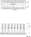
- FIG. 1 is a simplified flow chart of a method of manufacturing a semiconductor device according to an embodiment of the disclosure. As shown in FIG. 1 , the method includes the following steps, which is summarized here and explained further with reference to FIGS. 2A-4E .
- the substrate structure includes a conductive layer and a plurality of nanopillars spaced apart from each other over the conductive layer.
- Each of the nanopillars includes a first semiconductor layer and a second semiconductor layer on the first semiconductor layer.
- the first semiconductor layer and the second semiconductor layer are different in conductivity type.
- a PN junction is formed at the contact interface of the first semiconductor layer and the second semiconductor layer.
- Step 104 a graphene layer is formed on the plurality of nanopillars.
- the graphene layer is connected to each nanopillar.
- the semiconductor device obtained by the manufacturing method provided by the present disclosure can be used as a solar cell.
- the surface area of the nanopillars is significantly increased relative to the conventional solar cell, so that the absorption efficiency of the photon can be greatly improved, thereby improving the solar cell conversion efficiency.
- the graphene layer as the electrode of the solar cell can reduce the contact resistance between the electrode and the semiconductor, thereby improving the carrier mobility, thereby further improving the conversion efficiency of solar cells.
- FIGS. 2A-2C illustrate a method of manufacturing a semiconductor device according to one embodiment disclosed in different stages.
- the substrate structure includes a conductive layer 201 and a plurality of nanopillars 202 spaced apart from each other over conductive layer 201.
- the material of the conductive layer 201 may be an electrode of a material such as Al.
- Each nanopillar 202 includes a first semiconductor layer 212 and a second semiconductor layer 222.
- the first semiconductor layer 212 and the second semiconductor layer 222 may have different conductive types, so that the contact interface of the first semiconductor layer 212 with the second semiconductor layer 222 may form a PN junction 232.
- the semiconductor materials of the first material layer 212 and the second semiconductor layer 222 may be the same, thereby forming a homogeneous PN junction at the contact interface between the first semiconductor layer 212 and the second semiconductor layer 222.
- the semiconductor material of the first material layer 212 and the second semiconductor layer 222 may be different, so that they form a heterojunction at the junction interface of the first semiconductor layer 212 and the second semiconductor layer 222.
- the substrate structure may further include a substrate (not shown), the conductive layer 212 may be located on that substrate, which may be a support substrate.
- a graphene layer 203 is formed overlying the plurality of nanopillars 202.
- graphene layer 203 is in contact with all the nanopillars. In some cases, e.g., due to variations in the manufacturing process, some nanopillars may not be in contact with the graphene layer.
- a graphene layer may be formed on a metal substrate such as copper, platinum, tungsten, or nickel in advance; and then the graphene layer may be transferred over the plurality of nanopillars.
- the graphene layer can be formed using the following process.
- Methane, hydrogen, and argon gas are used as precursors, and a graphene layer is deposited on a copper substrate at a temperature of 700-1000 °C by chemical vapor deposition (CVD) or plasma enhanced chemical vapor deposition (PECVD). Then the graphene layer can be transferred to the nanopillars by wet transfer.
- CVD chemical vapor deposition
- PECVD plasma enhanced chemical vapor deposition
- the present disclosure is not limited thereto, and the transfer of graphene may also be carried out by other means.
- the semiconductor device in FIG. 2B includes a conductive layer 201 and a plurality of nanopillars 202 spaced apart from each other over conductive layer 201.
- Each nanopillar 202 includes a first semiconductor layer 212 and a second semiconductor layer 222.
- the first semiconductor layer 212 and the second semiconductor layer 222 have different conductive types.
- the contact interface of the first semiconductor layer 212 with the second semiconductor layer 222 may form a PN junction 232.
- the lateral dimensions of the nanopillars may be 5-5000 nm.
- a protective layer 204 may be formed on the graphene layer 203 in the semiconductor device shown in FIG. 2B .
- protective layer 204 may be a glass film; more preferably, the protection layer 204 may be a film of silica glass.
- FIGS. 3A-3C shows a method of manufacturing a semiconductor device according to an alternative embodiment of the present embodiment. Some of the components in FIGS. 3A-3C are similar to those in FIGS. 2A-2C , and references will be made to the corresponding parts in FIGS. 2A-2C .
- FIG. 3A shows a substrate structure.
- each of the nanopillars may also include an aluminum layer 242 on the second semiconductor layer 222.
- the substrate structure may further include a third semiconductor layer 205 on which the conductive layer 201 is disposed.
- the plurality of nanopillars 202 is disposed above the third semiconductor layer 205.
- the third semiconductor layer 205 and the first semiconductor layer 212 can have the same semiconductor material, e.g., silicon.
- the third semiconductor layer 205 and the first semiconductor layer 212 are shown as the same material. Similar to FIG. 2A , in FIG. 3A , the contact interface of the first semiconductor layer 212 with the second semiconductor layer 222 may form a PN junction 232.
- the graphene layer 203 is formed on the plurality of nanopillars 202.
- the graphene layer can be formed according to the manner described above.
- the semiconductor device includes a conductive layer 201, a third semiconductor layer 205 on conductive layer 201, and a plurality of spaced apart nanopillars 202 on the third semiconductor layer 205, and a graphene layer 203 on the plurality of nanopillars.
- the third semiconductor layer 205 and the first semiconductor layer 212 can be made of the same material.
- Each nanopillar 202 includes a first semiconductor layer 212, a second semiconductor layer 222 on the first semiconductor layer 212, and an aluminum layer 242 on the second semiconductor layer 222.
- the first semiconductor layer 212 and the second semiconductor layer 222 have different conductivity types, e.g., one is P-type and the other is N-type, or vice versa. As a result, a PN junction is formed at the contact interface 232 between the first semiconductor layer 212 and the second semiconductor layer 222.
- a protection layer 204 may be formed on the graphene layer 203.
- the protection layer can be, for example, a glass film.
- FIG. 2A and FIG. 3A can be formed in different ways.
- FIGS. 4A-4E describe a specific implementation of substrate structure.
- the initial substrate structure includes a conductive layer 201, a first semiconductor layer 212 on the conductive layer 201, a second semiconductor layer 222 on the first semiconductor layer 212, and an aluminum layer 242 on the second semiconductor layer 222.
- a PN junction is formed at a contact interface 232 between the first semiconductor layer 212 and the second semiconductor layer 222.
- Aluminum oxide layer 401 includes a plurality of nanopores 402.
- the plurality of nanopores 402 extends from the upper surface of the aluminum oxide layer 401 to a lower portion of aluminum layer 242. It should be understood that, as used herein, the terms “upper” and “lower” are only a relative concept, that is, relative to the lower portion of aluminum layer 242, the nanopores 402 are located at an upper portion of the aluminum layer 242.
- the lateral dimensions of the nanopores may be 5-5000 nm, e. g., 10 nm, 50 nm, 100 nm, 1000 nm, 3000 nm, and the like.
- the above-described anodic oxidation process may include the use of ammonium pentaborate and neutral solution of ammonium adipate and/or include phosphoric acid and oxalic acid electrolyte at a voltage of 0-100 V.
- the present disclosure is not limited thereto.
- One skilled in the art, in accordance with the teachings of the present disclosure can adjust the process conditions of the anodic oxidation process to obtain nanopores with different lateral dimensions.
- nanopore/pillar refers to the size and direction of the nanopore/pillar extending perpendicular to the direction of, for example, the nanopore extending vertically downward.
- the plurality of nanopores 402 are filled with a hard mask material 403.
- a hard mask material 403. titanium nitride may be deposited as a hard mask material 402 to fill the holes and cove the plurality of nanopores in aluminum oxide layer 401.
- CMP chemical mechanical polishing
- an etching process is carried out to sequentially etch the aluminum oxide layer 401, the lower portion of aluminum layer 242, the second semiconductor layer 222, and at least a portion of the first semiconductor layer 212.
- the material of the first semiconductor layer 212 and the second semiconductor layer 222 may include silicon.
- the second semiconductor layer 222 may be used as a plasma etching stop layer, and aluminum oxide layer 401 and the lower portion of aluminum layer 242 can be etched in a Cl (chlorine) containing plasma.
- BCl 3 can be used as a source gas for Cl containing plasma.
- a F (florine) containing plasma can be used to etch the second semiconductor layer 222 and at least a portion the first semiconductor layer 212.
- FIG. 4D only a portion of the first semiconductor layer 212 is removed.
- the first portion 212A that is not etched is shown in FIG. 3A as the third semiconductor layer 205.
- the remaining portion of the first semiconductor layer 212B and the second semiconductor layer 222 are part of the nanopillars in FIG. 3A .
- the etching of the first semiconductor layer 212 can be stopped on the conductive layer 201.
- the substrate structure shown in FIG. 3A is formed.
- the surface of the aluminum layer 242 in the nanopillars can be cleaned to remove the aluminum oxide.
- a weak alkaline cleaner may be used, e.g., sodium carbonate or triethanolamine, to clean the surface of aluminum layer 242 of the nanopillars.
- the substrate structure shown in FIG. 2A can be formed by removing the aluminum layer 242 from the second semiconductor layer 222.
Landscapes
- Chemical & Material Sciences (AREA)
- Engineering & Computer Science (AREA)
- Organic Chemistry (AREA)
- Materials Engineering (AREA)
- Nanotechnology (AREA)
- Inorganic Chemistry (AREA)
- Life Sciences & Earth Sciences (AREA)
- Sustainable Development (AREA)
- Sustainable Energy (AREA)
- Carbon And Carbon Compounds (AREA)
- Thin Film Transistor (AREA)
- Manufacturing & Machinery (AREA)
Abstract
Description
- This application claims priority to Chinese patent application No.
201610510623.2, filed on July 1, 2016 - The present invention relates to a semiconductor device and, more particularly, to a semiconductor device and a method for manufacturing a solar cell.
- With the growing global energy tensions, solar energy as a new energy has been vigorously developed. Solar cells are based on semiconductor materials, the use of photovoltaic materials to absorb light energy, and then photoelectric conversion, which will convert light energy. At present solar cells include monocrystalline silicon solar cells, polycrystalline silicon solar cells and amorphous silicon solar cells three categories, the industrialization of the conversion efficiency of solar cells is about 20%, respectively, 17%, 10%. Therefore, the conversion efficiency of existing solar cells is relatively low.
- It is an object of the present invention to propose a semiconductor device structure and method of manufacturing a semiconductor device by which the efficiency of solar cell conversion may be improved.
- The object is achieved by the features of the respective independent claims. Further embodiments are defined in the respective dependent claims.
- One aspect of the present invention provides a semiconductor device structure and another aspect provides a method of manufacturing a semiconductor device for improved performance of solar cells.
- According to a core aspect of the present invention, the device includes semiconductor nanopillars. The surface area of the nanopillars is significantly increased relative to the conventional planar solar cell, so that the absorption efficiency of the photon can be greatly improved, thereby improving the solar cell conversion efficiency. Further, a graphene layer is used as the electrode to connect the nanopillars of the solar cell and can reduce the contact resistance between the electrode and the semiconductor, thereby improving the carrier mobility, thereby further improving the conversion efficiency of solar cells.
- According to a first aspect of the present invention, a method of manufacturing a semiconductor device includes providing a substrate structure. The substrate structure includes a conductive layer and a plurality of nanopillars spaced apart from each other overlying the conductive layer. Each nanopillar includes a first semiconductor layer and a second semiconductor layer on the first semiconductor layer. The first semiconductor layer and the second semiconductor layer have different conductivity types. The method also includes forming a graphene layer overlying the plurality of nanopillars. The graphene layer is connected to each of the plurality of nanopillars. It is understood that due to manufacturing variability, in some cases, some of the nanopillars may not be connected to the graphene layer. In those cases, the plurality of nanopillars is understood to include those nanopillars that are connected to the graphene layer.
- Preferably, each of the nanopillars also includes an aluminum layer on the second semiconductor layer.
- Preferably, the substrate structure also includes a substrate, the conductive layer being disposed on the substrate.
- Preferably, the substrate structure also includes a third semiconductor layer disposed on the conductive layer, and the material of the third semiconductor layer is the same as the material of the first semiconductor layer. In this case, the plurality of nanopillars is positioned over the third semiconductor layer.
- Preferably, the step of providing a substrate structure includes: providing an initial substrate structure, the initial substrate structure comprising: a conductive layer; a first semiconductor layer overlying the conductive layer; a second semiconductor layer on said first semiconductor layer; and an aluminum layer on the second semiconductor layer; oxidizing an upper portion of the aluminum layer to form an aluminum oxide layer by an anodic oxidation process in which a plurality of nanopores are formed in the aluminum oxide layer, the nanopores extending from an upper surface of the aluminum oxide layer to a lower portion of the aluminum layer; filling a plurality of nanopores with a hard mask material; using the hard mask material in the nanopores as an etch mask to etching sequentially the aluminum oxide layer, the lower portion of the aluminum layer, the second semiconductor layer, and at least a portion of the first semiconductor layer; and removing the hard mask material, thereby forming the plurality of nanopillars.
- Preferably, the first semiconductor layer and the second semiconductor layer are silicon, and the method also includes using a Cl (chlorine) ion containing plasma to etch the alumina-containing layer and the aluminum layer with the second semiconductor layer as a plasma etching stop layer, and using a F (florine) ion containing plasma to etch the second semiconductor layer and at least a portion of the first semiconductor.
- Preferably, the anodic oxidation process is carried out with a voltage of 0-100 V utilizing an electrolyte comprising neutral ammonium pentaborate and ammonium adipate, or an electrolyte comprising phosphoric acid and oxalic acid electrolyte, or a combination of both electrolytes.
- Preferably, the method further includes after removal of the hard mask, cleaning the surface of the aluminum layer in the nanopillars.
- Preferably, the transverse dimension of the nanopores is 5-5000 nm.
- Preferably, the transverse dimension of the nanopillars is 5-5000 nm.
- Preferably, the formation of the graphene layer includes forming a graphene layer on a metal substrate, and transferring the graphene layer over the plurality of nanopillars.
- Preferably, the method also includes forming a protective layer on the graphene layer.
- Preferably, the first semiconductor layer and the second semiconductor layer are formed by the same material.
- Preferably, the first semiconductor layer and the second semiconductor layer are formed by different material.
- According to a second aspect of the present invention, a semiconductor device includes a conductive layer and a plurality of nanopillars spaced apart from each other overlying the conductive layer. Each nanopillar includes a first semiconductor layer and a second semiconductor layer on the first semiconductor layer. The first semiconductor layer is different in conductivity type from the second semiconductor layer. The semiconductor device also has a graphene layer overlying the plurality of nanopillars, the graphene layer being connected to each of the plurality of nanopillars.
- Preferably, each of the nanopillars further includes an aluminum layer on the second semiconductor layer.
- Preferably, the device also includes a third semiconductor layer on the conductive layer, and the material of the third semiconductor layer and the material of the first semiconductor layer are the same. In this case, the plurality of nanopillars are located over the third semiconductor layer.
- Preferably, the device also includes a substrate, and the conductive layer is disposed on the substrate.
- Preferably, the device also includes a protective layer on the graphene layer.
- Preferably, the transverse dimension of the nanopillars is 5-5000 nm.
- Preferably, the material of the first semiconductor layer is the same as the material of the second semiconductor layer.
- Preferably, the material of the first semiconductor layer is different than the material of the second semiconductor layer.
- A semiconductor device according to the second aspect of the present invention may be obtained by a method according to the first aspect of the present invention.
- A further understanding of the nature and advantages of the present invention may be realized by reference to the remaining portions of the specification and the drawings.
-
-
FIG. 1 is a simplified flow chart of a method of manufacturing a semiconductor device according to an embodiment of the present invention; -
FIG. 2A shows a cross sectional view of a substrate structure according to an embodiment of the present invention; -
FIG. 2B shows a cross sectional view of the graphene layer formed in a plurality of nanopillars according to an embodiment of the present invention; -
FIG. 2C shows a cross sectional view of forming a protective layer on the graphene layer in accordance with one embodiment of the present invention; -
FIG. 3A illustrates a cross sectional view of an example of the structure of the substrate according to another embodiment of the present invention; -
FIG. 3B illustrates a cross sectional view of a graphene layer formed on a plurality of nanopillars according to another embodiment of the present invention; -
FIG. 3C illustrates a cross sectional view of forming a protection layer on the graphene layer according to another embodiment of the present invention; -
FIG. 4A shows a cross cross-sectional view of the formation of a substrate structure according to another embodiment of the present invention; -
FIG. 4B shows a cross cross-sectional view of the formation of a substrate structure according to another embodiment of the present invention; -
FIG. 4C shows a cross cross-sectional view of a stage of forming a substrate structure according to another embodiment of the present invention; -
FIG. 4D shows a cross cross-sectional view of a stage of formation of a substrate structure according to another embodiment of the present invention; and -
FIG. 4E shows a cross cross-sectional view of a stage of forming a substrate structure of the present embodiment of the present invention. - The various exemplary embodiments of the present invention will now be described in detail with reference to the accompanying drawings. It should be understood that the relative arrangements, numerical expressions, and numerical values of the components and steps set forth in these embodiments should not be construed as limiting the invention unless otherwise specifically stated.
- In addition, it should be understood that the dimensions of the various components shown in the figures are not necessarily drawn in an actual scale relationship for ease of description, such as the thickness or width of certain layers may be exaggerated relative to other layers.
- The following description of exemplary embodiments is illustrative only and is not to be taken as a limitation on the invention, its application or use in any sense. Techniques, methods, and apparatus known to those of ordinary skill in the relevant art may not be discussed in detail, but such techniques, methods, and apparatuses should be considered as part of this description insofar as they apply to such techniques, methods, and apparatuses. It should be noted that like reference numerals and letters designate like items in the following drawings, and therefore, once an item is defined or illustrated in one of the drawings, the detailed description is not repeated.
-
FIG. 1 is a simplified flow chart of a method of manufacturing a semiconductor device according to an embodiment of the disclosure. As shown inFIG. 1 , the method includes the following steps, which is summarized here and explained further with reference toFIGS. 2A-4E . -
Step 102, a substrate structure is provided. The substrate structure includes a conductive layer and a plurality of nanopillars spaced apart from each other over the conductive layer. Each of the nanopillars includes a first semiconductor layer and a second semiconductor layer on the first semiconductor layer. The first semiconductor layer and the second semiconductor layer are different in conductivity type. A PN junction is formed at the contact interface of the first semiconductor layer and the second semiconductor layer. -
Step 104, a graphene layer is formed on the plurality of nanopillars. The graphene layer is connected to each nanopillar. - The semiconductor device obtained by the manufacturing method provided by the present disclosure can be used as a solar cell. On the one hand, the surface area of the nanopillars is significantly increased relative to the conventional solar cell, so that the absorption efficiency of the photon can be greatly improved, thereby improving the solar cell conversion efficiency. On the other hand, the graphene layer as the electrode of the solar cell can reduce the contact resistance between the electrode and the semiconductor, thereby improving the carrier mobility, thereby further improving the conversion efficiency of solar cells.
-
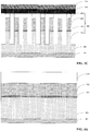
FIGS. 2A-2C illustrate a method of manufacturing a semiconductor device according to one embodiment disclosed in different stages. - First, as shown in
FIG. 2A , a substrate structure is provided. The substrate structure includes aconductive layer 201 and a plurality ofnanopillars 202 spaced apart from each other overconductive layer 201. The material of theconductive layer 201 may be an electrode of a material such as Al. Eachnanopillar 202 includes afirst semiconductor layer 212 and asecond semiconductor layer 222. Here, thefirst semiconductor layer 212 and thesecond semiconductor layer 222 may have different conductive types, so that the contact interface of thefirst semiconductor layer 212 with thesecond semiconductor layer 222 may form aPN junction 232. In one embodiment, the semiconductor materials of thefirst material layer 212 and thesecond semiconductor layer 222 may be the same, thereby forming a homogeneous PN junction at the contact interface between thefirst semiconductor layer 212 and thesecond semiconductor layer 222. In another embodiment, the semiconductor material of thefirst material layer 212 and thesecond semiconductor layer 222 may be different, so that they form a heterojunction at the junction interface of thefirst semiconductor layer 212 and thesecond semiconductor layer 222. Further, the substrate structure may further include a substrate (not shown), theconductive layer 212 may be located on that substrate, which may be a support substrate. - Thereafter, as shown in
FIG. 2B , agraphene layer 203 is formed overlying the plurality ofnanopillars 202. In some embodiments,graphene layer 203 is in contact with all the nanopillars. In some cases, e.g., due to variations in the manufacturing process, some nanopillars may not be in contact with the graphene layer. In one embodiment, a graphene layer may be formed on a metal substrate such as copper, platinum, tungsten, or nickel in advance; and then the graphene layer may be transferred over the plurality of nanopillars. For example, the graphene layer can be formed using the following process. Methane, hydrogen, and argon gas are used as precursors, and a graphene layer is deposited on a copper substrate at a temperature of 700-1000 °C by chemical vapor deposition (CVD) or plasma enhanced chemical vapor deposition (PECVD). Then the graphene layer can be transferred to the nanopillars by wet transfer. However, the present disclosure is not limited thereto, and the transfer of graphene may also be carried out by other means. - A description of the device structure of the semiconductor device formed above is presented below with reference to
FIG. 2B . The semiconductor device inFIG. 2B includes aconductive layer 201 and a plurality ofnanopillars 202 spaced apart from each other overconductive layer 201. Eachnanopillar 202 includes afirst semiconductor layer 212 and asecond semiconductor layer 222. Thefirst semiconductor layer 212 and thesecond semiconductor layer 222 have different conductive types. The contact interface of thefirst semiconductor layer 212 with thesecond semiconductor layer 222 may form aPN junction 232. In one embodiment, the lateral dimensions of the nanopillars may be 5-5000 nm. - Thereafter, as shown in
FIG. 2C , aprotective layer 204 may be formed on thegraphene layer 203 in the semiconductor device shown inFIG. 2B . Preferably,protective layer 204 may be a glass film; more preferably, theprotection layer 204 may be a film of silica glass. -
FIGS. 3A-3C shows a method of manufacturing a semiconductor device according to an alternative embodiment of the present embodiment. Some of the components inFIGS. 3A-3C are similar to those inFIGS. 2A-2C , and references will be made to the corresponding parts inFIGS. 2A-2C . - First,
FIG. 3A shows a substrate structure. Compared with the substrate structure shown inFIG. 2A , in the substrate structure shown inFIG. 3A , each of the nanopillars may also include analuminum layer 242 on thesecond semiconductor layer 222. Further, the substrate structure may further include athird semiconductor layer 205 on which theconductive layer 201 is disposed. In this case, the plurality ofnanopillars 202 is disposed above thethird semiconductor layer 205. Here, thethird semiconductor layer 205 and thefirst semiconductor layer 212 can have the same semiconductor material, e.g., silicon. InFIG. 3A , thethird semiconductor layer 205 and thefirst semiconductor layer 212 are shown as the same material. Similar toFIG. 2A , inFIG. 3A , the contact interface of thefirst semiconductor layer 212 with thesecond semiconductor layer 222 may form aPN junction 232. - Then, as shown in
FIG. 3B , thegraphene layer 203 is formed on the plurality ofnanopillars 202. The graphene layer can be formed according to the manner described above. As shown inFIG. 3B , the semiconductor device includes aconductive layer 201, athird semiconductor layer 205 onconductive layer 201, and a plurality of spaced apart nanopillars 202 on thethird semiconductor layer 205, and agraphene layer 203 on the plurality of nanopillars. Thethird semiconductor layer 205 and thefirst semiconductor layer 212 can be made of the same material. Eachnanopillar 202 includes afirst semiconductor layer 212, asecond semiconductor layer 222 on thefirst semiconductor layer 212, and analuminum layer 242 on thesecond semiconductor layer 222. Thefirst semiconductor layer 212 and thesecond semiconductor layer 222 have different conductivity types, e.g., one is P-type and the other is N-type, or vice versa. As a result, a PN junction is formed at thecontact interface 232 between thefirst semiconductor layer 212 and thesecond semiconductor layer 222. - Thereafter, as shown in
Fig. 3C , aprotection layer 204 may be formed on thegraphene layer 203. The protection layer can be, for example, a glass film. - The substrate structures in
FIG. 2A andFIG. 3A , and can be formed in different ways.FIGS. 4A-4E , describe a specific implementation of substrate structure. - First, as shown in
FIG. 4A , an initial substrate structure is provided. The initial substrate structure includes aconductive layer 201, afirst semiconductor layer 212 on theconductive layer 201, asecond semiconductor layer 222 on thefirst semiconductor layer 212, and analuminum layer 242 on thesecond semiconductor layer 222. A PN junction is formed at acontact interface 232 between thefirst semiconductor layer 212 and thesecond semiconductor layer 222. - Then, as shown in
Fig. 4B , an upper portion ofaluminum layer 242 is oxidized to form analuminum oxide layer 401 using an anodizing process.Aluminum oxide layer 401 includes a plurality ofnanopores 402. The plurality ofnanopores 402 extends from the upper surface of thealuminum oxide layer 401 to a lower portion ofaluminum layer 242. It should be understood that, as used herein, the terms "upper" and "lower" are only a relative concept, that is, relative to the lower portion ofaluminum layer 242, thenanopores 402 are located at an upper portion of thealuminum layer 242. - In one embodiment, the lateral dimensions of the nanopores (e.g., diameter) may be 5-5000 nm, e. g., 10 nm, 50 nm, 100 nm, 1000 nm, 3000 nm, and the like. In one embodiment, the above-described anodic oxidation process may include the use of ammonium pentaborate and neutral solution of ammonium adipate and/or include phosphoric acid and oxalic acid electrolyte at a voltage of 0-100 V. However, the present disclosure is not limited thereto. One skilled in the art, in accordance with the teachings of the present disclosure, can adjust the process conditions of the anodic oxidation process to obtain nanopores with different lateral dimensions.
- It should be noted that the "horizontal dimension" herein nanopore/pillar refers to the size and direction of the nanopore/pillar extending perpendicular to the direction of, for example, the nanopore extending vertically downward.
- Next, as shown in
FIG. 4C , the plurality ofnanopores 402 are filled with ahard mask material 403. For example, titanium nitride may be deposited as ahard mask material 402 to fill the holes and cove the plurality of nanopores inaluminum oxide layer 401. After the hard mask material is planarized, e. g., using chemical mechanical polishing (CMP), the surface of thealumina layer 401 is substantially flush with the surface ofhard mask material 403. - Next, as shown in
FIG. 4D and 4E , withhard mask 403 as an etching mask, an etching process is carried out to sequentially etch thealuminum oxide layer 401, the lower portion ofaluminum layer 242, thesecond semiconductor layer 222, and at least a portion of thefirst semiconductor layer 212. In one embodiment, the material of thefirst semiconductor layer 212 and thesecond semiconductor layer 222 may include silicon. In an embodiment, thesecond semiconductor layer 222 may be used as a plasma etching stop layer, andaluminum oxide layer 401 and the lower portion ofaluminum layer 242 can be etched in a Cl (chlorine) containing plasma. For example, BCl3 can be used as a source gas for Cl containing plasma. In some embodiments, a F (florine) containing plasma can be used to etch thesecond semiconductor layer 222 and at least a portion thefirst semiconductor layer 212. - In one implementation, shown in
FIG. 4D , only a portion of thefirst semiconductor layer 212 is removed. Thefirst portion 212A that is not etched is shown inFIG. 3A as thethird semiconductor layer 205. The remaining portion of thefirst semiconductor layer 212B and thesecond semiconductor layer 222 are part of the nanopillars inFIG. 3A . - In another implementation, as shown in
FIG. 4E , the etching of thefirst semiconductor layer 212 can be stopped on theconductive layer 201. - After removal of the
hard mask 403, the substrate structure shown inFIG. 3A is formed. After removing thehard mask 403, the surface of thealuminum layer 242 in the nanopillars can be cleaned to remove the aluminum oxide. In one embodiment, a weak alkaline cleaner may be used, e.g., sodium carbonate or triethanolamine, to clean the surface ofaluminum layer 242 of the nanopillars. - Further, the substrate structure shown in
FIG. 2A can be formed by removing thealuminum layer 242 from thesecond semiconductor layer 222.
Claims (14)
- A method of manufacturing a semiconductor device, comprising:providing a substrate structure, the substrate structure comprising:a conductive layer; anda plurality of nanopillars spaced apart from each other overlying the conductive layer, each nanopillar comprising a first semiconductor layer and a second semiconductor layer on the first semiconductor layer, the first semiconductor layer and the second semiconductor layer having different conductivity types; andforming a graphene layer overlying the plurality of nanopillars, the graphene layer being connected to each of the plurality of nanopillars.
- The method according to claim 1, wherein at least one of:each of the nanopillars further comprises an aluminum layer on the second semiconductor layer;said substrate structure further comprises a substrate, the conductive layer being disposed on the substrate; andsaid substrate structure further comprises a third semiconductor layer disposed on the conductive layer, the material of the third semiconductor layer is the same as the material of the first semiconductor layer, the plurality of nanopillars being positioned over the third semiconductor layer.
- The method as claimed in claim 2, wherein said step of providing a substrate structure comprises:providing an initial substrate structure, the initial substrate structure comprising:a conductive layer;a first semiconductor layer overlying the conductive layer;a second semiconductor layer on said first semiconductor layer; andan aluminum layer on the second semiconductor layer;oxidizing an upper portion of the aluminum layer to form an aluminum oxide layer by an anodic oxidation process in which a plurality of nanopores are formed in the aluminum oxide layer, the nanopores extending from an upper surface of the aluminum oxide layer to a lower portion of the aluminum layer;filling a plurality of nanopores with a hard mask material;using the hard mask material in the nanopores as an etch mask to etching sequentially the aluminum oxide layer, the lower portion of the aluminum layer, the second semiconductor layer, and at least a portion of the first semiconductor layer; andremoving the hard mask material, thereby forming the plurality of nanopillars.
- The method according to claim 3, wherein the first semiconductor layer and the second semiconductor layer comprise silicon; and
wherein the method further comprising:using a Cl (chlorine) ion containing plasma to etch the alumina-containing layer and the aluminum layer with the second semiconductor layer as a plasma etching stop layer;using a F (florine) ion containing plasma to etch the second semiconductor layer and at least a portion of the first semiconductor. - The method according to claim 3, wherein the anodic oxidation process is carried out with a voltage of 0-100 V utilizing an electrolyte comprising neutral ammonium pentaborate and ammonium adipate, or an electrolyte comprising phosphoric acid and oxalic acid electrolyte, or a combination of both electrolytes.
- The method according to claim 3, further comprising:after removal of the hard mask, cleaning the surface of the aluminum layer in the nanopillars.
- The method according to claim 3, wherein:the transverse dimension of the nanopores is 5-5000 nm; and/orthe transverse dimension of the nanopillars 5-5000 nm.
- The method according to anyone of the claims 1-7, wherein
forming the graphene layer comprises: forming a graphene layer on a metal substrate;
and transferring the graphene layer over the plurality of nanopillars; and/or
the method further comprises: forming a protective layer on the graphene layer. - The method according to anyone of the claims 1-8, wherein
the first semiconductor layer and the second semiconductor layer are formed by the same material; and/or
the first semiconductor layer and the second semiconductor layer are formed by different material. - A semiconductor device, comprising:a conductive layer;a plurality of nanopillars spaced apart from each other overlying the conductive layer, each nanopillar comprising a first semiconductor layer and a second semiconductor layer on the first semiconductor layer, the first semiconductor layer being different in conductivity type from the second semiconductor layer; anda graphene layer overlying the plurality of nanopillars, the graphene layer being connected to each of the plurality of nanopillars.
- The device according to claim 10, wherein
each of the nanopillars further includes an aluminum layer on the second semiconductor layer. - The device according to claim 10 or 11, wherein the transverse dimension of the nanopillars is 5-5000 nm.
- The device according to anyone of the claims 10-12, further comprising at least one of:a third semiconductor layer on the conductive layer, the material of the third semiconductor layer and the material of the first semiconductor layer are the same, wherein the plurality of nanopillars are located over the third semiconductor layer;a substrate, the conductive layer being disposed on the substrate;a protective layer on the graphene layer.
- The device according to anyone of the claims 10-12, wherein
the material of the first semiconductor layer is the same as the material of the second semiconductor layer; or, alternatively,
the material of the first semiconductor layer is different than the material of the second semiconductor layer.
Applications Claiming Priority (1)
| Application Number | Priority Date | Filing Date | Title |
|---|---|---|---|
| CN201610510623.2A CN107564980B (en) | 2016-07-01 | 2016-07-01 | Semiconductor device and method for manufacturing the same |
Publications (1)
| Publication Number | Publication Date |
|---|---|
| EP3264474A1 true EP3264474A1 (en) | 2018-01-03 |
Family
ID=59253371
Family Applications (1)
| Application Number | Title | Priority Date | Filing Date |
|---|---|---|---|
| EP17178367.3A Withdrawn EP3264474A1 (en) | 2016-07-01 | 2017-06-28 | Method for fabricating nanopillar solar cell using graphene |
Country Status (3)
| Country | Link |
|---|---|
| US (2) | US11139405B2 (en) |
| EP (1) | EP3264474A1 (en) |
| CN (1) | CN107564980B (en) |
Families Citing this family (3)
| Publication number | Priority date | Publication date | Assignee | Title |
|---|---|---|---|---|
| US11239415B2 (en) * | 2019-04-18 | 2022-02-01 | Nanya Technology Corporation | Memory device and fabrication method thereof |
| CN112186055B (en) * | 2020-09-29 | 2022-01-07 | 复旦大学 | A combined solar energy three-dimensional integrated system and preparation method thereof |
| CN113948546A (en) * | 2021-09-17 | 2022-01-18 | 国家电投集团科学技术研究院有限公司 | Laminated battery and preparation method thereof |
Citations (8)
| Publication number | Priority date | Publication date | Assignee | Title |
|---|---|---|---|---|
| US20040157354A1 (en) * | 2002-12-13 | 2004-08-12 | Akira Kuriyama | Semiconductor device and method of manufacturing the same |
| US20060207647A1 (en) * | 2005-03-16 | 2006-09-21 | General Electric Company | High efficiency inorganic nanorod-enhanced photovoltaic devices |
| US20110308564A1 (en) * | 2005-08-24 | 2011-12-22 | The Trustees Of Boston College | Apparatus and Methods for Solar Energy Conversion Using Nanoscale Cometal Structures |
| US20130019924A1 (en) * | 2009-11-25 | 2013-01-24 | The Trustees Of Boston College | Nanoscopically Thin Photovoltaic Junction Solar Cells |
| CN103219413A (en) * | 2013-04-10 | 2013-07-24 | 中国科学院微电子研究所 | A kind of graphene radial heterojunction solar cell and preparation method thereof |
| US20140096816A1 (en) * | 2010-12-22 | 2014-04-10 | Harry A. Atwater | Heterojunction microwire array semiconductor devices |
| US20140326305A1 (en) * | 2011-08-19 | 2014-11-06 | Postech Academy-Industry Foundation | Solar cell and method for manufacturing same |
| US20160126416A1 (en) * | 2013-05-14 | 2016-05-05 | Commissariat Á L'energie Atomique Et Aux Énergies Alternatives | Optoelectronic device and method for manufacturing same |
Family Cites Families (10)
| Publication number | Priority date | Publication date | Assignee | Title |
|---|---|---|---|---|
| US5581091A (en) * | 1994-12-01 | 1996-12-03 | Moskovits; Martin | Nanoelectric devices |
| JP5667748B2 (en) * | 2009-03-18 | 2015-02-12 | 株式会社東芝 | Light transmissive solar cell and method for manufacturing the same |
| US10164135B2 (en) * | 2009-08-07 | 2018-12-25 | Guardian Glass, LLC | Electronic device including graphene-based layer(s), and/or method or making the same |
| US8513722B2 (en) * | 2010-03-02 | 2013-08-20 | Micron Technology, Inc. | Floating body cell structures, devices including same, and methods for forming same |
| JP2012074569A (en) * | 2010-09-29 | 2012-04-12 | Jx Nippon Oil & Energy Corp | Photoelectric conversion element |
| WO2013062727A1 (en) * | 2011-10-24 | 2013-05-02 | Applied Materials, Inc. | Method and apparatus of removing a passivation film and improving contact resistance in rear point contact solar cells |
| US20140251411A1 (en) * | 2013-03-05 | 2014-09-11 | Qualcomm Mems Technologies, Inc. | Large area photovoltaic energy-collecting window/skylight |
| US9390923B2 (en) * | 2014-07-03 | 2016-07-12 | Applied Materials, Inc. | Methods of removing residual polymers formed during a boron-doped amorphous carbon layer etch process |
| US9147875B1 (en) * | 2014-09-10 | 2015-09-29 | Cellink Corporation | Interconnect for battery packs |
| JP6030176B2 (en) * | 2015-03-19 | 2016-11-24 | 株式会社東芝 | Photoelectric conversion element and manufacturing method thereof |
-
2016
- 2016-07-01 CN CN201610510623.2A patent/CN107564980B/en active Active
-
2017
- 2017-04-03 US US15/477,798 patent/US11139405B2/en active Active
- 2017-06-28 EP EP17178367.3A patent/EP3264474A1/en not_active Withdrawn
-
2021
- 2021-08-25 US US17/445,879 patent/US20210391483A1/en not_active Abandoned
Patent Citations (8)
| Publication number | Priority date | Publication date | Assignee | Title |
|---|---|---|---|---|
| US20040157354A1 (en) * | 2002-12-13 | 2004-08-12 | Akira Kuriyama | Semiconductor device and method of manufacturing the same |
| US20060207647A1 (en) * | 2005-03-16 | 2006-09-21 | General Electric Company | High efficiency inorganic nanorod-enhanced photovoltaic devices |
| US20110308564A1 (en) * | 2005-08-24 | 2011-12-22 | The Trustees Of Boston College | Apparatus and Methods for Solar Energy Conversion Using Nanoscale Cometal Structures |
| US20130019924A1 (en) * | 2009-11-25 | 2013-01-24 | The Trustees Of Boston College | Nanoscopically Thin Photovoltaic Junction Solar Cells |
| US20140096816A1 (en) * | 2010-12-22 | 2014-04-10 | Harry A. Atwater | Heterojunction microwire array semiconductor devices |
| US20140326305A1 (en) * | 2011-08-19 | 2014-11-06 | Postech Academy-Industry Foundation | Solar cell and method for manufacturing same |
| CN103219413A (en) * | 2013-04-10 | 2013-07-24 | 中国科学院微电子研究所 | A kind of graphene radial heterojunction solar cell and preparation method thereof |
| US20160126416A1 (en) * | 2013-05-14 | 2016-05-05 | Commissariat Á L'energie Atomique Et Aux Énergies Alternatives | Optoelectronic device and method for manufacturing same |
Also Published As
| Publication number | Publication date |
|---|---|
| CN107564980A (en) | 2018-01-09 |
| US20180006169A1 (en) | 2018-01-04 |
| US11139405B2 (en) | 2021-10-05 |
| US20210391483A1 (en) | 2021-12-16 |
| CN107564980B (en) | 2020-03-31 |
Similar Documents
| Publication | Publication Date | Title |
|---|---|---|
| US10957809B2 (en) | Solar cell having an emitter region with wide bandgap semiconductor material | |
| CN102160192B (en) | Method for fabricating solar cell using direct-pattern pin-hole-free masking layer | |
| US20210391483A1 (en) | Nanopillar solar cell using graphene | |
| TWI565092B (en) | Porous semiconductor photovoltaic cells designed with contact terminals/electrolytic etching modules and related production lines | |
| TWI665807B (en) | Solar cells with tunnel dielectrics | |
| US7670638B2 (en) | Protection layer for fabricating a solar cell | |
| US20100108130A1 (en) | Thin Interdigitated backside contact solar cell and manufacturing process thereof | |
| CN102165605A (en) | Quantum dot photovoltaic device and manufacturing method thereof | |
| CN102369601A (en) | Solar cell | |
| CN106062975B (en) | The manufacture method and solar cell of solar cell | |
| CN110168742A (en) | Method for fabricating photovoltaic cells with backside polysilicon passivated contacts | |
| TW201520383A (en) | Electropolishing and porosification | |
| CN101969082B (en) | Process for manufacturing solar cell by twice screen printing and grooving | |
| TW202017180A (en) | Integrated circuit device | |
| TW201705505A (en) | Passivation layer of solar cell | |
| US20130164902A1 (en) | Methods Of Forming Capacitors | |
| CN103346210A (en) | Solar cell and manufacturing method thereof | |
| CN104471663A (en) | Energy storage devices with at least one porous polycrystalline substrate | |
| KR20120036948A (en) | Photoelectric conversion device | |
| CN104555897A (en) | Method for electrochemically producing at least one porous region of a micro- and/or nanoelectronic structure | |
| TW201431108A (en) | A process of manufacturing an interdigitated back-contact solar cell | |
| CN105810734B (en) | Semiconductor device and its manufacturing method | |
| CN114068672B (en) | Semiconductor element and method for manufacturing the same | |
| CN103515458A (en) | Method and structure for integration of a titania layer in an anti-reflective coating | |
| CN104425654A (en) | Etching method |
Legal Events
| Date | Code | Title | Description |
|---|---|---|---|
| PUAI | Public reference made under article 153(3) epc to a published international application that has entered the european phase |
Free format text: ORIGINAL CODE: 0009012 |
|
| STAA | Information on the status of an ep patent application or granted ep patent |
Free format text: STATUS: THE APPLICATION HAS BEEN PUBLISHED |
|
| AK | Designated contracting states |
Kind code of ref document: A1 Designated state(s): AL AT BE BG CH CY CZ DE DK EE ES FI FR GB GR HR HU IE IS IT LI LT LU LV MC MK MT NL NO PL PT RO RS SE SI SK SM TR |
|
| AX | Request for extension of the european patent |
Extension state: BA ME |
|
| STAA | Information on the status of an ep patent application or granted ep patent |
Free format text: STATUS: REQUEST FOR EXAMINATION WAS MADE |
|
| 17P | Request for examination filed |
Effective date: 20180622 |
|
| RBV | Designated contracting states (corrected) |
Designated state(s): AL AT BE BG CH CY CZ DE DK EE ES FI FR GB GR HR HU IE IS IT LI LT LU LV MC MK MT NL NO PL PT RO RS SE SI SK SM TR |
|
| RAP1 | Party data changed (applicant data changed or rights of an application transferred) |
Owner name: SEMICONDUCTOR MANUFACTURING INTERNATIONAL (BEIJING Owner name: SEMICONDUCTOR MANUFACTURING INTERNATIONAL (SHANGHA |
|
| GRAP | Despatch of communication of intention to grant a patent |
Free format text: ORIGINAL CODE: EPIDOSNIGR1 |
|
| STAA | Information on the status of an ep patent application or granted ep patent |
Free format text: STATUS: GRANT OF PATENT IS INTENDED |
|
| RIC1 | Information provided on ipc code assigned before grant |
Ipc: H01L 31/0352 20060101AFI20181114BHEP Ipc: H01L 31/0224 20060101ALI20181114BHEP |
|
| INTG | Intention to grant announced |
Effective date: 20181213 |
|
| STAA | Information on the status of an ep patent application or granted ep patent |
Free format text: STATUS: THE APPLICATION IS DEEMED TO BE WITHDRAWN |
|
| 18D | Application deemed to be withdrawn |
Effective date: 20190424 |