EP3264468A1 - Coplanar type oxide thin film transistor, method of manufacturing the same, and display panel and display device using the same - Google Patents
Coplanar type oxide thin film transistor, method of manufacturing the same, and display panel and display device using the same Download PDFInfo
- Publication number
- EP3264468A1 EP3264468A1 EP16207507.1A EP16207507A EP3264468A1 EP 3264468 A1 EP3264468 A1 EP 3264468A1 EP 16207507 A EP16207507 A EP 16207507A EP 3264468 A1 EP3264468 A1 EP 3264468A1
- Authority
- EP
- European Patent Office
- Prior art keywords
- gate
- conductor
- layer
- contact hole
- insulation layer
- Prior art date
- Legal status (The legal status is an assumption and is not a legal conclusion. Google has not performed a legal analysis and makes no representation as to the accuracy of the status listed.)
- Ceased
Links
Images



Classifications
-
- H—ELECTRICITY
- H10—SEMICONDUCTOR DEVICES; ELECTRIC SOLID-STATE DEVICES NOT OTHERWISE PROVIDED FOR
- H10D—INORGANIC ELECTRIC SEMICONDUCTOR DEVICES
- H10D86/00—Integrated devices formed in or on insulating or conducting substrates, e.g. formed in silicon-on-insulator [SOI] substrates or on stainless steel or glass substrates
- H10D86/40—Integrated devices formed in or on insulating or conducting substrates, e.g. formed in silicon-on-insulator [SOI] substrates or on stainless steel or glass substrates characterised by multiple TFTs
- H10D86/60—Integrated devices formed in or on insulating or conducting substrates, e.g. formed in silicon-on-insulator [SOI] substrates or on stainless steel or glass substrates characterised by multiple TFTs wherein the TFTs are in active matrices
-
- H—ELECTRICITY
- H10—SEMICONDUCTOR DEVICES; ELECTRIC SOLID-STATE DEVICES NOT OTHERWISE PROVIDED FOR
- H10D—INORGANIC ELECTRIC SEMICONDUCTOR DEVICES
- H10D30/00—Field-effect transistors [FET]
- H10D30/60—Insulated-gate field-effect transistors [IGFET]
- H10D30/67—Thin-film transistors [TFT]
- H10D30/674—Thin-film transistors [TFT] characterised by the active materials
- H10D30/6755—Oxide semiconductors, e.g. zinc oxide, copper aluminium oxide or cadmium stannate
-
- G—PHYSICS
- G02—OPTICS
- G02F—OPTICAL DEVICES OR ARRANGEMENTS FOR THE CONTROL OF LIGHT BY MODIFICATION OF THE OPTICAL PROPERTIES OF THE MEDIA OF THE ELEMENTS INVOLVED THEREIN; NON-LINEAR OPTICS; FREQUENCY-CHANGING OF LIGHT; OPTICAL LOGIC ELEMENTS; OPTICAL ANALOGUE/DIGITAL CONVERTERS
- G02F1/00—Devices or arrangements for the control of the intensity, colour, phase, polarisation or direction of light arriving from an independent light source, e.g. switching, gating or modulating; Non-linear optics
- G02F1/01—Devices or arrangements for the control of the intensity, colour, phase, polarisation or direction of light arriving from an independent light source, e.g. switching, gating or modulating; Non-linear optics for the control of the intensity, phase, polarisation or colour
- G02F1/13—Devices or arrangements for the control of the intensity, colour, phase, polarisation or direction of light arriving from an independent light source, e.g. switching, gating or modulating; Non-linear optics for the control of the intensity, phase, polarisation or colour based on liquid crystals, e.g. single liquid crystal display cells
- G02F1/133—Constructional arrangements; Operation of liquid crystal cells; Circuit arrangements
- G02F1/136—Liquid crystal cells structurally associated with a semi-conducting layer or substrate, e.g. cells forming part of an integrated circuit
- G02F1/1362—Active matrix addressed cells
- G02F1/136209—Light shielding layers, e.g. black matrix, incorporated in the active matrix substrate, e.g. structurally associated with the switching element
-
- G—PHYSICS
- G02—OPTICS
- G02F—OPTICAL DEVICES OR ARRANGEMENTS FOR THE CONTROL OF LIGHT BY MODIFICATION OF THE OPTICAL PROPERTIES OF THE MEDIA OF THE ELEMENTS INVOLVED THEREIN; NON-LINEAR OPTICS; FREQUENCY-CHANGING OF LIGHT; OPTICAL LOGIC ELEMENTS; OPTICAL ANALOGUE/DIGITAL CONVERTERS
- G02F1/00—Devices or arrangements for the control of the intensity, colour, phase, polarisation or direction of light arriving from an independent light source, e.g. switching, gating or modulating; Non-linear optics
- G02F1/01—Devices or arrangements for the control of the intensity, colour, phase, polarisation or direction of light arriving from an independent light source, e.g. switching, gating or modulating; Non-linear optics for the control of the intensity, phase, polarisation or colour
- G02F1/13—Devices or arrangements for the control of the intensity, colour, phase, polarisation or direction of light arriving from an independent light source, e.g. switching, gating or modulating; Non-linear optics for the control of the intensity, phase, polarisation or colour based on liquid crystals, e.g. single liquid crystal display cells
- G02F1/133—Constructional arrangements; Operation of liquid crystal cells; Circuit arrangements
- G02F1/136—Liquid crystal cells structurally associated with a semi-conducting layer or substrate, e.g. cells forming part of an integrated circuit
- G02F1/1362—Active matrix addressed cells
- G02F1/136286—Wiring, e.g. gate line, drain line
-
- G—PHYSICS
- G02—OPTICS
- G02F—OPTICAL DEVICES OR ARRANGEMENTS FOR THE CONTROL OF LIGHT BY MODIFICATION OF THE OPTICAL PROPERTIES OF THE MEDIA OF THE ELEMENTS INVOLVED THEREIN; NON-LINEAR OPTICS; FREQUENCY-CHANGING OF LIGHT; OPTICAL LOGIC ELEMENTS; OPTICAL ANALOGUE/DIGITAL CONVERTERS
- G02F1/00—Devices or arrangements for the control of the intensity, colour, phase, polarisation or direction of light arriving from an independent light source, e.g. switching, gating or modulating; Non-linear optics
- G02F1/01—Devices or arrangements for the control of the intensity, colour, phase, polarisation or direction of light arriving from an independent light source, e.g. switching, gating or modulating; Non-linear optics for the control of the intensity, phase, polarisation or colour
- G02F1/13—Devices or arrangements for the control of the intensity, colour, phase, polarisation or direction of light arriving from an independent light source, e.g. switching, gating or modulating; Non-linear optics for the control of the intensity, phase, polarisation or colour based on liquid crystals, e.g. single liquid crystal display cells
- G02F1/133—Constructional arrangements; Operation of liquid crystal cells; Circuit arrangements
- G02F1/136—Liquid crystal cells structurally associated with a semi-conducting layer or substrate, e.g. cells forming part of an integrated circuit
- G02F1/1362—Active matrix addressed cells
- G02F1/1368—Active matrix addressed cells in which the switching element is a three-electrode device
-
- H—ELECTRICITY
- H10—SEMICONDUCTOR DEVICES; ELECTRIC SOLID-STATE DEVICES NOT OTHERWISE PROVIDED FOR
- H10D—INORGANIC ELECTRIC SEMICONDUCTOR DEVICES
- H10D30/00—Field-effect transistors [FET]
- H10D30/60—Insulated-gate field-effect transistors [IGFET]
- H10D30/67—Thin-film transistors [TFT]
- H10D30/6704—Thin-film transistors [TFT] having supplementary regions or layers in the thin films or in the insulated bulk substrates for controlling properties of the device
-
- H—ELECTRICITY
- H10—SEMICONDUCTOR DEVICES; ELECTRIC SOLID-STATE DEVICES NOT OTHERWISE PROVIDED FOR
- H10D—INORGANIC ELECTRIC SEMICONDUCTOR DEVICES
- H10D30/00—Field-effect transistors [FET]
- H10D30/60—Insulated-gate field-effect transistors [IGFET]
- H10D30/67—Thin-film transistors [TFT]
- H10D30/6704—Thin-film transistors [TFT] having supplementary regions or layers in the thin films or in the insulated bulk substrates for controlling properties of the device
- H10D30/6713—Thin-film transistors [TFT] having supplementary regions or layers in the thin films or in the insulated bulk substrates for controlling properties of the device characterised by the properties of the source or drain regions, e.g. compositions or sectional shapes
-
- H—ELECTRICITY
- H10—SEMICONDUCTOR DEVICES; ELECTRIC SOLID-STATE DEVICES NOT OTHERWISE PROVIDED FOR
- H10D—INORGANIC ELECTRIC SEMICONDUCTOR DEVICES
- H10D30/00—Field-effect transistors [FET]
- H10D30/60—Insulated-gate field-effect transistors [IGFET]
- H10D30/67—Thin-film transistors [TFT]
- H10D30/6729—Thin-film transistors [TFT] characterised by the electrodes
-
- H—ELECTRICITY
- H10—SEMICONDUCTOR DEVICES; ELECTRIC SOLID-STATE DEVICES NOT OTHERWISE PROVIDED FOR
- H10D—INORGANIC ELECTRIC SEMICONDUCTOR DEVICES
- H10D30/00—Field-effect transistors [FET]
- H10D30/60—Insulated-gate field-effect transistors [IGFET]
- H10D30/67—Thin-film transistors [TFT]
- H10D30/6757—Thin-film transistors [TFT] characterised by the structure of the channel, e.g. transverse or longitudinal shape or doping profile
-
- H—ELECTRICITY
- H10—SEMICONDUCTOR DEVICES; ELECTRIC SOLID-STATE DEVICES NOT OTHERWISE PROVIDED FOR
- H10D—INORGANIC ELECTRIC SEMICONDUCTOR DEVICES
- H10D86/00—Integrated devices formed in or on insulating or conducting substrates, e.g. formed in silicon-on-insulator [SOI] substrates or on stainless steel or glass substrates
- H10D86/40—Integrated devices formed in or on insulating or conducting substrates, e.g. formed in silicon-on-insulator [SOI] substrates or on stainless steel or glass substrates characterised by multiple TFTs
- H10D86/441—Interconnections, e.g. scanning lines
-
- H—ELECTRICITY
- H10—SEMICONDUCTOR DEVICES; ELECTRIC SOLID-STATE DEVICES NOT OTHERWISE PROVIDED FOR
- H10D—INORGANIC ELECTRIC SEMICONDUCTOR DEVICES
- H10D99/00—Subject matter not provided for in other groups of this subclass
-
- H—ELECTRICITY
- H10—SEMICONDUCTOR DEVICES; ELECTRIC SOLID-STATE DEVICES NOT OTHERWISE PROVIDED FOR
- H10K—ORGANIC ELECTRIC SOLID-STATE DEVICES
- H10K59/00—Integrated devices, or assemblies of multiple devices, comprising at least one organic light-emitting element covered by group H10K50/00
- H10K59/10—OLED displays
- H10K59/12—Active-matrix OLED [AMOLED] displays
- H10K59/121—Active-matrix OLED [AMOLED] displays characterised by the geometry or disposition of pixel elements
- H10K59/1213—Active-matrix OLED [AMOLED] displays characterised by the geometry or disposition of pixel elements the pixel elements being TFTs
-
- H—ELECTRICITY
- H10—SEMICONDUCTOR DEVICES; ELECTRIC SOLID-STATE DEVICES NOT OTHERWISE PROVIDED FOR
- H10K—ORGANIC ELECTRIC SOLID-STATE DEVICES
- H10K59/00—Integrated devices, or assemblies of multiple devices, comprising at least one organic light-emitting element covered by group H10K50/00
- H10K59/10—OLED displays
- H10K59/12—Active-matrix OLED [AMOLED] displays
- H10K59/122—Pixel-defining structures or layers, e.g. banks
-
- H—ELECTRICITY
- H10—SEMICONDUCTOR DEVICES; ELECTRIC SOLID-STATE DEVICES NOT OTHERWISE PROVIDED FOR
- H10K—ORGANIC ELECTRIC SOLID-STATE DEVICES
- H10K59/00—Integrated devices, or assemblies of multiple devices, comprising at least one organic light-emitting element covered by group H10K50/00
- H10K59/10—OLED displays
- H10K59/12—Active-matrix OLED [AMOLED] displays
- H10K59/126—Shielding, e.g. light-blocking means over the TFTs
-
- G—PHYSICS
- G09—EDUCATION; CRYPTOGRAPHY; DISPLAY; ADVERTISING; SEALS
- G09G—ARRANGEMENTS OR CIRCUITS FOR CONTROL OF INDICATING DEVICES USING STATIC MEANS TO PRESENT VARIABLE INFORMATION
- G09G2300/00—Aspects of the constitution of display devices
- G09G2300/04—Structural and physical details of display devices
- G09G2300/0421—Structural details of the set of electrodes
- G09G2300/0426—Layout of electrodes and connections
-
- G—PHYSICS
- G09—EDUCATION; CRYPTOGRAPHY; DISPLAY; ADVERTISING; SEALS
- G09G—ARRANGEMENTS OR CIRCUITS FOR CONTROL OF INDICATING DEVICES USING STATIC MEANS TO PRESENT VARIABLE INFORMATION
- G09G2310/00—Command of the display device
- G09G2310/02—Addressing, scanning or driving the display screen or processing steps related thereto
- G09G2310/0264—Details of driving circuits
- G09G2310/0291—Details of output amplifiers or buffers arranged for use in a driving circuit
-
- G—PHYSICS
- G09—EDUCATION; CRYPTOGRAPHY; DISPLAY; ADVERTISING; SEALS
- G09G—ARRANGEMENTS OR CIRCUITS FOR CONTROL OF INDICATING DEVICES USING STATIC MEANS TO PRESENT VARIABLE INFORMATION
- G09G2310/00—Command of the display device
- G09G2310/08—Details of timing specific for flat panels, other than clock recovery
-
- G—PHYSICS
- G09—EDUCATION; CRYPTOGRAPHY; DISPLAY; ADVERTISING; SEALS
- G09G—ARRANGEMENTS OR CIRCUITS FOR CONTROL OF INDICATING DEVICES USING STATIC MEANS TO PRESENT VARIABLE INFORMATION
- G09G3/00—Control arrangements or circuits, of interest only in connection with visual indicators other than cathode-ray tubes
- G09G3/20—Control arrangements or circuits, of interest only in connection with visual indicators other than cathode-ray tubes for presentation of an assembly of a number of characters, e.g. a page, by composing the assembly by combination of individual elements arranged in a matrix no fixed position being assigned to or needed to be assigned to the individual characters or partial characters
- G09G3/22—Control arrangements or circuits, of interest only in connection with visual indicators other than cathode-ray tubes for presentation of an assembly of a number of characters, e.g. a page, by composing the assembly by combination of individual elements arranged in a matrix no fixed position being assigned to or needed to be assigned to the individual characters or partial characters using controlled light sources
- G09G3/30—Control arrangements or circuits, of interest only in connection with visual indicators other than cathode-ray tubes for presentation of an assembly of a number of characters, e.g. a page, by composing the assembly by combination of individual elements arranged in a matrix no fixed position being assigned to or needed to be assigned to the individual characters or partial characters using controlled light sources using electroluminescent panels
- G09G3/32—Control arrangements or circuits, of interest only in connection with visual indicators other than cathode-ray tubes for presentation of an assembly of a number of characters, e.g. a page, by composing the assembly by combination of individual elements arranged in a matrix no fixed position being assigned to or needed to be assigned to the individual characters or partial characters using controlled light sources using electroluminescent panels semiconductive, e.g. using light-emitting diodes [LED]
- G09G3/3208—Control arrangements or circuits, of interest only in connection with visual indicators other than cathode-ray tubes for presentation of an assembly of a number of characters, e.g. a page, by composing the assembly by combination of individual elements arranged in a matrix no fixed position being assigned to or needed to be assigned to the individual characters or partial characters using controlled light sources using electroluminescent panels semiconductive, e.g. using light-emitting diodes [LED] organic, e.g. using organic light-emitting diodes [OLED]
- G09G3/3225—Control arrangements or circuits, of interest only in connection with visual indicators other than cathode-ray tubes for presentation of an assembly of a number of characters, e.g. a page, by composing the assembly by combination of individual elements arranged in a matrix no fixed position being assigned to or needed to be assigned to the individual characters or partial characters using controlled light sources using electroluminescent panels semiconductive, e.g. using light-emitting diodes [LED] organic, e.g. using organic light-emitting diodes [OLED] using an active matrix
- G09G3/3258—Control arrangements or circuits, of interest only in connection with visual indicators other than cathode-ray tubes for presentation of an assembly of a number of characters, e.g. a page, by composing the assembly by combination of individual elements arranged in a matrix no fixed position being assigned to or needed to be assigned to the individual characters or partial characters using controlled light sources using electroluminescent panels semiconductive, e.g. using light-emitting diodes [LED] organic, e.g. using organic light-emitting diodes [OLED] using an active matrix with pixel circuitry controlling the voltage across the light-emitting element
-
- G—PHYSICS
- G09—EDUCATION; CRYPTOGRAPHY; DISPLAY; ADVERTISING; SEALS
- G09G—ARRANGEMENTS OR CIRCUITS FOR CONTROL OF INDICATING DEVICES USING STATIC MEANS TO PRESENT VARIABLE INFORMATION
- G09G3/00—Control arrangements or circuits, of interest only in connection with visual indicators other than cathode-ray tubes
- G09G3/20—Control arrangements or circuits, of interest only in connection with visual indicators other than cathode-ray tubes for presentation of an assembly of a number of characters, e.g. a page, by composing the assembly by combination of individual elements arranged in a matrix no fixed position being assigned to or needed to be assigned to the individual characters or partial characters
- G09G3/22—Control arrangements or circuits, of interest only in connection with visual indicators other than cathode-ray tubes for presentation of an assembly of a number of characters, e.g. a page, by composing the assembly by combination of individual elements arranged in a matrix no fixed position being assigned to or needed to be assigned to the individual characters or partial characters using controlled light sources
- G09G3/30—Control arrangements or circuits, of interest only in connection with visual indicators other than cathode-ray tubes for presentation of an assembly of a number of characters, e.g. a page, by composing the assembly by combination of individual elements arranged in a matrix no fixed position being assigned to or needed to be assigned to the individual characters or partial characters using controlled light sources using electroluminescent panels
- G09G3/32—Control arrangements or circuits, of interest only in connection with visual indicators other than cathode-ray tubes for presentation of an assembly of a number of characters, e.g. a page, by composing the assembly by combination of individual elements arranged in a matrix no fixed position being assigned to or needed to be assigned to the individual characters or partial characters using controlled light sources using electroluminescent panels semiconductive, e.g. using light-emitting diodes [LED]
- G09G3/3208—Control arrangements or circuits, of interest only in connection with visual indicators other than cathode-ray tubes for presentation of an assembly of a number of characters, e.g. a page, by composing the assembly by combination of individual elements arranged in a matrix no fixed position being assigned to or needed to be assigned to the individual characters or partial characters using controlled light sources using electroluminescent panels semiconductive, e.g. using light-emitting diodes [LED] organic, e.g. using organic light-emitting diodes [OLED]
- G09G3/3266—Details of drivers for scan electrodes
-
- G—PHYSICS
- G09—EDUCATION; CRYPTOGRAPHY; DISPLAY; ADVERTISING; SEALS
- G09G—ARRANGEMENTS OR CIRCUITS FOR CONTROL OF INDICATING DEVICES USING STATIC MEANS TO PRESENT VARIABLE INFORMATION
- G09G3/00—Control arrangements or circuits, of interest only in connection with visual indicators other than cathode-ray tubes
- G09G3/20—Control arrangements or circuits, of interest only in connection with visual indicators other than cathode-ray tubes for presentation of an assembly of a number of characters, e.g. a page, by composing the assembly by combination of individual elements arranged in a matrix no fixed position being assigned to or needed to be assigned to the individual characters or partial characters
- G09G3/22—Control arrangements or circuits, of interest only in connection with visual indicators other than cathode-ray tubes for presentation of an assembly of a number of characters, e.g. a page, by composing the assembly by combination of individual elements arranged in a matrix no fixed position being assigned to or needed to be assigned to the individual characters or partial characters using controlled light sources
- G09G3/30—Control arrangements or circuits, of interest only in connection with visual indicators other than cathode-ray tubes for presentation of an assembly of a number of characters, e.g. a page, by composing the assembly by combination of individual elements arranged in a matrix no fixed position being assigned to or needed to be assigned to the individual characters or partial characters using controlled light sources using electroluminescent panels
- G09G3/32—Control arrangements or circuits, of interest only in connection with visual indicators other than cathode-ray tubes for presentation of an assembly of a number of characters, e.g. a page, by composing the assembly by combination of individual elements arranged in a matrix no fixed position being assigned to or needed to be assigned to the individual characters or partial characters using controlled light sources using electroluminescent panels semiconductive, e.g. using light-emitting diodes [LED]
- G09G3/3208—Control arrangements or circuits, of interest only in connection with visual indicators other than cathode-ray tubes for presentation of an assembly of a number of characters, e.g. a page, by composing the assembly by combination of individual elements arranged in a matrix no fixed position being assigned to or needed to be assigned to the individual characters or partial characters using controlled light sources using electroluminescent panels semiconductive, e.g. using light-emitting diodes [LED] organic, e.g. using organic light-emitting diodes [OLED]
- G09G3/3275—Details of drivers for data electrodes
-
- G—PHYSICS
- G09—EDUCATION; CRYPTOGRAPHY; DISPLAY; ADVERTISING; SEALS
- G09G—ARRANGEMENTS OR CIRCUITS FOR CONTROL OF INDICATING DEVICES USING STATIC MEANS TO PRESENT VARIABLE INFORMATION
- G09G3/00—Control arrangements or circuits, of interest only in connection with visual indicators other than cathode-ray tubes
- G09G3/20—Control arrangements or circuits, of interest only in connection with visual indicators other than cathode-ray tubes for presentation of an assembly of a number of characters, e.g. a page, by composing the assembly by combination of individual elements arranged in a matrix no fixed position being assigned to or needed to be assigned to the individual characters or partial characters
- G09G3/34—Control arrangements or circuits, of interest only in connection with visual indicators other than cathode-ray tubes for presentation of an assembly of a number of characters, e.g. a page, by composing the assembly by combination of individual elements arranged in a matrix no fixed position being assigned to or needed to be assigned to the individual characters or partial characters by control of light from an independent source
- G09G3/36—Control arrangements or circuits, of interest only in connection with visual indicators other than cathode-ray tubes for presentation of an assembly of a number of characters, e.g. a page, by composing the assembly by combination of individual elements arranged in a matrix no fixed position being assigned to or needed to be assigned to the individual characters or partial characters by control of light from an independent source using liquid crystals
- G09G3/3611—Control of matrices with row and column drivers
- G09G3/3674—Details of drivers for scan electrodes
- G09G3/3677—Details of drivers for scan electrodes suitable for active matrices only
-
- G—PHYSICS
- G09—EDUCATION; CRYPTOGRAPHY; DISPLAY; ADVERTISING; SEALS
- G09G—ARRANGEMENTS OR CIRCUITS FOR CONTROL OF INDICATING DEVICES USING STATIC MEANS TO PRESENT VARIABLE INFORMATION
- G09G3/00—Control arrangements or circuits, of interest only in connection with visual indicators other than cathode-ray tubes
- G09G3/20—Control arrangements or circuits, of interest only in connection with visual indicators other than cathode-ray tubes for presentation of an assembly of a number of characters, e.g. a page, by composing the assembly by combination of individual elements arranged in a matrix no fixed position being assigned to or needed to be assigned to the individual characters or partial characters
- G09G3/34—Control arrangements or circuits, of interest only in connection with visual indicators other than cathode-ray tubes for presentation of an assembly of a number of characters, e.g. a page, by composing the assembly by combination of individual elements arranged in a matrix no fixed position being assigned to or needed to be assigned to the individual characters or partial characters by control of light from an independent source
- G09G3/36—Control arrangements or circuits, of interest only in connection with visual indicators other than cathode-ray tubes for presentation of an assembly of a number of characters, e.g. a page, by composing the assembly by combination of individual elements arranged in a matrix no fixed position being assigned to or needed to be assigned to the individual characters or partial characters by control of light from an independent source using liquid crystals
- G09G3/3611—Control of matrices with row and column drivers
- G09G3/3685—Details of drivers for data electrodes
- G09G3/3688—Details of drivers for data electrodes suitable for active matrices only
Definitions
- the present invention relates to a coplanar type oxide thin film transistor (TFT), a method of manufacturing the same, and a display panel and a display device using the same.
- TFT coplanar type oxide thin film transistor
- a flat panel display (FPD) device is applied to various electronic devices such as portable phones, tablet personal computers (PCs), notebook computers, monitors, etc.
- FPD apparatuses include liquid crystal display (LCD) devices, plasma display panel (PDP) devices, organic light emitting display devices, etc.
- LCD liquid crystal display
- PDP plasma display panel
- EPD electrophoretic display
- LCD devices display an image by using liquid crystal
- organic light emitting display devices use a self-emitting device that self-emits light.
- a display panel configuring a display device includes a plurality of switching elements, for displaying an image.
- the switching elements may be configured with thin film transistors (TFTs).
- TFTs thin film transistors
- Each of the TFTs may be formed of amorphous silicon (a-Si), poly silicon, or oxide.
- a-Si amorphous silicon
- oxide TFT oxide
- FIG. 1 is an exemplary diagram illustrating a process of manufacturing a related art coplanar type oxide TFT.
- a buffer 12 is coated on a substrate 11
- an oxide semiconductor 13 is coated on an upper side of the buffer 12
- a gate insulation layer 14 is coated on the oxide semiconductor 13
- a patterned gate 15 is stacked on an upper side of the gate insulation layer 14.
- first electrode 16 and a second electrode 17 of the oxide TFT are formed.
- One of the first electrode 16 and the second electrode 17 is a source of the oxide TFT, and the other electrode is a drain of the oxide TFT.
- the gate insulation layer 14 is etched through a dry etching process, and then, the exposed portion of the oxide semiconductor 13 becomes conductive by plasma treatment, thereby manufacturing the first electrode 16 and the second electrode 17 of the related art coplanar type oxide TFT.
- the buffer 12 is etched in the dry etching process, and for this reason, a step height K can occur between the oxide semiconductor 13a and the buffer 12. Due to the step height K, a short circuit defect can occur in lines connected between the first electrode 17 and the second electrode 16.
- step height K due to the step height K, step coverage problems can occur, and the gate 15 and the drain may be shortcircuited with each other, causing a short circuit defect. For this reason, the reliability of a TFT is degraded.
- a portion of the buffer 12 may be damaged or removed.
- the light shielding layer can be exposed or the thickness of the buffer 12 may be reduced, causing a short circuit between the light shielding layer and the gate 15.
- the gate insulation layer 14 should be etched through the dry etching process, and due to the dry etching process, various kinds of defects can occur.
- the present disclosure is directed to provide a coplanar type oxide thin film transistor (TFT), a method of manufacturing the same, and a display panel and a display device using the same that substantially obviate one or more problems due to limitations and disadvantages of the related art.
- TFT coplanar type oxide thin film transistor
- An aspect of the present disclosure is directed to provide a coplanar type oxide TFT, a method of manufacturing the same, and a display panel and a display device using the same, in which a first conductor and a second conductor are provided at end portions of a semiconductor layer formed of oxide semiconductor, electrically connected to a first electrode and a second electrode, and covered by a gate insulation layer.
- a coplanar type oxide TFT including a semiconductor layer provided on a buffer, the semiconductor layer including an oxide semiconductor, a gate insulation layer covering the semiconductor layer and the buffer, a gate provided on the gate insulation layer to overlap a portion of the semiconductor layer, and a passivation layer covering the gate and the gate insulation layer, wherein a resistance of an area of the semiconductor layer overlapping the gate differs from a resistance of an area other than the overlapping area.
- the active area is aligned with the gate electrode.
- the oxide TFT comprises a light shielding layer below the buffer.
- the active area is aligned with the light shielding layer.
- a portion of the buffer covering an end of the light shielding layer has an inclined surface.
- the gate insulation layer covers the portion of the buffer.
- the resistance of the first conductor is lower than the resistance of the active area.
- the resistance of the second conductor is lower than the resistance of the active area.
- the first conductor comprises a same metal that is included in the oxide semiconductor material
- the metal included in the first conductor comprises a free electron and an oxygen vacancy.
- the second conductor comprises the same metal as the first conductor
- the metal in the second conductor comprises a free electron and an oxygen vacancy.
- the oxide TFT further comprises a first metal layer contacting the gate insulation layer, wherein the first metal layer comprises a same metal that is included in the oxide semiconductor material bonded to a hydroxy group (-OH).
- the second conductor comprises a second metal layer contacting the gate insulation layer, wherein the second metal layer comprises the metal bonded to a hydroxy group (-OH).
- the oxide TFT further comprises a first electrode of the oxide TFT contacting the first conductor through a first contact hole in the gate insulation layer and a second contact hole in the passivation layer, wherein the first contact hole and the second contact hole are aligned.
- the oxide TFT further comprises a second electrode of the oxide TFT contacting the second conductor through a third contact hole in the gate insulation layer and a fourth contact hole in the passivation layer, wherein the third contact hole and the fourth contact hole are aligned.
- a number of oxygen vacancies in the first conductor is greater than a number of oxygen vacancies in the active area
- a number of oxygen vacancies in the second conductor is greater than the number of oxygen vacancies in the active area.
- a display panel comprises a plurality of gate lines that receive a plurality of gate pulses; a plurality of data lines that receive a plurality of data voltages; and a plurality of pixels defined by the plurality of gate lines and the plurality of data lines, wherein each of the plurality of pixels comprises an oxide thin film transistor (TFT) according to the above-mentioned manner.
- TFT oxide thin film transistor
- This oxide TFT comprises a semiconductor layer provided on a buffer, the semiconductor layer including an oxide semiconductor material and comprising an active area, a first conductor adjacent to a first end of the active area, and a second conductor adjacent to a second end of the active area; a gate insulation layer covering the semiconductor layer and the buffer; a gate electrode provided on the gate insulation layer and overlapping a portion of the semiconductor layer; and a passivation layer covering the gate electrode and the gate insulation layer, a resistance of the active area is different from a resistance of the first conductor and a resistance of the second conductor.
- the active area is aligned with the gate electrode.
- the display panel further comprises a light shielding layer below the buffer.
- the display panel further comprises the active area is aligned with the light shielding layer.
- a portion of the buffer covering an end of the light shielding layer has an inclined surface
- the display panel further comprises the gate insulation layer covers the portion of the buffer.
- the oxide TFT is provided in a non-display area outside a display area where the plurality of pixels is provided.
- an oxide thin film transistor (TFT), preferably a coplanar type oxide TFT, including depositing a buffer on a substrate, forming a semiconductor layer including an oxide semiconductor in the buffer, depositing a gate insulation layer to cover the semiconductor layer and the buffer, depositing a gate, overlapping a portion of the semiconductor layer, on the gate insulation layer, and decreasing a resistance of a first area and a second area of the semiconductor layer, wherein the first area is at a first end of an active area of the semiconductor layer and wherein the second area is at a second end of the active area of the semiconductor layer, the first area with the decreased resistance forming a first conductor and the second area with the decreased resistance forming a second conductor while the gate insulation layer is covering the semiconductor layer and the buffer.
- the decreasing of the resistance of the first area and the second area comprises irradiating ultraviolent (UV) light to cause an area of the semiconductor layer, which does not overlap the gate, to become conductive.
- UV ultraviolent
- the decreasing of the resistance of the first area and the second area comprises irradiating ultraviolent (UV) light on the semiconductor layer.
- UV ultraviolent
- the active area is aligned with the gate electrode in response to the UV light being irradiated on the gate electrode.
- the method further comprises forming a light shielding layer below the buffer, and in response to the UV light being irradiated from below the substrate, the active area is aligned with the light shielding layer.
- the method further comprises thermally processing the semiconductor layer simultaneously with the irradiating of the UV or after the irradiating of the UV.
- the method further comprises depositing a passivation layer that covers the gate insulation layer and the gate; simultaneously forming a first contact hole and a second contact hole respectively through the passivation layer and the gate insulation layer, and a third contact hole and a fourth contact hole respectively through the passivation layer and the gate insulation layer, wherein the first contact hole and the second contact hole are aligned, and wherein the third contact hole and the fourth contact hole are aligned; and forming a first electrode of the oxide TFT contacting the first conductor through the first contact hole and the second contact hole, and forming a second electrode of the oxide TFT contacting the second conductor through the third contact hole and the fourth contact hole.
- An exemplary embodiment relates to an oxide TFT including a semiconductor layer provided on a buffer.
- the semiconductor layer includes an oxide semiconductor material, and includes an active area, a first conductor adjacent to a first end of the active area, and a second conductor adjacent to a second end of the active area.
- the oxide TFT also includes a gate insulation layer covering the semiconductor layer and the buffer, a gate electrode provided on the gate insulation layer and overlapping a portion of the semiconductor layer, and a passivation layer covering the gate electrode and the gate insulation layer.
- a resistance of the active area is different from a resistance of the first conductor and a resistance of the second conductor.
- An exemplary embodiment also relates to a display panel comprising a plurality of gate lines that receive a plurality of gate pulses, a plurality of data lines that receive a plurality of data voltages, and a plurality of pixels defined by the plurality of gate lines and the plurality of data lines.
- Each of the plurality of pixels includes an oxide TFT including a semiconductor layer provided on a buffer, in which the semiconductor layer includes an oxide semiconductor material, and includes an active area, a first conductor adjacent to a first end of the active area, and a second conductor adjacent to a second end of the active area.
- the oxide TFT also includes a gate insulation layer covering the semiconductor layer and the buffer, a gate electrode provided on the gate insulation layer and overlapping a portion of the semiconductor layer, a passivation layer covering the gate electrode and the gate insulation layer.
- a resistance of the active area is different from a resistance of the first conductor and a resistance of the second conductor.
- An exemplary embodiment also relates to a method of manufacturing an oxide TFT.
- a buffer is deposited on a substrate.
- a semiconductor layer including an oxide semiconductor material is formed on the buffer.
- a gate insulation layer is deposited to cover the semiconductor layer and the buffer, and a gate electrode is deposited on the gate insulation layer.
- a resistance of a first area of the semiconductor layer adjacent to a first end of an active area of the semiconductor layer and a second area of the semiconductor layer adjacent to a second end of the active area is decreased. The first area with the decreased resistance forms a first conductor and the second area with the decreased resistance forms a second conductor while the gate insulation layer is covering the semiconductor layer and the buffer.
- At least one should be understood as including any and all combinations of one or more of the associated listed items.
- the meaning of "at least one of a first item, a second item, and a third item” denotes the combination of all items proposed from two or more of the first item, the second item, and the third item as well as the first item, the second item, or the third item.
- first, second, etc. may be used herein to describe various elements, these elements should not be limited by these terms. These terms are only used to distinguish one element from another. For example, a first element could be termed a second element, and, similarly, a second element could be termed a first element, without departing from the scope of the present invention.
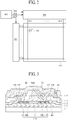
- FIG. 2 is an exemplary diagram illustrating a configuration of a display device according to an embodiment of the present disclosure.
- the display device may include a display panel 100 where a plurality of pixels (P) 110 defined by a plurality of gate lines GL1 to GLg and a plurality of data lines DL1 to DLd are provided to display an image.
- the display device may also include a gate driver 200 that sequentially supplies a gate pulse to the gate lines GL1 to GLg included in the panel 100, a data driver 300 that respectively supplies data voltages to the data lines DL1 to DLd included in the panel 100, and a controller 400 that controls the gate driver 200 and the data driver 300.
- the display panel 100 may include the gate lines GL1 to GLg supplied with the gate pulse, the data lines DL1 to DLd supplied with the data voltages, and the pixels 110 defined by the gate lines GL1 to GLg and the data lines DL1 to DLd.
- the pixels 110 may each include at least one coplanar type oxide TFT (hereinafter simply referred to as an "oxide TFT") according to an embodiment of the present disclosure. A configuration and a function of the oxide TFT will be described in detail with reference to FIGS. 3 to 12 .
- the display panel 100 may be a liquid crystal display panel applied to LCD devices, or may be an organic light emitting display panel applied to organic light emitting display devices.
- each of the pixels 110 included in the display panel 100 may include one oxide TFT used as a switching element for driving the liquid crystals.
- each of the pixels 110 included in the display panel 100 may include an organic light emitting diode (OLED) emitting light and a pixel driver for driving the OLED.
- OLED organic light emitting diode
- the pixel driver may be configured with two or more TFTs for driving the OLED.
- the TFTs included in the pixel driver may be oxide TFTs.
- the oxide TFTs may also be provided in a non-display area outside the display area where the pixels 110 are provided. Therefore, all TFTs included in the display panel 100 may be formed through the same process.
- TFTs configuring the gate driver 200 may each be configured as an oxide TFT.
- the controller 400 may generate and output a gate control signal GCS for controlling the gate driver 200 and a data control signal DCS for controlling the data driver 300 by using a vertical synchronization signal, a horizontal synchronization signal, and a clock which are supplied from an external system.
- controller 400 may sample input video data received from the external system, realign the sampled video data to generate digital image data Data, and supply the digital image data to the data driver 300.
- the data driver 300 may convert the image data Data input from the controller 400 into analog data voltages and may respectively supply the data voltages for one horizontal line to the data lines DL1 to DLd at every one horizontal period where the gate pulse is supplied to one gate line GL.
- the gate driver 200 may sequentially supply the gate pulse to the gate lines GL1 to GLg in response to the gate control signal GCS input from the controller 400. Therefore, oxide TFTs provided in each of pixels to which the gate pulse is input may be turned on, and thus, each of the pixels 110 may display an image.
- the gate driver 200 may be provided independently from the panel 100 and may be electrically connected to the panel 100 in various ways.
- the gate driver 200 may be provided in a gate-in panel (GIP) type which is mounted in the non-display area of the display panel 100.
- GIP gate-in panel
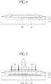
- FIG. 3 is a cross-sectional view of a coplanar type oxide TFT according to an embodiment of the present disclosure.
- the display device may include the display panel 100, and at least one coplanar type oxide TFT according to an embodiment of the present disclosure, like as illustrated in FIG. 3 , may be included in each of the plurality of pixels provided in the display area of the display panel 100.
- the oxide TFT according to an embodiment of the present disclosure may include a semiconductor layer CH formed of oxide semiconductor material provided on a buffer 112 deposited on a substrate 111, a gate insulation layer 113 which covers the semiconductor layer CH and the buffer 112, a gate electrode Gate which is provided on the gate insulation layer 113 and overlaps at least a portion of the semiconductor layer CH, and a passivation layer 114 that covers the gate electrode Gate and the gate insulation layer 113.
- a resistance of an area of the semiconductor layer CH overlapping the gate electrode Gate may differ from a resistance of an area outside the overlapping area.
- a TFT having a type where the gate is disposed on the semiconductor layer CH may be referred to as a coplanar type TFT.
- the buffer 112 may be disposed on the substrate 111.
- the buffer 112 may be formed of an organic material or an inorganic material, formed of a combination thereof, and formed of at least one layer.
- the buffer 12 may include SiO 2 , and a thickness of the buffer 112 may be adjusted to 100 nm to 1 ⁇ m.
- a light shielding layer LS for blocking light incident on the semiconductor layer CH may be further provided between the substrate 111 and the buffer 112.
- an end of the light shielding layer LS may have an inclined surface from the top surface of the light shielding layer LS to the bottom surface of the light shielding layer LS.
- the buffer 112 may be deposited along the inclined surface of the light shielding layer LS with a uniform thickness such that the buffer 112 also has an inclined surface.
- the gate insulation layer 113 may also cover the portion of the buffer 112 having the inclined surface.
- the gate insulation layer 113 may not be etched, and thus, the buffer 112 may not be damaged by an etching process.
- an etching process for etching the gate insulation layer 113 may also damage or etch a portion of the buffer 112 covering the light shielding layer LS, including the inclined surface of the buffer 112. This can result in a short circuit between the gate electrode Gate and the light shielding layer LS. Since the gate insulation layer 113 is not etched, the gate insulation layer 113 can cover the buffer 112 such that a short circuit between the gate electrode Gate and the light shielding layer LS can be prevented.
- the semiconductor layer CH may be formed of an oxide semiconductor.
- the oxide semiconductor may be indium-gallium zinc oxide (IGZO) consisting of indium (In), gallium (Ga), zinc (Zn), and oxygen (O).
- the oxide semiconductor may include tin (Sn), hafnium (Hf), magnesium (Mg), aluminum (Al), or zirconium (Zr).
- the semiconductor layer CH may include an active area A formed of the oxide semiconductor, a first conductor C1 which is provided adjacent to one end of the active area A in the semiconductor layer CH and has a sheet resistance lower than that of the active area A, and a second conductor C2 which is provided adjacent to the other end of the active area A in the semiconductor layer CH and has a sheet resistance lower than that of the active area A.
- the active area A may be aligned with the gate electrode Gate, or may be aligned with the light shielding layer LS disposed below the buffer 112. That is a width of the active area A is aligned with a width of the gate electrode Gate in one embodiment and in another embodiment the width of the active area A is aligned with the width of the light shielding layer LS.
- the first conductor C1 may be connected to a first electrode E1, and the second conductor C2 may be connected to a second electrode E2.
- the oxide TFT is a TFT provided in each pixel of a liquid crystal display panel
- the first electrode E1 may be connected to a data line
- the second electrode E2 may be connected to a pixel electrode PE included in the pixel.
- the gate electrode Gate may be connected to a gate line.
- the first conductor C1 may include metal that is included in the oxide semiconductor, and the metal included in the first conductor C1 may have free electrons and a vacancy from which oxygen is separated.
- the second conductor C2 may include a metal included in the oxide semiconductor, and the metal included in the second conductor C2 may have free electrons and a vacancy from which oxygen is separated.
- the covalent bond between the metal and the oxygen may be broken and oxygen vacancies may be created. Accordingly, free electrons may be generated in the metal.
- An area where the free electron is generated through exposure to UV radiation may be the first conductor C1 and/or the second conductor C2. Due to the free electrons generated in the first conductor C1 and/or the second conductor C2, mobility of each of the first conductor C1 and the second conductor C2 may be greater than mobility of the active area A consisting of the oxide semiconductor. Also, due to the free electrons generated in the first conductor C1 and/or the second conductor C2, resistance of each of the first conductor C1 and the second conductor C2 may be smaller than the resistance of the active area A consisting of the oxide semiconductor.
- the first conductor C1 and the second conductor C2 may have characteristics of a conductor. As described above, the first conductor C1 may be electrically connected to the first electrode E1, and the second conductor C2 may be electrically connected to the second electrode E2.
- metal included in the oxide semiconductor may be bonded to a hydroxy group (-OH) from the gate insulation layer 113 to form a first metal layer ML1 that contacts the gate insulation layer 113.
- metal included in the oxide semiconductor may be bonded to a hydroxyl group (-OH) from the gate insulation layer 113 to generate a second metal layer ML2 that contacts the gate insulation layer 113.
- the gate insulation layer 113 may include SiO 2 .
- the gate electrode Gate may be provided on the gate insulation layer 113.
- the gate electrode Gate may overlap the active area A consisting of the oxide semiconductor in the semiconductor layer CH.
- the first conductor C1 and the second conductor C2 may not overlap the gate electrode Gate.
- the gate insulation layer 113 may be provided on the semiconductor layer CH, and the gate electrode Gate may be provided on the gate insulation layer 113. Subsequently, when the UV is irradiated onto an upper side of each of the gate electrode Gate and the gate insulation layer 113, as described above, both ends of the active area A may not be covered by the gate electrode Gate consisting of metal, and for this reason, the UV may be irradiated onto both ends of the active area A via the gate insulation layer 113. Therefore, the active area A may be aligned with the gate electrode Gate, and both ends of the active area A may become conductive, and thus, the first and second conductors C1 and C2 may be formed. Alternatively when the UV light is irradiated from below the substrate, the active area A may be aligned with the light shielding layer LS, and both ends of the active area A may become conductive to form the first and second conductors C1 and C2.
- the passivation layer 114 that covers the gate electrode Gate and the gate insulation layer 113 may be provided on the gate electrode Gate and the gate insulation layer 113.
- the passivation layer 114 may include SiO 2 .
- an oxygen concentration at a surface portion of the oxide semiconductor constituting the semiconductor layer CH may vary from 1% to 5%.
- the first electrode E1 provided on the passivation layer 114 may be connected to the first conductor C1 through a first contact hole formed in the passivation layer 114 and a second contact hole formed in the gate insulation layer 113 that is aligned with the first contact hole, and the second electrode E2 may be connected to the second conductor C2 through a third contact hole formed in the passivation layer 114 and a fourth contact hole formed in the gate insulation layer 113 that is aligned with the third contact hole.
- the passivation layer 114, the first electrode E1, and the second electrode E2 may be covered by an insulation layer 115.
- An electrode layer which is connected to the second electrode E2 through a contact hole formed in the insulation layer 115 may be formed on the insulation layer 115.
- the electrode layer as described above, may be a pixel electrode PE.
- FIGS. 4 to 7 are exemplary diagrams illustrating a method of manufacturing a coplanar type oxide TFT according to an embodiment of the present disclosure.
- FIG. 8 is an exemplary diagram illustrating another coplanar type oxide TFT applied to an organic light emitting display panel according to an embodiment of the present invention.
- the light shielding layer LS, the buffer 112, the semiconductor layer CH, and the gate insulation layer 113 may be sequentially stacked on the substrate 111.
- the light shielding layer LS may be formed such that an end of the light shielding layer LS has an inclined surface.
- the buffer 112 may be deposited along the light shielding layer LS with uniform thickness such that a portion of the buffer 112 also has an inclined surface.
- the gate insulation layer 113 may cover the portion of the buffer 112 having the inclined surface.
- the light shielding layer LS may be omitted.
- All areas of the semiconductor layer CH may consist of an oxide semiconductor such as IGZO or the like.
- the gate electrode Gate may be coated on an area corresponding to the semiconductor layer CH.
- the gate electrode Gate may overlap with a center portion of the semiconductor layer CH without overlapping the whole semiconductor layer CH. Therefore, both ends of the semiconductor layer CH may not overlap the gate electrode Gate.
- the gate electrode Gate may be provided, and then, the UV may be irradiated onto the gate electrode Gate and the gate insulation layer 113. In this case, as illustrated in FIG. 5 , the UV may be irradiated onto an upper side of each of the gate insulation layer 113 and the gate electrode Gate.
- a resistance of a first area of the semiconductor layer CH that does not overlap the gate electrode Gate is decreased to form the first conductor C1
- a resistance of a second area of the semiconductor layer CH at the opposite end of the first area that does not overlap with the gate electrode Gate is decreased to form the second conductor C2.
- the active area A is formed in between the first conductor C1 and the second conductor C2, and is aligned with the gate electrode Gate, and the first conductor C1 is formed adjacent to a first end of the active area A, and the second conductor C2 is formed adjacent to a second area of the active area A.
- the UV may be irradiated from below the substrate 111.
- the light shielding layer LS is formed smaller than the semiconductor layer CH, and particularly, formed in a size similar to that of the gate electrode Gate, areas of the semiconductor layer CH which is not covered by the light shielding layer LS may become conductive when the UV is irradiated through the lower side of the substrate 111, thereby forming the first conductor C1 and the second conductor C2. That is, the width of the light shielding layer may be less than that of the semiconductor layer.
- the active area A may be formed in between the first conductor C1 and the second conductor C2 to be aligned with the light shielding layer LS.
- the light shield LS may be formed greater or less than the gate Gate.
- the light shield LS may be formed to have the same size as that of the gate Gate and may be disposed to overlap the gate Gate.
- the UV irradiation may include UV rays having a wavelength 185 nm and UV rays having a wavelength of 254nm.
- the oxide semiconductor may become conductive by the UV, and thus, the first conductor C1 and the second conductor C2 may be formed.
- a wavelength of the UV rays may be within a range from 100 nm to 400nm.
- the first metal layer ML1 may be formed in a boundary area between the first conductor C1 and the gate insulation layer 113 to contact the gate insulation layer 113
- the second metal layer ML2 may be formed in a boundary area between the second conductor C2 and the gate insulation layer 113 to contact the gate insulation layer 113, as shown in FIG. 6 .
- the passivation layer 114 may cover the gate insulation layer 113 and the gate electrode Gate.
- a first contact hole 155 is formed through the passivation layer 114 and a second contact hole 156 is formed through the gate insulation layer 113 to expose at least a portion of the first conductor C1.
- the first contact hole 155 and the second contact hole 156 may be formed simultaneously.
- a third contact hole 157 is formed through the passivation layer 114 and a fourth contact hole 158 is formed through the gate insulation layer 113 to expose at least a portion of the second conductor C2.
- the third contact hole 157 and the fourth contact hole 158 may be formed simultaneously.
- the first electrode E1 provided on the gate insulation layer 113 may be connected to the first conductor C1 through the first contact hole 155 formed in the passivation layer 114 and the second contact hole 156 formed in the gate insulation layer 113, and the second electrode E2 provided on the gate insulation layer 113 may be connected to the second conductor C2 through the third contact hole 157 formed in the passivation layer 114 and the fourth contact hole 158 formed in the gate insulation layer 113.
- the insulation layer 115 may cover the first electrode E1, the second electrode E2, and the passivation layer 114.
- FIG. 9 is an exemplary diagram illustrating a method of forming the first conductor C1 and the second conductor C2 of the coplanar type oxide TFT according to an embodiment of the present disclosure.
- the UV when the UV is irradiated onto the semiconductor layer CH consisting of the oxide semiconductor such as IGZO or the like, a bond between oxygen (O 2- ) and metal M constituting the oxide semiconductor may be broken, and the oxygen (O 2- ) may be dissociated from the metal M. In this case, free electrons may be generated due to the oxygen vacancies. Accordingly, the first conductor C1 and the second conductor C2 where the free electrons are generated may be respectively provided at both ends of the semiconductor layer CH. In other words, carriers may be generated in an area of the oxide semiconductor into which the UV is irradiated, and thus, a resistance of the area is rapidly reduced, whereby the area may have characteristics of a conductor.
- the oxide semiconductor such as IGZO or the like
- Oxygen (O 2- ) dissociated from the metal M may bond to each other to generate an oxygen molecule, and the oxygen molecule may be trapped in the gate insulation layer 113 or may be discharged externally through the gate insulation layer 113.
- water (H 2 O) remaining in the gate insulation layer 113 or water (H 2 O) in the air may be photo dissociated into an H group and an OH group by the UV irradiation.
- the metal M from which the oxygen (O 2- ) is dissociated may bond to the OH group in a boundary area between the first conductor C1 and the gate insulation layer 113 to form the first metal layer ML1, and the metal M from which the oxygen (O 2- ) is dissociated may bond to the OH group in a boundary area between the second conductor C2 and the gate insulation layer 113 to form the second metal layer ML2.
- a mobility of the first conductor C1 increases due to the first metal layer ML1 and the free electrons, and thus, a resistance is reduced.
- a mobility of the second conductor C2 increases due to the second metal layer ML2 and the free electrons, and thus, a resistance is reduced.
- oxygen may be physically dissociated through dry etching and plasma.
- the oxide semiconductor for example, IGZO
- the oxide semiconductor may be changed to a conductor.
- oxygen may be physically dissociated from the metal in the oxide semiconductor by using the UV rays instead of dry etching and plasma.
- oxygen defects occur in a metal oxide semiconductor such as IGZO 4 , and thus, the metal oxide semiconductor may be changed to IG-ZO 4-x , and oxygen vacancies may supply free electrons.
- the vacancy of the oxygen may be bonded to an OH group to form an MOH bond, whereby the vacancy of the oxygen cannot be bonded to oxygen again.
- the energy difference between the conduction band and the valance band may be about 250 lambda when the difference is converted to a wavelength range. Due to a dangling bond state between the conduction band and the valance band, when UV rays having a wavelength of 400 lambda or less is irradiated, oxygen vacancies may be formed due to dissociation of oxygen. Therefore, UV rays having a wavelength of 100 lambda to 400 lambda is appropriate to dissociate the oxygen.
- FIG. 10 is a graph showing a result obtained by comparing the device characteristic of a coplanar type oxide TFT according to an embodiment of the present disclosure with the device characteristics of a coplanar type oxide TFT which has a structure similar to an embodiment of the present disclosure but on which ultraviolet (UV) is not irradiated.
- reference numeral X refers to characteristic of an oxide semiconductor which is not processed by UV irradiation although the oxide semiconductor has a structure where a gate insulation layer is not etched similarly to an oxide semiconductor according to an embodiment of the present disclosure.
- Reference numeral Y refers to characteristic of the oxide semiconductor according to an embodiment of the present disclosure which has a structure illustrated in FIG. 3 and has been processed by UV irradiation.
- a structure where a gate insulation layer is not etched is good in terms of reducing defects, but if UV treatment is not performed, resistances of both ends of the semiconductor layer increase greatly. Therefore, a very high resistance may be applied between the first electrode E1 and the semiconductor layer, and thus, a current may be cut off. Accordingly, mobility is greatly reduced as shown in the characteristics of the graph referred to by X, and for this reason, it is difficult to use the oxide semiconductor for which the UV treatment is not performed.
- the resistance characteristics of the first and second conductors C1 and C2 improve as shown in characteristics of the graph referred to by Y. Therefore, an on current increases in the oxide semiconductor for which the UV treatment has been performed.
- UV (185nm+254nm) may be irradiated onto the gate electrode Gate and the gate insulation layer 113.
- thermal processing of 100°C to 200°C (for example, heat of 150°C) may be applied under the substrate 111 simultaneously with the UV irradiation.
- both ends of the semiconductor layer CH may become conductive, and thus, the first and second conductors C1 and C2 may be formed.
- a mobility of the semiconductor layer CH before the both ends of the semiconductor layer CH become conductive is 4.5 cm 2 /Vs, and a current is cut off by a resistance of the semiconductor layer CH.
- both ends of the semiconductor layer CH become conductive due to UV irradiated thereon, and a mobility of each of the first and second conductors C1 and C2 is enhanced to 15 cm 2 /Vs. Therefore, it can be seen that the device performance of the oxide semiconductor is enhanced by 300% or more. In this case, when thermal processing is applied to the oxide semiconductor, characteristics of the first and second conductors C1 and C2 are more stabilized. Accordingly, an oxide semiconductor with enhanced reliability is manufactured.
- the graph referred to by X shows a relationship between a gate-source voltage Vgs and a drain-source current Ids in an oxide semiconductor which has a structure similar to a structure according to an embodiment of the present disclosure but where UV is not irradiated onto both ends of a semiconductor layer
- the graph referred to by Y shows a relationship between a gate-source voltage Vgs and a drain-source current Ids in the oxide semiconductor according to an embodiment of the present disclosure.
- the drain-source current Ids in the oxide semiconductor according to an embodiment of the present disclosure increases.
- FIG. 11 is a graph showing a relationship between a current and a duration for which UV is irradiated onto a coplanar type oxide TFT according to an embodiment of the present disclosure.
- FIG. 12 is a graph showing a relationship between Hall mobility, carrier concentration, and a duration for which UV is irradiated onto a coplanar type oxide TFT according to an embodiment of the present disclosure.
- a Hall mobility and a carrier concentration of the oxide semiconductor according to an embodiment of the present disclosure increase.
- a graph showing the hall mobility is referred to by T
- a graph showing the carrier concentration is referred to by S.
- the resistance characteristic of an oxide semiconductor is controlled by a photo-chemical method without vacuum dry etching (D/E) equipment.
- merits of the related art coplanar type oxide TFT may be retained, a process of manufacturing a coplanar type oxide TFT is simplified, the device characteristic of the coplanar type oxide TFT is improved, and a defect issue is reduced.
- a short circuit between a gate and a drain can occur due to a foreign material introduced when etching the gate insulation layer.
- the gate insulation layer is not etched, a possibility that a short circuit is created between a gate and a drain is reduced.
- the gate insulation layer is not etched, thereby preventing a short circuit defect which occurs between the light shielding layer and conductive lines because the buffer is etched when etching the gate insulation layer.
- the gate insulation layer is etched, and then, end portions of a semiconductor layer formed of oxide semiconductor become conductive by using plasma, thereby manufacturing the coplanar type oxide TFT.
- the gate insulation layer may not be etched.
- UV irradiation 185nm+254nm
- thermal processing 150°C
- a process of etching the gate insulation layer may be omitted, and the end portions of the semiconductor layer formed of oxide (IGZO) may become conductive by using the photo-chemical method, thereby manufacturing the coplanar type TFT.
- IGZO oxide
Landscapes
- Physics & Mathematics (AREA)
- Nonlinear Science (AREA)
- Engineering & Computer Science (AREA)
- Microelectronics & Electronic Packaging (AREA)
- Crystallography & Structural Chemistry (AREA)
- Chemical & Material Sciences (AREA)
- Mathematical Physics (AREA)
- General Physics & Mathematics (AREA)
- Optics & Photonics (AREA)
- Geometry (AREA)
- Thin Film Transistor (AREA)
- Electroluminescent Light Sources (AREA)
- Liquid Crystal (AREA)
Abstract
Description
- This application claims the benefit of Republic of Korea Patent Application No.
10-2016-0083097 filed on June 30, 2016 - The present invention relates to a coplanar type oxide thin film transistor (TFT), a method of manufacturing the same, and a display panel and a display device using the same.
- A flat panel display (FPD) device is applied to various electronic devices such as portable phones, tablet personal computers (PCs), notebook computers, monitors, etc. Examples of FPD apparatuses include liquid crystal display (LCD) devices, plasma display panel (PDP) devices, organic light emitting display devices, etc. Recently, electrophoretic display (EPD) devices are being widely used as one type of the FPD device.
- In FPD devices, LCD devices display an image by using liquid crystal, and organic light emitting display devices use a self-emitting device that self-emits light.
- A display panel configuring a display device includes a plurality of switching elements, for displaying an image. The switching elements may be configured with thin film transistors (TFTs). Each of the TFTs may be formed of amorphous silicon (a-Si), poly silicon, or oxide. A TFT formed of oxide is referred to as an oxide TFT.
-
FIG. 1 is an exemplary diagram illustrating a process of manufacturing a related art coplanar type oxide TFT. - First, as illustrated in
FIG. 1 (a) , abuffer 12 is coated on asubstrate 11, anoxide semiconductor 13 is coated on an upper side of thebuffer 12, agate insulation layer 14 is coated on theoxide semiconductor 13, and a patternedgate 15 is stacked on an upper side of thegate insulation layer 14. When thegate insulation layer 14 is etched by using thegate 15 as a mask, as illustrated inFIG. 1 (b) , a portion of theoxide semiconductor 13 is exposed. - In this case, as illustrated in
FIG. 1 (b) , when plasma is irradiated onto the exposed portion of theoxide semiconductor 13, the exposed area becomes conductive, and thus, afirst electrode 16 and asecond electrode 17 of the oxide TFT are formed. One of thefirst electrode 16 and thesecond electrode 17 is a source of the oxide TFT, and the other electrode is a drain of the oxide TFT. - As described above, the
gate insulation layer 14 is etched through a dry etching process, and then, the exposed portion of theoxide semiconductor 13 becomes conductive by plasma treatment, thereby manufacturing thefirst electrode 16 and thesecond electrode 17 of the related art coplanar type oxide TFT. - However, since the
gate insulation layer 14 is etched through a dry etching process for forming thefirst electrode 16 and thesecond electrode 17, thebuffer 12 is etched in the dry etching process, and for this reason, a step height K can occur between the oxide semiconductor 13a and thebuffer 12. Due to the step height K, a short circuit defect can occur in lines connected between thefirst electrode 17 and thesecond electrode 16. - Moreover, in depositing an insulation layer in a subsequent process, due to the step height K, step coverage problems can occur, and the
gate 15 and the drain may be shortcircuited with each other, causing a short circuit defect. For this reason, the reliability of a TFT is degraded. - Moreover, when the
gate insulation layer 14 is over-etched, a portion of thebuffer 12 may be damaged or removed. - In addition, if a light shielding layer for blocking light is provided between the
substrate 11 and thebuffer 12, and thegate insulation layer 14 and thebuffer 12 are over-etched, the light shielding layer can be exposed or the thickness of thebuffer 12 may be reduced, causing a short circuit between the light shielding layer and thegate 15. - Thus, in order to manufacture the related art coplanar type oxide TFT, the
gate insulation layer 14 should be etched through the dry etching process, and due to the dry etching process, various kinds of defects can occur. - The above identified problems are solved by the features of the independent claims. Accordingly, the present disclosure is directed to provide a coplanar type oxide thin film transistor (TFT), a method of manufacturing the same, and a display panel and a display device using the same that substantially obviate one or more problems due to limitations and disadvantages of the related art.
- An aspect of the present disclosure is directed to provide a coplanar type oxide TFT, a method of manufacturing the same, and a display panel and a display device using the same, in which a first conductor and a second conductor are provided at end portions of a semiconductor layer formed of oxide semiconductor, electrically connected to a first electrode and a second electrode, and covered by a gate insulation layer.
- Additional advantages and features of the invention will be set forth in part in the description which follows and in part will become apparent to those having ordinary skill in the art upon examination of the following or may be learned from practice of the invention. The objectives and other advantages of the invention may be realized and attained by the structure particularly pointed out in the written description and claims hereof as well as the appended drawings.
- In an exemplary embodiment, there is provided a coplanar type oxide TFT including a semiconductor layer provided on a buffer, the semiconductor layer including an oxide semiconductor, a gate insulation layer covering the semiconductor layer and the buffer, a gate provided on the gate insulation layer to overlap a portion of the semiconductor layer, and a passivation layer covering the gate and the gate insulation layer, wherein a resistance of an area of the semiconductor layer overlapping the gate differs from a resistance of an area other than the overlapping area.
- In an exemplary embodiment, the active area is aligned with the gate electrode.
- In an exemplary embodiment, the oxide TFT comprises a light shielding layer below the buffer.
- In an exemplary embodiment, the active area is aligned with the light shielding layer.
- In an exemplary embodiment, a portion of the buffer covering an end of the light shielding layer has an inclined surface.
- In an exemplary embodiment, the gate insulation layer covers the portion of the buffer.
- In an exemplary embodiment, the resistance of the first conductor is lower than the resistance of the active area.
- In an exemplary embodiment, the resistance of the second conductor is lower than the resistance of the active area.
- In an exemplary embodiment, the first conductor comprises a same metal that is included in the oxide semiconductor material
- In an exemplary embodiment, the metal included in the first conductor comprises a free electron and an oxygen vacancy.
- In an exemplary embodiment, the second conductor comprises the same metal as the first conductor
- In an exemplary embodiment, the metal in the second conductor comprises a free electron and an oxygen vacancy.
- In an exemplary embodiment, the oxide TFT further comprises a first metal layer contacting the gate insulation layer, wherein the first metal layer comprises a same metal that is included in the oxide semiconductor material bonded to a hydroxy group (-OH).
- In an exemplary embodiment, the second conductor comprises a second metal layer contacting the gate insulation layer, wherein the second metal layer comprises the metal bonded to a hydroxy group (-OH).
- In an exemplary embodiment, the oxide TFT further comprises a first electrode of the oxide TFT contacting the first conductor through a first contact hole in the gate insulation layer and a second contact hole in the passivation layer, wherein the first contact hole and the second contact hole are aligned.
- In an exemplary embodiment, the oxide TFT further comprises a second electrode of the oxide TFT contacting the second conductor through a third contact hole in the gate insulation layer and a fourth contact hole in the passivation layer, wherein the third contact hole and the fourth contact hole are aligned.
- In an exemplary embodiment, a number of oxygen vacancies in the first conductor is greater than a number of oxygen vacancies in the active area,
- In an exemplary embodiment, a number of oxygen vacancies in the second conductor is greater than the number of oxygen vacancies in the active area.
- In an exemplary embodiment, a display panel comprises a plurality of gate lines that receive a plurality of gate pulses; a plurality of data lines that receive a plurality of data voltages; and a plurality of pixels defined by the plurality of gate lines and the plurality of data lines, wherein each of the plurality of pixels comprises an oxide thin film transistor (TFT) according to the above-mentioned manner. This oxide TFT comprises a semiconductor layer provided on a buffer, the semiconductor layer including an oxide semiconductor material and comprising an active area, a first conductor adjacent to a first end of the active area, and a second conductor adjacent to a second end of the active area; a gate insulation layer covering the semiconductor layer and the buffer; a gate electrode provided on the gate insulation layer and overlapping a portion of the semiconductor layer; and a passivation layer covering the gate electrode and the gate insulation layer, a resistance of the active area is different from a resistance of the first conductor and a resistance of the second conductor.
- In an exemplary embodiment of the display panel, the active area is aligned with the gate electrode.
- In an exemplary embodiment, the display panel further comprises a light shielding layer below the buffer.
- In an exemplary embodiment, the display panel further comprises the active area is aligned with the light shielding layer.
- In an exemplary embodiment of the display panel, a portion of the buffer covering an end of the light shielding layer has an inclined surface
- In an exemplary embodiment, the display panel further comprises the gate insulation layer covers the portion of the buffer.
- In an exemplary embodiment of the display panel, the oxide TFT is provided in a non-display area outside a display area where the plurality of pixels is provided.
- In an exemplary embodiment, there is provided a method of manufacturing an oxide thin film transistor (TFT), preferably a coplanar type oxide TFT, including depositing a buffer on a substrate, forming a semiconductor layer including an oxide semiconductor in the buffer, depositing a gate insulation layer to cover the semiconductor layer and the buffer, depositing a gate, overlapping a portion of the semiconductor layer, on the gate insulation layer, and decreasing a resistance of a first area and a second area of the semiconductor layer, wherein the first area is at a first end of an active area of the semiconductor layer and wherein the second area is at a second end of the active area of the semiconductor layer, the first area with the decreased resistance forming a first conductor and the second area with the decreased resistance forming a second conductor while the gate insulation layer is covering the semiconductor layer and the buffer. The decreasing of the resistance of the first area and the second area comprises irradiating ultraviolent (UV) light to cause an area of the semiconductor layer, which does not overlap the gate, to become conductive.
- In an exemplary embodiment, the decreasing of the resistance of the first area and the second area comprises irradiating ultraviolent (UV) light on the semiconductor layer.
- According to an exemplary embodiment, the active area is aligned with the gate electrode in response to the UV light being irradiated on the gate electrode.
- In an exemplary embodiment, the method further comprises forming a light shielding layer below the buffer, and in response to the UV light being irradiated from below the substrate, the active area is aligned with the light shielding layer.
- In an exemplary embodiment, the method further comprises thermally processing the semiconductor layer simultaneously with the irradiating of the UV or after the irradiating of the UV.
- In an exemplary embodiment, the method further comprises depositing a passivation layer that covers the gate insulation layer and the gate; simultaneously forming a first contact hole and a second contact hole respectively through the passivation layer and the gate insulation layer, and a third contact hole and a fourth contact hole respectively through the passivation layer and the gate insulation layer, wherein the first contact hole and the second contact hole are aligned, and wherein the third contact hole and the fourth contact hole are aligned; and forming a first electrode of the oxide TFT contacting the first conductor through the first contact hole and the second contact hole, and forming a second electrode of the oxide TFT contacting the second conductor through the third contact hole and the fourth contact hole.
- An exemplary embodiment relates to an oxide TFT including a semiconductor layer provided on a buffer. The semiconductor layer includes an oxide semiconductor material, and includes an active area, a first conductor adjacent to a first end of the active area, and a second conductor adjacent to a second end of the active area. The oxide TFT also includes a gate insulation layer covering the semiconductor layer and the buffer, a gate electrode provided on the gate insulation layer and overlapping a portion of the semiconductor layer, and a passivation layer covering the gate electrode and the gate insulation layer. A resistance of the active area is different from a resistance of the first conductor and a resistance of the second conductor.
- An exemplary embodiment also relates to a display panel comprising a plurality of gate lines that receive a plurality of gate pulses, a plurality of data lines that receive a plurality of data voltages, and a plurality of pixels defined by the plurality of gate lines and the plurality of data lines. Each of the plurality of pixels includes an oxide TFT including a semiconductor layer provided on a buffer, in which the semiconductor layer includes an oxide semiconductor material, and includes an active area, a first conductor adjacent to a first end of the active area, and a second conductor adjacent to a second end of the active area. The oxide TFT also includes a gate insulation layer covering the semiconductor layer and the buffer, a gate electrode provided on the gate insulation layer and overlapping a portion of the semiconductor layer, a passivation layer covering the gate electrode and the gate insulation layer. A resistance of the active area is different from a resistance of the first conductor and a resistance of the second conductor.
- An exemplary embodiment also relates to a method of manufacturing an oxide TFT. A buffer is deposited on a substrate. A semiconductor layer including an oxide semiconductor material is formed on the buffer. A gate insulation layer is deposited to cover the semiconductor layer and the buffer, and a gate electrode is deposited on the gate insulation layer. A resistance of a first area of the semiconductor layer adjacent to a first end of an active area of the semiconductor layer and a second area of the semiconductor layer adjacent to a second end of the active area is decreased. The first area with the decreased resistance forms a first conductor and the second area with the decreased resistance forms a second conductor while the gate insulation layer is covering the semiconductor layer and the buffer.
- It is to be understood that both the foregoing general description and the following detailed description of the present invention are exemplary and explanatory and are intended to provide further explanation of the invention as claimed.
- The accompanying drawings, which are included to provide a further understanding of the invention and are incorporated in and constitute a part of this application, illustrate embodiments of the invention and together with the description serve to explain the principle of the invention. In the drawings:
-
FIG. 1 is an exemplary diagram illustrating a process of manufacturing a related art coplanar type oxide TFT; -
FIG. 2 is an exemplary diagram illustrating a configuration of a display device according to an embodiment of the present disclosure; -
FIG. 3 is a cross-sectional view of a coplanar type oxide TFT according to an embodiment of the present disclosure; -
FIGS. 4 to 7 are exemplary diagrams illustrating a method of manufacturing a coplanar type oxide TFT according to an embodiment of the present disclosure; -
FIG. 8 is an exemplary diagram illustrating another coplanar type oxide TFT applied to an organic light emitting display panel according to an embodiment of the present invention; -
FIG. 9 is an exemplary diagram illustrating a method of forming a first conductor and a second conductor of a coplanar type oxide TFT according to an embodiment of the present disclosure; -
FIG. 10 is a graph showing a result obtained by comparing the device characteristics of a coplanar type oxide TFT according to an embodiment of the present disclosure with the device characteristic of a coplanar type oxide TFT which has a structure similar to an embodiment of the present disclosure but on which ultraviolet (UV) is not irradiated; -
FIG. 11 is a graph showing a relationship between a current and a duration for which UV is irradiated onto a coplanar type oxide TFT according to an embodiment of the present disclosure; and -
FIG. 12 is a graph showing a relationship between Hall mobility, carrier concentration, and a duration for which UV is irradiated onto a coplanar type oxide TFT according to an embodiment of the present disclosure. - Reference will now be made in detail to the exemplary embodiments of the present disclosure, examples of which are illustrated in the accompanying drawings. Wherever possible, the same reference numbers will be used throughout the drawings to refer to the same or like parts.
- Advantages and features of the present invention, and implementation methods thereof will be clarified through following embodiments described with reference to the accompanying drawings. The present invention may, however, be embodied in different forms and should not be construed as limited to the embodiments set forth herein. Rather, these embodiments are provided so that this disclosure will be thorough and complete, and will fully convey the scope of the present invention to those skilled in the art. Furthermore, the present invention is only defined by scopes of claims.
- In the specification, in adding reference numerals for elements in each drawing, it should be noted that like reference numerals already used to denote like elements in other drawings are used for elements wherever possible.
- A shape, a size, a ratio, an angle, and a number disclosed in the drawings for describing embodiments of the present invention are merely an example, and thus, the present invention is not limited to the illustrated details. Like reference numerals refer to like elements throughout. In the following description, when the detailed description of the relevant known function or configuration is determined to unnecessarily obscure the important point of the present invention, the detailed description will be omitted. In a case where 'comprise', 'have', and 'include' described in the present specification are used, another part may be added unless 'only-' is used. The terms of a singular form may include plural forms unless referred to the contrary.
- In construing an element, the element is construed as including an error range although there is no explicit description.
- In describing a position relationship, for example, when a position relation between two parts is described as 'on-', 'over-', 'under-', and 'next-', one or more other parts may be disposed between the two parts unless 'just' or 'direct' is used.
- In describing a time relationship, for example, when the temporal order is described as 'after-', 'subsequent-', 'next-', and 'before-', a case which is not continuous may be included unless 'just' or 'direct' is used.
- The term "at least one" should be understood as including any and all combinations of one or more of the associated listed items. For example, the meaning of "at least one of a first item, a second item, and a third item" denotes the combination of all items proposed from two or more of the first item, the second item, and the third item as well as the first item, the second item, or the third item.
- It will be understood that, although the terms "first", "second", etc. may be used herein to describe various elements, these elements should not be limited by these terms. These terms are only used to distinguish one element from another. For example, a first element could be termed a second element, and, similarly, a second element could be termed a first element, without departing from the scope of the present invention.
- Features of various embodiments of the present invention may be partially or overall coupled to or combined with each other, and may be variously inter-operated with each other and driven technically as those skilled in the art can sufficiently understand. The embodiments of the present invention may be carried out independently from each other, or may be carried out together in co-dependent relationship.
- Hereinafter, embodiments of the present disclosure will be described in detail with reference to the accompanying drawings.
-
FIG. 2 is an exemplary diagram illustrating a configuration of a display device according to an embodiment of the present disclosure. - As illustrated in
FIG. 2 , the display device according to an embodiment of the present disclosure may include adisplay panel 100 where a plurality of pixels (P) 110 defined by a plurality of gate lines GL1 to GLg and a plurality of data lines DL1 to DLd are provided to display an image. The display device may also include agate driver 200 that sequentially supplies a gate pulse to the gate lines GL1 to GLg included in thepanel 100, adata driver 300 that respectively supplies data voltages to the data lines DL1 to DLd included in thepanel 100, and acontroller 400 that controls thegate driver 200 and thedata driver 300. - The
display panel 100 may include the gate lines GL1 to GLg supplied with the gate pulse, the data lines DL1 to DLd supplied with the data voltages, and the pixels 110 defined by the gate lines GL1 to GLg and the data lines DL1 to DLd. The pixels 110 may each include at least one coplanar type oxide TFT (hereinafter simply referred to as an "oxide TFT") according to an embodiment of the present disclosure. A configuration and a function of the oxide TFT will be described in detail with reference toFIGS. 3 to 12 . - The
display panel 100 may be a liquid crystal display panel applied to LCD devices, or may be an organic light emitting display panel applied to organic light emitting display devices. - If the
display panel 100 is a liquid crystal display panel, each of the pixels 110 included in thedisplay panel 100 may include one oxide TFT used as a switching element for driving the liquid crystals. - If the
display panel 100 is an organic light emitting display panel, each of the pixels 110 included in thedisplay panel 100 may include an organic light emitting diode (OLED) emitting light and a pixel driver for driving the OLED. - The pixel driver may be configured with two or more TFTs for driving the OLED.
- The TFTs included in the pixel driver may be oxide TFTs. However, the oxide TFTs may also be provided in a non-display area outside the display area where the pixels 110 are provided. Therefore, all TFTs included in the
display panel 100 may be formed through the same process. - For example, if the
gate driver 200 is built into the non-display area of thedisplay panel 100, TFTs configuring thegate driver 200 may each be configured as an oxide TFT. - The
controller 400 may generate and output a gate control signal GCS for controlling thegate driver 200 and a data control signal DCS for controlling thedata driver 300 by using a vertical synchronization signal, a horizontal synchronization signal, and a clock which are supplied from an external system. - Moreover, the
controller 400 may sample input video data received from the external system, realign the sampled video data to generate digital image data Data, and supply the digital image data to thedata driver 300. - The
data driver 300 may convert the image data Data input from thecontroller 400 into analog data voltages and may respectively supply the data voltages for one horizontal line to the data lines DL1 to DLd at every one horizontal period where the gate pulse is supplied to one gate line GL. - The
gate driver 200 may sequentially supply the gate pulse to the gate lines GL1 to GLg in response to the gate control signal GCS input from thecontroller 400. Therefore, oxide TFTs provided in each of pixels to which the gate pulse is input may be turned on, and thus, each of the pixels 110 may display an image. - The
gate driver 200 may be provided independently from thepanel 100 and may be electrically connected to thepanel 100 in various ways. For example, thegate driver 200 may be provided in a gate-in panel (GIP) type which is mounted in the non-display area of thedisplay panel 100. -
FIG. 3 is a cross-sectional view of a coplanar type oxide TFT according to an embodiment of the present disclosure. - The display device according to an embodiment of the present disclosure, as described above, may include the
display panel 100, and at least one coplanar type oxide TFT according to an embodiment of the present disclosure, like as illustrated inFIG. 3 , may be included in each of the plurality of pixels provided in the display area of thedisplay panel 100. - The oxide TFT according to an embodiment of the present disclosure, as illustrated in
FIG. 3 , may include a semiconductor layer CH formed of oxide semiconductor material provided on abuffer 112 deposited on asubstrate 111, agate insulation layer 113 which covers the semiconductor layer CH and thebuffer 112, a gate electrode Gate which is provided on thegate insulation layer 113 and overlaps at least a portion of the semiconductor layer CH, and apassivation layer 114 that covers the gate electrode Gate and thegate insulation layer 113. In this case, a resistance of an area of the semiconductor layer CH overlapping the gate electrode Gate may differ from a resistance of an area outside the overlapping area. As illustrated inFIG. 3 , a TFT having a type where the gate is disposed on the semiconductor layer CH may be referred to as a coplanar type TFT. - The
buffer 112 may be disposed on thesubstrate 111. Thebuffer 112 may be formed of an organic material or an inorganic material, formed of a combination thereof, and formed of at least one layer. For example, thebuffer 12 may include SiO2, and a thickness of thebuffer 112 may be adjusted to 100 nm to 1 µm. - As illustrated in
FIG. 3 , a light shielding layer LS for blocking light incident on the semiconductor layer CH may be further provided between thesubstrate 111 and thebuffer 112. As shown inFIG. 3 , an end of the light shielding layer LS may have an inclined surface from the top surface of the light shielding layer LS to the bottom surface of the light shielding layer LS. In such an instance, thebuffer 112 may be deposited along the inclined surface of the light shielding layer LS with a uniform thickness such that thebuffer 112 also has an inclined surface. Thegate insulation layer 113 may also cover the portion of thebuffer 112 having the inclined surface. - In an embodiment of the present disclosure, the
gate insulation layer 113 may not be etched, and thus, thebuffer 112 may not be damaged by an etching process. For example, without the portion of thegate insulation layer 113 covering thebuffer 112, an etching process for etching thegate insulation layer 113 may also damage or etch a portion of thebuffer 112 covering the light shielding layer LS, including the inclined surface of thebuffer 112. This can result in a short circuit between the gate electrode Gate and the light shielding layer LS. Since thegate insulation layer 113 is not etched, thegate insulation layer 113 can cover thebuffer 112 such that a short circuit between the gate electrode Gate and the light shielding layer LS can be prevented. - Since the
buffer 112 is not damaged or removed, defects occurring in subsequent processes are reduced. - The semiconductor layer CH may be formed of an oxide semiconductor. For example, the oxide semiconductor may be indium-gallium zinc oxide (IGZO) consisting of indium (In), gallium (Ga), zinc (Zn), and oxygen (O). In addition, the oxide semiconductor may include tin (Sn), hafnium (Hf), magnesium (Mg), aluminum (Al), or zirconium (Zr).
- The semiconductor layer CH may include an active area A formed of the oxide semiconductor, a first conductor C1 which is provided adjacent to one end of the active area A in the semiconductor layer CH and has a sheet resistance lower than that of the active area A, and a second conductor C2 which is provided adjacent to the other end of the active area A in the semiconductor layer CH and has a sheet resistance lower than that of the active area A. The active area A may be aligned with the gate electrode Gate, or may be aligned with the light shielding layer LS disposed below the
buffer 112. That is a width of the active area A is aligned with a width of the gate electrode Gate in one embodiment and in another embodiment the width of the active area A is aligned with the width of the light shielding layer LS. - The first conductor C1 may be connected to a first electrode E1, and the second conductor C2 may be connected to a second electrode E2.
- If the oxide TFT is a TFT provided in each pixel of a liquid crystal display panel, the first electrode E1 may be connected to a data line, and the second electrode E2 may be connected to a pixel electrode PE included in the pixel. In this case, the gate electrode Gate may be connected to a gate line.
- The first conductor C1 may include metal that is included in the oxide semiconductor, and the metal included in the first conductor C1 may have free electrons and a vacancy from which oxygen is separated. Also, the second conductor C2 may include a metal included in the oxide semiconductor, and the metal included in the second conductor C2 may have free electrons and a vacancy from which oxygen is separated.
- For example, when UV is irradiated onto the oxide semiconductor having covalently bonded compounds of metal and oxygen, the covalent bond between the metal and the oxygen may be broken and oxygen vacancies may be created. Accordingly, free electrons may be generated in the metal.
- An area where the free electron is generated through exposure to UV radiation may be the first conductor C1 and/or the second conductor C2. Due to the free electrons generated in the first conductor C1 and/or the second conductor C2, mobility of each of the first conductor C1 and the second conductor C2 may be greater than mobility of the active area A consisting of the oxide semiconductor. Also, due to the free electrons generated in the first conductor C1 and/or the second conductor C2, resistance of each of the first conductor C1 and the second conductor C2 may be smaller than the resistance of the active area A consisting of the oxide semiconductor.
- Therefore, the first conductor C1 and the second conductor C2 may have characteristics of a conductor. As described above, the first conductor C1 may be electrically connected to the first electrode E1, and the second conductor C2 may be electrically connected to the second electrode E2.
- At the boundary area between the first conductor C1 and the
gate insulation layer 113, metal included in the oxide semiconductor may be bonded to a hydroxy group (-OH) from thegate insulation layer 113 to form a first metal layer ML1 that contacts thegate insulation layer 113. Also, at the boundary area between the second conductor C2 and thegate insulation layer 113, metal included in the oxide semiconductor may be bonded to a hydroxyl group (-OH) from thegate insulation layer 113 to generate a second metal layer ML2 that contacts thegate insulation layer 113. - The
gate insulation layer 113 may include SiO2. The gate electrode Gate may be provided on thegate insulation layer 113. The gate electrode Gate may overlap the active area A consisting of the oxide semiconductor in the semiconductor layer CH. - In this case, the first conductor C1 and the second conductor C2 may not overlap the gate electrode Gate.
- For example, the
gate insulation layer 113 may be provided on the semiconductor layer CH, and the gate electrode Gate may be provided on thegate insulation layer 113. Subsequently, when the UV is irradiated onto an upper side of each of the gate electrode Gate and thegate insulation layer 113, as described above, both ends of the active area A may not be covered by the gate electrode Gate consisting of metal, and for this reason, the UV may be irradiated onto both ends of the active area A via thegate insulation layer 113. Therefore, the active area A may be aligned with the gate electrode Gate, and both ends of the active area A may become conductive, and thus, the first and second conductors C1 and C2 may be formed. Alternatively when the UV light is irradiated from below the substrate, the active area A may be aligned with the light shielding layer LS, and both ends of the active area A may become conductive to form the first and second conductors C1 and C2. - The
passivation layer 114 that covers the gate electrode Gate and thegate insulation layer 113 may be provided on the gate electrode Gate and thegate insulation layer 113. - The
passivation layer 114 may include SiO2. - Surface treatment may be performed before the
passivation layer 114 is deposited, and thus, an oxygen concentration at a surface portion of the oxide semiconductor constituting the semiconductor layer CH may vary from 1% to 5%. - The first electrode E1 provided on the
passivation layer 114 may be connected to the first conductor C1 through a first contact hole formed in thepassivation layer 114 and a second contact hole formed in thegate insulation layer 113 that is aligned with the first contact hole, and the second electrode E2 may be connected to the second conductor C2 through a third contact hole formed in thepassivation layer 114 and a fourth contact hole formed in thegate insulation layer 113 that is aligned with the third contact hole. - The
passivation layer 114, the first electrode E1, and the second electrode E2 may be covered by aninsulation layer 115. - An electrode layer which is connected to the second electrode E2 through a contact hole formed in the
insulation layer 115 may be formed on theinsulation layer 115. The electrode layer, as described above, may be a pixel electrode PE. -
FIGS. 4 to 7 are exemplary diagrams illustrating a method of manufacturing a coplanar type oxide TFT according to an embodiment of the present disclosure.FIG. 8 is an exemplary diagram illustrating another coplanar type oxide TFT applied to an organic light emitting display panel according to an embodiment of the present invention. Hereinafter, details which are the same as or similar to the details described above with reference toFIG. 3 are omitted or will be briefly described. - First, as illustrated in
FIG. 4 , the light shielding layer LS, thebuffer 112, the semiconductor layer CH, and thegate insulation layer 113 may be sequentially stacked on thesubstrate 111. The light shielding layer LS may be formed such that an end of the light shielding layer LS has an inclined surface. In such an instance, thebuffer 112 may be deposited along the light shielding layer LS with uniform thickness such that a portion of thebuffer 112 also has an inclined surface. Thegate insulation layer 113 may cover the portion of thebuffer 112 having the inclined surface. - Alternatively, the light shielding layer LS may be omitted.
- All areas of the semiconductor layer CH may consist of an oxide semiconductor such as IGZO or the like.
- Subsequently, as illustrated in
FIG. 5 , the gate electrode Gate may be coated on an area corresponding to the semiconductor layer CH. In this case, the gate electrode Gate may overlap with a center portion of the semiconductor layer CH without overlapping the whole semiconductor layer CH. Therefore, both ends of the semiconductor layer CH may not overlap the gate electrode Gate. - The gate electrode Gate may be provided, and then, the UV may be irradiated onto the gate electrode Gate and the
gate insulation layer 113. In this case, as illustrated inFIG. 5 , the UV may be irradiated onto an upper side of each of thegate insulation layer 113 and the gate electrode Gate. Thus, a resistance of a first area of the semiconductor layer CH that does not overlap the gate electrode Gate is decreased to form the first conductor C1, and a resistance of a second area of the semiconductor layer CH at the opposite end of the first area that does not overlap with the gate electrode Gate is decreased to form the second conductor C2. Thus, the active area A is formed in between the first conductor C1 and the second conductor C2, and is aligned with the gate electrode Gate, and the first conductor C1 is formed adjacent to a first end of the active area A, and the second conductor C2 is formed adjacent to a second area of the active area A. - However, the UV, as illustrated in
FIG. 8 , may be irradiated from below thesubstrate 111. For example, in a case where the light shielding layer LS is formed smaller than the semiconductor layer CH, and particularly, formed in a size similar to that of the gate electrode Gate, areas of the semiconductor layer CH which is not covered by the light shielding layer LS may become conductive when the UV is irradiated through the lower side of thesubstrate 111, thereby forming the first conductor C1 and the second conductor C2. That is, the width of the light shielding layer may be less than that of the semiconductor layer. In such an instance, the active area A may be formed in between the first conductor C1 and the second conductor C2 to be aligned with the light shielding layer LS. In this case, the light shield LS may be formed greater or less than the gate Gate. Particularly, the light shield LS may be formed to have the same size as that of the gate Gate and may be disposed to overlap the gate Gate. - The UV irradiation may include UV rays having a wavelength 185 nm and UV rays having a wavelength of 254nm. The oxide semiconductor may become conductive by the UV, and thus, the first conductor C1 and the second conductor C2 may be formed.
- A wavelength of the UV rays may be within a range from 100 nm to 400nm.
- In this case, when thermal processing of about 100°C to about 200°C is applied along with the UV irradiation or after the UV is irradiated, the first metal layer ML1 may be formed in a boundary area between the first conductor C1 and the
gate insulation layer 113 to contact thegate insulation layer 113, and the second metal layer ML2 may be formed in a boundary area between the second conductor C2 and thegate insulation layer 113 to contact thegate insulation layer 113, as shown inFIG. 6 . - Subsequently, as illustrated in
FIG. 7 , after the first conductor C1 and the second conductor C2 are formed, thepassivation layer 114 may cover thegate insulation layer 113 and the gate electrode Gate. - A
first contact hole 155 is formed through thepassivation layer 114 and asecond contact hole 156 is formed through thegate insulation layer 113 to expose at least a portion of the first conductor C1. Thefirst contact hole 155 and thesecond contact hole 156 may be formed simultaneously. Athird contact hole 157 is formed through thepassivation layer 114 and afourth contact hole 158 is formed through thegate insulation layer 113 to expose at least a portion of the second conductor C2. Thethird contact hole 157 and thefourth contact hole 158 may be formed simultaneously. - The first electrode E1 provided on the
gate insulation layer 113 may be connected to the first conductor C1 through thefirst contact hole 155 formed in thepassivation layer 114 and thesecond contact hole 156 formed in thegate insulation layer 113, and the second electrode E2 provided on thegate insulation layer 113 may be connected to the second conductor C2 through thethird contact hole 157 formed in thepassivation layer 114 and thefourth contact hole 158 formed in thegate insulation layer 113. - Finally, as illustrated in
FIG. 3 , theinsulation layer 115 may cover the first electrode E1, the second electrode E2, and thepassivation layer 114. -
FIG. 9 is an exemplary diagram illustrating a method of forming the first conductor C1 and the second conductor C2 of the coplanar type oxide TFT according to an embodiment of the present disclosure. - As described above, when the UV is irradiated onto the semiconductor layer CH consisting of the oxide semiconductor such as IGZO or the like, a bond between oxygen (O2-) and metal M constituting the oxide semiconductor may be broken, and the oxygen (O2-) may be dissociated from the metal M. In this case, free electrons may be generated due to the oxygen vacancies. Accordingly, the first conductor C1 and the second conductor C2 where the free electrons are generated may be respectively provided at both ends of the semiconductor layer CH. In other words, carriers may be generated in an area of the oxide semiconductor into which the UV is irradiated, and thus, a resistance of the area is rapidly reduced, whereby the area may have characteristics of a conductor.
- Oxygen (O2-) dissociated from the metal M may bond to each other to generate an oxygen molecule, and the oxygen molecule may be trapped in the
gate insulation layer 113 or may be discharged externally through thegate insulation layer 113. - When the UV is irradiated onto the semiconductor layer CH, water (H2O) remaining in the
gate insulation layer 113 or water (H2O) in the air may be photo dissociated into an H group and an OH group by the UV irradiation. - The metal M from which the oxygen (O2-) is dissociated may bond to the OH group in a boundary area between the first conductor C1 and the
gate insulation layer 113 to form the first metal layer ML1, and the metal M from which the oxygen (O2-) is dissociated may bond to the OH group in a boundary area between the second conductor C2 and thegate insulation layer 113 to form the second metal layer ML2. - A mobility of the first conductor C1 increases due to the first metal layer ML1 and the free electrons, and thus, a resistance is reduced. A mobility of the second conductor C2 increases due to the second metal layer ML2 and the free electrons, and thus, a resistance is reduced.
- In other words, in order to change an oxide semiconductor material to a conducting material, oxygen may be physically dissociated through dry etching and plasma.
- However, in the present disclosure, when the oxide semiconductor (for example, IGZO) is changed to IGZO1-x due to oxygen vacancies, the oxide semiconductor may be changed to a conductor.
- To this end, in the present disclosure, oxygen may be physically dissociated from the metal in the oxide semiconductor by using the UV rays instead of dry etching and plasma.
- For example, due to the UV irradiation, oxygen defects occur in a metal oxide semiconductor such as IGZO4, and thus, the metal oxide semiconductor may be changed to IG-ZO4-x, and oxygen vacancies may supply free electrons. In this case, the vacancy of the oxygen may be bonded to an OH group to form an MOH bond, whereby the vacancy of the oxygen cannot be bonded to oxygen again.
- When the energy difference between the conduction band and the valance band may be about 250 lambda when the difference is converted to a wavelength range. Due to a dangling bond state between the conduction band and the valance band, when UV rays having a wavelength of 400 lambda or less is irradiated, oxygen vacancies may be formed due to dissociation of oxygen. Therefore, UV rays having a wavelength of 100 lambda to 400 lambda is appropriate to dissociate the oxygen.
-
FIG. 10 is a graph showing a result obtained by comparing the device characteristic of a coplanar type oxide TFT according to an embodiment of the present disclosure with the device characteristics of a coplanar type oxide TFT which has a structure similar to an embodiment of the present disclosure but on which ultraviolet (UV) is not irradiated. InFIG. 10 , reference numeral X refers to characteristic of an oxide semiconductor which is not processed by UV irradiation although the oxide semiconductor has a structure where a gate insulation layer is not etched similarly to an oxide semiconductor according to an embodiment of the present disclosure. Reference numeral Y refers to characteristic of the oxide semiconductor according to an embodiment of the present disclosure which has a structure illustrated inFIG. 3 and has been processed by UV irradiation. - A structure where a gate insulation layer is not etched is good in terms of reducing defects, but if UV treatment is not performed, resistances of both ends of the semiconductor layer increase greatly. Therefore, a very high resistance may be applied between the first electrode E1 and the semiconductor layer, and thus, a current may be cut off. Accordingly, mobility is greatly reduced as shown in the characteristics of the graph referred to by X, and for this reason, it is difficult to use the oxide semiconductor for which the UV treatment is not performed.
- However, when the UV treatment is performed as in the present embodiment, the resistance characteristics of the first and second conductors C1 and C2 improve as shown in characteristics of the graph referred to by Y. Therefore, an on current increases in the oxide semiconductor for which the UV treatment has been performed.
- In the present embodiment, after the gate electrode Gate is formed on the
gate insulation layer 113 through a wet etching process, UV (185nm+254nm) may be irradiated onto the gate electrode Gate and thegate insulation layer 113. In this case, thermal processing of 100°C to 200°C (for example, heat of 150°C) may be applied under thesubstrate 111 simultaneously with the UV irradiation. - Therefore, both ends of the semiconductor layer CH may become conductive, and thus, the first and second conductors C1 and C2 may be formed.
- As a simulation and test result, a mobility of the semiconductor layer CH before the both ends of the semiconductor layer CH become conductive is 4.5 cm2/Vs, and a current is cut off by a resistance of the semiconductor layer CH. However, according to an embodiment of the present disclosure, both ends of the semiconductor layer CH become conductive due to UV irradiated thereon, and a mobility of each of the first and second conductors C1 and C2 is enhanced to 15 cm2/Vs. Therefore, it can be seen that the device performance of the oxide semiconductor is enhanced by 300% or more. In this case, when thermal processing is applied to the oxide semiconductor, characteristics of the first and second conductors C1 and C2 are more stabilized. Accordingly, an oxide semiconductor with enhanced reliability is manufactured.
- For example, in
FIG. 10 , the graph referred to by X shows a relationship between a gate-source voltage Vgs and a drain-source current Ids in an oxide semiconductor which has a structure similar to a structure according to an embodiment of the present disclosure but where UV is not irradiated onto both ends of a semiconductor layer, and the graph referred to by Y shows a relationship between a gate-source voltage Vgs and a drain-source current Ids in the oxide semiconductor according to an embodiment of the present disclosure. Referring toFIG. 10 , in comparison with the oxide semiconductor which has the structure similar to the structure according to an embodiment of the present disclosure but where the UV is not irradiated onto both ends of the semiconductor layer, it can be seen that the drain-source current Ids in the oxide semiconductor according to an embodiment of the present disclosure increases. -
FIG. 11 is a graph showing a relationship between a current and a duration for which UV is irradiated onto a coplanar type oxide TFT according to an embodiment of the present disclosure.FIG. 12 is a graph showing a relationship between Hall mobility, carrier concentration, and a duration for which UV is irradiated onto a coplanar type oxide TFT according to an embodiment of the present disclosure. - First, referring to
FIG. 11 , as a duration for which UV is irradiated increases, a current flowing in the oxide semiconductor according to an embodiment of the present disclosure increases. - Referring to
FIG. 12 , as a duration for which UV is irradiated increases, a Hall mobility and a carrier concentration of the oxide semiconductor according to an embodiment of the present disclosure increase. InFIG. 12 , a graph showing the hall mobility is referred to by T, and a graph showing the carrier concentration is referred to by S. - Therefore, it can be seen that carriers in the oxide semiconductor increase due to irradiation of UV, and thus, a resistance is reduced.
- The above-described features of the present disclosure will be briefly summarized below.
- According to an embodiment of the present disclosure, the resistance characteristic of an oxide semiconductor is controlled by a photo-chemical method without vacuum dry etching (D/E) equipment.
- Therefore, according to an embodiment of the present disclosure, merits of the related art coplanar type oxide TFT may be retained, a process of manufacturing a coplanar type oxide TFT is simplified, the device characteristic of the coplanar type oxide TFT is improved, and a defect issue is reduced.
- For example, in the related art, a short circuit between a gate and a drain can occur due to a foreign material introduced when etching the gate insulation layer. However, according to the embodiments of the present disclosure, since the gate insulation layer is not etched, a possibility that a short circuit is created between a gate and a drain is reduced.
- Moreover, in the embodiments of the present disclosure, the gate insulation layer is not etched, thereby preventing a short circuit defect which occurs between the light shielding layer and conductive lines because the buffer is etched when etching the gate insulation layer.
- In the related art, the gate insulation layer is etched, and then, end portions of a semiconductor layer formed of oxide semiconductor become conductive by using plasma, thereby manufacturing the coplanar type oxide TFT.
- On the other hand, in the coplanar type oxide TFT according to the embodiments of the present disclosure, the gate insulation layer may not be etched. According to the embodiments of the present disclosure, by applying UV irradiation (185nm+254nm) and thermal processing (150°C) to the end portions of the semiconductor layer covered by the gate insulation layer, the end portions of the semiconductor layer may become conductive, thereby manufacturing the coplanar type TFT.
- To provide an additional description, in the embodiments of the present disclosure, a process of etching the gate insulation layer may be omitted, and the end portions of the semiconductor layer formed of oxide (IGZO) may become conductive by using the photo-chemical method, thereby manufacturing the coplanar type TFT.
- In the embodiments of the present disclosure, since the process of etching the gate insulation layer is omitted, a process is simplified, and since there is no step height of the gate insulation layer, an error rate is reduced in subsequent processes.
- It will be apparent to those skilled in the art that various modifications and variations can be made in the present invention without departing from the scope of the inventions. Thus, it is intended that the present invention covers the modifications and variations of this invention provided they come within the scope of the appended claims and their equivalents.
Claims (15)
- An oxide thin film transistor, TFT, comprising:a semiconductor layer (CH) provided on a buffer (112), the semiconductor layer (CH) including an oxide semiconductor material and comprising:an active area (A),a first conductor (C1) adjacent to a first end of the active area (A), anda second conductor (C2) adjacent to a second end of the active area (A);a gate insulation layer (113) covering the semiconductor layer (CH) and the buffer (112);a gate electrode (Gate) provided on the gate insulation layer (113) and overlapping a portion of the semiconductor layer (CH); anda passivation layer (114) covering the gate electrode (Gate) and the gate insulation layer (113),wherein a resistance of the active area (A) is different from a resistance of the first conductor (C1) and a resistance of the second conductor (C2).
- The oxide TFT of claim 1, wherein the active area (A) is aligned with the gate electrode (Gate).
- The oxide TFT of claim 1 or 2, further comprising a light shielding layer (LS) below the buffer (112), and wherein the active area (A) is aligned with the light shielding layer (LS).
- The oxide TFT of claim 3, wherein a portion of the buffer (112) covering an end of the light shielding layer (LS) has an inclined surface, and wherein the gate insulation layer (113) covers the portion of the buffer (112).
- The oxide TFT of one of the preceding claims, wherein the resistance of the first conductor (C1) is lower than the resistance of the active area (A) and wherein the resistance of the second conductor (C2) is lower than the resistance of the active area (A).
- The oxide TFT of one of the preceding claims, wherein:the first conductor (C1) comprises a same metal that is included in the oxide semiconductor material, and the metal included in the first conductor (C1) comprises a free electron and an oxygen vacancy, andthe second conductor (C2) comprises the same metal as the first conductor (C1), and the metal in the second conductor (C2) comprises a free electron and an oxygen vacancy.
- The oxide TFT of one of the preceding claims, wherein:a first metal layer (ML1) is contacting the gate insulation layer (113), wherein the first metal layer (ML1) comprises a same metal that is included in the oxide semiconductor material bonded to a hydroxy group, -OH, andthe second conductor (C2) comprises a second metal layer (ML2) that is contacting the gate insulation layer (113), wherein the second metal layer (ML2) comprises the metal bonded to a hydroxy group, -OH.
- The oxide TFT of one of the preceding claims, further comprising:a first electrode (E1) of the oxide TFT contacting the first conductor (C1) through a first contact hole (155) in the gate insulation layer (113) and a second contact hole (156) in the passivation layer (114), wherein the first contact hole (155) and the second contact hole (156) are aligned; anda second electrode (E2) of the oxide TFT contacting the second conductor (C2) through a third contact hole (157) in the gate insulation layer (113) and a fourth contact hole (158) in the passivation layer (114), wherein the third contact hole (157) and the fourth contact hole (158) are aligned.
- The oxide TFT of one of the preceding claims, wherein a number of oxygen vacancies in the first conductor (C1) is greater than a number of oxygen vacancies in the active area (A), and a number of oxygen vacancies in the second conductor (C2) is greater than the number of oxygen vacancies in the active area (A).
- A display panel (100) comprising:a plurality of gate lines (GL1, ..., GLg) that receive a plurality of gate pulses;a plurality of data lines (DL1, ..., DLd) that receive a plurality of data voltages; anda plurality of pixels (110) defined by the plurality of gate lines (GL1, ..., GLg) and the plurality of data lines (DL1, ..., DLd),wherein each of the plurality of pixels (110) comprises an oxide thin film transistor, TFT, according to one of the preceding claims.
- The display panel (100) of claim 10, wherein the oxide TFT is provided in a non-display area outside a display area where the plurality of pixels (110) is provided.
- A method of manufacturing an oxide thin film transistor, TFT, the method comprising:depositing a buffer (112) on a substrate (111);forming a semiconductor layer (CH) including an oxide semiconductor material on the buffer (112);depositing a gate insulation layer (113) that covers the semiconductor layer (CH) and the buffer (112);depositing a gate electrode (Gate) overlapping the semiconductor layer (CH);decreasing a resistance of a first area and a second area of the semiconductor layer (CH), wherein the first area is at a first end of an active area (A) of the semiconductor layer (CH) and wherein the second area is at a second end of the active area (A) of the semiconductor layer (CH), the first area with the decreased resistance forming a first conductor (C1) and the second area with the decreased resistance forming a second conductor (C2) while the gate insulation layer (113) is covering the semiconductor layer (CH) and the buffer (112).
- The method of claim 12, wherein decreasing the resistance of the first area and the second area comprises irradiating ultraviolet, UV, light on the semiconductor layer (CH).
- The method of claim 13, wherein in response to the UV light being irradiated on the gate electrode (Gate), the active area (A) is aligned with the gate electrode (Gate).
- The method of one of the claims 12 to 14, further comprising:depositing a passivation layer (114) that covers the gate insulation layer (113) and the gate;simultaneously forming a first contact hole (155) and a second contact hole (156) respectively through the passivation layer (114) and the gate insulation layer (113), and a third contact hole (157) and a fourth contact hole (158) respectively through the passivation layer (114) and the gate insulation layer (113), wherein the first contact hole (155) and the second contact hole (156) are aligned, and wherein the third contact hole (157) and the fourth contact hole (158) are aligned; andforming a first electrode (E1) of the oxide TFT contacting the first conductor (C1) through the first contact hole (155) and the second contact hole (156), and forming a second electrode (E2) of the oxide TFT contacting the second conductor (C2) through the third contact hole (157) and the fourth contact hole (158).
Applications Claiming Priority (1)
| Application Number | Priority Date | Filing Date | Title |
|---|---|---|---|
| KR1020160083097A KR101831186B1 (en) | 2016-06-30 | 2016-06-30 | Coplanar type oxide tft, method of manufacturing the same, and display panel and display apparatus using the same |
Publications (1)
| Publication Number | Publication Date |
|---|---|
| EP3264468A1 true EP3264468A1 (en) | 2018-01-03 |
Family
ID=57755082
Family Applications (1)
| Application Number | Title | Priority Date | Filing Date |
|---|---|---|---|
| EP16207507.1A Ceased EP3264468A1 (en) | 2016-06-30 | 2016-12-30 | Coplanar type oxide thin film transistor, method of manufacturing the same, and display panel and display device using the same |
Country Status (4)
| Country | Link |
|---|---|
| US (1) | US10396099B2 (en) |
| EP (1) | EP3264468A1 (en) |
| KR (1) | KR101831186B1 (en) |
| CN (1) | CN107564949B (en) |
Families Citing this family (9)
| Publication number | Priority date | Publication date | Assignee | Title |
|---|---|---|---|---|
| KR102439133B1 (en) * | 2017-09-05 | 2022-09-02 | 삼성디스플레이 주식회사 | Thin film transistor substrate, method of manufacturing the same, and method of manufacturing a display device including the same |
| KR102577900B1 (en) | 2018-06-12 | 2023-09-13 | 삼성디스플레이 주식회사 | Organic light emitting diode display device |
| KR102469187B1 (en) * | 2018-09-04 | 2022-11-21 | 삼성디스플레이 주식회사 | Display device and method for manufacturing the same |
| KR102546780B1 (en) | 2018-12-28 | 2023-06-21 | 엘지디스플레이 주식회사 | Thin film transistor comprising active layer having thickness difference and display apparatus comprising the same |
| CN110416225A (en) | 2019-07-24 | 2019-11-05 | 深圳市华星光电半导体显示技术有限公司 | A kind of TFT driving backboard and Micro-LED display |
| JP2021190599A (en) * | 2020-06-01 | 2021-12-13 | 日本放送協会 | Thin film transistor and manufacturing method for the same |
| US11817485B2 (en) | 2020-06-23 | 2023-11-14 | Taiwan Semiconductor Manufacturing Company Limited | Self-aligned active regions and passivation layer and methods of making the same |
| CN111739897B (en) * | 2020-07-14 | 2022-07-12 | 武汉华星光电技术有限公司 | Array substrate and manufacturing method thereof |
| US12046688B2 (en) * | 2021-07-27 | 2024-07-23 | HannsTouch Holdings Company | Light sensing unit of light sensing device |
Citations (7)
| Publication number | Priority date | Publication date | Assignee | Title |
|---|---|---|---|---|
| JP2010199456A (en) * | 2009-02-27 | 2010-09-09 | Dainippon Printing Co Ltd | Transistor element and method of manufacturing the same |
| US20120069259A1 (en) * | 2010-09-20 | 2012-03-22 | Kum Mi Oh | Liquid crystal display device and method for manufacturing the same |
| US20140120658A1 (en) * | 2012-10-31 | 2014-05-01 | Lg Display Co., Ltd. | Method of fabricating array substrate |
| US20150069336A1 (en) * | 2013-09-11 | 2015-03-12 | Samsung Display Co., Ltd. | Thin film transistors, methods of manufacturing the same and display devices including the same |
| US20150129870A1 (en) * | 2013-11-14 | 2015-05-14 | Everdisplay Optronics (Shanghai) Limited | Tft driving backplane and method of manufacturing the same |
| CN104900531A (en) * | 2015-06-08 | 2015-09-09 | 京东方科技集团股份有限公司 | Oxide thin-film transistor and array substrate, and manufacturing methods thereof, and display apparatus |
| CN105679765A (en) * | 2016-01-12 | 2016-06-15 | 武汉华星光电技术有限公司 | TFT array substrate structure |
Family Cites Families (11)
| Publication number | Priority date | Publication date | Assignee | Title |
|---|---|---|---|---|
| KR100561646B1 (en) | 2003-10-23 | 2006-03-20 | 엘지.필립스 엘시디 주식회사 | Thin film transistor substrate for display element and manufacturing method thereof |
| KR100982497B1 (en) | 2003-12-30 | 2010-09-16 | 엘지디스플레이 주식회사 | Thin film transistor array in electro-luminescensce dispaly panel and method of fabricating the same |
| JP5491833B2 (en) * | 2008-12-05 | 2014-05-14 | 株式会社半導体エネルギー研究所 | Semiconductor device |
| WO2010079039A1 (en) * | 2009-01-06 | 2010-07-15 | Nestec S.A. | Processing of macronutrients |
| KR102142835B1 (en) * | 2009-10-09 | 2020-08-10 | 가부시키가이샤 한도오따이 에네루기 켄큐쇼 | Semiconductor device |
| WO2012090973A1 (en) * | 2010-12-28 | 2012-07-05 | Semiconductor Energy Laboratory Co., Ltd. | Semiconductor device and manufacturing method thereof |
| US9270556B2 (en) * | 2011-07-28 | 2016-02-23 | Hewlett Packard Development Company, L.P. | Flow control in packet processing systems |
| US9358329B2 (en) * | 2012-07-03 | 2016-06-07 | Thoratec Corporation | Catheter pump |
| US20170009277A1 (en) * | 2014-01-30 | 2017-01-12 | Siemens Healthcare Gmbh | Genetic resistance testing |
| KR20160049172A (en) | 2014-10-24 | 2016-05-09 | 엘지디스플레이 주식회사 | Thin film transistor array substrate and display device comprising the same |
| KR101788929B1 (en) * | 2015-09-25 | 2017-11-15 | 아주대학교산학협력단 | Method of controlling electric conductivity of metal oxide thin film and thin film transistor including the metal oxide thin film having the controlled electric conductivity |
-
2016
- 2016-06-30 KR KR1020160083097A patent/KR101831186B1/en active Active
- 2016-12-27 US US15/391,636 patent/US10396099B2/en active Active
- 2016-12-30 EP EP16207507.1A patent/EP3264468A1/en not_active Ceased
- 2016-12-30 CN CN201611270971.3A patent/CN107564949B/en active Active
Patent Citations (7)
| Publication number | Priority date | Publication date | Assignee | Title |
|---|---|---|---|---|
| JP2010199456A (en) * | 2009-02-27 | 2010-09-09 | Dainippon Printing Co Ltd | Transistor element and method of manufacturing the same |
| US20120069259A1 (en) * | 2010-09-20 | 2012-03-22 | Kum Mi Oh | Liquid crystal display device and method for manufacturing the same |
| US20140120658A1 (en) * | 2012-10-31 | 2014-05-01 | Lg Display Co., Ltd. | Method of fabricating array substrate |
| US20150069336A1 (en) * | 2013-09-11 | 2015-03-12 | Samsung Display Co., Ltd. | Thin film transistors, methods of manufacturing the same and display devices including the same |
| US20150129870A1 (en) * | 2013-11-14 | 2015-05-14 | Everdisplay Optronics (Shanghai) Limited | Tft driving backplane and method of manufacturing the same |
| CN104900531A (en) * | 2015-06-08 | 2015-09-09 | 京东方科技集团股份有限公司 | Oxide thin-film transistor and array substrate, and manufacturing methods thereof, and display apparatus |
| CN105679765A (en) * | 2016-01-12 | 2016-06-15 | 武汉华星光电技术有限公司 | TFT array substrate structure |
Also Published As
| Publication number | Publication date |
|---|---|
| KR101831186B1 (en) | 2018-02-22 |
| KR20180003364A (en) | 2018-01-09 |
| US10396099B2 (en) | 2019-08-27 |
| US20180006056A1 (en) | 2018-01-04 |
| CN107564949A (en) | 2018-01-09 |
| CN107564949B (en) | 2021-03-12 |
Similar Documents
| Publication | Publication Date | Title |
|---|---|---|
| US10396099B2 (en) | Coplanar type oxide thin film transistor, method of manufacturing the same, and display panel and display device using the same | |
| KR102710246B1 (en) | Display device | |
| JP6239682B2 (en) | Semiconductor device | |
| US9343583B2 (en) | Thin film transistor and thin film transistor array panel including the same | |
| JP5933656B2 (en) | Semiconductor device | |
| TWI515907B (en) | Semiconductor device and method of manufacturing same | |
| US10236310B2 (en) | Transistor substrate, and organic light emitting display panel including the same having a coupled driving gate and switching channel | |
| JP5663242B2 (en) | Transistor | |
| US9356156B2 (en) | Stable high mobility MOTFT and fabrication at low temperature | |
| US9748276B2 (en) | Thin film transistor and method of manufacturing the same, array substrate and display device | |
| US8299516B2 (en) | Vertical thin film transistor and method for manufacturing the same and display device including the vertical thin film transistor and method for manufacturing the same | |
| US9552998B2 (en) | Thin film transistor, method of manufacturing thin film transistor and flat panel display having the thin film transistor | |
| EP3712931A1 (en) | Tft substrate and manufacturing method therefor | |
| US20110233537A1 (en) | Oxide thin film transistor and method for manufacturing the same | |
| US9281499B2 (en) | Organic light emitting diode display device and method of fabricating the same | |
| CN105765709B (en) | Array substrate and manufacturing method thereof, display panel, display device | |
| KR101381549B1 (en) | Transistor, method for manufacturing the same and electronic device comprising transistor | |
| CN102280385A (en) | Method for manufacturing semiconductor element |
Legal Events
| Date | Code | Title | Description |
|---|---|---|---|
| PUAI | Public reference made under article 153(3) epc to a published international application that has entered the european phase |
Free format text: ORIGINAL CODE: 0009012 |
|
| STAA | Information on the status of an ep patent application or granted ep patent |
Free format text: STATUS: REQUEST FOR EXAMINATION WAS MADE |
|
| 17P | Request for examination filed |
Effective date: 20161230 |
|
| AK | Designated contracting states |
Kind code of ref document: A1 Designated state(s): AL AT BE BG CH CY CZ DE DK EE ES FI FR GB GR HR HU IE IS IT LI LT LU LV MC MK MT NL NO PL PT RO RS SE SI SK SM TR |
|
| AX | Request for extension of the european patent |
Extension state: BA ME |
|
| RBV | Designated contracting states (corrected) |
Designated state(s): AL AT BE BG CH CY CZ DE DK EE ES FI FR GB GR HR HU IE IS IT LI LT LU LV MC MK MT NL NO PL PT RO RS SE SI SK SM TR |
|
| STAA | Information on the status of an ep patent application or granted ep patent |
Free format text: STATUS: EXAMINATION IS IN PROGRESS |
|
| 17Q | First examination report despatched |
Effective date: 20190604 |
|
| STAA | Information on the status of an ep patent application or granted ep patent |
Free format text: STATUS: THE APPLICATION HAS BEEN REFUSED |
|
| 18R | Application refused |
Effective date: 20250206 |