EP3264445A1 - Nitride semiconductor template and method for manufacturing same - Google Patents
Nitride semiconductor template and method for manufacturing same Download PDFInfo
- Publication number
- EP3264445A1 EP3264445A1 EP16755193.6A EP16755193A EP3264445A1 EP 3264445 A1 EP3264445 A1 EP 3264445A1 EP 16755193 A EP16755193 A EP 16755193A EP 3264445 A1 EP3264445 A1 EP 3264445A1
- Authority
- EP
- European Patent Office
- Prior art keywords
- nitride semiconductor
- semiconductor layer
- substrate
- layer
- template
- Prior art date
- Legal status (The legal status is an assumption and is not a legal conclusion. Google has not performed a legal analysis and makes no representation as to the accuracy of the status listed.)
- Withdrawn
Links
Images


Classifications
-
- H—ELECTRICITY
- H10—SEMICONDUCTOR DEVICES; ELECTRIC SOLID-STATE DEVICES NOT OTHERWISE PROVIDED FOR
- H10P—GENERIC PROCESSES OR APPARATUS FOR THE MANUFACTURE OR TREATMENT OF DEVICES COVERED BY CLASS H10
- H10P14/00—Formation of materials, e.g. in the shape of layers or pillars
- H10P14/20—Formation of materials, e.g. in the shape of layers or pillars of semiconductor materials
- H10P14/29—Formation of materials, e.g. in the shape of layers or pillars of semiconductor materials characterised by the substrates
- H10P14/2901—Materials
- H10P14/2918—Materials being semiconductor metal oxides
-
- C—CHEMISTRY; METALLURGY
- C30—CRYSTAL GROWTH
- C30B—SINGLE-CRYSTAL GROWTH; UNIDIRECTIONAL SOLIDIFICATION OF EUTECTIC MATERIAL OR UNIDIRECTIONAL DEMIXING OF EUTECTOID MATERIAL; REFINING BY ZONE-MELTING OF MATERIAL; PRODUCTION OF A HOMOGENEOUS POLYCRYSTALLINE MATERIAL WITH DEFINED STRUCTURE; SINGLE CRYSTALS OR HOMOGENEOUS POLYCRYSTALLINE MATERIAL WITH DEFINED STRUCTURE; AFTER-TREATMENT OF SINGLE CRYSTALS OR A HOMOGENEOUS POLYCRYSTALLINE MATERIAL WITH DEFINED STRUCTURE; APPARATUS THEREFOR
- C30B25/00—Single-crystal growth by chemical reaction of reactive gases, e.g. chemical vapour-deposition growth
- C30B25/02—Epitaxial-layer growth
- C30B25/18—Epitaxial-layer growth characterised by the substrate
-
- C—CHEMISTRY; METALLURGY
- C30—CRYSTAL GROWTH
- C30B—SINGLE-CRYSTAL GROWTH; UNIDIRECTIONAL SOLIDIFICATION OF EUTECTIC MATERIAL OR UNIDIRECTIONAL DEMIXING OF EUTECTOID MATERIAL; REFINING BY ZONE-MELTING OF MATERIAL; PRODUCTION OF A HOMOGENEOUS POLYCRYSTALLINE MATERIAL WITH DEFINED STRUCTURE; SINGLE CRYSTALS OR HOMOGENEOUS POLYCRYSTALLINE MATERIAL WITH DEFINED STRUCTURE; AFTER-TREATMENT OF SINGLE CRYSTALS OR A HOMOGENEOUS POLYCRYSTALLINE MATERIAL WITH DEFINED STRUCTURE; APPARATUS THEREFOR
- C30B25/00—Single-crystal growth by chemical reaction of reactive gases, e.g. chemical vapour-deposition growth
- C30B25/02—Epitaxial-layer growth
- C30B25/18—Epitaxial-layer growth characterised by the substrate
- C30B25/183—Epitaxial-layer growth characterised by the substrate being provided with a buffer layer, e.g. a lattice matching layer
-
- C—CHEMISTRY; METALLURGY
- C30—CRYSTAL GROWTH
- C30B—SINGLE-CRYSTAL GROWTH; UNIDIRECTIONAL SOLIDIFICATION OF EUTECTIC MATERIAL OR UNIDIRECTIONAL DEMIXING OF EUTECTOID MATERIAL; REFINING BY ZONE-MELTING OF MATERIAL; PRODUCTION OF A HOMOGENEOUS POLYCRYSTALLINE MATERIAL WITH DEFINED STRUCTURE; SINGLE CRYSTALS OR HOMOGENEOUS POLYCRYSTALLINE MATERIAL WITH DEFINED STRUCTURE; AFTER-TREATMENT OF SINGLE CRYSTALS OR A HOMOGENEOUS POLYCRYSTALLINE MATERIAL WITH DEFINED STRUCTURE; APPARATUS THEREFOR
- C30B29/00—Single crystals or homogeneous polycrystalline material with defined structure characterised by the material or by their shape
- C30B29/10—Inorganic compounds or compositions
- C30B29/16—Oxides
-
- C—CHEMISTRY; METALLURGY
- C30—CRYSTAL GROWTH
- C30B—SINGLE-CRYSTAL GROWTH; UNIDIRECTIONAL SOLIDIFICATION OF EUTECTIC MATERIAL OR UNIDIRECTIONAL DEMIXING OF EUTECTOID MATERIAL; REFINING BY ZONE-MELTING OF MATERIAL; PRODUCTION OF A HOMOGENEOUS POLYCRYSTALLINE MATERIAL WITH DEFINED STRUCTURE; SINGLE CRYSTALS OR HOMOGENEOUS POLYCRYSTALLINE MATERIAL WITH DEFINED STRUCTURE; AFTER-TREATMENT OF SINGLE CRYSTALS OR A HOMOGENEOUS POLYCRYSTALLINE MATERIAL WITH DEFINED STRUCTURE; APPARATUS THEREFOR
- C30B29/00—Single crystals or homogeneous polycrystalline material with defined structure characterised by the material or by their shape
- C30B29/10—Inorganic compounds or compositions
- C30B29/38—Nitrides
-
- C—CHEMISTRY; METALLURGY
- C30—CRYSTAL GROWTH
- C30B—SINGLE-CRYSTAL GROWTH; UNIDIRECTIONAL SOLIDIFICATION OF EUTECTIC MATERIAL OR UNIDIRECTIONAL DEMIXING OF EUTECTOID MATERIAL; REFINING BY ZONE-MELTING OF MATERIAL; PRODUCTION OF A HOMOGENEOUS POLYCRYSTALLINE MATERIAL WITH DEFINED STRUCTURE; SINGLE CRYSTALS OR HOMOGENEOUS POLYCRYSTALLINE MATERIAL WITH DEFINED STRUCTURE; AFTER-TREATMENT OF SINGLE CRYSTALS OR A HOMOGENEOUS POLYCRYSTALLINE MATERIAL WITH DEFINED STRUCTURE; APPARATUS THEREFOR
- C30B29/00—Single crystals or homogeneous polycrystalline material with defined structure characterised by the material or by their shape
- C30B29/10—Inorganic compounds or compositions
- C30B29/40—AIIIBV compounds wherein A is B, Al, Ga, In or Tl and B is N, P, As, Sb or Bi
- C30B29/403—AIII-nitrides
-
- C—CHEMISTRY; METALLURGY
- C30—CRYSTAL GROWTH
- C30B—SINGLE-CRYSTAL GROWTH; UNIDIRECTIONAL SOLIDIFICATION OF EUTECTIC MATERIAL OR UNIDIRECTIONAL DEMIXING OF EUTECTOID MATERIAL; REFINING BY ZONE-MELTING OF MATERIAL; PRODUCTION OF A HOMOGENEOUS POLYCRYSTALLINE MATERIAL WITH DEFINED STRUCTURE; SINGLE CRYSTALS OR HOMOGENEOUS POLYCRYSTALLINE MATERIAL WITH DEFINED STRUCTURE; AFTER-TREATMENT OF SINGLE CRYSTALS OR A HOMOGENEOUS POLYCRYSTALLINE MATERIAL WITH DEFINED STRUCTURE; APPARATUS THEREFOR
- C30B29/00—Single crystals or homogeneous polycrystalline material with defined structure characterised by the material or by their shape
- C30B29/10—Inorganic compounds or compositions
- C30B29/40—AIIIBV compounds wherein A is B, Al, Ga, In or Tl and B is N, P, As, Sb or Bi
- C30B29/403—AIII-nitrides
- C30B29/406—Gallium nitride
-
- C—CHEMISTRY; METALLURGY
- C30—CRYSTAL GROWTH
- C30B—SINGLE-CRYSTAL GROWTH; UNIDIRECTIONAL SOLIDIFICATION OF EUTECTIC MATERIAL OR UNIDIRECTIONAL DEMIXING OF EUTECTOID MATERIAL; REFINING BY ZONE-MELTING OF MATERIAL; PRODUCTION OF A HOMOGENEOUS POLYCRYSTALLINE MATERIAL WITH DEFINED STRUCTURE; SINGLE CRYSTALS OR HOMOGENEOUS POLYCRYSTALLINE MATERIAL WITH DEFINED STRUCTURE; AFTER-TREATMENT OF SINGLE CRYSTALS OR A HOMOGENEOUS POLYCRYSTALLINE MATERIAL WITH DEFINED STRUCTURE; APPARATUS THEREFOR
- C30B29/00—Single crystals or homogeneous polycrystalline material with defined structure characterised by the material or by their shape
- C30B29/60—Single crystals or homogeneous polycrystalline material with defined structure characterised by the material or by their shape characterised by shape
- C30B29/68—Crystals with laminate structure, e.g. "superlattices"
-
- H—ELECTRICITY
- H10—SEMICONDUCTOR DEVICES; ELECTRIC SOLID-STATE DEVICES NOT OTHERWISE PROVIDED FOR
- H10H—INORGANIC LIGHT-EMITTING SEMICONDUCTOR DEVICES HAVING POTENTIAL BARRIERS
- H10H20/00—Individual inorganic light-emitting semiconductor devices having potential barriers, e.g. light-emitting diodes [LED]
- H10H20/01—Manufacture or treatment
- H10H20/011—Manufacture or treatment of bodies, e.g. forming semiconductor layers
- H10H20/013—Manufacture or treatment of bodies, e.g. forming semiconductor layers having light-emitting regions comprising only Group III-V materials
- H10H20/0133—Manufacture or treatment of bodies, e.g. forming semiconductor layers having light-emitting regions comprising only Group III-V materials with a substrate not being Group III-V materials
- H10H20/01335—Manufacture or treatment of bodies, e.g. forming semiconductor layers having light-emitting regions comprising only Group III-V materials with a substrate not being Group III-V materials the light-emitting regions comprising nitride materials
-
- H—ELECTRICITY
- H10—SEMICONDUCTOR DEVICES; ELECTRIC SOLID-STATE DEVICES NOT OTHERWISE PROVIDED FOR
- H10H—INORGANIC LIGHT-EMITTING SEMICONDUCTOR DEVICES HAVING POTENTIAL BARRIERS
- H10H20/00—Individual inorganic light-emitting semiconductor devices having potential barriers, e.g. light-emitting diodes [LED]
- H10H20/80—Constructional details
- H10H20/81—Bodies
- H10H20/815—Bodies having stress relaxation structures, e.g. buffer layers
-
- H—ELECTRICITY
- H10—SEMICONDUCTOR DEVICES; ELECTRIC SOLID-STATE DEVICES NOT OTHERWISE PROVIDED FOR
- H10H—INORGANIC LIGHT-EMITTING SEMICONDUCTOR DEVICES HAVING POTENTIAL BARRIERS
- H10H20/00—Individual inorganic light-emitting semiconductor devices having potential barriers, e.g. light-emitting diodes [LED]
- H10H20/80—Constructional details
- H10H20/81—Bodies
- H10H20/8215—Bodies characterised by crystalline imperfections, e.g. dislocations; characterised by the distribution of dopants, e.g. delta-doping
-
- H—ELECTRICITY
- H10—SEMICONDUCTOR DEVICES; ELECTRIC SOLID-STATE DEVICES NOT OTHERWISE PROVIDED FOR
- H10H—INORGANIC LIGHT-EMITTING SEMICONDUCTOR DEVICES HAVING POTENTIAL BARRIERS
- H10H20/00—Individual inorganic light-emitting semiconductor devices having potential barriers, e.g. light-emitting diodes [LED]
- H10H20/80—Constructional details
- H10H20/81—Bodies
- H10H20/822—Materials of the light-emitting regions
- H10H20/824—Materials of the light-emitting regions comprising only Group III-V materials, e.g. GaP
- H10H20/825—Materials of the light-emitting regions comprising only Group III-V materials, e.g. GaP containing nitrogen, e.g. GaN
-
- H—ELECTRICITY
- H10—SEMICONDUCTOR DEVICES; ELECTRIC SOLID-STATE DEVICES NOT OTHERWISE PROVIDED FOR
- H10P—GENERIC PROCESSES OR APPARATUS FOR THE MANUFACTURE OR TREATMENT OF DEVICES COVERED BY CLASS H10
- H10P14/00—Formation of materials, e.g. in the shape of layers or pillars
- H10P14/20—Formation of materials, e.g. in the shape of layers or pillars of semiconductor materials
-
- H—ELECTRICITY
- H10—SEMICONDUCTOR DEVICES; ELECTRIC SOLID-STATE DEVICES NOT OTHERWISE PROVIDED FOR
- H10P—GENERIC PROCESSES OR APPARATUS FOR THE MANUFACTURE OR TREATMENT OF DEVICES COVERED BY CLASS H10
- H10P14/00—Formation of materials, e.g. in the shape of layers or pillars
- H10P14/20—Formation of materials, e.g. in the shape of layers or pillars of semiconductor materials
- H10P14/24—Formation of materials, e.g. in the shape of layers or pillars of semiconductor materials using chemical vapour deposition [CVD]
-
- H—ELECTRICITY
- H10—SEMICONDUCTOR DEVICES; ELECTRIC SOLID-STATE DEVICES NOT OTHERWISE PROVIDED FOR
- H10P—GENERIC PROCESSES OR APPARATUS FOR THE MANUFACTURE OR TREATMENT OF DEVICES COVERED BY CLASS H10
- H10P14/00—Formation of materials, e.g. in the shape of layers or pillars
- H10P14/20—Formation of materials, e.g. in the shape of layers or pillars of semiconductor materials
- H10P14/29—Formation of materials, e.g. in the shape of layers or pillars of semiconductor materials characterised by the substrates
- H10P14/2926—Crystal orientations
-
- H—ELECTRICITY
- H10—SEMICONDUCTOR DEVICES; ELECTRIC SOLID-STATE DEVICES NOT OTHERWISE PROVIDED FOR
- H10P—GENERIC PROCESSES OR APPARATUS FOR THE MANUFACTURE OR TREATMENT OF DEVICES COVERED BY CLASS H10
- H10P14/00—Formation of materials, e.g. in the shape of layers or pillars
- H10P14/20—Formation of materials, e.g. in the shape of layers or pillars of semiconductor materials
- H10P14/32—Formation of materials, e.g. in the shape of layers or pillars of semiconductor materials characterised by intermediate layers between substrates and deposited layers
- H10P14/3202—Materials thereof
- H10P14/3214—Materials thereof being Group IIIA-VA semiconductors
- H10P14/3216—Nitrides
-
- H—ELECTRICITY
- H10—SEMICONDUCTOR DEVICES; ELECTRIC SOLID-STATE DEVICES NOT OTHERWISE PROVIDED FOR
- H10P—GENERIC PROCESSES OR APPARATUS FOR THE MANUFACTURE OR TREATMENT OF DEVICES COVERED BY CLASS H10
- H10P14/00—Formation of materials, e.g. in the shape of layers or pillars
- H10P14/20—Formation of materials, e.g. in the shape of layers or pillars of semiconductor materials
- H10P14/32—Formation of materials, e.g. in the shape of layers or pillars of semiconductor materials characterised by intermediate layers between substrates and deposited layers
- H10P14/3242—Structure
- H10P14/3244—Layer structure
- H10P14/3248—Layer structure consisting of two layers
-
- H—ELECTRICITY
- H10—SEMICONDUCTOR DEVICES; ELECTRIC SOLID-STATE DEVICES NOT OTHERWISE PROVIDED FOR
- H10P—GENERIC PROCESSES OR APPARATUS FOR THE MANUFACTURE OR TREATMENT OF DEVICES COVERED BY CLASS H10
- H10P14/00—Formation of materials, e.g. in the shape of layers or pillars
- H10P14/20—Formation of materials, e.g. in the shape of layers or pillars of semiconductor materials
- H10P14/34—Deposited materials, e.g. layers
- H10P14/3402—Deposited materials, e.g. layers characterised by the chemical composition
- H10P14/3414—Deposited materials, e.g. layers characterised by the chemical composition being group IIIA-VIA materials
- H10P14/3416—Nitrides
Definitions
- the invention relates to a nitride semiconductor template and a method for manufacturing the nitride semiconductor template.
- a nitride semiconductor template is known in which a nitride semiconductor layer is formed on a Ga 2 O 3 substrate via an AlN buffer layer (see, e.g., PTL 1)
- the optimal method needs to be chosen for each composition to obtain a higher-quality nitride semiconductor.
- ultraviolet LEDs in the wavelength range of 315 to 360 nm have been developed as an alternative to high-pressure mercury lamps used for curing, etc.
- an aspect of the invention provides a nitride semiconductor template described in the following [ 1 ] to [ 5 ] and a method for manufacturing a nitride semiconductor template described in the following [ 6 ] to [ 8 ].
- a transparent nitride semiconductor template can be provided that includes a high-quality nitride semiconductor, is suitable for use in an ultraviolet LED and has electrical conductivity, as well as a manufacturing method that allows simple manufacture of the transparent nitride semiconductor template.
- FIG.1 is a vertical cross-sectional view showing a nitride semiconductor template 10 in the embodiment.
- the nitride semiconductor template 10 is a template suitable for use in an ultraviolet LED with an emission wavelength of 315 to 360 nm.
- the nitride semiconductor template 10 includes a Ga 2 O 3 substrate 11, a buffer layer 12 on the Ga 2 O 3 substrate 11, a first nitride semiconductor layer 13 on the buffer layer 12, and a second nitride semiconductor layer 14 on the first nitride semiconductor layer 13.
- the Ga 2 O 3 substrate 11 is formed of a ⁇ -Ga 2 O 3 single crystal.
- the main surface of the Ga 2 O 3 substrate 11 is a (-201) plane, a (101) plane, a (310) plane, a (3-10) plane or planes inclined from these planes within a range of about ⁇ 2°, which can be a base for growth of high-quality nitride semiconductor crystal.
- the Ga 2 O 3 substrate 11 is, e.g., a circular substrate having a diameter of 50.8 mm ( 2 inches), but the shape and size thereof are not limited.
- Ga 2 O 3 Since Ga 2 O 3 hardly absorbs light with a wavelength of 315 to 360 nm, the Ga 2 O 3 substrate 11 is excellent as a substrate of the nitride semiconductor template 10 which is used to form an UV LED with an emission wavelength of 315 to 360 nm.
- the GaN substrates are not suitable as UV LED templates, and to prevent a decrease in light extraction efficiency, the GaN substrates need to be removed after manufacturing LEDs.
- the Ga 2 O 3 substrate 11 which contains a dopant such as Si or Sn and has excellent conductivity, is excellent as an LED substrate.
- a low-conductivity substrate e.g., a sapphire substrate
- the buffer layer 12 is formed of a crystal consisting mainly of AlN.
- the buffer layer 12 may partially cover the upper surface of the Ga 2 O 3 substrate 11 as shown in FIG.1 , or may cover the entire upper surface.
- the thickness of the buffer layer 12 is preferably not more than 10 nm, more preferably, not more than 5 nm.
- the second nitride semiconductor layer 14 is used as a cladding layer in a UV LED which is formed using the nitride semiconductor template 10.
- the second nitride semiconductor layer 14 to be a cladding layer need to have a composition roughly represented by Al y Ga 1-y N ( 0.2 ⁇ y ⁇ 0.55 ).
- the Al composition of the first nitride semiconductor layer 13 is greater than that of the second nitride semiconductor layer 14.
- the composition of the first nitride semiconductor layer 13 is expressed by Al x Ga 1-x N ( 0.2 ⁇ x ⁇ 1 ), and the Al composition-x of the first nitride semiconductor layer 13 and the Al composition-y of the second nitride semiconductor layer 14 satisfy the relation of y ⁇ x.
- the first nitride semiconductor layer 13 having such a composition allows the second nitride semiconductor layer 14 to have a mirror surface and generation of cracks and pits to be suppressed.
- the first nitride semiconductor layer 13 and the second nitride semiconductor layer 14 may contain a dopant such as Si.
- the thickness of the first nitride semiconductor layer 13 is, e.g., 100 to 300 nm.
- the thickness of the second nitride semiconductor layer 14 is, e.g., 1 to 2 ⁇ m.
- the surface of the second nitride semiconductor layer 14 is a mirror surface and hardly contains, or does not contain cracks and pits (hole-like defects) at all.
- the second nitride semiconductor layer 14 is formed on the buffer layer 12 without providing the first nitride semiconductor layer 13, cracks are generated on the surface of the second nitride semiconductor layer 14. Meanwhile, when only the first nitride semiconductor layer 13 is formed on the buffer layer 12 without providing the second nitride semiconductor layer 14, a mirror surface cannot be obtained.
- the Ga 2 O 3 substrate 11 treated by CMP (Chemical Mechanical Polishing) is cleaned with an organic solvent and SPM (Sulfuric acid/hydrogen peroxide mixture).
- the Ga 2 O 3 substrate 11 is conveyed to a chamber of a MOCVD (Metal Organic Chemical Vapor Deposition) apparatus.
- MOCVD Metal Organic Chemical Vapor Deposition
- the buffer layer 12 is formed on the Ga 2 O 3 substrate 11.
- An AlN crystal is grown on the Ga 2 O 3 substrate 11 by supplying source gases and N 2 gas as a carrier gas into the chamber in a state that the temperature inside the chamber is maintained at 400 to 600 °C, thereby forming the buffer layer 12 in the form of film.
- the source gases used to form the buffer layer 12 are, e.g., trimethylaluminum (TMA) gas as an Al source and NH 3 gas as an N source.
- TMA trimethylaluminum
- the carrier gas may be alternatively H 2 gas, etc.
- the first nitride semiconductor layer 13 is formed on the buffer layer 12.
- source gases for the first nitride semiconductor layer 13 and H 2 gas as a carrier gas are supplied into the chamber with pressure maintained at 100 mbar and temperature maintained at not less than 885 °C, thereby growing the first nitride semiconductor layer 13.
- the source gases used to form the nitride semiconductor layer 13 are, e.g., trimethylaluminum (TMA) gas as an Al source, trimethylgallium (TMG) gas as Ga source and NH 3 gas as an N source.
- TMA trimethylaluminum
- TMG trimethylgallium
- NH 3 gas as an N source.
- the carrier gas may be alternatively N 2 gas, etc.
- the second nitride semiconductor layer 14 is formed on the first nitride semiconductor layer 13.
- source gases for the second nitride semiconductor layer 14 and H 2 gas as a carrier gas are supplied into the chamber with temperature maintained at not less than 1100 °C, thereby growing the second nitride semiconductor layer 14.
- generation of pits can be suppressed when the second nitride semiconductor layer 14 is grown at a growth temperature of more than 1100 °C. Furthermore, generation of pits can be suppressed more reliably when the second nitride semiconductor layer 14 is grown at a growth temperature of not less than 1120 °C.
- the source gases for the second nitride semiconductor layer 14 may be the same as those for the first nitride semiconductor layer 13.
- the carrier gas may be alternatively N 2 gas, etc.
- Table 1 shows the growth conditions of each layer and the results of evaluating the surface state of the second nitride semiconductor layers.
- Each of the Ga 2 O 3 substrates of seven types of nitride semiconductor templates (Samples 1 to 7 ) used for evaluation was a 2 inch-diameter circular substrate having a (- 201 ) plane as the main surface.
- Trimethylaluminum (TMA) gas, trimethylgallium (TMG) gas and NH 3 gas were respectively used as the Al source, the Ga source and the N source for the first and second nitride semiconductor layers.
- the second nitride semiconductor layer of each of Samples 1 to 7 was grown at a growth rate of 2 ⁇ m/h.
- the second nitride semiconductor layer was directly formed on the buffer layer without forming the first nitride semiconductor layer.
- Pits and cracks were generated on the surface of the second nitride semiconductor layer of Sample 1 and a mirror surface was obtained only in a 25 mm-diameter region.
- pits and cracks were generated also on the surface of the second nitride semiconductor layer of Sample 2. It is considered that this is because the first nitride semiconductor layer was not formed.
- the Ga 2 O 3 substrate was partially etched. The reason is considered as follows: since the second nitride semiconductor layer to be grown at a higher temperature than the first nitride semiconductor layer was directly formed on the buffer layer, the buffer layer migrated (or crystallized) too much and thus did not sufficiently protect some portion of the surface of the Ga 2 O 3 substrate. On the other hand, in Sample 2, the Ga 2 O 3 substrate was etched when forming the buffer layer since the growth temperature of the buffer layer was too high.
- Sample 6 was the same as Sample 5, except that the material of the first nitride semiconductor layer was changed to Al 0.8 Ga 0.2 N from AlN to decrease electrical resistance of the first nitride semiconductor layer. Also in Sample 6, none of cracks and pits were generated.
- the conditions to obtain the second nitride semiconductor layer with a good surface state are that the first and second nitride semiconductor layers are both formed, that the Al composition of the second nitride semiconductor layer is smaller than that of the first nitride semiconductor layer, and that the growth temperature of the second nitride semiconductor layer is more than 1100 °C.
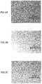
- FIGS.2A, 2B and 2C are images of the surfaces of the respective second nitride semiconductor layers of Samples 1, 4 and 5 observed under an optical microscope. As shown in Table 1, cracks are observed on the surface of the second nitride semiconductor layer of Sample 1 shown in FIG.2A , and pits are observed on the surface of the second nitride semiconductor layer of Sample 4 shown in FIG.2B . On the other hand, none of cracks and pits are observed on the surface of the second nitride semiconductor layer of Sample 5 shown in FIG.2C .
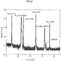
- FIG.3 is an X-ray diffraction pattern of the nitride semiconductor template as Sample 5.
- the X-ray diffraction pattern in FIG.3 only has peaks of diffraction from the Ga 2 O 3 substrate at a (- 201 ) plane and planes parallel to the (- 201 ) plane, from AlN as the first nitride semiconductor layer at a plane parallel to a ( 0001 ) plane and from Al 0.3 Ga 0.7 N as the second nitride semiconductor layer at planes parallel to a ( 0001 ) plane, and shows that the second nitride semiconductor layer does not have a phase grown in a different direction.
- the Al composition is shown as Al 0.29 Ga 0.71 N in FIG.3 since the Al composition of Al 0.3 Ga 0.7 N was actually 0.29 as a result of calculation based on complete lattice relaxation derived from the peak position.
- FIG.4 shows photoluminescence spectra of the nitride semiconductor template as Sample 5. This spectrum was obtained by photoluminescence measurement using excitation light with a wavelength of 244 nm at room temperature, and the peak at a wavelength of 305 nm probably due to band edge emission is shown as a main peak.
- a nitride semiconductor template which has a high-quality nitride semiconductor on a Ga 2 O 3 substrate and is suitable for use in a UV LED with an emission wavelength of 315 to 360 nm.
- a transparent nitride semiconductor template that includes a high-quality nitride semiconductor, is suitable for use in an ultraviolet LED and has electrical conductivity, as well as a manufacturing method that allows simple manufacture of the transparent nitride semiconductor template.
Landscapes
- Chemical & Material Sciences (AREA)
- Engineering & Computer Science (AREA)
- Crystallography & Structural Chemistry (AREA)
- Materials Engineering (AREA)
- Metallurgy (AREA)
- Organic Chemistry (AREA)
- Inorganic Chemistry (AREA)
- Chemical Kinetics & Catalysis (AREA)
- General Chemical & Material Sciences (AREA)
- Led Devices (AREA)
- Crystals, And After-Treatments Of Crystals (AREA)
- Recrystallisation Techniques (AREA)
Abstract
[Problem] To provide a transparent nitride semiconductor template having a high-quality nitride semiconductor, being suitable for use in an ultraviolet LED, and having electroconductivity, and a manufacturing method allowing simple manufacture of same. [Solution] Provided is a nitride semiconductor template 10 having: a Ga 2 O 3 substrate 11; a buffer layer 12 formed on the Ga 2 O 3 substrate 11 and having AlN as a principal component; a first nitride semiconductor layer 13 formed on the buffer layer 12 and having Al x Ga 1-x N (0.2 < x ¤ 1) as a principal component; and a second nitride semiconductor layer 14 formed on the first nitride semiconductor layer 13 and having Al y Ga 1-y N (0.2 ¤ y ¤ 0.55, y < x) as a principal component.
Description
- The invention relates to a nitride semiconductor template and a method for manufacturing the nitride semiconductor template.
- A nitride semiconductor template is known in which a nitride semiconductor layer is formed on a Ga2O3 substrate via an AlN buffer layer (see, e.g., PTL 1)
- According to PTL 1, appropriately selecting a plane orientation of a main surface of the Ga2O3 substrate allows the nitride semiconductor layer to have a mirror surface.
- [PTL 1]
JP-A 2014-199935 - When forming a nitride semiconductor on the Ga2O3 substrate, however, the conditions to prevent pits or cracks on the nitride semiconductor are different depending on the amount of the Al composition of the nitride semiconductor. Therefore, the optimal method needs to be chosen for each composition to obtain a higher-quality nitride semiconductor.
- In recent years, ultraviolet LEDs in the wavelength range of 315 to 360 nm have been developed as an alternative to high-pressure mercury lamps used for curing, etc.
- It is an object of the invention to provide a transparent nitride semiconductor template that includes a high-quality nitride semiconductor, is suitable for use in an ultraviolet LED and has an electrical conductivity, as well as a manufacturing method that allows simple manufacture of the transparent nitride semiconductor template.
- To achieve the above-mentioned object, an aspect of the invention provides a nitride semiconductor template described in the following [1] to [5] and a method for manufacturing a nitride semiconductor template described in the following [6] to [8].
- [1] A nitride semiconductor template, comprising: a Ga2O3 substrate; a buffer layer formed on the Ga2O3 substrate and comprising AlN as a principal component; a first nitride semiconductor layer formed on the buffer layer and comprising AlxGa1-xN (0.2<x≤1) as a principal component; and a second nitride semiconductor layer formed on the first nitride semiconductor layer and comprising AlyGa1-yN (0.2≤y≤0.55, y<x) as a principal component.
- [2] The nitride semiconductor template described in [1], wherein the buffer layer is not more than 10 nm in thickness.
- [3] The nitride semiconductor template described in [1] or [2], wherein the second nitride semiconductor layer has no crack on a surface thereof.
- [4] The nitride semiconductor template described in [1] or [2], wherein the second nitride semiconductor layer has no pit on a surface thereof.
- [5] The nitride semiconductor template described in [1] or [2], wherein the second nitride semiconductor layer has a dislocation density of not more than 2.0x1010 cm-2.
- [6] A method for manufacturing a nitride semiconductor template, comprising: a step of forming a Ga2O3 substrate; a step of forming a buffer layer comprising AlN as a principal component on the Ga2O3 substrate; a step of forming a first nitride semiconductor layer comprising AlxGa1-xN (0.2<x≤1) as a principal component on the buffer layer; and a step of forming a second nitride semiconductor layer comprising AlyGa1-yN (0.2≤y≤0.55, y<x) as a principal component on the first nitride semiconductor layer.
- [7] The method for manufacturing a nitride semiconductor template described in [6], wherein the buffer layer is not more than 10 nm in thickness.
- [8] The method for manufacturing a nitride semiconductor template described in [6] or [7], wherein a growth temperature of the second nitride semiconductor layer is more than 1100°C, and a growth temperature of the first nitride semiconductor layer is less than 1100°C.
- According to the invention, a transparent nitride semiconductor template can be provided that includes a high-quality nitride semiconductor, is suitable for use in an ultraviolet LED and has electrical conductivity, as well as a manufacturing method that allows simple manufacture of the transparent nitride semiconductor template.
-
-
FIG.1 is a vertical cross-sectional view showing a nitride semiconductor template in an embodiment. -
FIG.2A is an image of a surface of a second nitride semiconductor layer of Sample 1 observed under an optical microscope. -
FIG.2B is an image of a surface of a second nitride semiconductor layer of Sample 4 observed under an optical microscope. -
FIG.2C is an image of a surface of a second nitride semiconductor layer of Sample 5 observed under an optical microscope. -
FIG.3 is an X-ray diffraction pattern of the nitride semiconductor template as Sample 5 obtained using a symmetrical reflection method. -
FIG.4 shows photoluminescence spectra of the nitride semiconductor template as Sample 5. -
FIG.1 is a vertical cross-sectional view showing anitride semiconductor template 10 in the embodiment. Thenitride semiconductor template 10 is a template suitable for use in an ultraviolet LED with an emission wavelength of 315 to 360 nm. - The
nitride semiconductor template 10 includes a Ga2O3 substrate 11, abuffer layer 12 on the Ga2O3 substrate 11, a firstnitride semiconductor layer 13 on thebuffer layer 12, and a secondnitride semiconductor layer 14 on the firstnitride semiconductor layer 13. - The Ga2O3 substrate 11 is formed of a β-Ga2O3 single crystal. The main surface of the Ga2O3 substrate 11 is a (-201) plane, a (101) plane, a (310) plane, a (3-10) plane or planes inclined from these planes within a range of about ±2°, which can be a base for growth of high-quality nitride semiconductor crystal. The Ga2O3
substrate 11 is, e.g., a circular substrate having a diameter of 50.8 mm (2 inches), but the shape and size thereof are not limited. - Since Ga2O3 hardly absorbs light with a wavelength of 315 to 360 nm, the Ga2O3 substrate 11 is excellent as a substrate of the
nitride semiconductor template 10 which is used to form an UV LED with an emission wavelength of 315 to 360 nm. By contrast, e.g., GaN absorbs light with a wavelength of 315 to 360 nm well. Therefore, GaN substrates are not suitable as UV LED templates, and to prevent a decrease in light extraction efficiency, the GaN substrates need to be removed after manufacturing LEDs. - In addition, the Ga2O3
substrate 11, which contains a dopant such as Si or Sn and has excellent conductivity, is excellent as an LED substrate. On the other hand, in case that a low-conductivity substrate, e.g., a sapphire substrate, is used, it is not possible to form vertical-type LEDs, and horizontal-type LEDs, even when formed, have high electrical resistance since an electric current flows through a thin nitride semiconductor layer on the substrate. - The
buffer layer 12 is formed of a crystal consisting mainly of AlN. Thebuffer layer 12 may partially cover the upper surface of the Ga2O3 substrate 11 as shown inFIG.1 , or may cover the entire upper surface. To obtain higher crystal quality, the thickness of thebuffer layer 12 is preferably not more than 10 nm, more preferably, not more than 5 nm. - The second
nitride semiconductor layer 14 is used as a cladding layer in a UV LED which is formed using thenitride semiconductor template 10. To form a UV LED with an emission wavelength of 315 to 360 nm, the secondnitride semiconductor layer 14 to be a cladding layer need to have a composition roughly represented by AlyGa1-yN (0.2≤y≤0.55). - The Al composition of the first
nitride semiconductor layer 13 is greater than that of the secondnitride semiconductor layer 14. In other words, the composition of the firstnitride semiconductor layer 13 is expressed by AlxGa1-xN (0.2<x≤1), and the Al composition-x of the firstnitride semiconductor layer 13 and the Al composition-y of the secondnitride semiconductor layer 14 satisfy the relation of y<x. The firstnitride semiconductor layer 13 having such a composition allows the secondnitride semiconductor layer 14 to have a mirror surface and generation of cracks and pits to be suppressed. - The first
nitride semiconductor layer 13 and the secondnitride semiconductor layer 14 may contain a dopant such as Si. The thickness of the firstnitride semiconductor layer 13 is, e.g., 100 to 300 nm. The thickness of the secondnitride semiconductor layer 14 is, e.g., 1 to 2 µm. - The surface of the second
nitride semiconductor layer 14 is a mirror surface and hardly contains, or does not contain cracks and pits (hole-like defects) at all. - If the second
nitride semiconductor layer 14 is formed on thebuffer layer 12 without providing the firstnitride semiconductor layer 13, cracks are generated on the surface of the secondnitride semiconductor layer 14. Meanwhile, when only the firstnitride semiconductor layer 13 is formed on thebuffer layer 12 without providing the secondnitride semiconductor layer 14, a mirror surface cannot be obtained. - An example method for manufacturing the
nitride semiconductor template 10 will be described below. - Firstly, the Ga2O3 substrate 11 treated by CMP (Chemical Mechanical Polishing) is cleaned with an organic solvent and SPM (Sulfuric acid/hydrogen peroxide mixture).
- Next, the Ga2O3 substrate 11 is conveyed to a chamber of a MOCVD (Metal Organic Chemical Vapor Deposition) apparatus.
- Next, the
buffer layer 12 is formed on the Ga2O3 substrate 11. An AlN crystal is grown on the Ga2O3 substrate 11 by supplying source gases and N2 gas as a carrier gas into the chamber in a state that the temperature inside the chamber is maintained at 400 to 600°C, thereby forming thebuffer layer 12 in the form of film. - The source gases used to form the
buffer layer 12 are, e.g., trimethylaluminum (TMA) gas as an Al source and NH3 gas as an N source. The carrier gas may be alternatively H2 gas, etc. - Next, the first
nitride semiconductor layer 13 is formed on thebuffer layer 12. In detail, for example, source gases for the firstnitride semiconductor layer 13 and H2 gas as a carrier gas are supplied into the chamber with pressure maintained at 100 mbar and temperature maintained at not less than 885°C, thereby growing the firstnitride semiconductor layer 13. - The source gases used to form the
nitride semiconductor layer 13 are, e.g., trimethylaluminum (TMA) gas as an Al source, trimethylgallium (TMG) gas as Ga source and NH3 gas as an N source. The carrier gas may be alternatively N2 gas, etc. - Next, the second
nitride semiconductor layer 14 is formed on the firstnitride semiconductor layer 13. In detail, for example, source gases for the secondnitride semiconductor layer 14 and H2 gas as a carrier gas are supplied into the chamber with temperature maintained at not less than 1100°C, thereby growing the secondnitride semiconductor layer 14. - Here, generation of pits can be suppressed when the second
nitride semiconductor layer 14 is grown at a growth temperature of more than 1100°C. Furthermore, generation of pits can be suppressed more reliably when the secondnitride semiconductor layer 14 is grown at a growth temperature of not less than 1120°C. - The source gases for the second
nitride semiconductor layer 14 may be the same as those for the firstnitride semiconductor layer 13. The carrier gas may be alternatively N2 gas, etc. - Table 1 below shows the growth conditions of each layer and the results of evaluating the surface state of the second nitride semiconductor layers.
- Each of the Ga2O3 substrates of seven types of nitride semiconductor templates (Samples 1 to 7) used for evaluation was a 2 inch-diameter circular substrate having a (-201) plane as the main surface. Trimethylaluminum (TMA) gas, trimethylgallium (TMG) gas and NH3 gas were respectively used as the Al source, the Ga source and the N source for the first and second nitride semiconductor layers.
Table 1 Sample No. Buffer layer First nitride semiconductor layer Second nitride semiconductor layer Surface state Film thickness [nm] Growth temperature [°C] Composition Growth temperature [°C] Composition Growth temperature [°C] Check of etched Ga2O3 substrate Pit Crack 1 5 550 N/A N/A Al0.3Ga0.7N 1100 Etched Observed Observed 2 5 800 N/A N/A Al0.3Ga0.7N 1100 Etched Observed Observed 3 5 550 Al0.3Ga0.7N 1020 Al0.3Ga0.7N 1100 Not etched Observed Observed 4 5 550 AlN 1020 Al0.3Ga0.7N 1100 Not etched Observed Not observed 5 5 550 AlN 1020 Al0.3Ga0.7N 1120 Not etched Not observed Not observed 6 5 550 Al0.8Ga0.2N 1020 Al0.3Ga0.7N 1120 Not etched Not observed Not observed 7 5 550 Al0.8Ga0.2N 1020 Al0.45Ga0.55N 1120 Not etched Not observed Not observed - The second nitride semiconductor layer of each of Samples 1 to 7 was grown at a growth rate of 2 µm/h.
- In Samples 1 and 2, the second nitride semiconductor layer was directly formed on the buffer layer without forming the first nitride semiconductor layer. Pits and cracks were generated on the surface of the second nitride semiconductor layer of Sample 1 and a mirror surface was obtained only in a 25 mm-diameter region. Likewise, pits and cracks were generated also on the surface of the second nitride semiconductor layer of Sample 2. It is considered that this is because the first nitride semiconductor layer was not formed.
- Meanwhile, in Sample 1, the Ga2O3 substrate was partially etched. The reason is considered as follows: since the second nitride semiconductor layer to be grown at a higher temperature than the first nitride semiconductor layer was directly formed on the buffer layer, the buffer layer migrated (or crystallized) too much and thus did not sufficiently protect some portion of the surface of the Ga2O3 substrate. On the other hand, in Sample 2, the Ga2O3 substrate was etched when forming the buffer layer since the growth temperature of the buffer layer was too high.
- In Sample 3, cracks were generated on the surface of the second nitride semiconductor layer. It is considered that this is because the Al composition of the first nitride semiconductor layer was the same as that of the second nitride semiconductor layer.
- In Sample 4, pits were generated on the surface of the second nitride semiconductor layer. It is considered that this is because growth of the crystal in the lateral direction was insufficient when the second nitride semiconductor layer was grown at a temperature of 1100°C.
- In Sample 5, none of cracks and pits were generated on the surface of the second nitride semiconductor layer. It is considered that this is mainly because the first and second nitride semiconductor layers were both formed and the Al composition of the second nitride semiconductor layer was smaller than that of the first nitride semiconductor layer. The reason why pits were not generated is considered that the second nitride semiconductor layer was grown at a temperature of 1120°C, i.e., higher than 1100°C.
- Sample 6 was the same as Sample 5, except that the material of the first nitride semiconductor layer was changed to Al0.8Ga0.2N from AlN to decrease electrical resistance of the first nitride semiconductor layer. Also in Sample 6, none of cracks and pits were generated.
- In Sample 7, the Al composition of the second nitride semiconductor layer was increased to more than that of Samples 5 and 6 for use in LEDs with a short wavelength. Also in Sample 7, none of cracks and pits were generated.
- In all of Samples 1 to 7, dislocation density in the second nitride semiconductor layer was suppressed to not more than 2.0x1010 cm-2.
- It is understood from the evaluation results of Samples 1 to 7 that the conditions to obtain the second nitride semiconductor layer with a good surface state are that the first and second nitride semiconductor layers are both formed, that the Al composition of the second nitride semiconductor layer is smaller than that of the first nitride semiconductor layer, and that the growth temperature of the second nitride semiconductor layer is more than 1100°C.
-
FIGS.2A, 2B and 2C are images of the surfaces of the respective second nitride semiconductor layers of Samples 1, 4 and 5 observed under an optical microscope. As shown in Table 1, cracks are observed on the surface of the second nitride semiconductor layer of Sample 1 shown inFIG.2A , and pits are observed on the surface of the second nitride semiconductor layer of Sample 4 shown inFIG.2B . On the other hand, none of cracks and pits are observed on the surface of the second nitride semiconductor layer of Sample 5 shown inFIG.2C . -
FIG.3 is an X-ray diffraction pattern of the nitride semiconductor template as Sample 5. - The X-ray diffraction pattern in
FIG.3 only has peaks of diffraction from the Ga2O3 substrate at a (-201) plane and planes parallel to the (-201) plane, from AlN as the first nitride semiconductor layer at a plane parallel to a (0001) plane and from Al0.3Ga0.7N as the second nitride semiconductor layer at planes parallel to a (0001) plane, and shows that the second nitride semiconductor layer does not have a phase grown in a different direction. Note that, the Al composition is shown as Al0.29Ga0.71N inFIG.3 since the Al composition of Al0.3Ga0.7N was actually 0.29 as a result of calculation based on complete lattice relaxation derived from the peak position. - Meanwhile, as a result of x-ray rocking curve measurement on the nitride semiconductor template as Sample 5, the full width at half maximum of diffraction peak from a (0002) plane was 1164 arcseconds and the full width at half maximum of diffraction peak from a (1-102) plane was 1536 arcseconds.
-
FIG.4 shows photoluminescence spectra of the nitride semiconductor template as Sample 5. This spectrum was obtained by photoluminescence measurement using excitation light with a wavelength of 244 nm at room temperature, and the peak at a wavelength of 305 nm probably due to band edge emission is shown as a main peak. - In the embodiment, it is possible to obtain a nitride semiconductor template which has a high-quality nitride semiconductor on a Ga2O3 substrate and is suitable for use in a UV LED with an emission wavelength of 315 to 360 nm.
- Although the embodiment of the invention has been described, the invention is not intended to be limited to the embodiment, and the various kinds of modifications can be implemented without departing from the gist of the invention.
- In addition, the invention according to claims is not to be limited to embodiment. Further, it should be noted that all combinations of the features described in the embodiment are not necessary to solve the problem of the invention.
- Provided is a transparent nitride semiconductor template that includes a high-quality nitride semiconductor, is suitable for use in an ultraviolet LED and has electrical conductivity, as well as a manufacturing method that allows simple manufacture of the transparent nitride semiconductor template.
-
- 10 NITRIDE SEMICONDUCTOR TEMPLATE
- 11 Ga2O3 SUBSTRATE
- 12 BUFFER LAYER
- 13 FIRST NITRIDE SEMICONDUCTOR LAYER
- 14 SECOND NITRIDE SEMICONDUCTOR LAYER
Claims (8)
- A nitride semiconductor template, comprising:a Ga2O3 substrate;a buffer layer formed on the Ga2O3 substrate and comprising AlN as a principal component;a first nitride semiconductor layer formed on the buffer layer and comprising AlxGa1-xN (0.2<x≤1) as a principal component; anda second nitride semiconductor layer formed on the first nitride semiconductor layer and comprising AlyGa1-yN (0.2≤y≤0.55, y<x) as a principal component.
- The nitride semiconductor template according to claim 1, wherein the buffer layer is not more than 10 nm in thickness.
- The nitride semiconductor template according to claim 1 or 2, wherein the second nitride semiconductor layer has no crack on a surface thereof.
- The nitride semiconductor template according to claim 1 or 2, wherein the second nitride semiconductor layer has no pit on a surface thereof.
- The nitride semiconductor template according to claim 1 or 2, wherein the second nitride semiconductor layer has a dislocation density of not more than 2.0x1010 cm-2.
- A method for manufacturing a nitride semiconductor template, comprising:a step of forming a Ga2O3 substrate;a step of forming a buffer layer comprising AlN as a principal component on the Ga2O3 substrate;a step of forming a first nitride semiconductor layer comprising AlxGa1-xN (0.2<x≤1) as a principal component on the buffer layer; anda step of forming a second nitride semiconductor layer comprising AlyGa1-yN (0.2≤y≤0.55, y<x) as a principal component on the first nitride semiconductor layer.
- The method for manufacturing a nitride semiconductor template according to claim 6, wherein the buffer layer is not more than 10 nm in thickness.
- The method for manufacturing a nitride semiconductor template according to claim 6 or 7, wherein a growth temperature of the second nitride semiconductor layer is more than 1100°C, and a growth temperature of the first nitride semiconductor layer is less than 1100°C.
Applications Claiming Priority (2)
| Application Number | Priority Date | Filing Date | Title |
|---|---|---|---|
| JP2015035895A JP6195125B2 (en) | 2015-02-25 | 2015-02-25 | Nitride semiconductor template and manufacturing method thereof |
| PCT/JP2016/053695 WO2016136446A1 (en) | 2015-02-25 | 2016-02-08 | Nitride semiconductor template and method for manufacturing same |
Publications (1)
| Publication Number | Publication Date |
|---|---|
| EP3264445A1 true EP3264445A1 (en) | 2018-01-03 |
Family
ID=56789281
Family Applications (1)
| Application Number | Title | Priority Date | Filing Date |
|---|---|---|---|
| EP16755193.6A Withdrawn EP3264445A1 (en) | 2015-02-25 | 2016-02-08 | Nitride semiconductor template and method for manufacturing same |
Country Status (6)
| Country | Link |
|---|---|
| US (1) | US20180033907A1 (en) |
| EP (1) | EP3264445A1 (en) |
| JP (1) | JP6195125B2 (en) |
| CN (1) | CN107251195A (en) |
| TW (1) | TW201705530A (en) |
| WO (1) | WO2016136446A1 (en) |
Families Citing this family (2)
| Publication number | Priority date | Publication date | Assignee | Title |
|---|---|---|---|---|
| WO2019156121A1 (en) * | 2018-02-08 | 2019-08-15 | 住友化学株式会社 | Semiconductor wafer |
| CN109301044A (en) * | 2018-10-15 | 2019-02-01 | 华中科技大学鄂州工业技术研究院 | Deep ultraviolet LED vertical chip based on n-type doped gallium oxide front-mounted structure |
Family Cites Families (10)
| Publication number | Priority date | Publication date | Assignee | Title |
|---|---|---|---|---|
| US7687827B2 (en) * | 2004-07-07 | 2010-03-30 | Nitronex Corporation | III-nitride materials including low dislocation densities and methods associated with the same |
| JP5491065B2 (en) * | 2009-04-30 | 2014-05-14 | 住友電気工業株式会社 | Method for producing wafer product and method for producing gallium nitride based semiconductor optical device |
| KR101317735B1 (en) * | 2009-09-07 | 2013-10-15 | 도꾸리쯔교세이호징 리가가쿠 겐큐소 | Nitride semiconductor multilayer structure and method for manufacturing the same, and nitride semiconductor light emitting device |
| US9153648B2 (en) * | 2011-04-08 | 2015-10-06 | Tamura Corporation | Semiconductor stacked body, method for manufacturing same, and semiconductor element |
| US9716004B2 (en) * | 2011-09-08 | 2017-07-25 | Tamura Corporation | Crystal laminate structure and method for producing same |
| KR20140085508A (en) * | 2011-10-13 | 2014-07-07 | 가부시키가이샤 다무라 세이사쿠쇼 | Crystal layered structure and method for manufacturing same, and semiconductor element |
| CN103247724B (en) * | 2012-02-08 | 2016-04-20 | 郭磊 | A kind of semiconductor structure and forming method thereof |
| JP2013214686A (en) * | 2012-04-04 | 2013-10-17 | Furukawa Co Ltd | Group iii nitride semiconductor layer and group iii nitride semiconductor layer manufacturing method |
| JP2013251439A (en) * | 2012-06-01 | 2013-12-12 | Tamura Seisakusho Co Ltd | Semiconductor stacked structure and semiconductor element |
| JP2015005534A (en) * | 2013-06-18 | 2015-01-08 | 学校法人立命館 | Vertical type light-emitting diode, and crystal growth method |
-
2015
- 2015-02-25 JP JP2015035895A patent/JP6195125B2/en active Active
-
2016
- 2016-02-08 US US15/551,960 patent/US20180033907A1/en not_active Abandoned
- 2016-02-08 WO PCT/JP2016/053695 patent/WO2016136446A1/en not_active Ceased
- 2016-02-08 CN CN201680012004.9A patent/CN107251195A/en active Pending
- 2016-02-08 EP EP16755193.6A patent/EP3264445A1/en not_active Withdrawn
- 2016-02-25 TW TW105105673A patent/TW201705530A/en unknown
Also Published As
| Publication number | Publication date |
|---|---|
| CN107251195A (en) | 2017-10-13 |
| JP2016157876A (en) | 2016-09-01 |
| WO2016136446A1 (en) | 2016-09-01 |
| US20180033907A1 (en) | 2018-02-01 |
| JP6195125B2 (en) | 2017-09-13 |
| TW201705530A (en) | 2017-02-01 |
Similar Documents
| Publication | Publication Date | Title |
|---|---|---|
| CN1218374C (en) | Semiconductor substrate based on group III nitride and its manufacturing method thereof | |
| CN101308896B (en) | GaN substrate, epitaxial substrate and semiconductor light emitting device using the substrate | |
| JP6042545B2 (en) | Highly transparent aluminum nitride single crystal layer and device comprising the same | |
| US9209018B2 (en) | Semiconductor substrate and method of manufacturing | |
| US20150200256A1 (en) | Group iii nitride articles having nucleation layers, transitional layers, and bulk layers | |
| US10026869B2 (en) | Nitride semiconductor light-emitting device and method for producing the same | |
| EP2500451A1 (en) | Method for producing laminate | |
| WO2009090821A1 (en) | Process for producing laminate comprising al-based group iii nitride single crystal layer, laminate produced by the process, process for producing al-based group iii nitride single crystal substrate using the laminate, and aluminum nitride single crystal substrate | |
| US8026523B2 (en) | Nitride semiconductor free-standing substrate and device using the same | |
| EP2484816A1 (en) | Method for production of laminate | |
| CN108155279A (en) | Manufacturing method, nitride semiconductor template and the nitride compound semiconductor device of nitride semiconductor template | |
| KR20070058465A (en) | Baa-containing nitride semiconductor single crystal, its production method, and substrate and device using the crystal | |
| US9196480B2 (en) | Method for treating group III nitride substrate and method for manufacturing epitaxial substrate | |
| WO2016136548A1 (en) | Nitride semiconductor template, manufacturing method thereof, and epitaxial wafer | |
| US9520527B1 (en) | Nitride semiconductor template and ultraviolet LED | |
| US20180033907A1 (en) | Nitride semiconductor template and method for manufacturing same | |
| WO2009119159A1 (en) | Substrate for optical device and method for manufacturing the substrate | |
| JP6080148B2 (en) | Aluminum nitride single crystal and method for producing the same | |
| EP3435407B1 (en) | Method for producing group iii nitride laminate | |
| JP2006173148A (en) | Group III nitride semiconductor free-standing substrate and manufacturing method thereof | |
| EP2980862B1 (en) | Manufacturing method for semiconductor light-emitting element, and semiconductor light-emitting element | |
| KR101697462B1 (en) | VERTICAL TYPE ULTRA-VIOLET LIGHT EMITTING DEVICE, METHOD FOR MANUFACTURING OF THE SAME, AlN TEMPLETE FOR VERTICAL TYPE ULTRA-VIOLET LIGHT EMITTING DEVICE AND METHOD FOR MANUFACTURING OF THE SAME | |
| WO2015043961A1 (en) | A semiconductor wafer and a method for producing the semiconductor wafer | |
| US20070034144A1 (en) | Oxide crystal growth apparatus and fabrication method using the same | |
| KR101919360B1 (en) | Light emitting device using the nitride-based semiconductor nano rod and manufacturing method of the same |
Legal Events
| Date | Code | Title | Description |
|---|---|---|---|
| PUAI | Public reference made under article 153(3) epc to a published international application that has entered the european phase |
Free format text: ORIGINAL CODE: 0009012 |
|
| 17P | Request for examination filed |
Effective date: 20170818 |
|
| AK | Designated contracting states |
Kind code of ref document: A1 Designated state(s): AL AT BE BG CH CY CZ DE DK EE ES FI FR GB GR HR HU IE IS IT LI LT LU LV MC MK MT NL NO PL PT RO RS SE SI SK SM TR |
|
| AX | Request for extension of the european patent |
Extension state: BA ME |
|
| DAV | Request for validation of the european patent (deleted) | ||
| DAX | Request for extension of the european patent (deleted) | ||
| STAA | Information on the status of an ep patent application or granted ep patent |
Free format text: STATUS: THE APPLICATION HAS BEEN WITHDRAWN |
|
| 18W | Application withdrawn |
Effective date: 20180614 |