EP3264253A1 - Riser-karte - Google Patents
Riser-karte Download PDFInfo
- Publication number
- EP3264253A1 EP3264253A1 EP17178359.0A EP17178359A EP3264253A1 EP 3264253 A1 EP3264253 A1 EP 3264253A1 EP 17178359 A EP17178359 A EP 17178359A EP 3264253 A1 EP3264253 A1 EP 3264253A1
- Authority
- EP
- European Patent Office
- Prior art keywords
- interface
- data ports
- switching module
- routing
- routing mode
- Prior art date
- Legal status (The legal status is an assumption and is not a legal conclusion. Google has not performed a legal analysis and makes no representation as to the accuracy of the status listed.)
- Withdrawn
Links
Images



Classifications
-
- G—PHYSICS
- G06—COMPUTING OR CALCULATING; COUNTING
- G06F—ELECTRIC DIGITAL DATA PROCESSING
- G06F13/00—Interconnection of, or transfer of information or other signals between, memories, input/output devices or central processing units
- G06F13/38—Information transfer, e.g. on bus
- G06F13/40—Bus structure
- G06F13/4004—Coupling between buses
- G06F13/4022—Coupling between buses using switching circuits, e.g. switching matrix, connection or expansion network
-
- G—PHYSICS
- G06—COMPUTING OR CALCULATING; COUNTING
- G06F—ELECTRIC DIGITAL DATA PROCESSING
- G06F13/00—Interconnection of, or transfer of information or other signals between, memories, input/output devices or central processing units
- G06F13/14—Handling requests for interconnection or transfer
- G06F13/16—Handling requests for interconnection or transfer for access to memory bus
-
- G—PHYSICS
- G06—COMPUTING OR CALCULATING; COUNTING
- G06F—ELECTRIC DIGITAL DATA PROCESSING
- G06F13/00—Interconnection of, or transfer of information or other signals between, memories, input/output devices or central processing units
- G06F13/38—Information transfer, e.g. on bus
- G06F13/40—Bus structure
- G06F13/4063—Device-to-bus coupling
- G06F13/4068—Electrical coupling
-
- G—PHYSICS
- G06—COMPUTING OR CALCULATING; COUNTING
- G06F—ELECTRIC DIGITAL DATA PROCESSING
- G06F13/00—Interconnection of, or transfer of information or other signals between, memories, input/output devices or central processing units
- G06F13/38—Information transfer, e.g. on bus
- G06F13/40—Bus structure
- G06F13/4063—Device-to-bus coupling
- G06F13/409—Mechanical coupling
- G06F13/4095—Mechanical coupling in incremental bus architectures, e.g. bus stacks
-
- G—PHYSICS
- G06—COMPUTING OR CALCULATING; COUNTING
- G06F—ELECTRIC DIGITAL DATA PROCESSING
- G06F3/00—Input arrangements for transferring data to be processed into a form capable of being handled by the computer; Output arrangements for transferring data from processing unit to output unit, e.g. interface arrangements
- G06F3/06—Digital input from, or digital output to, record carriers, e.g. RAID, emulated record carriers or networked record carriers
- G06F3/0601—Interfaces specially adapted for storage systems
- G06F3/0668—Interfaces specially adapted for storage systems adopting a particular infrastructure
- G06F3/0671—In-line storage system
- G06F3/0683—Plurality of storage devices
- G06F3/0688—Non-volatile semiconductor memory arrays
Definitions
- the subject matter herein generally relates to a riser card. More specifically, the subject matter herein relates to a riser card configured to convert one or more M.2 (previously known as Next Generation Form Factor (NGFF)) components to work with a U.2 connector (previously known as SFF-8639).
- M.2 previously known as Next Generation Form Factor (NGFF)
- NGFF Next Generation Form Factor
- U.2 components such as Non-Volatile Memory Express (NVMe) peripheral component interconnect express (PCIe) solid state drives (SSD), offer high performance, but are relatively new to market and thus have significant cost.
- NVMe Non-Volatile Memory Express
- PCIe peripheral component interconnect express
- SSD solid state drives
- M.2 (previously known as Next Generation Form Factor (NGFF)) components provide the functionality of a U.2 component with a much smaller form factor and at a significantly reduced cost.
- M.2 can support PCIe with lower power consumption, cost, and maintain a high performance.
- NGFF Next Generation Form Factor
- Coupled is defined as connected, whether directly or indirectly through intervening components, and is not necessarily limited to physical connections.
- the connection can be such that the objects are permanently connected or releasably connected.
- substantially is defined to be essentially conforming to the particular dimension, shape or other word that substantially modifies, such that the component need not be exact.
- substantially cylindrical means that the object resembles a cylinder, but can have one or more deviations from a true cylinder.
- comprising means "including, but not necessarily limited to”; it specifically indicates open-ended inclusion or membership in a so-described combination, group, series and the like.
- the present disclosure describes an apparatus having a first interface of a first type supporting a plurality of data ports, a second interface of a second type supporting at least a portion of the plurality data ports, and a third interface of the second type.
- a switching module coupled to a control port of the first interface and configured for selectably coupling the plurality of data ports to at least one of the second interface and the third interface based on a signal at the control port.
- the switching module selectably connecting the plurality of data ports to one of the second interfaces or diving the plurality of data ports between the two second interfaces.
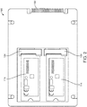
- FIGS. 1-3 illustrate a riser card 100 have a first interface 102, two second interfaces 104, and a switching module 106.
- the first interface 102 can have a plurality of data ports 108 capable of transmitting data between the first interface 102 and the second interface 104.
- the first interface 102 can have a control port 110 configured to selectably couple the plurality of data ports 108 to at least one of the second interfaces 104 based on a signal at the control port 110.
- the first interface 102 and the second interfaces 104 can be of two different types, the first interface having a first type and the second interfaces having a second type.
- the first interface 102 type is an NVMe SSD interface configured to be received in a U.2 connector and the second interface 104 type 104 are M.2 interfaces.
- the riser card 100 can have two receiving portions 112 corresponding to each of the two second interfaces 104.
- the receiving portions 112 can be configured to receive a component 114 (shown in FIG. 3 ), such as an M.2 PCIe SSD at least including three length types of M.2. PCIe SSD 2242, 2260, and 2280 as specified in the M.2 standard.
- the riser card 102 can be configured to selectively receive a component 114 in either of the two receiving portions 112, or both.
- the first interface 102 can be receivable into a U.2 connector 200 disposed on an electronic device (not shown).
- the first interface 102 can electronically couple with the U.2 connector 200 allowing the two second interfaces 104 to send and receive data with the electronic device through the first interface 102.
- the plurality of data ports 108 can be any number of data ports, such as two, four, six, or any other number.
- the riser card 100 has four data ports coupling the first interface 102 with the second interfaces 104.
- the switching module 106 can allocate the plurality of data ports 108 between the first interface 102 and the two second interface 104. A user can control the switching module 106 to best allocate the plurality of data ports 108 according to their desired use, the installed components, and the performance required.
- the riser card 100 can have a one component 114 received in a second interface 104 allowing allocation of the plurality of data ports 108 to the component 114.
- the riser card 100 can receive two components 114 requiring the switching module 106 to allocate the plurality of data ports 108 among the two components 114 received in the second interfaces 104.
- the riser card 100 can receive two components, and a user can allocate the plurality of ports 108 between the two received components 114 allowing utilization of one, or a combination of received components 114.
- the riser card 100 can support hot-swapping of components 114 received in the second interfaces 104. Hot-swapping allows components to be removed, inserted, or replaced from the second interface 104 without removing power from the riser card 100.
- the riser card 100 is received within an electronic device and hot-swapping allows one or more components 114 to be inserted or removed from the riser card 100 without powering down the electronic device.
- Hot-swapping can be implemented using existing pin arrangements with the first interface 102.
- the first interface 102 is a U.2 connector, thereby implementing P12V, P3V3_STBY, and applying the metal-oxide-semiconductor field-effect transistor (MOSFET) to achieve isolation of power hot-swapping is achievable.
- MOSFET metal-oxide-semiconductor field-effect transistor
- the riser card 100 can also implement Electrically Erasable Programmable Read-Only Memory (EEPROM) and hardware monitoring allowing temperature detection, voltage readings while following M.2 standard specifications.
- EEPROM Electrically Erasable Programmable Read-Only Memory
- the EEPROM can include the FRU allowing a technician to maintain and repair the system.
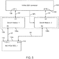
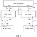
- FIGS. 4-6 illustrate a system diagram of the riser card 100 and the plurality of data ports 108.
- the system diagram shows mapping for the plurality of data ports coupling the first interface 102 with the two second interfaces 104.
- the first interface 102 and second interfaces 104 are coupled by the switching module 106.
- the switching module 106 allows users to select the measurement system of the riser card 100.
- the riser card 100 can support PCIe 1x4 and 2x2 and allow a user to select the measurement system in order to control the switch module.
- the switching module 106 can be a multiplexer (MUX) having a plurality Intergrated Circuits (IC) with multiplexing capability and a routing design configured to avoid propagation delay and allow successful transition of PCIe 1x4 and PCIe 2x2.
- the switching module 106 can be a chip, a field-programmable gate array (FPGA), or any other controller.
- the switching module 106 can be any PCIe switch supporting a PCIe high speed signal.
- the switching module 106 can allow the riser card 100 to operate a component 114 in a PCIe 1x4 arrangement allowing all of the plurality of data ports 108 to be utilized by one component 114.
- the switching module 106 can also support PCIe 2x2, allowing a portion of the plurality of data ports 108 to one of the second interfaces 104 and the remaining portion of the plurality of data ports 108 to the other second interface 104.
- PCIe 2x2 can allow the system to achieve maximum benefits on dual path redundancy, increased performance, and increasing the elasticity of the system structure while lowering the cost of design and overall complexity.
- the switching module 106 is coupled to a control port 118 of the first interface 102 and configured for selectably coupling the plurality of data ports to at least one of the second interfaces 104 based on a control signal.
- the control signal When the control signal is low, the system is in PCIe 2x2 and when the control signal is high, the system is in PCIe 1x4.
- the control port 118 is coupled with switch module_2; however, in other embodiments the control port 118 can be coupled with switch module_1, switch module_2, or a combination thereof.
- the switching module 106 can couple a first interface 102 with two second interfaces 104.
- the first interface 102 is shown as an NVMe SSD connector and the second interfaces 104 are shown as M.2 connectors, each receiving an M.2 PCIe SSD component.
- the switch module 106 has two switch modules switch module_1 106a and switch module_2 106b to support PCIe 1x4 and 2x2.
- the first interface 102 has a plurality of data ports 108, shown in FIG. 4 as [0,1] and [0,1]/[2,3], couplable with the second interfaces 104 via the switch module.
- Each second interface 104 can have a corresponding plurality of data ports 116, shown in FIG. 4 as [0,1] and [2,3].
- the switch module 106 is in a second routing mode and receives a control signal corresponding to operating the system in PCIe 1x4.
- the switch module_1 106a connects B1 and A1 while switching module_2 106b connects B2 and A2.
- Switch module_2 shifts to connect first interface 104 connector [2:3] with component 114 [2:3] allowing PCIe 1x4 for system testing.
- FIG. 6 is drawn to B2 of switch module_2 106b connecting with [2,3] of component 114a, other arrangements can be implemented such as C1 of switch module_1 connecting with [2,3] of component 114b, or a combination thereof.
- the switch module 106 is in a first routing mode and receives a control signal corresponding to operating the system in PCIe 2x2.
- C1 (not shown) of switch module_1 106a is not routing while A1 connects to B1 and A2 of switch module_2 106b connects C2.
- Switch module_1 106a connects B1 with component 114a, shown as M.2 PCIe SSD_1 [0:1]
- switch module_2 106b connects C2 with component 114b, shown as M.2 PCI SSD_2 [0:1].
- Each component 114a, 114b receives a portion of the plurality of data ports 108.
- the plurality of data ports 108 is four [0,1] and [2,3] and the portion of the plurality of data ports is two, [0:1].
- Each component 114 is receiving two of the available four data ports. While the illustrated embodiment is drawn to switch module_1 coupling with data ports [0,1] of the first interface 102 and switch module_2 coupling with data ports [2,3], the riser card 100 can be implemented with switch module_1 and switch module_2 reversed.
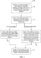
- the example method 700 is provided by way of example, as there are a variety of ways to carry out the method 700.
- the method 700 described below can be carried out using the configurations illustrated in FIGS. 1-6 , for example, and various elements of these figures are referenced in explaining example method 700.
- Each block shown in FIG. 7 represents one or more processes, methods or subroutines, carried out in the example method 700.
- the illustrated order of blocks is illustrative only and the order of the blocks can change according to the present disclosure. Additional blocks may be added or fewer blocks may be utilized, without departing from this disclosure.
- the example method 700 can begin at block 702.
- an apparatus having a first interface of a first type supporting a plurality of a data ports, and a second interface and a third interface of a second type supporting at least a portion of the plurality of data portions, and a switching module, receives, at the switching module, a control signal for selectably coupling the plurality of data portions of the first interface with at least one of the second interface and the third interface.
- the switching module selects, in response to the control signal, a first routing mode or a second routing mode.
- the switching module routes the signals for the plurality of data ports at a first interface to one of the second interface and the third interface.
- the switching module routes at least a portion of the signals for the plurality of data ports to the second interface and the remaining portion of the data ports to the third interface.
- the switching module can monitor apparatus operating temperature, voltage, and operating statistics.
Landscapes
- Engineering & Computer Science (AREA)
- Theoretical Computer Science (AREA)
- General Engineering & Computer Science (AREA)
- Physics & Mathematics (AREA)
- General Physics & Mathematics (AREA)
- Computer Hardware Design (AREA)
- Mathematical Physics (AREA)
- Human Computer Interaction (AREA)
- Information Transfer Systems (AREA)
- Mobile Radio Communication Systems (AREA)
Applications Claiming Priority (1)
| Application Number | Priority Date | Filing Date | Title |
|---|---|---|---|
| US15/199,504 US10289588B2 (en) | 2016-06-30 | 2016-06-30 | Riser card |
Publications (1)
| Publication Number | Publication Date |
|---|---|
| EP3264253A1 true EP3264253A1 (de) | 2018-01-03 |
Family
ID=59276524
Family Applications (1)
| Application Number | Title | Priority Date | Filing Date |
|---|---|---|---|
| EP17178359.0A Withdrawn EP3264253A1 (de) | 2016-06-30 | 2017-06-28 | Riser-karte |
Country Status (5)
| Country | Link |
|---|---|
| US (1) | US10289588B2 (de) |
| EP (1) | EP3264253A1 (de) |
| JP (1) | JP6429211B2 (de) |
| CN (1) | CN107562667B (de) |
| TW (1) | TWI594108B (de) |
Families Citing this family (26)
| Publication number | Priority date | Publication date | Assignee | Title |
|---|---|---|---|---|
| US20160259754A1 (en) | 2015-03-02 | 2016-09-08 | Samsung Electronics Co., Ltd. | Hard disk drive form factor solid state drive multi-card adapter |
| US12561270B2 (en) | 2016-07-26 | 2026-02-24 | Samsung Electronics Co., Ltd. | Self-configuring SSD multi-protocol support in host-less environment |
| US11983138B2 (en) | 2015-07-26 | 2024-05-14 | Samsung Electronics Co., Ltd. | Self-configuring SSD multi-protocol support in host-less environment |
| US10372659B2 (en) * | 2016-07-26 | 2019-08-06 | Samsung Electronics Co., Ltd. | Multi-mode NMVE over fabrics devices |
| US10387353B2 (en) * | 2016-07-26 | 2019-08-20 | Samsung Electronics Co., Ltd. | System architecture for supporting active pass-through board for multi-mode NMVE over fabrics devices |
| US10762023B2 (en) * | 2016-07-26 | 2020-09-01 | Samsung Electronics Co., Ltd. | System architecture for supporting active pass-through board for multi-mode NMVe over fabrics devices |
| US12556417B2 (en) | 2016-07-26 | 2026-02-17 | Samsung Electronics Co., Ltd. | Modular system (switch boards and mid-plane) for supporting 50G or 100G ethernet speeds of FPGA+SSD |
| US11461258B2 (en) | 2016-09-14 | 2022-10-04 | Samsung Electronics Co., Ltd. | Self-configuring baseboard management controller (BMC) |
| US10210123B2 (en) | 2016-07-26 | 2019-02-19 | Samsung Electronics Co., Ltd. | System and method for supporting multi-path and/or multi-mode NMVe over fabrics devices |
| US11144496B2 (en) | 2016-07-26 | 2021-10-12 | Samsung Electronics Co., Ltd. | Self-configuring SSD multi-protocol support in host-less environment |
| US12541480B2 (en) | 2016-07-26 | 2026-02-03 | Samsung Electronics Co., Ltd. | Self-configuring SSD multi-protocol support in host-less environment |
| US10346041B2 (en) | 2016-09-14 | 2019-07-09 | Samsung Electronics Co., Ltd. | Method for using BMC as proxy NVMeoF discovery controller to provide NVM subsystems to host |
| CN108459673A (zh) * | 2017-02-17 | 2018-08-28 | 上海宝存信息科技有限公司 | 转接卡 |
| US11263508B2 (en) * | 2017-09-22 | 2022-03-01 | Samsung Electronics Co., Ltd. | Modular NGSFF module to meet different density and length requirements |
| US10520994B2 (en) * | 2018-01-31 | 2019-12-31 | Facebook, Inc. | Storage cartridge |
| US10649940B2 (en) * | 2018-03-05 | 2020-05-12 | Samsung Electronics Co., Ltd. | Modular system architecture for supporting multiple solid-state drives |
| US11157356B2 (en) | 2018-03-05 | 2021-10-26 | Samsung Electronics Co., Ltd. | System and method for supporting data protection across FPGA SSDs |
| US10409760B1 (en) | 2018-03-09 | 2019-09-10 | Samsung Electronics Co., Ltd. | Adaptive interface high availability storage device |
| WO2019236057A1 (en) * | 2018-06-05 | 2019-12-12 | Hewlett-Packard Development Company, L.P. | Route demultiplexed signal pairs |
| CN108984447B (zh) * | 2018-07-27 | 2022-05-31 | 联想(北京)有限公司 | 一种电子设备的控制方法及电子设备 |
| JP2020144518A (ja) | 2019-03-05 | 2020-09-10 | キオクシア株式会社 | 記憶システム、記憶装置および記憶方法 |
| CN113886309B (zh) * | 2021-10-13 | 2024-07-09 | 北京世宁达科技有限公司 | 具有热插拔结构的pcie模组及机箱 |
| CN116028409B (zh) * | 2023-03-30 | 2023-06-13 | 苏州浪潮智能科技有限公司 | 转接卡、主板、计算机、数据传输方法、设备和介质 |
| TWI851329B (zh) * | 2023-07-07 | 2024-08-01 | 群聯電子股份有限公司 | 裝置控制方法、記憶體儲存裝置及記憶體控制電路單元 |
| CN116737636B (zh) * | 2023-08-11 | 2024-09-10 | 珠海星云智联科技有限公司 | Pcie设备热拔插控制方法及相关装置 |
| US20250133672A1 (en) * | 2023-10-23 | 2025-04-24 | ITI Engineering, LLC | Data transfer cartridge |
Citations (2)
| Publication number | Priority date | Publication date | Assignee | Title |
|---|---|---|---|---|
| US20110219158A1 (en) * | 2010-03-04 | 2011-09-08 | Xyratex Technology Limited | Storage assembly, a physical expander and a method |
| GB2523839A (en) * | 2014-03-07 | 2015-09-09 | Xyratex Tech Ltd | A solid state storage carrier and a storage system |
Family Cites Families (15)
| Publication number | Priority date | Publication date | Assignee | Title |
|---|---|---|---|---|
| US20090063895A1 (en) | 2007-09-04 | 2009-03-05 | Kurt Smith | Scaleable and maintainable solid state drive |
| JP5583052B2 (ja) | 2011-02-25 | 2014-09-03 | 株式会社日立製作所 | 故障予測・対策方法及びクライアントサーバシステム |
| US9553776B2 (en) * | 2011-05-16 | 2017-01-24 | Avocent Huntsville, Llc | System and method for accessing operating system and hypervisors via a service processor of a server |
| TWM449368U (zh) | 2012-10-26 | 2013-03-21 | Bellwether Electronic Corp | 卡緣連接器結構 |
| JP5991485B2 (ja) | 2012-12-18 | 2016-09-14 | 富士ゼロックス株式会社 | 電子機器 |
| US9563260B2 (en) | 2013-03-15 | 2017-02-07 | Intel Corporation | Systems, apparatuses, and methods for synchronizing port entry into a low power state |
| CN104111904B (zh) * | 2013-04-17 | 2017-03-01 | 瑞昱半导体股份有限公司 | 通信装置与设置数据传输的方法 |
| TWM469663U (zh) * | 2013-06-28 | 2014-01-01 | Tuton Technology Co Ltd | 具有ngff模組的堆疊型連接裝置 |
| CN203423276U (zh) | 2013-07-17 | 2014-02-05 | 连展科技电子(昆山)有限公司 | 电连接器 |
| TWM474270U (zh) | 2013-10-16 | 2014-03-11 | Portwell Inc | 一種結合fm.2擴充插槽與fm.2擴充插卡的系統 |
| CN203690574U (zh) | 2014-01-22 | 2014-07-02 | 贝尔威勒电子股份有限公司 | Ngff连接器组件及其结构 |
| WO2016003408A1 (en) * | 2014-06-30 | 2016-01-07 | Hewlett-Packard Development Company, L.P. | Runtime drive detection and configuration |
| US11157200B2 (en) | 2014-10-29 | 2021-10-26 | Hewlett-Packard Development Company, L.P. | Communicating over portions of a communication medium |
| TWI536178B (zh) | 2014-12-04 | 2016-06-01 | 英業達股份有限公司 | 伺服器 |
| US9952634B2 (en) * | 2016-03-28 | 2018-04-24 | Lenovo (Singapore) Pte. Ltd. | Interfacing with multiple components connected to a printed circuit board |
-
2016
- 2016-06-30 US US15/199,504 patent/US10289588B2/en active Active
- 2016-09-07 TW TW105128870A patent/TWI594108B/zh active
- 2016-09-27 CN CN201610852353.3A patent/CN107562667B/zh active Active
-
2017
- 2017-06-23 JP JP2017123135A patent/JP6429211B2/ja active Active
- 2017-06-28 EP EP17178359.0A patent/EP3264253A1/de not_active Withdrawn
Patent Citations (2)
| Publication number | Priority date | Publication date | Assignee | Title |
|---|---|---|---|---|
| US20110219158A1 (en) * | 2010-03-04 | 2011-09-08 | Xyratex Technology Limited | Storage assembly, a physical expander and a method |
| GB2523839A (en) * | 2014-03-07 | 2015-09-09 | Xyratex Tech Ltd | A solid state storage carrier and a storage system |
Also Published As
| Publication number | Publication date |
|---|---|
| TWI594108B (zh) | 2017-08-01 |
| TW201809959A (zh) | 2018-03-16 |
| CN107562667A (zh) | 2018-01-09 |
| US10289588B2 (en) | 2019-05-14 |
| CN107562667B (zh) | 2019-10-11 |
| JP2018005907A (ja) | 2018-01-11 |
| US20180004695A1 (en) | 2018-01-04 |
| JP6429211B2 (ja) | 2018-11-28 |
Similar Documents
| Publication | Publication Date | Title |
|---|---|---|
| US10289588B2 (en) | Riser card | |
| US11041907B2 (en) | Method and system for acquisition of test data | |
| US8645746B2 (en) | Cable redundancy and failover for multi-lane PCI express IO interconnections | |
| US8677176B2 (en) | Cable redundancy and failover for multi-lane PCI express IO interconnections | |
| US11016924B2 (en) | System and method for supporting multi-mode and/or multi-speed non-volatile memory (NVM) express (NVMe) over fabrics (NVMe-oF) devices | |
| US10467111B2 (en) | Implementing cable failover in multiple cable PCI express IO interconnections | |
| US9697156B2 (en) | Detecting and configuring of external IO enclosure | |
| EP2817719A1 (de) | Multiplexer für signale nach verschiedenen protokollen | |
| US8832347B2 (en) | Automatic detection device, system and method for inter-integrated circuit and serial general purpose input/output | |
| US8996775B2 (en) | Backplane controller for managing serial interface configuration based on detected activity | |
| US20190280411A1 (en) | Multi-mode and/or multi-speed non-volatile memory (nvm) express (nvme) over fabrics (nvme-of) device | |
| TW201640369A (zh) | 通道資源的重定向 | |
| CN220773578U (zh) | 通用串行总线接口的测试装置 | |
| CN108153624B (zh) | 适用于ngff插槽的测试电路板 | |
| CN107391321A (zh) | 电子计算机单板及服务器调试系统 | |
| CN106909198B (zh) | 一种外接装置、电子装置及电子系统 | |
| CN109994147B (zh) | 一种固态硬盘的测试装置及方法 | |
| CN111897755A (zh) | 日志抓取方法、装置和转接模块 | |
| CN109766287A (zh) | Usb控制器的控制方法和装置 | |
| CN109766288A (zh) | Usb控制器的控制方法和装置 |
Legal Events
| Date | Code | Title | Description |
|---|---|---|---|
| PUAI | Public reference made under article 153(3) epc to a published international application that has entered the european phase |
Free format text: ORIGINAL CODE: 0009012 |
|
| STAA | Information on the status of an ep patent application or granted ep patent |
Free format text: STATUS: THE APPLICATION HAS BEEN PUBLISHED |
|
| AK | Designated contracting states |
Kind code of ref document: A1 Designated state(s): AL AT BE BG CH CY CZ DE DK EE ES FI FR GB GR HR HU IE IS IT LI LT LU LV MC MK MT NL NO PL PT RO RS SE SI SK SM TR |
|
| AX | Request for extension of the european patent |
Extension state: BA ME |
|
| STAA | Information on the status of an ep patent application or granted ep patent |
Free format text: STATUS: REQUEST FOR EXAMINATION WAS MADE |
|
| 17P | Request for examination filed |
Effective date: 20180629 |
|
| RBV | Designated contracting states (corrected) |
Designated state(s): AL AT BE BG CH CY CZ DE DK EE ES FI FR GB GR HR HU IE IS IT LI LT LU LV MC MK MT NL NO PL PT RO RS SE SI SK SM TR |
|
| STAA | Information on the status of an ep patent application or granted ep patent |
Free format text: STATUS: EXAMINATION IS IN PROGRESS |
|
| 17Q | First examination report despatched |
Effective date: 20190903 |
|
| STAA | Information on the status of an ep patent application or granted ep patent |
Free format text: STATUS: THE APPLICATION HAS BEEN WITHDRAWN |
|
| 18W | Application withdrawn |
Effective date: 20191210 |